US20230400764A1 - Organometallic compound comprising a metal combined with at least one ligand containing four or more fluorine atoms, resist composition comprising the same, and method of fabricating semiconductor device using the same - Google Patents
Organometallic compound comprising a metal combined with at least one ligand containing four or more fluorine atoms, resist composition comprising the same, and method of fabricating semiconductor device using the same Download PDFInfo
- Publication number
- US20230400764A1 US20230400764A1 US18/120,248 US202318120248A US2023400764A1 US 20230400764 A1 US20230400764 A1 US 20230400764A1 US 202318120248 A US202318120248 A US 202318120248A US 2023400764 A1 US2023400764 A1 US 2023400764A1
- Authority
- US
- United States
- Prior art keywords
- integer
- resist composition
- organometallic compound
- resist
- toc
- Prior art date
- Legal status (The legal status is an assumption and is not a legal conclusion. Google has not performed a legal analysis and makes no representation as to the accuracy of the status listed.)
- Granted
Links
Images




Classifications
-
- G—PHYSICS
- G03—PHOTOGRAPHY; CINEMATOGRAPHY; ANALOGOUS TECHNIQUES USING WAVES OTHER THAN OPTICAL WAVES; ELECTROGRAPHY; HOLOGRAPHY
- G03F—PHOTOMECHANICAL PRODUCTION OF TEXTURED OR PATTERNED SURFACES, e.g. FOR PRINTING, FOR PROCESSING OF SEMICONDUCTOR DEVICES; MATERIALS THEREFOR; ORIGINALS THEREFOR; APPARATUS SPECIALLY ADAPTED THEREFOR
- G03F7/00—Photomechanical, e.g. photolithographic, production of textured or patterned surfaces, e.g. printing surfaces; Materials therefor, e.g. comprising photoresists; Apparatus specially adapted therefor
- G03F7/004—Photosensitive materials
- G03F7/0042—Photosensitive materials with inorganic or organometallic light-sensitive compounds not otherwise provided for, e.g. inorganic resists
-
- C—CHEMISTRY; METALLURGY
- C07—ORGANIC CHEMISTRY
- C07F—ACYCLIC, CARBOCYCLIC OR HETEROCYCLIC COMPOUNDS CONTAINING ELEMENTS OTHER THAN CARBON, HYDROGEN, HALOGEN, OXYGEN, NITROGEN, SULFUR, SELENIUM OR TELLURIUM
- C07F7/00—Compounds containing elements of Groups 4 or 14 of the Periodic Table
- C07F7/22—Tin compounds
- C07F7/2224—Compounds having one or more tin-oxygen linkages
-
- G—PHYSICS
- G03—PHOTOGRAPHY; CINEMATOGRAPHY; ANALOGOUS TECHNIQUES USING WAVES OTHER THAN OPTICAL WAVES; ELECTROGRAPHY; HOLOGRAPHY
- G03F—PHOTOMECHANICAL PRODUCTION OF TEXTURED OR PATTERNED SURFACES, e.g. FOR PRINTING, FOR PROCESSING OF SEMICONDUCTOR DEVICES; MATERIALS THEREFOR; ORIGINALS THEREFOR; APPARATUS SPECIALLY ADAPTED THEREFOR
- G03F7/00—Photomechanical, e.g. photolithographic, production of textured or patterned surfaces, e.g. printing surfaces; Materials therefor, e.g. comprising photoresists; Apparatus specially adapted therefor
- G03F7/004—Photosensitive materials
- G03F7/0042—Photosensitive materials with inorganic or organometallic light-sensitive compounds not otherwise provided for, e.g. inorganic resists
- G03F7/0043—Chalcogenides; Silicon, germanium, arsenic or derivatives thereof; Metals, oxides or alloys thereof
-
- G—PHYSICS
- G03—PHOTOGRAPHY; CINEMATOGRAPHY; ANALOGOUS TECHNIQUES USING WAVES OTHER THAN OPTICAL WAVES; ELECTROGRAPHY; HOLOGRAPHY
- G03F—PHOTOMECHANICAL PRODUCTION OF TEXTURED OR PATTERNED SURFACES, e.g. FOR PRINTING, FOR PROCESSING OF SEMICONDUCTOR DEVICES; MATERIALS THEREFOR; ORIGINALS THEREFOR; APPARATUS SPECIALLY ADAPTED THEREFOR
- G03F7/00—Photomechanical, e.g. photolithographic, production of textured or patterned surfaces, e.g. printing surfaces; Materials therefor, e.g. comprising photoresists; Apparatus specially adapted therefor
- G03F7/16—Coating processes; Apparatus therefor
- G03F7/168—Finishing the coated layer, e.g. drying, baking, soaking
-
- H—ELECTRICITY
- H10—SEMICONDUCTOR DEVICES; ELECTRIC SOLID-STATE DEVICES NOT OTHERWISE PROVIDED FOR
- H10P—GENERIC PROCESSES OR APPARATUS FOR THE MANUFACTURE OR TREATMENT OF DEVICES COVERED BY CLASS H10
- H10P76/00—Manufacture or treatment of masks on semiconductor bodies, e.g. by lithography or photolithography
- H10P76/20—Manufacture or treatment of masks on semiconductor bodies, e.g. by lithography or photolithography of masks comprising organic materials
- H10P76/204—Manufacture or treatment of masks on semiconductor bodies, e.g. by lithography or photolithography of masks comprising organic materials of organic photoresist masks
- H10P76/2041—Photolithographic processes
Definitions
- the disclosure relates to an organometallic compound comprising a metal with which at least one ligand containing four or more fluorine atoms is combined, a resist composition including the same, and a method for fabricating a semiconductor device using the same.
- the processing technique for forming the patterns has been mainly achieved by a photolithography process using a resist which is a photoresist.
- the photolithography process forms a resist pattern by forming a resist layer, aligning/exposing a pattern to be formed on the resist layer, and developing the resist layer.
- the resist applied to form the pattern is largely divided into a negative type resist or a positive type resist.
- Light sources used in an exposure process include a KrF light source (248 nm), an ArF light source (193 nm), an F2 excimer laser (157 nm), and an extreme ultraviolet (EUV) light source having a wavelength of 13.4 nm.
- KrF light source (248 nm)
- ArF light source (193 nm)
- F2 excimer laser 157 nm
- EUV extreme ultraviolet
- One or more embodiments of the disclosure provide a resist material capable of implementing an accurate pattern.
- one or more embodiments of the disclosure provide a resist composition capable of implementing an accurate pattern.
- one or more embodiments of the disclosure provide a method of fabricating a semiconductor device capable of forming an accurate pattern.
- a resist material is an organometallic compound comprising a metal combined with at least one ligand containing four or more fluorine atoms and represented by [(R 1 M) i O j X k (OH) m ] (OH) n R 2 p , wherein one of “R 1 ” and “R 2 ” is C a F b H c , C a F b H c N d , C a F b H c P d , C a F b H c S d , C a F b H c O d , C a F b H c N d S e , C a F b H c P d S e , C a F b H c N d O e , or C a F b H c P d O e , the other of “R 1 ” and “R 2 ” is C a H c , C
- a resist composition includes an organometallic compound and an organic solvent, wherein the organometallic compound has a structure represented by [(R 1 M) i O j X k (OH) m ] (OH) n R 2 p , wherein one of R 1 and R 2 is C a F b H c , C a F b H c N d , C a F b H c P d , C a F b H c S d , C a F b H c O d , C a F b H c N d S e , C a F b H c P d S e , C a F b H c N d O e , or C a F b H c P d O e , the other of R 1 and R 2 is C a H c , C a F b H c , C a F b H c , C a F b
- a method of fabricating a semiconductor device includes preparing a resist composition including an organometallic compound and an organic solvent, coating the resist composition on a substrate to form a resist layer, performing a soft bake process to evaporate the organic solvent, performing an exposure process and a post-bake process to change a portion of the resist layer into a mask pattern, and performing a development process to remove the resist layer while retaining the mask pattern.
- FIG. 1 is a plan view illustrating a resist pattern according to embodiments
- FIGS. 2 to 5 are diagrams for explaining a method of fabricating a semiconductor device according to embodiments
- FIG. 6 is a view illustrating an NMR graph of perfluorinated octyl triphenyl tin (R 1 SnPh 3 -6) synthesized according to Example 1;
- FIG. 7 is a view illustrating an NMR graph of perfluorinated hexyl triphenyl tin (R 1 SnPh 3 -4) synthesized according to Example 2;
- FIG. 8 is a view illustrating an NMR graph of perfluorinated octyl tin trichloride (R 1 SnCl 3 -6) synthesized according to Example 3;
- FIG. 9 is a view illustrating an NMR graph of perfluorinated hexyl tin trichloride (R 1 SnCl 3 -4) synthesized according to Example 4;
- FIG. 10 is an NMR graph of a tin-oxo cage [(R 1 Sn) 12 O 14 (OH) 6 ] 2+ (OH ⁇ ) 2 (TOC-6) substituted with a perfluorinated alkyl chain synthesized according to Example 5;
- FIG. 11 is an NMR graph of a tin-oxo cage [(R 1 Sn) 12 O 14 (OH) 6 ] 2+ (OH ⁇ ) 2 (TOC-4) substituted with a perfluorinated alkyl chain synthesized according to Example 6;
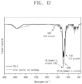
- FIG. 12 is a view illustrating a FTIR spectrum before and after a process of preparing N-TOC-6 through a counter ion exchange reaction of tin oxide [(R 1 Sn) 12 O 14 (OH) 6 ] 2+ (OH ⁇ ) 2 (TOC-6) having a perfluorinated octyl chain (Example 7);
- FIG. 13 is a view illustrating a FTIR spectrum before and after a process of preparing N-TOC-4 through a counter ion exchange reaction of tin oxide [(R 1 Sn) 12 O 14 (OH) 6 ] 2+ (OH ⁇ ) 2 (TOC-4) having a perfluorinated octyl chain (Example 8);
- FIG. 14 is a view illustrating a formation of negative patterns of N-TOC-6 and N-TOC-4 fluorinated tin oxide resists obtained by electron beam lithography according to Examples 9 and 10;
- FIG. 15 is a graph evaluating solubility characteristics of N-TOC-6 and N-TOC-4 fluorinated tin oxide resists obtained by exposing to extreme UV according to Examples 11 and 12;
- FIG. 16 is a view illustrating a formation of negative patterns of N-TOC-6 and N-TOC-4 fluorinated tin oxide resists obtained by performing extreme ultraviolet lithography according to Examples 13 and 14;
- FIG. 17 is a view illustrating a formation of negative patterns of N-TOC-6 and N-TOC-4 fluorinated tin oxide resists obtained by performing extreme ultraviolet lithography including a post-exposure bake (PEB) process according to Examples 15 and 16; and
- PEB post-exposure bake
- FIG. 18 is a graph comparing dry etching rates of N-TOC-6 and N-TOC-4 according to Example 17 as measured.
- resist may also be referred to as ‘photoresist’, ‘electron beam resist’, or ‘extreme ultraviolet resist’.
- a resist material according to example embodiments of the disclosure is an organometallic compound comprising a metal combined with at least one ligand containing four or more fluorine atoms and is represented by the following Chemical Formula 1.
- one of “R 1 ” and “R 2 ” is C a F b H c , C a F b H c N d , C a F b H c P d , C a F b H c S d , C a F b H c O d , C a F b H c N d S e , C a F b H c P d S e , C a F b H c N d O e , or C a F b H c P d O e
- the other of “R 1 ” and “R 2 ” is C a H c , C a F b H c , C a F b H c N d , C a F b H c P d , C a F b H c S d , C a F b H c O d , C a F b H c N
- the organometallic compound may be represented by the following Chemical Formula 1-1.
- the organometallic compound as illustrated in Chemical Formula 1-1 may be stabilized by “q” having a cationic form in which organic ligands “R 1 ” are covalently bonded to metal atoms “M”, and n OH ⁇ groups or p “R 2 ” having the form of an anion.
- M may be tin (Sn), and the organometallic compound may have a structure selected from Chemical Formula 2 to Chemical Formula 5 below.
- Chemical Formula 5 may be expressed as Chemical Formula 5-1 as follows.
- the organometallic compound may have a structure represented by the following Chemical Formula 5-2.
- R 1 may preferably have one structure of
- R 2 may preferably have a structure of
- the organometallic compound may have a spherical cage shape as shown in Chemical Formulas 4, 5, 5-1, and 5-2.
- the organometallic compound includes a tin oxide nanocluster structure having a spherical cage shape in which oxygen atoms and organic ligands “R 1 ” are covalently combined with 12 tin atoms as shown in Chemical Formula 5-1.
- the tin oxide nanocluster structure has a divalent cation.
- the organometallic compound has a structure in which two counter anions are combined with the tin oxide nanocluster structure of divalent cation. As a result, the organometallic compound may be stabilized in an electrically neutral state, generally.
- the organometallic compound has a smaller particle diameter than that of a polymer resin of a chemically amplified resist (CAR) photoresist (PR) and has a uniform size distribution, and thus it is advantageous in terms of securing resolution and line edge roughness (LER), which are performance indicators of a resist pattern.
- CAR chemically amplified resist
- PR photoresist
- the organometallic compound contains four or more fluorine atoms, and thus has very strong hydrophobicity and is resistant to moisture. Accordingly, the resist composition including the organometallic compound may control moisture sensitivity and may have good storage safety. In addition, when the organometallic compound is used as a resist material, process delay (post coating delay [PCD], post exposure delay [PED], post PEB delay [PPD]) may be improved.
- PCD post coating delay
- PED post exposure delay
- PPD post PEB delay
- the organometallic compound may have higher absorbance to extreme ultraviolet (EUV) and have excellent etching resistance in an etching process, and thus may be used as an etching mask.
- the organometallic compound may have a Sn—O—Sn networking structure, and thus may have excellent etching resistance.
- a radical reaction may occur between the organic ligands “R 1 ” as shown in Scheme 1 in a portion exposed to light such as EUV during an exposure process, thereby crosslinking the organometallic compounds. As a result, the molecular weight of the portion exposed to the light increases.
- the organometallic compounds are radical bonded and are not dissolved in a development process.
- a radical reaction may occur even with a small amount of light (a small number of photons), and thus the resist composition according to the disclosure including the organometallic compound as a resist material may have improved photosensitivity.
- a polar ultraviolet is ionizing radiation with a wavelength of 13.5 nm, and an energy of one photon in the polar ultraviolet is 14 times greater than that of a deep ultraviolet ArF excimer laser (193 nm).
- R resolution
- LER line edge roughness
- S sensitivity
- the resist material according to the disclosure is the organometallic compound of Chemical Formula 1, and includes a perfluorinated alkyl chain having excellent absorbance for the extreme ultraviolet, as the organic ligand “R 1 ”.
- the ligand “R 1 ” of the perfluorinated alkyl may form a new cross-linkage between the ligands “R 1 ” because radicals may be formed by high-energy photons in addition to improved absorbance. Thereby, the light sensitivity may be further improved.
- a resist composition according to the disclosure may have improved resolution, mechanical characteristics, and etching resistance.
- the organometallic compound comprising tin with which ligands including four or more fluorine atoms are combined may also be referred to as a ‘fluorinated tin oxide cluster’.
- the fluorinated tin oxide cluster may be developed using a fluorous liquid having a low surface tension and a supercritical CO2 development process. This may prevent collapse of the resist pattern in the development process, thereby implementing accurate patterning without process defects.
- the fluorous liquid may have a low surface tension of preferably 30 dynes/cm to 1 dynes/cm, more preferably 20 dynes/cm to 10 dynes/cm.
- the method for synthesizing the organometallic compound is as follows. First, through a Grignard reaction, perfluoroalkyl triphenyl tin (R 1 SnPh 3 ) containing a perfluorinated alkyl group is prepared (step 1), and is treated with chlorination to synthesize a precursor, perfluoroalkyl tin trichloride (R 1 SnCl 3 ) (step 2). Then, the precursor is hydrolyzed under a basic condition to prepare tin-oxo cage (TOC) nanoclusters in a circular cage shape (step 3). Then, a counter anion of the tin oxide nanocluster is substituted with an anion of a highly fluorinated alkyl ether carboxylic acid to prepare the organometallic compound having the structure of Chemical Formula 1 (Step 4).
- TOC tin-oxo cage
- the solubility of the organometallic compound in the fluorous liquid may be increased. Accordingly, when the resist composition is prepared using the organometallic compound and a resist layer is prepared by spin coating, the resist layer with a thin thickness may be fabricated without defects.
- the resist composition according to the disclosure includes the organometallic compound and an organic solvent.
- the organometallic compound may be included in an amount of 1 to 30 wt. % based on the total weight of the resist composition.
- the organic solvent may be included in an amount of 70 to 99 wt. % based on the total weight of the resist composition.
- the organic solvent may be at least one of propylene glycol monomethyl ether (PGME), propylene glycol monomethyl ether acetate, 2-hydroxyisobutyric acid methyl ester (HBM), ethyl lactate, cyclohexanone, heptanone, lactone, or a fluorine-containing material.
- the organic solvent may be at least one of methyl isobutyl carbinol (MIBC), ether, propylene glycol monomethyl ether acetate (PGMEA), propylene glycol monomethyl ether (PGME), ethyl lactate (EL), ⁇ -hydroxy ⁇ -methylbutyric acid (HBM) or a fluorine-containing material.
- the resist composition may further include a photo acid generator in an amount of 0 to 10 wt. % based on the total weight of the resist composition.
- the photo acid generator is a substance that is decomposed by light to generate a strong acid.
- the generated strong acid may act as a catalyst to control the degree of combination between the organometallic compounds.
- the photo acid generator is preferably at least one of aryldiazonium, diaryliodonium, triarylsulfonium, triarylphosphonium salts, carboxylic acids, sulfonic acids, phosphoric acids, and hydrogen halides.
- the resist composition may further include at least one of a radical quencher, a photolysis quencher, and a base quencher, in an amount of 0 to 10 wt. % based on the total weight of the resist composition.
- the radical quencher, photolysis quencher, and/or base quencher which are substances that cause quenching during the exposure process, may serve to suppress or control hydrogen ions in the resist layer formed of the resist composition.
- the radical quencher, photolysis quencher, and/or base quencher preferably may be at least one of hydrogen chloride, ethyl ester, alcohol, water, a fluorine compound, cyanide, ketone, bromide, oxide, amines, aldehyde, phenol, a nitro compound, and a triarylsulfonium salt.
- the resist composition may further include a thermal acid generator in an amount of 0 to 10 wt. % based on the total weight of the resist composition.
- the thermal acid generator is a substance that is decomposed by heat to generate a strong acid.
- the resist composition may further include a surfactant in an amount of 0 to 10 wt. % based on the total weight of the resist composition.
- a surfactant such as a surfactant from the Sulfinol series by Air Products or the F-series (F-410, F-444, F-477, R-08, R-30) by DIC Corporation (Dainippon Ink Chemical Industry Co., Ltd.) may be used as the surfactant.
- the resist composition may further include at least one of a crosslinking agent, a leveling agent, an antioxidant, and an adhesion improving agent.
- the resist composition according to the disclosure may preferably be a negative resist.
- a method of fabricating a semiconductor device includes preparing a resist composition including an organometallic compound and an organic solvent; forming a resist layer by coating the resist composition on a substrate; performing a soft bake process to evaporate the organic solvent; performing an exposure process to change a portion of the resist layer into a mask pattern; and performing a development process to remove the resist layer while retaining the mask pattern.
- FIG. 1 is a plan view illustrating a resist pattern according to embodiments.
- FIGS. 2 to 5 are diagrams for explaining a method of fabricating a semiconductor device according to embodiments.
- a substrate 100 may be prepared.
- a lower layer 200 and a resist layer 300 may be sequentially formed on the substrate 100 .
- the lower layer 200 may be an etch target layer.
- the lower layer 200 may be formed of any one selected from a semiconductor material, a conductive material, and an insulating material, or a combination thereof.
- the lower layer 200 may be formed as a single layer or may be a plurality of stacked layers. Additional layers may be provided between the substrate 100 and the lower layer 200 .
- a resist composition may be applied on the lower layer 200 to form the resist layer 300 .
- the application of the resist composition may be performed by spin coating.
- a soft bake process may be further performed on the resist composition.
- the soft bake process may be performed at about 80° C. to 200° C. Accordingly, the organic solvent included in the resist layer 300 may be evaporated. ‘Bake’ may be called ‘heating’.
- the soft bake process may be omitted.
- the resist layer 300 may be exposed by a light 500 .
- the light 500 may be an electron beam or extreme ultraviolet.
- a photomask 400 may be disposed on the resist layer 300 .
- the light 500 may be irradiated onto a first portion 310 of the resist layer 300 exposed by the photomask 400 .
- a radical reaction may occur as shown in Scheme 1, and radical bonding between the organometallic compounds of Chemical Formula 1 may occur. Accordingly, a chemical structure of the first portion 310 of the resist layer 300 exposed to the light 500 may be changed.
- a second portion 320 of the resist layer 300 may not be exposed to the light 500 .
- a chemical structure of the second portion 320 of the resist layer 300 may not be changed. Accordingly, after the light 500 is irradiated, the first portion 310 of the resist layer 300 may have a different chemical structure from that of the second portion 320 . Thereafter, the photomask 400 may be removed.
- a post-baking process may be performed after the exposure process.
- the post-bake process (or post-exposure bake process) may be omitted.
- the second portion 320 of the resist layer 300 may be removed by a developer to form a resist pattern 300 P.
- the photoresist pattern 300 P may be formed by a patterning process including exposure and development of the resist layer 300 .
- the resist pattern 300 P may correspond to the first portion 310 of the resist layer 300 .
- the developer may include a high fluorous solution.
- the high fluorous solution may mean a solution having a high fluorine content.
- the developer may include at least one of hydrofluoroether (HFE) and perfluorocarbon (PFC).
- HFE hydrofluoroether
- PFC perfluorocarbon
- the developer may have a low surface tension. Accordingly, pattern collapse of the resist pattern 300 P may be prevented in the development process.
- the development process of the resist pattern 300 P may be chemically stable. Accordingly, the resist pattern 300 P may be formed with a fine width “W” and a pitch.
- the second portion 320 of the resist layer 300 may have high solubility in the developer. As the resist compound has a relatively narrow polydispersity index, the second portion 320 of the resist layer 300 may be uniformly dissolved in the developer. Accordingly, the resist pattern 300 P formed from the resist compound may have a narrow width.
- the resist pattern 300 P may have a linear planar shape.
- the resist pattern 300 P may include portions extending in one direction.
- the planar shape of the resist pattern 300 P may be modified to another shape, such as a zigzag shape, a honeycomb shape, or a circular shape.
- the resist pattern 300 P may expose the lower layer 200 .
- the lower layer 200 exposed by the resist pattern 300 P may be removed to form a lower pattern 200 P.
- the lower layer 200 may be removed by an etching process.
- the lower layer 200 may have etch selectivity with respect to the resist pattern 300 P.
- the lower pattern 200 P may expose the substrate 100 .
- the lower pattern 200 P may expose another layer interposed between the substrate 100 and the lower pattern 200 P.
- the resist pattern 300 P may have strong etching resistance, and thus a shape of the resist pattern 300 P may be maintained during the etching process of the lower layer 200 . Thereafter, the resist pattern 300 P may be removed.
- the lower pattern 200 P may be a gate line or a wiring line of a semiconductor device. Alternatively, the lower pattern 200 P may be a mask pattern in a semiconductor device fabricating process.
- a first solution was prepared by adding magnesium turnings (1.06 g, 43.6 mmol) and diethyl ether (25 cm 3 ) into a 250 cm 3 one-necked round flask at 0° C. After preparing a second solution in which 1H,1H,2H,2H-tridecafluoro-n-octyl iodide (18.6 g, 39.3 mmol) was dissolved in diethyl ether (50 cm 3 ), the second solution was dropped in the first solution cooled with a cooling water bath.
- a fourth solution prepared by dissolving triphenyl tin chloride (5.6 g, 14.53 mmol) in tetrahydrofuran (THF, 25 cm 3 ) was added to the third solution.
- the fourth solution and the third solution were reacted at room temperature for 24 hours to prepare a fifth solution, and purified water (60 cm 3 ) was added to terminate the reaction.
- purified water 60 cm 3
- Perfluorinated octyl triphenyl tin (R 1 SnPh 3 -6) may be synthesized through a Grignard reaction.
- Perfluorinated octyl triphenyl tin (R 1 SnPh 3 -6) or triphenyl(3,3,4,4,5,5,6,6,7,7,8,8,8-tridecafluorooctyl)stannane synthesized according to Example 1 has a structure as shown in Chemical Formula 6 below.
- FIG. 6 is a view illustrating an NMR graph of perfluorinated octyl triphenyl tin (R 1 SnPh 3 -6) synthesized according to Example 1. Referring to FIG. 6 , it may be seen that perfluorinated octyl triphenyl tin (R 1 SnPh 3 -6) is synthesized.
- a first solution was prepared by adding magnesium turnings (0.63 g, 25.9 mmol), 1H,1H,2H,2H-nonafluorohexyl iodide (8.73 g, 23.4 mmol), and diethyl ether (40 cm 3 ) into a 250 cm 3 one-necked round flask at 0° C. After stirring the first solution at room temperature for 3 hours, a second solution prepared by dissolving triphenyl tin chloride (5.0 g, 12.97 mmol) in THF (20 cm 3 ) was added to the first solution.
- Perfluorinated hexyl triphenyl tin (R 1 SnPh 3 -4) may be synthesized through a Grignard reaction.
- Perfluorinated hexyl triphenyl tin (R 1 SnPh 3 -4) or triphenyl(3,3,4,4,5,5,6,6,6-nonafluorohexyl)stannane synthesized according to Example 2 has a structure as shown in Chemical Formula 7 below.
- FIG. 7 is a view illustrating an NMR graph of perfluorinated hexyl triphenyl tin (R 1 SnPh 3 -4) synthesized according to Example 2. Referring to FIG. 7 , it may be seen that perfluorinated hexyl triphenyl tin (R 1 SnPh 3 -4) is synthesized.
- R 1 SnCl 3 -6 was synthesized by chlorination of R 1 SnPh 3 -6 of Example 1.
- R 1 SnPh 3 -6 (3.83 g, 5.50 mmol) of Example 1 and dichloromethane (DCM, 15 cm 3 ) were added and stirred in a 250 cm 3 one-necked round flask to prepare a first solution, and the first solution was cooled to 0° C.
- a second solution (2M concentration, 16.5 cm 3 , 33.0 mmol) of HCl dissolved in diethyl ether was added dropwise to the cooled first solution for 30 minutes, and then a reactant was stirred at room temperature for 12 hours.
- Perfluorinated octyl tin trichloride R 1 SnCl 3 -6) or trichloro(3,3,4,4,5,5,6,6,7,7,8,8,8-tridecafluorooctyl)stannane synthesized according to Example 3 has a structure as shown in Chemical Formula 8 below.
- FIG. 8 is a view illustrating an NMR graph of perfluorinated octyl tin trichloride (R 1 SnCl 3 -6) synthesized according to Example 3. Referring to FIG. 8 , it may be seen that perfluorinated octyl tin trichloride (R 1 SnCl 3 -6) is synthesized.
- a precursor (R 1 SnCl 3 -4) was synthesized by chlorination of R 1 SnPh 3 -4 of Example 2.
- Perfluorinated hexyl tin trichloride R 1 SnCl 3 -4 or trichloro(3,3,4,4,5,5,6,6,6-nonafluorohexyl)stannane synthesized according to Example 4 has a structure as shown in Chemical Formula 9 below.
- FIG. 9 is a view illustrating an NMR graph of perfluorinated hexyl tin trichloride (R 1 SnCl 3 -4) synthesized according to Example 4. Referring to FIG. 9 , it may be seen that perfluorinated hexyl tin trichloride (R 1 SnCl 3 -4) is synthesized.
- Example 3 R 1 SnCl 3 -6 of Example 3 was hydrolyzed under a basic condition to prepare tin-oxo cage (TOC) nanoclusters.
- TOC tin-oxo cage
- R 1 SnCl 3 -6 (2.3 g, 4.02 mmol) of Example 3 was added into a 50 cm 3 vial, and 0.5 M aqueous solution of tetramethylammonium hydroxide (TMAH) (24 cm 3 ) was added with vigorous stirring. The resulting mixture was stirred at room temperature for 1 hour, and then a solid was obtained through a filter. The obtained solid was then washed several times with purified water and dried, and thus a white solid, [(R 1 Sn) 12 O 14 (OH) 6 ] 2+ (OH ⁇ ) 2 (hereinafter referred to as TOC-6) was synthesized (2.09 g, yield: 90%).
- TMAH tetramethylammonium hydroxide
- TOC-6 has a structure of Chemical Formula 5-2, wherein “R 1 ” is as described in Scheme 6.
- FIG. 10 is an NMR graph of a tin-oxo cage [(R 1 Sn) 12 O 14 (OH) 6 ] 2+ (OH ⁇ ) 2 (TOC-6) substituted with a perfluorinated alkyl chain synthesized according to Example 5.
- FIG. 10 it may be seen that [(R 1 Sn) 12 O 14 (OH) 6 ] 2+ (OH ⁇ ) 2 (TOC-6) is synthesized.
- R 1 SnCl 3 -4 of Example 4 was hydrolyzed under a basic condition to prepare tin-oxo cage (TOC) nanoclusters.
- TOC tin-oxo cage
- TOC-4 has the structure of Chemical Formula 5-2, wherein “R 1 ” is as described in Scheme 7.
- FIG. 11 is an NMR graph of a tin-oxo cage [(R 1 Sn) 12 O 14 (OH) 6 ] 2+ (OH ⁇ ) 2 (TOC-4) substituted with a perfluorinated alkyl chain synthesized according to Example 6. Referring to FIG. 11 , it may be seen that [(R 1 Sn) 12 O 14 (OH) 6 ] 2+ (OH ⁇ ) 2 (TOC-4) is synthesized.
- Example 7 Synthesis of tin-oxo cage [(R 1 Sn) 12 O 14 (OH) 6 ] 2+ (CF 3 (CF 2 ) 2 O(CF 3 ) CFCF 2 O(CF 3 )CFCOO ⁇ ) 2 (N-TOC-6) in which a Counter Ion Exchange is Substituted with an Anion of Perfluorinated Alkyl Carboxylic Acid
- N-TOC-6 has a structure of Chemical Formula 5-1 in which two anions (OH—) in TOC-6 of Chemical Formula 5-2 are substituted with “R 2 ” groups.
- the “R 2 ” group may be an anion of perfluorinated alkyl carboxylic acid.
- “R 1 ” is as shown in Scheme 8.
- FIG. 12 is a view illustrating a FTIR spectrum before and after a process of preparing N-TOC-6 through a counter ion exchange reaction of tin oxide [(R 1 Sn) 12 O 14 (OH) 6 ] 2+ (OH ⁇ ) 2 (TOC-6) having a perfluorinated octyl chain (Example 7).
- tin oxide [(R 1 Sn) 12 O 14 (OH) 6 ] 2+ (OH ⁇ ) 2 (TOC-6) having a perfluorinated octyl chain
- Example 8 Synthesis of tin-oxo cage [(R 1 Sn) 12 O 14 (OH) 6 ] 2+ (CF 3 (CF 2 ) 2 O(CF 3 ) CFCF 2 O(CF 3 )CFCOO ⁇ ) 2 (N-TOC-4) in which a Counter Ion Exchange is Substituted with an Anion of Perfluorinated Alkyl Carboxylic Acid
- TOC-4 (0.8 g, 0.17 mmol) of Example 6 was dissolved in THF (3.2 cm 3 ) in a 20 cm 3 vial, and perfluoro(2,5-dimethyl-3,6-dioxanonanoic)acid (0.17 g, 0.34 mmol) was added at room temperature. After stirring the reaction solution at 50° C. for 30 minutes, a reactant was precipitated in hexane twice or three times and filtered.
- N-TOC-4 [(R 1 Sn) 12 O 14 (OH) 6 ] 2+ (CF 3 (CF 2 ) 2 O(CF 3 )CFCF 2 O(CF 3 )CFCOO ⁇ ) 2 (hereinafter referred to as N-TOC-4) was obtained (0.4 g, yield: 50%).
- N-TOC-4 has a structure of Chemical Formula 5-1, in which two anions (OH ⁇ ) in TOC-4 of Chemical Formula 5-2 are substituted with “R 2 ” groups.
- the “R 2 ” group may be an anion of perfluorinated alkyl carboxylic acid.
- “R 1 ” is as shown in Scheme 9.
- FIG. 13 is a view illustrating a FTIR spectrum before and after a process of preparing N-TOC-4 through a counter ion exchange reaction of tin oxide [(R 1 Sn) 12 O 14 (OH) 6 ] 2+ (OH ⁇ ) 2 (TOC-4) having a perfluorinated octyl chain (Example 8).
- N-TOC-4 is synthesized.
- Example 7 A solution of N-TOC-6 (2 wt/vol %) synthesized in Example 7 was dissolved in PF-7600 (3-ethoxy-1,1,1,2,3,4,4,5,5,6,6,6-dodecafluoro-2-trifluoromethyl) (3M Corporation), was spin-coated on a Si substrate primed with vinyltrimethoxysilane (VTMS), at 500 rpm for 60 seconds, and then was heated at 80° C. for 1 minute to form a thin film (approximately 50 nm thick).
- PF-7600 3-ethoxy-1,1,1,2,3,4,4,5,5,6,6,6-dodecafluoro-2-trifluoromethyl
- the thin film was irradiated with an electron beam of 50 to 1,500 ⁇ C/cm 2 under an acceleration voltage of 80 keV, and then a development process was carried out using a mixture of 1,1,1,2,2,3,4,5,5,5-decafluoro-3-methoxy-4-(trifluoromethyl)pentane (HFE-7300) and perfluoro compounds of C5-18 (FC-3283) (1:3) for 5 seconds to form a negative resist pattern with a size of 60 to 100 nm.
- HFE-7300 1,1,1,2,2,3,4,5,5,5-decafluoro-3-methoxy-4-(trifluoromethyl)pentane
- FC-3283 perfluoro compounds of C5-18
- N-TOC-4 (2 wt/vol %) synthesized in Example 8 was dissolved in PF-7600 (1,1,1,2,3,3-Hexafluoro-4-(1,1,2,3,3,3-hexafluoropropoxy)-pentane) (3M Corporation), was spin-coated on a Si substrate primed with vinyltrimethoxysilane (VTMS), at 1,500 rpm for 60 seconds, and then heated at 80° C. for 1 minute to form a thin film (approximately 50 nm thick).
- PF-7600 1,1,1,2,3,3-Hexafluoro-4-(1,1,2,3,3,3-hexafluoropropoxy)-pentane
- the thin film was irradiated with an electron beam of 50 to 1,500 ⁇ C/cm 2 under an acceleration voltage of 80 keV, and then a development process was carried out using PF-7600 for 5 seconds to form a negative resist pattern with a size of 30 to 50 nm.
- FIG. 14 is a view illustrating a formation of negative patterns of N-TOC-6 and N-TOC-4 fluorinated tin oxide resists obtained by electron beam lithography according to Examples 9 and 10. Referring to FIG. 14 , it may be seen that an accurate, fine, and clean line-shaped resist pattern having a 30 nm critical dimension (CD) is formed.
- CD critical dimension
- N-TOC-6 (1.2 wt/vol %) synthesized in Example 7 was dissolved in HFE-7500, was spin-coated on a Si substrate primed with vinyltrimethoxysilane (VTMS), at 1,500 rpm for 60 seconds, and then was heated at 80° C. for 1 minute to form a thin film (approximately 25 nm thick). Thereafter, the thin film was irradiated with extreme ultraviolet (EUV) using an MET5 exposure machine owned by Lawrence Berkeley National Laboratory, and then a development process was carried out using a mixture of HFE-7300 and FC-3283 (1:3) for 20 seconds, and it was confirmed that a negative resist pattern with exposure doses of 1 to 40 mJ/cm 2 was formed. Then, solubility characteristics were evaluated by measuring a thickness through an Alpha-step® D-300 stylus profiler manufactured by KLA-Tencor.
- EUV extreme ultraviolet
- N-TOC-4 (1.3 wt/vol %) synthesized in Example 8 was dissolved in PF-7600, was spin-coated on a Si substrate primed with vinyltrimethoxysilane (VTMS), at 1,500 rpm for 60 seconds, and then was heated at 80° C. for 1 minute to form a thin film (approximately 25 nm thick). Thereafter, the thin film was irradiated with extreme ultraviolet (EUV) using an MET5 exposure machine owned by Lawrence Berkeley National Laboratory, and then a development process was carried out using PF-7600 for 5 seconds, and it was confirmed that a negative resist pattern with exposure doses of 1 to 40 mJ/cm 2 was formed. Then, solubility characteristics were evaluated by measuring a thickness through an Alpha-step® D-300 stylus profiler manufactured by KLA-Tencor.
- EUV extreme ultraviolet
- FIG. 15 is a graph evaluating solubility characteristics of N-TOC-6 and N-TOC-4 fluorinated tin oxide resists obtained by exposing to extreme UV according to Examples 11 and 12. Referring to FIG. 15 , it may be seen that N-TOC-6 and N-TOC-4 have excellent solubility.
- N-TOC-6 synthesized in Example 7 (1.2 wt/vol %) was dissolved in HFE-7500, was spin-coated on a Si substrate primed with vinyltrimethoxysilane (VTMS), at 1,500 rpm for 60 seconds, and then was heated at 80° C. for 1 minute to form a thin film (approximately 25 nm thick).
- VTMS vinyltrimethoxysilane
- the thin film was irradiated with extreme ultraviolet (EUV) using an MET5 exposure machine owned by Lawrence Berkeley National Laboratory, and then a development process was carried out using a mixture of HFE-7300 and FC-3283 (1:3) for 20 seconds, and it was confirmed that a negative resist pattern with reduced solubility at exposure doses (sensitivity) of 10 to 100 mJ/cm 2 was formed.
- EUV extreme ultraviolet
- a solution of N-TOC-4 synthesized in Example 8 (1.3 wt/vol %) was dissolved in PF-7600, was spin-coated on a Si substrate primed with vinyltrimethoxysilane (VTMS), at 1,500 rpm for 60 seconds, and then was heated at 80° C. for 1 minute to form a thin film (approximately 25 nm thick). Thereafter, the thin film was irradiated with extreme ultraviolet (EUV) using an MET5 exposure machine owned by Lawrence Berkeley National Laboratory, and then a development process was carried out using PF-7600 for 5 seconds, and it was confirmed that a negative resist pattern with reduced solubility at exposure doses (sensitivity) of 10 to 100 mJ/cm 2 was formed.
- EUV extreme ultraviolet
- FIG. 16 is a view illustrating a formation of negative patterns of N-TOC-6 and N-TOC-4 fluorinated tin oxide resists obtained by performing extreme ultraviolet lithography according to Examples 13 and 14. Referring to FIG. 16 , it may be seen that an accurate, fine, and clean line-shaped resist pattern having about 9 nm CD is formed.
- a solution of N-TOC-6 synthesized in Example 7 (1.2 wt/vol %) was dissolved in HFE-7500, was spin-coated on a Si substrate primed with vinyltrimethoxysilane (VTMS), at 1,500 rpm for 60 seconds, and then was heated at 80° C. for 1 minute to form a thin film (approximately 25 nm thick). Thereafter, the thin film was irradiated with extreme ultraviolet (EUV) using an MET5 exposure machine owned by Lawrence Berkeley National Laboratory, and then a post-exposure heating process (PEB) was performed at 150° C. for 2 minutes.
- EUV extreme ultraviolet
- a development process was carried out using a mixed solution of HFE-7300 and FC-3283 (3:1) for 5 seconds, and it was confirmed that a negative resist pattern with reduced solubility at exposure doses (sensitivity) of 10 to 100 mJ/cm 2 was formed.
- a solution of N-TOC-4 synthesized in Example 8 (1.3 wt/vol %) was dissolved in PF-7600, was spin-coated on a Si substrate primed with vinyltrimethoxysilane (VTMS), at 1,500 rpm for 60 seconds, and then was heated at 80° C. for 1 minute to form a thin film (approximately 25 nm thick). Thereafter, the thin film was irradiated with extreme ultraviolet (EUV) using an MET5 exposure machine owned by Lawrence Berkeley National Laboratory, and then a post-exposure heating process (PEB) was performed at 150° C. for 2 minutes. A development process was carried out using PF-7600 for 5 seconds, and it was confirmed that a negative resist pattern with reduced solubility at exposure doses (sensitivity) of 10 to 100 mJ/cm 2 was formed.
- EUV extreme ultraviolet
- PEB post-exposure heating process
- FIG. 17 is a view illustrating a formation of negative patterns of N-TOC-6 and N-TOC-4 fluorinated tin oxide resists obtained by performing extreme ultraviolet lithography including a post-exposure bake (PEB) process according to Examples 15 and 16.
- PEB post-exposure bake
- N-TOC-4 thin film with a thickness of 380 nm and an N-TOC-6 thin film with a thickness of 210 nm were formed on the Si substrate primed with vinyltrimethoxysilane (VTMS), respectively.
- VTMS vinyltrimethoxysilane
- a fluorinated organic monomolecular resist [L6, Korean Patent Application No. 10-2019-0016033] having a thickness of 673 nm and a commercial KrF resist having a thickness of 255 nm (provided by Dongjin Semichem) were added.
- the four thin films were put under an RF power of 100 W and a frequency of 100 kHz, and a mixture of 2 sccm of O 2 and 18 sccm of CF 4 which is an etching gas, was added to perform dry etching for 0 to 80 seconds at intervals of 20 seconds. Then, the remaining thin film thickness depending on the drying time was measured using an ellipsometer.
- FIG. 18 is a graph comparing dry etching rates of N-TOC-6 and N-TOC-4 according to Example 17 as measured.
- N-TOC-6 and N-TOC-4 have excellent etching resistance.
- the resist material according to embodiments of the disclosure is the organometallic compound represented by Chemical Formula 1 above.
- the organometallic compound has the structure in which the two counter anions are combined with the tin oxide nanocluster structure of the divalent cations.
- the organometallic compound may be stabilized in the electrically neutral state, generally.
- the organometallic compound has a smaller particle size than that of a polymer resin of a chemically amplified resist (CAR) photoresist (PR) and has a uniform size distribution, and thus it is advantageous in terms of securing resolution, line edge roughness (LER), and line width roughness (LWR), which are the performance indicators of the resist pattern.
- CAR chemically amplified resist
- LWR line width roughness
- the organometallic compound contains the four or more fluorine atoms, and thus has strong hydrophobicity and is resistant to moisture. Accordingly, the resist composition including the organometallic compound has good storage safety.
- the organometallic compound including tin has high absorbance for the extreme ultraviolet and excellent etching resistance. Accordingly, when a pattern is formed using a resist composition including the organometallic compound, a fine, clean and accurate pattern may be formed.
Landscapes
- Chemical & Material Sciences (AREA)
- Organic Chemistry (AREA)
- Physics & Mathematics (AREA)
- General Physics & Mathematics (AREA)
- Engineering & Computer Science (AREA)
- Metallurgy (AREA)
- Materials For Photolithography (AREA)
Abstract
Description
- This application is based on and claims priority under 35 U.S.C. § 119 to Korean Patent Application No. 10-2022-0072386, filed on Jun. 14, 2022, in the Korean Intellectual Property Office, the disclosure of which is incorporated by reference herein in its entirety.
- The disclosure relates to an organometallic compound comprising a metal with which at least one ligand containing four or more fluorine atoms is combined, a resist composition including the same, and a method for fabricating a semiconductor device using the same.
- With development of the semiconductor industry, high integration of a semiconductor device is required, and processing technology for realizing ultra-fine patterns having a line width of 10 nm or less has emerged. The processing technique for forming the patterns has been mainly achieved by a photolithography process using a resist which is a photoresist. The photolithography process forms a resist pattern by forming a resist layer, aligning/exposing a pattern to be formed on the resist layer, and developing the resist layer. The resist applied to form the pattern is largely divided into a negative type resist or a positive type resist. Light sources used in an exposure process include a KrF light source (248 nm), an ArF light source (193 nm), an F2 excimer laser (157 nm), and an extreme ultraviolet (EUV) light source having a wavelength of 13.4 nm.
- One or more embodiments of the disclosure provide a resist material capable of implementing an accurate pattern.
- Further, one or more embodiments of the disclosure provide a resist composition capable of implementing an accurate pattern.
- Further still, one or more embodiments of the disclosure provide a method of fabricating a semiconductor device capable of forming an accurate pattern.
- According to aspect of an example embodiment, a resist material is an organometallic compound comprising a metal combined with at least one ligand containing four or more fluorine atoms and represented by [(R1M)iOjXk(OH)m] (OH)nR2 p, wherein one of “R1” and “R2” is CaFbHc, CaFbHcNd, CaFbHcPd, CaFbHcSd, CaFbHcOd, CaFbHcNdSe, CaFbHcPdSe, CaFbHcNdOe, or CaFbHcPdOe, the other of “R1” and “R2” is CaHc, CaFbHc, CaFbHcNd, CaFbHcPd, CaFbHcSd, CaFbHcOd, CaFbHcNdSe, CaFbHcPdSe, CaFbHcNdOe, or CaFbHcPdOe, “a” is an integer of 1 to 20, “d” and “e” are each independently an integer of 0 to 5, “c” is an integer of 0 to 20, “b” is an integer of 4 to 30, “M” is one metal selected from Sn, Sb, Te, Ir, Ti, Bi, Po, At, In, Ag, Au, Pt, Si, Al, and Ga, “i” is an integer from 1 to 12, “j” is an integer of 1 to 14, “X” is a halogen element selected from I, Cl, F, and Br, “k” is an integer of 0 to 6, “m” is an integer of 0 to 6, “n” is an integer of 0 to 2, and “p” is an integer of 0 to 2.
- According to an aspect of an example embodiment, a resist composition includes an organometallic compound and an organic solvent, wherein the organometallic compound has a structure represented by [(R1M)iOjXk(OH)m] (OH)nR2 p, wherein one of R1 and R2 is CaFbHc, CaFbHcNd, CaFbHcPd, CaFbHcSd, CaFbHcOd, CaFbHcNdSe, CaFbHcPdSe, CaFbHcNdOe, or CaFbHcPdOe, the other of R1 and R2 is CaHc, CaFbHc, CaFbHcNd, CaFbHcPd, CaFbHcSd, CaFbHcOd, CaFbHcNdSe, CaFbHcPdSe, CaFbHcNdOe, or CaFbHcPdOe, a is an integer of 1 to 20, d and e are each independently an integer of 0 to 5, c is an integer of 0 to 20, b is an integer of 4 to 30, M is one metal selected from Sn, Sb, Te, Ir, Ti, Bi, Po, At, In, Ag, Au, Pt, Si, Al, and Ga, i is an integer from 1 to 12, j is an integer of 1 to 14, X is a halogen element selected from I, Cl, F, and Br, k is an integer of 0 to 6, m is an integer of 0 to 6, n is an integer of 0 to 2, and p is an integer of 0 to 2.
- According to an aspect of an example embodiment, a method of fabricating a semiconductor device includes preparing a resist composition including an organometallic compound and an organic solvent, coating the resist composition on a substrate to form a resist layer, performing a soft bake process to evaporate the organic solvent, performing an exposure process and a post-bake process to change a portion of the resist layer into a mask pattern, and performing a development process to remove the resist layer while retaining the mask pattern.
- The above and other aspects, features, and advantages of certain example embodiments of the present disclosure will be more apparent from the following description taken in conjunction with the accompanying drawings, in which:
-
FIG. 1 is a plan view illustrating a resist pattern according to embodiments; -
FIGS. 2 to 5 are diagrams for explaining a method of fabricating a semiconductor device according to embodiments; -
FIG. 6 is a view illustrating an NMR graph of perfluorinated octyl triphenyl tin (R1SnPh3-6) synthesized according to Example 1; -
FIG. 7 is a view illustrating an NMR graph of perfluorinated hexyl triphenyl tin (R1SnPh3-4) synthesized according to Example 2; -
FIG. 8 is a view illustrating an NMR graph of perfluorinated octyl tin trichloride (R1SnCl3-6) synthesized according to Example 3; -
FIG. 9 is a view illustrating an NMR graph of perfluorinated hexyl tin trichloride (R1SnCl3-4) synthesized according to Example 4; -
FIG. 10 is an NMR graph of a tin-oxo cage [(R1Sn)12O14(OH)6]2+(OH−)2 (TOC-6) substituted with a perfluorinated alkyl chain synthesized according to Example 5; -
FIG. 11 is an NMR graph of a tin-oxo cage [(R1Sn)12O14(OH)6]2+(OH−)2 (TOC-4) substituted with a perfluorinated alkyl chain synthesized according to Example 6; -
FIG. 12 is a view illustrating a FTIR spectrum before and after a process of preparing N-TOC-6 through a counter ion exchange reaction of tin oxide [(R1Sn)12O14(OH)6]2+(OH−)2 (TOC-6) having a perfluorinated octyl chain (Example 7); -
FIG. 13 is a view illustrating a FTIR spectrum before and after a process of preparing N-TOC-4 through a counter ion exchange reaction of tin oxide [(R1Sn)12O14(OH)6]2+(OH−)2 (TOC-4) having a perfluorinated octyl chain (Example 8); -
FIG. 14 is a view illustrating a formation of negative patterns of N-TOC-6 and N-TOC-4 fluorinated tin oxide resists obtained by electron beam lithography according to Examples 9 and 10; -
FIG. 15 is a graph evaluating solubility characteristics of N-TOC-6 and N-TOC-4 fluorinated tin oxide resists obtained by exposing to extreme UV according to Examples 11 and 12; -
FIG. 16 is a view illustrating a formation of negative patterns of N-TOC-6 and N-TOC-4 fluorinated tin oxide resists obtained by performing extreme ultraviolet lithography according to Examples 13 and 14; -
FIG. 17 is a view illustrating a formation of negative patterns of N-TOC-6 and N-TOC-4 fluorinated tin oxide resists obtained by performing extreme ultraviolet lithography including a post-exposure bake (PEB) process according to Examples 15 and 16; and -
FIG. 18 is a graph comparing dry etching rates of N-TOC-6 and N-TOC-4 according to Example 17 as measured. - Hereinafter, example embodiments according to the disclosure will be described in detail with reference to the accompanying drawings. In this specification, ‘resist’ may also be referred to as ‘photoresist’, ‘electron beam resist’, or ‘extreme ultraviolet resist’.
- A resist material according to example embodiments of the disclosure is an organometallic compound comprising a metal combined with at least one ligand containing four or more fluorine atoms and is represented by the following Chemical Formula 1.
-
[(R1M)iOjXk(OH)m](OH)nR2 p, (Chemical Formula 1) - In
Chemical Formula 1, one of “R1” and “R2” is CaFbHc, CaFbHcNd, CaFbHcPd, CaFbHcSd, CaFbHcOd, CaFbHcNdSe, CaFbHcPdSe, CaFbHcNdOe, or CaFbHcPdOe, the other of “R1” and “R2” is CaHc, CaFbHc, CaFbHcNd, CaFbHcPd, CaFbHcSd, CaFbHcOd, CaFbHcNdSe, CaFbHcPdSe, CaFbHcNdOe, or CaFbHcPdOe, “a” is an integer of 1 to 20, “d” and “e” are each independently an integer of 0 to 5, “c” is an integer of 0 to 20, “b” is an integer of 4 to 30, “M” is one metal selected from Sn, Sb, Te, Ir, Ti, Bi, Po, At, In, Ag, Au, Pt, Si, Al, and Ga, “i” is an integer from 1 to 12, “j” is an integer of 1 to 14, “X” is a halogen element selected from I, Cl, F, and Br, “k” is an integer of 0 to 6, “m” is an integer of 0 to 6, “n” is an integer of 0 to 2, and “p” is an integer of 0 to 2. “R1” may be referred to as an organic ligand. - The organometallic compound may be represented by the following Chemical Formula 1-1.
-
[(R1M)iOjXk(OH)m]q +(OH−)nR2 p (Chemical Formula 1-1) - In Chemical Formula 1-1, “q” is an integer of 0 to 2. Other symbols are the same as in Chemical Formula 1.
- The organometallic compound as illustrated in Chemical Formula 1-1 may be stabilized by “q” having a cationic form in which organic ligands “R1” are covalently bonded to metal atoms “M”, and n OH− groups or p “R2” having the form of an anion.
- In a preferred embodiment, “M” may be tin (Sn), and the organometallic compound may have a structure selected from Chemical Formula 2 to Chemical Formula 5 below.
-

- Chemical Formula 5 may be expressed as Chemical Formula 5-1 as follows.
-

- The organometallic compound may have a structure represented by the following Chemical Formula 5-2.
-

- “R1” may preferably have one structure of
-

- “R2” may preferably have a structure of
-

- The organometallic compound may have a spherical cage shape as shown in
Chemical Formulas 4, 5, 5-1, and 5-2. - The organometallic compound includes a tin oxide nanocluster structure having a spherical cage shape in which oxygen atoms and organic ligands “R1” are covalently combined with 12 tin atoms as shown in Chemical Formula 5-1. The tin oxide nanocluster structure has a divalent cation. The organometallic compound has a structure in which two counter anions are combined with the tin oxide nanocluster structure of divalent cation. As a result, the organometallic compound may be stabilized in an electrically neutral state, generally. The organometallic compound has a smaller particle diameter than that of a polymer resin of a chemically amplified resist (CAR) photoresist (PR) and has a uniform size distribution, and thus it is advantageous in terms of securing resolution and line edge roughness (LER), which are performance indicators of a resist pattern.
- The organometallic compound contains four or more fluorine atoms, and thus has very strong hydrophobicity and is resistant to moisture. Accordingly, the resist composition including the organometallic compound may control moisture sensitivity and may have good storage safety. In addition, when the organometallic compound is used as a resist material, process delay (post coating delay [PCD], post exposure delay [PED], post PEB delay [PPD]) may be improved.
- When “M” in the organometallic compound is tin, the organometallic compound may have higher absorbance to extreme ultraviolet (EUV) and have excellent etching resistance in an etching process, and thus may be used as an etching mask. The organometallic compound may have a Sn—O—Sn networking structure, and thus may have excellent etching resistance. In the organometallic compound, a radical reaction may occur between the organic ligands “R1” as shown in
Scheme 1 in a portion exposed to light such as EUV during an exposure process, thereby crosslinking the organometallic compounds. As a result, the molecular weight of the portion exposed to the light increases. -

- Accordingly, the organometallic compounds are radical bonded and are not dissolved in a development process. A radical reaction may occur even with a small amount of light (a small number of photons), and thus the resist composition according to the disclosure including the organometallic compound as a resist material may have improved photosensitivity.
- A polar ultraviolet is ionizing radiation with a wavelength of 13.5 nm, and an energy of one photon in the polar ultraviolet is 14 times greater than that of a deep ultraviolet ArF excimer laser (193 nm). As a result, the number of photons injected into EUV lithography is greatly reduced, which leads to an RLS trade-off dilemma among resolution (R), line edge roughness (LER) and sensitivity (S) of the resist pattern. Therefore, it is necessary to maximally absorb the limited number of photons.
- The resist material according to the disclosure is the organometallic compound of
Chemical Formula 1, and includes a perfluorinated alkyl chain having excellent absorbance for the extreme ultraviolet, as the organic ligand “R1”. The ligand “R1” of the perfluorinated alkyl may form a new cross-linkage between the ligands “R1” because radicals may be formed by high-energy photons in addition to improved absorbance. Thereby, the light sensitivity may be further improved. - In addition, a resist composition according to the disclosure may have improved resolution, mechanical characteristics, and etching resistance.
- When the metal “M” is tin, the organometallic compound comprising tin with which ligands including four or more fluorine atoms are combined may also be referred to as a ‘fluorinated tin oxide cluster’. The fluorinated tin oxide cluster may be developed using a fluorous liquid having a low surface tension and a supercritical CO2 development process. This may prevent collapse of the resist pattern in the development process, thereby implementing accurate patterning without process defects. The fluorous liquid may have a low surface tension of preferably 30 dynes/cm to 1 dynes/cm, more preferably 20 dynes/cm to 10 dynes/cm.
- The method for synthesizing the organometallic compound is as follows. First, through a Grignard reaction, perfluoroalkyl triphenyl tin (R1SnPh3) containing a perfluorinated alkyl group is prepared (step 1), and is treated with chlorination to synthesize a precursor, perfluoroalkyl tin trichloride (R1SnCl3) (step 2). Then, the precursor is hydrolyzed under a basic condition to prepare tin-oxo cage (TOC) nanoclusters in a circular cage shape (step 3). Then, a counter anion of the tin oxide nanocluster is substituted with an anion of a highly fluorinated alkyl ether carboxylic acid to prepare the organometallic compound having the structure of Chemical Formula 1 (Step 4).
- By replacing the counter anion with the anion of the highly fluorinated alkyl ether carboxylic acid, the solubility of the organometallic compound in the fluorous liquid may be increased. Accordingly, when the resist composition is prepared using the organometallic compound and a resist layer is prepared by spin coating, the resist layer with a thin thickness may be fabricated without defects.
- The resist composition according to the disclosure includes the organometallic compound and an organic solvent. The organometallic compound may be included in an amount of 1 to 30 wt. % based on the total weight of the resist composition. The organic solvent may be included in an amount of 70 to 99 wt. % based on the total weight of the resist composition.
- Preferably, the organic solvent may be at least one of propylene glycol monomethyl ether (PGME), propylene glycol monomethyl ether acetate, 2-hydroxyisobutyric acid methyl ester (HBM), ethyl lactate, cyclohexanone, heptanone, lactone, or a fluorine-containing material. As another preferable embodiment, the organic solvent may be at least one of methyl isobutyl carbinol (MIBC), ether, propylene glycol monomethyl ether acetate (PGMEA), propylene glycol monomethyl ether (PGME), ethyl lactate (EL), β-hydroxy β-methylbutyric acid (HBM) or a fluorine-containing material.
- In an example, the resist composition may further include a photo acid generator in an amount of 0 to 10 wt. % based on the total weight of the resist composition. The photo acid generator is a substance that is decomposed by light to generate a strong acid. The generated strong acid may act as a catalyst to control the degree of combination between the organometallic compounds. The photo acid generator is preferably at least one of aryldiazonium, diaryliodonium, triarylsulfonium, triarylphosphonium salts, carboxylic acids, sulfonic acids, phosphoric acids, and hydrogen halides.
- In an example, the resist composition may further include at least one of a radical quencher, a photolysis quencher, and a base quencher, in an amount of 0 to 10 wt. % based on the total weight of the resist composition. The radical quencher, photolysis quencher, and/or base quencher, which are substances that cause quenching during the exposure process, may serve to suppress or control hydrogen ions in the resist layer formed of the resist composition. The radical quencher, photolysis quencher, and/or base quencher preferably may be at least one of hydrogen chloride, ethyl ester, alcohol, water, a fluorine compound, cyanide, ketone, bromide, oxide, amines, aldehyde, phenol, a nitro compound, and a triarylsulfonium salt.
- In an example, the resist composition may further include a thermal acid generator in an amount of 0 to 10 wt. % based on the total weight of the resist composition. The thermal acid generator is a substance that is decomposed by heat to generate a strong acid.
- In an example, the resist composition may further include a surfactant in an amount of 0 to 10 wt. % based on the total weight of the resist composition. A commercially available surfactant such as a surfactant from the Sulfinol series by Air Products or the F-series (F-410, F-444, F-477, R-08, R-30) by DIC Corporation (Dainippon Ink Chemical Industry Co., Ltd.) may be used as the surfactant.
- The resist composition may further include at least one of a crosslinking agent, a leveling agent, an antioxidant, and an adhesion improving agent. The resist composition according to the disclosure may preferably be a negative resist.
- A method of fabricating a semiconductor device according to the disclosure includes preparing a resist composition including an organometallic compound and an organic solvent; forming a resist layer by coating the resist composition on a substrate; performing a soft bake process to evaporate the organic solvent; performing an exposure process to change a portion of the resist layer into a mask pattern; and performing a development process to remove the resist layer while retaining the mask pattern.
-
FIG. 1 is a plan view illustrating a resist pattern according to embodiments.FIGS. 2 to 5 are diagrams for explaining a method of fabricating a semiconductor device according to embodiments. - Referring to
FIGS. 1 and 2 , asubstrate 100 may be prepared. Alower layer 200 and a resistlayer 300 may be sequentially formed on thesubstrate 100. Thelower layer 200 may be an etch target layer. Thelower layer 200 may be formed of any one selected from a semiconductor material, a conductive material, and an insulating material, or a combination thereof. In addition, thelower layer 200 may be formed as a single layer or may be a plurality of stacked layers. Additional layers may be provided between thesubstrate 100 and thelower layer 200. - A resist composition may be applied on the
lower layer 200 to form the resistlayer 300. The application of the resist composition may be performed by spin coating. A soft bake process may be further performed on the resist composition. The soft bake process may be performed at about 80° C. to 200° C. Accordingly, the organic solvent included in the resistlayer 300 may be evaporated. ‘Bake’ may be called ‘heating’. The soft bake process may be omitted. - Referring to
FIGS. 1 and 3 , the resistlayer 300 may be exposed by a light 500. The light 500 may be an electron beam or extreme ultraviolet. Before the light 500 is irradiated, aphotomask 400 may be disposed on the resistlayer 300. The light 500 may be irradiated onto afirst portion 310 of the resistlayer 300 exposed by thephotomask 400. When the resistlayer 300 is exposed to the light 500, a radical reaction may occur as shown inScheme 1, and radical bonding between the organometallic compounds ofChemical Formula 1 may occur. Accordingly, a chemical structure of thefirst portion 310 of the resistlayer 300 exposed to the light 500 may be changed. - A
second portion 320 of the resistlayer 300 may not be exposed to the light 500. A chemical structure of thesecond portion 320 of the resistlayer 300 may not be changed. Accordingly, after the light 500 is irradiated, thefirst portion 310 of the resistlayer 300 may have a different chemical structure from that of thesecond portion 320. Thereafter, thephotomask 400 may be removed. - A post-baking process may be performed after the exposure process. The post-bake process (or post-exposure bake process) may be omitted.
- Referring to
FIGS. 1 and 4 , thesecond portion 320 of the resistlayer 300 may be removed by a developer to form a resistpattern 300P. Thephotoresist pattern 300P may be formed by a patterning process including exposure and development of the resistlayer 300. The resistpattern 300P may correspond to thefirst portion 310 of the resistlayer 300. The developer may include a high fluorous solution. The high fluorous solution may mean a solution having a high fluorine content. For example, the developer may include at least one of hydrofluoroether (HFE) and perfluorocarbon (PFC). When the high fluorous solution is used as the developer, the developer may have a low surface tension. Accordingly, pattern collapse of the resistpattern 300P may be prevented in the development process. The development process of the resistpattern 300P may be chemically stable. Accordingly, the resistpattern 300P may be formed with a fine width “W” and a pitch. - The
second portion 320 of the resistlayer 300 may have high solubility in the developer. As the resist compound has a relatively narrow polydispersity index, thesecond portion 320 of the resistlayer 300 may be uniformly dissolved in the developer. Accordingly, the resistpattern 300P formed from the resist compound may have a narrow width. - As shown in
FIG. 1 , the resistpattern 300P may have a linear planar shape. For example, the resistpattern 300P may include portions extending in one direction. However, the planar shape of the resistpattern 300P may be modified to another shape, such as a zigzag shape, a honeycomb shape, or a circular shape. The resistpattern 300P may expose thelower layer 200. - Referring to
FIGS. 1 and 5 , thelower layer 200 exposed by the resistpattern 300P may be removed to form alower pattern 200P. Thelower layer 200 may be removed by an etching process. Thelower layer 200 may have etch selectivity with respect to the resistpattern 300P. Thelower pattern 200P may expose thesubstrate 100. As another example, thelower pattern 200P may expose another layer interposed between thesubstrate 100 and thelower pattern 200P. - The resist
pattern 300P may have strong etching resistance, and thus a shape of the resistpattern 300P may be maintained during the etching process of thelower layer 200. Thereafter, the resistpattern 300P may be removed. Thelower pattern 200P may be a gate line or a wiring line of a semiconductor device. Alternatively, thelower pattern 200P may be a mask pattern in a semiconductor device fabricating process. - Hereinafter, embodiments of the disclosure will be described in detail.
- A first solution was prepared by adding magnesium turnings (1.06 g, 43.6 mmol) and diethyl ether (25 cm3) into a 250 cm3 one-necked round flask at 0° C. After preparing a second solution in which 1H,1H,2H,2H-tridecafluoro-n-octyl iodide (18.6 g, 39.3 mmol) was dissolved in diethyl ether (50 cm3), the second solution was dropped in the first solution cooled with a cooling water bath. After removing the cooling water bath and stirring a third solution formed by a reaction of the first solution and the second solution at room temperature for 3 hours, a fourth solution prepared by dissolving triphenyl tin chloride (5.6 g, 14.53 mmol) in tetrahydrofuran (THF, 25 cm3) was added to the third solution. The fourth solution and the third solution were reacted at room temperature for 24 hours to prepare a fifth solution, and purified water (60 cm3) was added to terminate the reaction. After filtering the fifth solution through Celite, a product was extracted from the fifth solution with hexane, and the product was washed with water and a saturated aqueous sodium chloride solution. Anhydrous MgSO4 was added to an organic liquid separated from the fifth solution, followed by stirring to remove moisture in the product. After filtration, the organic liquid obtained by concentration under reduced pressure was purified through column chromatography (silica gel, hexane), and thus a white solid, triphenyl(3,3,4,4,5,5,6,6,7,7,8,8,8-tridecafluorooctyl)stannane (R1SnPh3-6) was obtained (6.73 g, yield: 67%).
- 1H NMR (400 MHz, acetone, ppm): δ=7.37-7.71 (m, 10H), 2.24-2.49 (t+q, 2H, J=16, 20 MHz), 1.74 (t, 2H, J=8 Hz))
- Perfluorinated octyl triphenyl tin (R1SnPh3-6) may be synthesized through a Grignard reaction.
- A chemical reaction according to Example 1 is shown in
Scheme 2 below. -

- Perfluorinated octyl triphenyl tin (R1SnPh3-6) or triphenyl(3,3,4,4,5,5,6,6,7,7,8,8,8-tridecafluorooctyl)stannane synthesized according to Example 1 has a structure as shown in
Chemical Formula 6 below. -

-
FIG. 6 is a view illustrating an NMR graph of perfluorinated octyl triphenyl tin (R1SnPh3-6) synthesized according to Example 1. Referring toFIG. 6 , it may be seen that perfluorinated octyl triphenyl tin (R1SnPh3-6) is synthesized. - A first solution was prepared by adding magnesium turnings (0.63 g, 25.9 mmol), 1H,1H,2H,2H-nonafluorohexyl iodide (8.73 g, 23.4 mmol), and diethyl ether (40 cm3) into a 250 cm3 one-necked round flask at 0° C. After stirring the first solution at room temperature for 3 hours, a second solution prepared by dissolving triphenyl tin chloride (5.0 g, 12.97 mmol) in THF (20 cm3) was added to the first solution. After the first solution and the second solution were reacted at room temperature for 24 hours to prepare a third solution, and purified water (60 cm3) was added to terminate the reaction. After filtering the third solution through Celite, a product was extracted from the third solution with hexane (60 cm3), and the product was washed with water and a saturated aqueous sodium chloride solution. Anhydrous MgSO4 was added to an organic liquid separated from the third solution, followed by stirring to remove moisture in the product. After filtration, the organic liquid obtained by concentration under reduced pressure was purified through chromatography (silica gel, hexane), and a white solid, triphenyl(3,3,4,4,5,5,6,6,6-nonafluorohexyl)stannane (R1SnPh3-4, 6.0 g yield: 71%) was obtained.
- 1H NMR (400 MHz, CDCl3, ppm): δ=7.35-7.60 (m, 15H), 2.25-2.44 (t+q, 2H, J=16.4 Hz, 17.2 Hz), 1.50-1.69 (t+q, 2H), J=17.6 Hz, 19.6 Hz)
- Perfluorinated hexyl triphenyl tin (R1SnPh3-4) may be synthesized through a Grignard reaction.
- A chemical reaction according to Example 2 is shown in Scheme 3 below.
-

- Perfluorinated hexyl triphenyl tin (R1SnPh3-4) or triphenyl(3,3,4,4,5,5,6,6,6-nonafluorohexyl)stannane synthesized according to Example 2 has a structure as shown in Chemical Formula 7 below.
-

-
FIG. 7 is a view illustrating an NMR graph of perfluorinated hexyl triphenyl tin (R1SnPh3-4) synthesized according to Example 2. Referring toFIG. 7 , it may be seen that perfluorinated hexyl triphenyl tin (R1SnPh3-4) is synthesized. - A precursor, R1SnCl3-6, was synthesized by chlorination of R1SnPh3-6 of Example 1. In detail, R1SnPh3-6 (3.83 g, 5.50 mmol) of Example 1 and dichloromethane (DCM, 15 cm3) were added and stirred in a 250 cm3 one-necked round flask to prepare a first solution, and the first solution was cooled to 0° C. A second solution (2M concentration, 16.5 cm3, 33.0 mmol) of HCl dissolved in diethyl ether was added dropwise to the cooled first solution for 30 minutes, and then a reactant was stirred at room temperature for 12 hours. After evaporating a solvent from the reactant under reduced pressure, the reactant was purified using Kugelrohr distillation, and thus a transparent liquid, trichloro(3,3,4,4,5,5,6,6,7,7,8,8,8-tridecafluorooctyl)stannane (R1SnCl3-6) was obtained (1.45 g, yield: 46%).
- 1H NMR (400 MHz, CDCl3, ppm): δ=2.69 (sep, 2H, J=8 Hz), 2.37 (t, 2H, J=8 Hz)
- A chemical reaction according to Example 3 is shown in
Scheme 4 below. -

- Perfluorinated octyl tin trichloride (R1SnCl3-6) or trichloro(3,3,4,4,5,5,6,6,7,7,8,8,8-tridecafluorooctyl)stannane synthesized according to Example 3 has a structure as shown in Chemical Formula 8 below.
-

-
FIG. 8 is a view illustrating an NMR graph of perfluorinated octyl tin trichloride (R1SnCl3-6) synthesized according to Example 3. Referring toFIG. 8 , it may be seen that perfluorinated octyl tin trichloride (R1SnCl3-6) is synthesized. - A precursor (R1SnCl3-4) was synthesized by chlorination of R1SnPh3-4 of Example 2.
- R1SnPh3-4 (5.5 g, 9.22 mmol) and dichloromethane (DCM, 20 cm3) of Example 2 were added into a 100 cm3 one-necked round flask, and then cooled to 0° C. to prepare a first solution. Thereafter, a second solution (2M concentration, 27.7 cm3, 55.4 mmol) of HCl dissolved in diethyl ether was added dropwise to the first solution over 30 minutes. A reactant was stirred at 35° C. for 12 hours, and then was concentrated under reduced pressure. This was distilled at 200° C. under reduced pressure, and a pale yellow liquid, trichloro(3,3,4,4,5,5,6,6,6-nonafluorohexyl)stannane (R1SnCl3-4) was obtained (2.8 g, yield: 64%).
- 1H NMR (400 MHz, CDCl3, ppm): δ=2.55-2.73 (m, 2H), 2.25-2.36 (t, 2H, J=8 Hz)
- A chemical reaction according to Example 4 is shown in Scheme 5 below.
-

- Perfluorinated hexyl tin trichloride (R1SnCl3-4) or trichloro(3,3,4,4,5,5,6,6,6-nonafluorohexyl)stannane synthesized according to Example 4 has a structure as shown in Chemical Formula 9 below.
-

-
FIG. 9 is a view illustrating an NMR graph of perfluorinated hexyl tin trichloride (R1SnCl3-4) synthesized according to Example 4. Referring toFIG. 9 , it may be seen that perfluorinated hexyl tin trichloride (R1SnCl3-4) is synthesized. - R1SnCl3-6 of Example 3 was hydrolyzed under a basic condition to prepare tin-oxo cage (TOC) nanoclusters.
- R1SnCl3-6 (2.3 g, 4.02 mmol) of Example 3 was added into a 50 cm3 vial, and 0.5 M aqueous solution of tetramethylammonium hydroxide (TMAH) (24 cm3) was added with vigorous stirring. The resulting mixture was stirred at room temperature for 1 hour, and then a solid was obtained through a filter. The obtained solid was then washed several times with purified water and dried, and thus a white solid, [(R1Sn)12O14(OH)6]2+(OH−)2 (hereinafter referred to as TOC-6) was synthesized (2.09 g, yield: 90%).
- 1H NMR (400 MHz, acetone, ppm): δ=2.34-2.84 (br, 2H), 0.78-1.57 (br, 2H) IR [(KBR): v_max, (cm{circumflex over ( )}(−1))] 1242, 1209, 1142, 734. 702, 656, 559, 518
- m/z (MALDI-TOF) 5964.518 [Exact mass: 5962.90 for C96H56F156O22Sn12]
- A chemical reaction according to Example 5 is shown in
Scheme 6 below -

- TOC-6 has a structure of Chemical Formula 5-2, wherein “R1” is as described in
Scheme 6. -
FIG. 10 is an NMR graph of a tin-oxo cage [(R1Sn)12O14(OH)6]2+(OH−)2 (TOC-6) substituted with a perfluorinated alkyl chain synthesized according to Example 5. Referring toFIG. 10 , it may be seen that [(R1Sn)12O14(OH)6]2+(OH−)2 (TOC-6) is synthesized. - R1SnCl3-4 of Example 4 was hydrolyzed under a basic condition to prepare tin-oxo cage (TOC) nanoclusters.
- After dissolving tetramethylammonium hydroxide pentahydrate (TMAH, 3.22 g, 17.8 mmol) in purified water (35.5 cm3) in a 50 cm3 vial, R1SnCl3-4 (2.5 g, 5.29 mmol) of Example 4 was quickly added. The reaction solution was stirred vigorously at room temperature for 1 hour, and then an obtained product was filtered. The solid was washed with purified water several times and then dried under vacuum, and a white solid, [(R1Sn)12O14(OH)6]2+(OH−)2 (hereinafter referred to as TOC-4) was obtained (1.6 g, yield: 64%).
- 1H NMR (400 MHz, (CD3)CO, ppm): δ=2.29-2.90 (br, 24H), 0.84-1.52 (br, 24H)
- IR [(KBr): v_max, (cm{circumflex over ( )}(−1))] 3355, 2938, 1491, 1447, 1346, 1224, 1134, 1063, 1010, 881, 839, 731, 572, 520
- A chemical reaction according to Example 6 is shown in Scheme 7 below.
-

- TOC-4 has the structure of Chemical Formula 5-2, wherein “R1” is as described in Scheme 7.
-
FIG. 11 is an NMR graph of a tin-oxo cage [(R1Sn)12O14(OH)6]2+(OH−)2 (TOC-4) substituted with a perfluorinated alkyl chain synthesized according to Example 6. Referring toFIG. 11 , it may be seen that [(R1Sn)12O14(OH)6]2+(OH−)2 (TOC-4) is synthesized. - After adding TOC-6 (1 g, 0.16 mmol) and tetrahydrofuran (THF, 4 cm3) of Example 5 into a 50 cm3 vial and stirring, perfluoro(2,5-dimethyl-3,6-dioxanonaic)acid (0.16 g, 0.33 mmol) was added. The resulting mixture was stirred at 50° C. for 30 minutes, and then a reactant was concentrated under reduced pressure to obtain a product in a form of a viscous liquid. Thereafter, a precipitation process of dissolving the product in trifluorotoluene (3 cm3) and dropping the product into toluene was repeated twice, and a solid precipitate was obtained and dried, and thus a white solid, CF3(CF2)2O(CF3)CFCF2O(CF3)CFCOO−)2 (hereinafter referred to as N-TOC-6) was obtained (0.488 g, yield: 48%).
- IR [(KBR): v_max, (cm{circumflex over ( )}(−1))] 1667, 1242, 1209, 1142, 734.702, 656, 559, 518
- A chemical reaction according to Example 7 is shown in Scheme 8 below.
-

- N-TOC-6 has a structure of Chemical Formula 5-1 in which two anions (OH—) in TOC-6 of Chemical Formula 5-2 are substituted with “R2” groups. The “R2” group may be an anion of perfluorinated alkyl carboxylic acid. In N-TOC-6, “R1” is as shown in Scheme 8.
-
FIG. 12 is a view illustrating a FTIR spectrum before and after a process of preparing N-TOC-6 through a counter ion exchange reaction of tin oxide [(R1Sn)12O14(OH)6]2+(OH−)2 (TOC-6) having a perfluorinated octyl chain (Example 7). Referring toFIG. 12 , it may be seen that N-TOC-6 is synthesized. - TOC-4 (0.8 g, 0.17 mmol) of Example 6 was dissolved in THF (3.2 cm3) in a 20 cm3 vial, and perfluoro(2,5-dimethyl-3,6-dioxanonanoic)acid (0.17 g, 0.34 mmol) was added at room temperature. After stirring the reaction solution at 50° C. for 30 minutes, a reactant was precipitated in hexane twice or three times and filtered. After vacuum drying, a white solid final material, [(R1Sn)12O14(OH)6]2+(CF3(CF2)2O(CF3)CFCF2O(CF3)CFCOO−)2 (hereinafter referred to as N-TOC-4) was obtained (0.4 g, yield: 50%).
- 1H NMR (400 MHz, CDOD, ppm): δ=2.33-2.76 (br, 24H), 1.45-1.70 (br, 24H)
- IR [(KBr): v_max, (cm{circumflex over ( )}(−1))] 1664, 1491, 1447, 1346, 1224, 1134, 1063, 995, 881, 839, 731, 572, 520
- m/z (MALDI-TOF) 5765.09 [Exact mass: 5707.68 for C114H54Sn12O26F190, 5781.82 for M+(Me)4N+]
- A chemical reaction according to Example 8 is shown in Scheme 9 below.
-

- N-TOC-4 has a structure of Chemical Formula 5-1, in which two anions (OH−) in TOC-4 of Chemical Formula 5-2 are substituted with “R2” groups. The “R2” group may be an anion of perfluorinated alkyl carboxylic acid. In N-TOC-4, “R1” is as shown in Scheme 9.
-
FIG. 13 is a view illustrating a FTIR spectrum before and after a process of preparing N-TOC-4 through a counter ion exchange reaction of tin oxide [(R1Sn)12O14(OH)6]2+(OH−)2 (TOC-4) having a perfluorinated octyl chain (Example 8). Referring toFIG. 13 , it may be seen that N-TOC-4 is synthesized. - A solution of N-TOC-6 (2 wt/vol %) synthesized in Example 7 was dissolved in PF-7600 (3-ethoxy-1,1,1,2,3,4,4,5,5,6,6,6-dodecafluoro-2-trifluoromethyl) (3M Corporation), was spin-coated on a Si substrate primed with vinyltrimethoxysilane (VTMS), at 500 rpm for 60 seconds, and then was heated at 80° C. for 1 minute to form a thin film (approximately 50 nm thick). Thereafter, the thin film was irradiated with an electron beam of 50 to 1,500 μC/cm2 under an acceleration voltage of 80 keV, and then a development process was carried out using a mixture of 1,1,1,2,2,3,4,5,5,5-decafluoro-3-methoxy-4-(trifluoromethyl)pentane (HFE-7300) and perfluoro compounds of C5-18 (FC-3283) (1:3) for 5 seconds to form a negative resist pattern with a size of 60 to 100 nm.
- A solution of N-TOC-4 (2 wt/vol %) synthesized in Example 8 was dissolved in PF-7600 (1,1,1,2,3,3-Hexafluoro-4-(1,1,2,3,3,3-hexafluoropropoxy)-pentane) (3M Corporation), was spin-coated on a Si substrate primed with vinyltrimethoxysilane (VTMS), at 1,500 rpm for 60 seconds, and then heated at 80° C. for 1 minute to form a thin film (approximately 50 nm thick). Thereafter, the thin film was irradiated with an electron beam of 50 to 1,500 μC/cm2 under an acceleration voltage of 80 keV, and then a development process was carried out using PF-7600 for 5 seconds to form a negative resist pattern with a size of 30 to 50 nm.
-
FIG. 14 is a view illustrating a formation of negative patterns of N-TOC-6 and N-TOC-4 fluorinated tin oxide resists obtained by electron beam lithography according to Examples 9 and 10. Referring toFIG. 14 , it may be seen that an accurate, fine, and clean line-shaped resist pattern having a 30 nm critical dimension (CD) is formed. - A solution of N-TOC-6 (1.2 wt/vol %) synthesized in Example 7 was dissolved in HFE-7500, was spin-coated on a Si substrate primed with vinyltrimethoxysilane (VTMS), at 1,500 rpm for 60 seconds, and then was heated at 80° C. for 1 minute to form a thin film (approximately 25 nm thick). Thereafter, the thin film was irradiated with extreme ultraviolet (EUV) using an MET5 exposure machine owned by Lawrence Berkeley National Laboratory, and then a development process was carried out using a mixture of HFE-7300 and FC-3283 (1:3) for 20 seconds, and it was confirmed that a negative resist pattern with exposure doses of 1 to 40 mJ/cm2 was formed. Then, solubility characteristics were evaluated by measuring a thickness through an Alpha-step® D-300 stylus profiler manufactured by KLA-Tencor.
- A solution of N-TOC-4 (1.3 wt/vol %) synthesized in Example 8 was dissolved in PF-7600, was spin-coated on a Si substrate primed with vinyltrimethoxysilane (VTMS), at 1,500 rpm for 60 seconds, and then was heated at 80° C. for 1 minute to form a thin film (approximately 25 nm thick). Thereafter, the thin film was irradiated with extreme ultraviolet (EUV) using an MET5 exposure machine owned by Lawrence Berkeley National Laboratory, and then a development process was carried out using PF-7600 for 5 seconds, and it was confirmed that a negative resist pattern with exposure doses of 1 to 40 mJ/cm2 was formed. Then, solubility characteristics were evaluated by measuring a thickness through an Alpha-step® D-300 stylus profiler manufactured by KLA-Tencor.
-
FIG. 15 is a graph evaluating solubility characteristics of N-TOC-6 and N-TOC-4 fluorinated tin oxide resists obtained by exposing to extreme UV according to Examples 11 and 12. Referring toFIG. 15 , it may be seen that N-TOC-6 and N-TOC-4 have excellent solubility. - A solution of N-TOC-6 synthesized in Example 7 (1.2 wt/vol %) was dissolved in HFE-7500, was spin-coated on a Si substrate primed with vinyltrimethoxysilane (VTMS), at 1,500 rpm for 60 seconds, and then was heated at 80° C. for 1 minute to form a thin film (approximately 25 nm thick). Thereafter, the thin film was irradiated with extreme ultraviolet (EUV) using an MET5 exposure machine owned by Lawrence Berkeley National Laboratory, and then a development process was carried out using a mixture of HFE-7300 and FC-3283 (1:3) for 20 seconds, and it was confirmed that a negative resist pattern with reduced solubility at exposure doses (sensitivity) of 10 to 100 mJ/cm2 was formed.
- A solution of N-TOC-4 synthesized in Example 8 (1.3 wt/vol %) was dissolved in PF-7600, was spin-coated on a Si substrate primed with vinyltrimethoxysilane (VTMS), at 1,500 rpm for 60 seconds, and then was heated at 80° C. for 1 minute to form a thin film (approximately 25 nm thick). Thereafter, the thin film was irradiated with extreme ultraviolet (EUV) using an MET5 exposure machine owned by Lawrence Berkeley National Laboratory, and then a development process was carried out using PF-7600 for 5 seconds, and it was confirmed that a negative resist pattern with reduced solubility at exposure doses (sensitivity) of 10 to 100 mJ/cm2 was formed.
-
FIG. 16 is a view illustrating a formation of negative patterns of N-TOC-6 and N-TOC-4 fluorinated tin oxide resists obtained by performing extreme ultraviolet lithography according to Examples 13 and 14. Referring toFIG. 16 , it may be seen that an accurate, fine, and clean line-shaped resist pattern having about 9 nm CD is formed. - A solution of N-TOC-6 synthesized in Example 7 (1.2 wt/vol %) was dissolved in HFE-7500, was spin-coated on a Si substrate primed with vinyltrimethoxysilane (VTMS), at 1,500 rpm for 60 seconds, and then was heated at 80° C. for 1 minute to form a thin film (approximately 25 nm thick). Thereafter, the thin film was irradiated with extreme ultraviolet (EUV) using an MET5 exposure machine owned by Lawrence Berkeley National Laboratory, and then a post-exposure heating process (PEB) was performed at 150° C. for 2 minutes. A development process was carried out using a mixed solution of HFE-7300 and FC-3283 (3:1) for 5 seconds, and it was confirmed that a negative resist pattern with reduced solubility at exposure doses (sensitivity) of 10 to 100 mJ/cm2 was formed.
- A solution of N-TOC-4 synthesized in Example 8 (1.3 wt/vol %) was dissolved in PF-7600, was spin-coated on a Si substrate primed with vinyltrimethoxysilane (VTMS), at 1,500 rpm for 60 seconds, and then was heated at 80° C. for 1 minute to form a thin film (approximately 25 nm thick). Thereafter, the thin film was irradiated with extreme ultraviolet (EUV) using an MET5 exposure machine owned by Lawrence Berkeley National Laboratory, and then a post-exposure heating process (PEB) was performed at 150° C. for 2 minutes. A development process was carried out using PF-7600 for 5 seconds, and it was confirmed that a negative resist pattern with reduced solubility at exposure doses (sensitivity) of 10 to 100 mJ/cm2 was formed.
-
FIG. 17 is a view illustrating a formation of negative patterns of N-TOC-6 and N-TOC-4 fluorinated tin oxide resists obtained by performing extreme ultraviolet lithography including a post-exposure bake (PEB) process according to Examples 15 and 16. Referring toFIG. 17 , it may be seen that an accurate, fine, and clean line-shaped resist pattern having about 9 nm CD is formed. - An N-TOC-4 thin film with a thickness of 380 nm and an N-TOC-6 thin film with a thickness of 210 nm were formed on the Si substrate primed with vinyltrimethoxysilane (VTMS), respectively. For comparison of etching resistance according to metal content, a fluorinated organic monomolecular resist [L6, Korean Patent Application No. 10-2019-0016033] having a thickness of 673 nm and a commercial KrF resist having a thickness of 255 nm (provided by Dongjin Semichem) were added. Thereafter, the four thin films were put under an RF power of 100 W and a frequency of 100 kHz, and a mixture of 2 sccm of O2 and 18 sccm of CF4 which is an etching gas, was added to perform dry etching for 0 to 80 seconds at intervals of 20 seconds. Then, the remaining thin film thickness depending on the drying time was measured using an ellipsometer.
-
FIG. 18 is a graph comparing dry etching rates of N-TOC-6 and N-TOC-4 according to Example 17 as measured. - Referring to
FIG. 18 , according to Example 17, the thicknesses of N-TOC-6 and N-TOC-4 hardly change regardless of time. Accordingly, it may be seen that N-TOC-6 and N-TOC-4 have excellent etching resistance. - The resist material according to embodiments of the disclosure is the organometallic compound represented by
Chemical Formula 1 above. The organometallic compound has the structure in which the two counter anions are combined with the tin oxide nanocluster structure of the divalent cations. Thus, the organometallic compound may be stabilized in the electrically neutral state, generally. The organometallic compound has a smaller particle size than that of a polymer resin of a chemically amplified resist (CAR) photoresist (PR) and has a uniform size distribution, and thus it is advantageous in terms of securing resolution, line edge roughness (LER), and line width roughness (LWR), which are the performance indicators of the resist pattern. - The organometallic compound contains the four or more fluorine atoms, and thus has strong hydrophobicity and is resistant to moisture. Accordingly, the resist composition including the organometallic compound has good storage safety.
- The organometallic compound including tin has high absorbance for the extreme ultraviolet and excellent etching resistance. Accordingly, when a pattern is formed using a resist composition including the organometallic compound, a fine, clean and accurate pattern may be formed.
- While embodiments are described above, a person skilled in the art may understand that many modifications and variations are made without departing from the spirit and scope of the disclosure defined in the following claims. Accordingly, the example embodiments of the disclosure should be considered in all respects as illustrative and not restrictive, with the spirit and scope of the disclosure being indicated by the appended claims.
Claims (20)
[(R1M)iOjXk(OH)m](OH)nR2 p, (Chemical Formula 1)


[(R1M)iOjXk(OH)m](OH)nR2 p, (Chemical Formula 1)


[(R1M)iOjXk(OH)m](OH)nR2 p, (Chemical Formula 1)


Applications Claiming Priority (2)
| Application Number | Priority Date | Filing Date | Title |
|---|---|---|---|
| KR1020220072386A KR20230172078A (en) | 2022-06-14 | 2022-06-14 | Organometallic compound combined with ligands containing 4 or more fluorine atoms, Resist composition comprising the same, and method of fabricating a semiconductor device using the same |
| KR10-2022-0072386 | 2022-06-14 |
Publications (2)
| Publication Number | Publication Date |
|---|---|
| US20230400764A1 true US20230400764A1 (en) | 2023-12-14 |
| US12693595B2 US12693595B2 (en) | 2026-07-28 |
Family
ID=89077318
Family Applications (1)
| Application Number | Title | Priority Date | Filing Date |
|---|---|---|---|
| US18/120,248 Active 2044-11-08 US12693595B2 (en) | 2022-06-14 | 2023-03-10 | Organometallic compound comprising a metal combined with at least one ligand containing four or more fluorine atoms, resist composition comprising the same, and method of fabricating semiconductor device using the same |
Country Status (2)
| Country | Link |
|---|---|
| US (1) | US12693595B2 (en) |
| KR (1) | KR20230172078A (en) |
Family Cites Families (16)
| Publication number | Priority date | Publication date | Assignee | Title |
|---|---|---|---|---|
| US8366967B2 (en) | 2010-02-22 | 2013-02-05 | Inpria Corporation | Metal chalcogenide aqueous precursors and processes to form metal chalcogenide films |
| US9176377B2 (en) | 2010-06-01 | 2015-11-03 | Inpria Corporation | Patterned inorganic layers, radiation based patterning compositions and corresponding methods |
| WO2012118847A2 (en) | 2011-02-28 | 2012-09-07 | Inpria Corportion | Solution processible hardmarks for high resolusion lithography |
| US8710497B2 (en) | 2011-12-08 | 2014-04-29 | LG Dispay Co., Ltd | Array substrate including thin film transistor and method of fabricating the same |
| US9310684B2 (en) | 2013-08-22 | 2016-04-12 | Inpria Corporation | Organometallic solution based high resolution patterning compositions |
| GB201517273D0 (en) | 2015-09-30 | 2015-11-11 | Univ Manchester | Resist composition |
| KR102708400B1 (en) * | 2015-10-13 | 2024-09-20 | 인프리아 코포레이션 | Organotin oxide hydroxide patterning compositions, precursors, and patterning |
| WO2018123537A1 (en) | 2016-12-28 | 2018-07-05 | Jsr株式会社 | Radiation sensitive composition, pattern forming method and metal oxide |
| TWI778248B (en) | 2018-04-05 | 2022-09-21 | 美商英培雅股份有限公司 | Tin dodecamers and radiation patternable coatings with strong euv absorption |
| US11054742B2 (en) * | 2018-06-15 | 2021-07-06 | Taiwan Semiconductor Manufacturing Co., Ltd. | EUV metallic resist performance enhancement via additives |
| KR102287507B1 (en) | 2018-08-16 | 2021-08-09 | 삼성에스디아이 주식회사 | Hardmask composition and method of forming patterns |
| KR102215511B1 (en) | 2019-02-12 | 2021-02-17 | 인하대학교 산학협력단 | Resist compound, method of forming pattern using the same, and method of manufacturing semiconductor device using the same |
| US11681221B2 (en) | 2019-08-28 | 2023-06-20 | Taiwan Semiconductor Manufacturing Co., Ltd. | EUV photoresist with low-activation-energy ligands or high-developer-solubility ligands |
| US11934101B2 (en) | 2019-11-27 | 2024-03-19 | Taiwan Semiconductor Manufacturing Company, Ltd. | Photoresist composition and method of forming photoresist pattern |
| KR102577300B1 (en) | 2020-04-17 | 2023-09-08 | 삼성에스디아이 주식회사 | Semiconductor resist composition and method of forming patterns using the composition |
| KR102903553B1 (en) * | 2021-03-19 | 2025-12-22 | 삼성전자 주식회사 | Method of fabricating semiconductor device |
-
2022
- 2022-06-14 KR KR1020220072386A patent/KR20230172078A/en active Pending
-
2023
- 2023-03-10 US US18/120,248 patent/US12693595B2/en active Active
Also Published As
| Publication number | Publication date |
|---|---|
| KR20230172078A (en) | 2023-12-22 |
| US12693595B2 (en) | 2026-07-28 |
Similar Documents
| Publication | Publication Date | Title |
|---|---|---|
| CN113655689B (en) | Semiconductor photoresist composition and method for forming pattern using the same | |
| TWI784459B (en) | Semiconductor photoresist composition and method of forming patterns using the composition | |
| US10831100B2 (en) | Iodine-containing photoacid generators and compositions comprising the same | |
| KR100383471B1 (en) | Radiation sensitive composition | |
| TWI871784B (en) | Method for manufacturing substrate with pattern film | |
| KR102458068B1 (en) | Resist compound and method of forming pattern using the same | |
| CN117389111A (en) | Semiconductor photoresist compositions and methods of patterning using same | |
| WO2018084050A1 (en) | Metal-containing onium salt compound, photodisintegrable base, resist composition, and process for producing device using said resist composition | |
| JP7482377B2 (en) | Compound, resin, composition, method for forming resist pattern, method for forming circuit pattern, and purification method | |
| KR20050008748A (en) | Acetal protected polymers and photoresists compositions thereof | |
| KR100295602B1 (en) | Novel Onium Salts and Positive Resist Materials Using Them | |
| US20260056462A1 (en) | Positive-tone organometallic euv resists | |
| US12360451B2 (en) | Method of manufacturing semiconductor device | |
| JPH0943837A (en) | Radiation sensitive composition | |
| CN120686537A (en) | Semiconductor photoresist composition and method for forming pattern using the same | |
| KR20230172078A (en) | Organometallic compound combined with ligands containing 4 or more fluorine atoms, Resist composition comprising the same, and method of fabricating a semiconductor device using the same | |
| CN117991584A (en) | Semiconductor photoresist composition and method for forming pattern using the composition | |
| WO2019111665A1 (en) | Resist pattern formation method and composition for resist film formation | |
| KR102756998B1 (en) | Underlayer compound for photolithography, multilayered structure formed using the same, and method for manufacturing semiconductor devices using the same | |
| US20230375927A1 (en) | Underlayer compound for photolithography, multilayered structure formed using the same, and method for manufacturing semiconductor devices using the same | |
| US20240337933A1 (en) | Resist topcoat composition and method of forming patterns using the composition | |
| US20260050212A1 (en) | Resist topcoat composition and method of forming patterns using the composition | |
| US20250138416A1 (en) | Resist compositions, methods for manufacturing semiconductor devices using the same and multilayered structures formed using the same | |
| US20250271754A1 (en) | Semiconductor photoresist compositions and methods of forming patterns using the composition | |
| US20250263427A1 (en) | Semiconductor photoresist compositions and methods of forming patterns using the composition |
Legal Events
| Date | Code | Title | Description |
|---|---|---|---|
| AS | Assignment |
Owner name: INHA UNIVERSITY RESEARCH AND BUSINESS FOUNDATION, KOREA, REPUBLIC OF Free format text: ASSIGNMENT OF ASSIGNORS INTEREST;ASSIGNORS:LEE, JIN-KYUN;KOH, CHAWON;KU, YE-JIN;AND OTHERS;SIGNING DATES FROM 20221226 TO 20230116;REEL/FRAME:062951/0094 Owner name: SAMSUNG ELECTRONICS CO., LTD., KOREA, REPUBLIC OF Free format text: ASSIGNMENT OF ASSIGNORS INTEREST;ASSIGNORS:LEE, JIN-KYUN;KOH, CHAWON;KU, YE-JIN;AND OTHERS;SIGNING DATES FROM 20221226 TO 20230116;REEL/FRAME:062951/0094 |
|
| FEPP | Fee payment procedure |
Free format text: ENTITY STATUS SET TO UNDISCOUNTED (ORIGINAL EVENT CODE: BIG.); ENTITY STATUS OF PATENT OWNER: LARGE ENTITY |
|
| STPP | Information on status: patent application and granting procedure in general |
Free format text: DOCKETED NEW CASE - READY FOR EXAMINATION |
|
| STPP | Information on status: patent application and granting procedure in general |
Free format text: NON FINAL ACTION COUNTED, NOT YET MAILED |
|
| STPP | Information on status: patent application and granting procedure in general |
Free format text: NON FINAL ACTION MAILED |
|
| STPP | Information on status: patent application and granting procedure in general |
Free format text: NON FINAL ACTION MAILED |
|
| STPP | Information on status: patent application and granting procedure in general |
Free format text: RESPONSE TO NON-FINAL OFFICE ACTION ENTERED AND FORWARDED TO EXAMINER |
|
| STPP | Information on status: patent application and granting procedure in general |
Free format text: ALLOWED -- NOTICE OF ALLOWANCE NOT YET MAILED |
|
| STPP | Information on status: patent application and granting procedure in general |
Free format text: NOTICE OF ALLOWANCE MAILED -- APPLICATION RECEIVED IN OFFICE OF PUBLICATIONS |
|
| STPP | Information on status: patent application and granting procedure in general |
Free format text: AWAITING TC RESP., ISSUE FEE NOT PAID |
|
| STPP | Information on status: patent application and granting procedure in general |
Free format text: NOTICE OF ALLOWANCE MAILED -- APPLICATION RECEIVED IN OFFICE OF PUBLICATIONS |
|
| STPP | Information on status: patent application and granting procedure in general |
Free format text: PUBLICATIONS -- ISSUE FEE PAYMENT RECEIVED Free format text: PUBLICATIONS -- ISSUE FEE PAYMENT VERIFIED |
|
| STCF | Information on status: patent grant |
Free format text: PATENTED CASE |