US20200213601A1 - Multi-stream image processing apparatus and method of the same - Google Patents
Multi-stream image processing apparatus and method of the same Download PDFInfo
- Publication number
- US20200213601A1 US20200213601A1 US16/511,668 US201916511668A US2020213601A1 US 20200213601 A1 US20200213601 A1 US 20200213601A1 US 201916511668 A US201916511668 A US 201916511668A US 2020213601 A1 US2020213601 A1 US 2020213601A1
- Authority
- US
- United States
- Prior art keywords
- stage circuit
- main image
- image frame
- stream
- image
- Prior art date
- Legal status (The legal status is an assumption and is not a legal conclusion. Google has not performed a legal analysis and makes no representation as to the accuracy of the status listed.)
- Granted
Links
Images


Classifications
-
- G—PHYSICS
- G06—COMPUTING OR CALCULATING; COUNTING
- G06T—IMAGE DATA PROCESSING OR GENERATION, IN GENERAL
- G06T1/00—General purpose image data processing
- G06T1/60—Memory management
-
- H—ELECTRICITY
- H04—ELECTRIC COMMUNICATION TECHNIQUE
- H04N—PICTORIAL COMMUNICATION, e.g. TELEVISION
- H04N21/00—Selective content distribution, e.g. interactive television or video on demand [VOD]
- H04N21/20—Servers specifically adapted for the distribution of content, e.g. VOD servers; Operations thereof
- H04N21/23—Processing of content or additional data; Elementary server operations; Server middleware
- H04N21/234—Processing of video elementary streams, e.g. splicing of video streams or manipulating encoded video stream scene graphs
- H04N21/2343—Processing of video elementary streams, e.g. splicing of video streams or manipulating encoded video stream scene graphs involving reformatting operations of video signals for distribution or compliance with end-user requests or end-user device requirements
-
- H—ELECTRICITY
- H04—ELECTRIC COMMUNICATION TECHNIQUE
- H04N—PICTORIAL COMMUNICATION, e.g. TELEVISION
- H04N19/00—Methods or arrangements for coding, decoding, compressing or decompressing digital video signals
- H04N19/40—Methods or arrangements for coding, decoding, compressing or decompressing digital video signals using video transcoding, i.e. partial or full decoding of a coded input stream followed by re-encoding of the decoded output stream
-
- H—ELECTRICITY
- H04—ELECTRIC COMMUNICATION TECHNIQUE
- H04N—PICTORIAL COMMUNICATION, e.g. TELEVISION
- H04N7/00—Television systems
- H04N7/18—Closed-circuit television [CCTV] systems, i.e. systems in which the video signal is not broadcast
- H04N7/181—Closed-circuit television [CCTV] systems, i.e. systems in which the video signal is not broadcast for receiving images from a plurality of remote sources
-
- G—PHYSICS
- G06—COMPUTING OR CALCULATING; COUNTING
- G06T—IMAGE DATA PROCESSING OR GENERATION, IN GENERAL
- G06T1/00—General purpose image data processing
- G06T1/20—Processor architectures; Processor configuration, e.g. pipelining
-
- H—ELECTRICITY
- H04—ELECTRIC COMMUNICATION TECHNIQUE
- H04N—PICTORIAL COMMUNICATION, e.g. TELEVISION
- H04N19/00—Methods or arrangements for coding, decoding, compressing or decompressing digital video signals
- H04N19/10—Methods or arrangements for coding, decoding, compressing or decompressing digital video signals using adaptive coding
- H04N19/169—Methods or arrangements for coding, decoding, compressing or decompressing digital video signals using adaptive coding characterised by the coding unit, i.e. the structural portion or semantic portion of the video signal being the object or the subject of the adaptive coding
- H04N19/17—Methods or arrangements for coding, decoding, compressing or decompressing digital video signals using adaptive coding characterised by the coding unit, i.e. the structural portion or semantic portion of the video signal being the object or the subject of the adaptive coding the unit being an image region, e.g. an object
- H04N19/176—Methods or arrangements for coding, decoding, compressing or decompressing digital video signals using adaptive coding characterised by the coding unit, i.e. the structural portion or semantic portion of the video signal being the object or the subject of the adaptive coding the unit being an image region, e.g. an object the region being a block, e.g. a macroblock
-
- H—ELECTRICITY
- H04—ELECTRIC COMMUNICATION TECHNIQUE
- H04N—PICTORIAL COMMUNICATION, e.g. TELEVISION
- H04N19/00—Methods or arrangements for coding, decoding, compressing or decompressing digital video signals
- H04N19/42—Methods or arrangements for coding, decoding, compressing or decompressing digital video signals characterised by implementation details or hardware specially adapted for video compression or decompression, e.g. dedicated software implementation
-
- H—ELECTRICITY
- H04—ELECTRIC COMMUNICATION TECHNIQUE
- H04N—PICTORIAL COMMUNICATION, e.g. TELEVISION
- H04N19/00—Methods or arrangements for coding, decoding, compressing or decompressing digital video signals
- H04N19/44—Decoders specially adapted therefor, e.g. video decoders which are asymmetric with respect to the encoder
-
- H—ELECTRICITY
- H04—ELECTRIC COMMUNICATION TECHNIQUE
- H04N—PICTORIAL COMMUNICATION, e.g. TELEVISION
- H04N21/00—Selective content distribution, e.g. interactive television or video on demand [VOD]
- H04N21/20—Servers specifically adapted for the distribution of content, e.g. VOD servers; Operations thereof
- H04N21/23—Processing of content or additional data; Elementary server operations; Server middleware
- H04N21/231—Content storage operation, e.g. caching movies for short term storage, replicating data over plural servers, prioritizing data for deletion
- H04N21/23106—Content storage operation, e.g. caching movies for short term storage, replicating data over plural servers, prioritizing data for deletion involving caching operations
-
- H—ELECTRICITY
- H04—ELECTRIC COMMUNICATION TECHNIQUE
- H04N—PICTORIAL COMMUNICATION, e.g. TELEVISION
- H04N21/00—Selective content distribution, e.g. interactive television or video on demand [VOD]
- H04N21/20—Servers specifically adapted for the distribution of content, e.g. VOD servers; Operations thereof
- H04N21/23—Processing of content or additional data; Elementary server operations; Server middleware
- H04N21/236—Assembling of a multiplex stream, e.g. transport stream, by combining a video stream with other content or additional data, e.g. inserting a URL [Uniform Resource Locator] into a video stream, multiplexing software data into a video stream; Remultiplexing of multiplex streams; Insertion of stuffing bits into the multiplex stream, e.g. to obtain a constant bit-rate; Assembling of a packetised elementary stream
- H04N21/2365—Multiplexing of several video streams
-
- H—ELECTRICITY
- H04—ELECTRIC COMMUNICATION TECHNIQUE
- H04N—PICTORIAL COMMUNICATION, e.g. TELEVISION
- H04N21/00—Selective content distribution, e.g. interactive television or video on demand [VOD]
- H04N21/20—Servers specifically adapted for the distribution of content, e.g. VOD servers; Operations thereof
- H04N21/23—Processing of content or additional data; Elementary server operations; Server middleware
- H04N21/242—Synchronization processes, e.g. processing of PCR [Program Clock References]
-
- H—ELECTRICITY
- H04—ELECTRIC COMMUNICATION TECHNIQUE
- H04N—PICTORIAL COMMUNICATION, e.g. TELEVISION
- H04N21/00—Selective content distribution, e.g. interactive television or video on demand [VOD]
- H04N21/40—Client devices specifically adapted for the reception of or interaction with content, e.g. set-top-box [STB]; Operations thereof
- H04N21/43—Processing of content or additional data, e.g. demultiplexing additional data from a digital video stream; Elementary client operations, e.g. monitoring of home network or synchronising decoder's clock; Client middleware
- H04N21/433—Content storage operation, e.g. storage operation in response to a pause request, caching operations
- H04N21/4331—Caching operations, e.g. of an advertisement for later insertion during playback
-
- H—ELECTRICITY
- H04—ELECTRIC COMMUNICATION TECHNIQUE
- H04N—PICTORIAL COMMUNICATION, e.g. TELEVISION
- H04N21/00—Selective content distribution, e.g. interactive television or video on demand [VOD]
- H04N21/40—Client devices specifically adapted for the reception of or interaction with content, e.g. set-top-box [STB]; Operations thereof
- H04N21/43—Processing of content or additional data, e.g. demultiplexing additional data from a digital video stream; Elementary client operations, e.g. monitoring of home network or synchronising decoder's clock; Client middleware
- H04N21/434—Disassembling of a multiplex stream, e.g. demultiplexing audio and video streams, extraction of additional data from a video stream; Remultiplexing of multiplex streams; Extraction or processing of SI; Disassembling of packetised elementary stream
- H04N21/4347—Demultiplexing of several video streams
-
- H—ELECTRICITY
- H04—ELECTRIC COMMUNICATION TECHNIQUE
- H04N—PICTORIAL COMMUNICATION, e.g. TELEVISION
- H04N21/00—Selective content distribution, e.g. interactive television or video on demand [VOD]
- H04N21/40—Client devices specifically adapted for the reception of or interaction with content, e.g. set-top-box [STB]; Operations thereof
- H04N21/43—Processing of content or additional data, e.g. demultiplexing additional data from a digital video stream; Elementary client operations, e.g. monitoring of home network or synchronising decoder's clock; Client middleware
- H04N21/44—Processing of video elementary streams, e.g. splicing a video clip retrieved from local storage with an incoming video stream or rendering scenes according to encoded video stream scene graphs
- H04N21/4402—Processing of video elementary streams, e.g. splicing a video clip retrieved from local storage with an incoming video stream or rendering scenes according to encoded video stream scene graphs involving reformatting operations of video signals for household redistribution, storage or real-time display
-
- H—ELECTRICITY
- H04—ELECTRIC COMMUNICATION TECHNIQUE
- H04N—PICTORIAL COMMUNICATION, e.g. TELEVISION
- H04N5/00—Details of television systems
- H04N5/04—Synchronising
Definitions
- the present disclosure relates to a multi-stream image processing technology, especially to a multi-stream image processing apparatus and method of the same.
- a plurality of image streams are generated according to the same image source. For example, after retrieving the images of the environment, an IP camera may generate a plurality of image streams, while some image streams having higher resolution can be displayed as higher resolution frames on a corresponding display module, and some image streams having lower resolution can be displayed on a display module having a lower resolution to provide an instant surveillance mechanism.
- an object of the present disclosure is to provide a multi-stream image processing apparatus and a multi-stream image processing method to perform process on a plurality of image streams by using a single latter stage circuit with a time-division method to avoid the high cost of disposition of a multiple of latter stage circuits.
- the present disclosure discloses a multi-stream image processing method that includes steps outlined below.
- a plurality of image streams are generated by a former stage circuit according to a same image source, wherein the image streams comprises a main image stream and at least one sub image stream, and a resolution of the main image stream is higher than a resolution of the sub image stream.
- a N-th sub image frame of the sub image stream is stored by the former stage circuit in at least one current sub image storage block of a memory module and a N-th main image frame of the main image stream is stored by the former stage circuit in a main image storage block of the memory module.
- a N ⁇ 1-th sub image frame of the sub image stream stored in a previous sub image storage block of the memory module is read by a latter stage circuit and the N ⁇ 1-th sub image frame is processed by the latter stage circuit.
- the N-th main image frame stored in the main image storage block is read by the latter stage circuit and the N-th main image frame is processed by the latter stage circuit.
- the present disclosure also discloses a multi-stream image processing apparatus that includes a memory module, a former stage circuit, a latter stage circuit and a processing circuit.
- the processing circuit is electrically coupled to the memory module, the former stage circuit and the latter stage circuit, and is configured to execute a plurality of software or firmware executable commands to execute a multi-stream image processing method.
- the multi-stream image processing method includes steps outlined below. A plurality of image streams are generated by the former stage circuit according to a same image source, wherein the image streams comprises a main image stream and at least one sub image stream, and a resolution of the main image stream is higher than a resolution of the sub image stream.
- a N-th sub image frame of the sub image stream is stored by the former stage circuit in at least one current sub image storage block of a memory module and a N-th main image frame of the main image stream is stored by the former stage circuit in a main image storage block of the memory module.
- a N ⁇ 1-th sub image frame of the sub image stream stored in a previous sub image storage block of the memory module is read by the latter stage circuit and the N ⁇ 1-th sub image frame is processed by the latter stage circuit.
- the N-th main image frame stored in the main image storage block is read by the latter stage circuit and the N-th main image frame is processed by the latter stage circuit.
- FIG. 1 is a block diagram of a multi-stream image processing apparatus in an embodiment of the present invention.
- FIG. 2 is a flow chart of a multi-stream image processing method in an embodiment of the present invention.
- FIG. 3 is a timing diagram of the image processing performed by the multi-stream image processing apparatus in an embodiment of the present invention.
- FIG. 4 is a block diagram of the synchronization circuit in an embodiment of the present invention.
- FIG. 5 is a flow chart of a synchronization flow performed during the operation of the synchronization circuit in an embodiment of the present invention.
- FIG. 6 is a diagram of the main image frame in an embodiment of the present invention.
- FIG. 7 is a block diagram of the synchronization circuit in another embodiment of the present invention.
- FIG. 8 is a flow chart of a synchronization flow performed during the operation of the synchronization circuit in another embodiment of the present invention.
- FIG. 9 is a timing diagram of the image processing performed by the multi-stream image processing apparatus in another embodiment of the present invention.
- FIG. 10 is a block diagram of the synchronization circuit in yet another embodiment of the present invention.
- FIG. 11 is a flow chart of a synchronization flow performed during the operation of the synchronization circuit in yet another embodiment of the present invention.
- An aspect of the present invention is to provide a multi-stream image processing apparatus and a multi-stream image processing method to perform process on a plurality of image streams by using a single latter stage circuit with a time-division method to avoid the high cost of disposition of a multiple of latter stage circuits.
- FIG. 1 is a block diagram of a multi-stream image processing apparatus 100 in an embodiment of the present invention.
- the multi-stream image processing apparatus 100 is able to retrieve the images of an environment to generate a plurality of image streams MS (main image stream), SS 1 (first sub image stream) and SS 2 (second sub image stream) according to the same image source IS and subsequently perform processing on the image streams MS, SS 1 and SS 2 to generate a processed main image stream EMS, a processed first sub image stream ESS 1 and a processed second sub image stream ESS 2 .
- MS main image stream
- SS 1 first sub image stream
- SS 2 second sub image stream
- the multi-stream image processing apparatus 100 includes a memory module 110 , a former stage circuit 120 , a latter stage circuit 130 , a processing circuit 140 and a synchronization circuit 150 .
- the memory module 110 has different blocks to store different data required to process the plurality of image streams.
- the memory module 110 can be implemented by a memory having a higher speed such as, but not limited to a double data rate synchronous dynamic random access memory (DDR SDRAM).
- DDR SDRAM double data rate synchronous dynamic random access memory
- the multi-stream image processing apparatus 100 may further include a memory controller 115 .
- the memory controller 115 can be implemented by such as, but not limited to a memory interface unit (MIU).
- MIU memory interface unit
- Other circuit modules in the multi-stream image processing apparatus 100 e.g. the former stage circuit 120 and the latter stage circuit 130 , can perform read operation and write operation on the memory module 110 through the memory controller 115 to store data in the memory module 110 or retrieve data from the memory module 110 .
- the former stage circuit 120 is an image signal processor (ISP) configured to generate the plurality of image streams MS, SS 1 and SS 2 according to the same image source IS.
- the image source IS can be such as, but not limited to image sensing components in an IP camera. After the image sensing components sense the image, the former stage circuit 120 generates the image streams MS, SS 1 and SS 2 accordingly and stores the image streams MS, SS 1 and SS 2 having different resolutions in the memory module 110 through the memory controller 115 .
- the image stream MS is a main image stream and the image streams SS 1 and SS 2 are respectively a first sub image stream and a second sub image stream.
- the resolution of the main image stream MS is higher than the resolution of the first sub image stream SS 1 and the resolution of the second sub image stream SS 2 .
- the resolution of the main image stream MS is 4K
- the resolution of the first sub image stream SS 1 is 1280 ⁇ 720.
- the resolution of the second sub image stream SS 2 is 720 ⁇ 576. It is appreciated that the number of the sub image streams and the resolution of each of the image streams described above are merely an example. The present invention is not limited thereto. In an embodiment, the number of the sub image stream can be one or more than one.
- the latter stage circuit 130 is an encoder configured to read the image streams MS, SS 1 and SS 2 from the memory module 110 through the memory controller 115 to perform encoding process and generate the processed main image stream EMS, the processed first sub image stream ESS 1 and the processed second sub image stream ESS 2 that are finished being encoded.
- the encoding process is performed based on such as, but not limited to H264, H265 or other encoding standards.
- the synchronization circuit 150 is electrically coupled to the former stage circuit 120 , the latter stage circuit 130 and the processing circuit 140 and is configured to, according to the control of the processing circuit 140 , balance the speed that the former stage circuit 120 stores the image stream to the memory module 110 and the speed that the latter stage circuit 130 reads the image stream from the memory module 110 .
- the processing circuit 140 is electrically coupled to the memory module 110 , the former stage circuit 120 , the latter stage circuit 130 and the synchronization circuit 150 .
- the processing circuit 140 can execute software or firmware executable commands 141 to perform the function of the multi-stream image processing apparatus 100 . More specifically, the processing circuit 140 can retrieve the software or firmware executable commands 141 from a storage module (not illustrated) included in the multi-stream image processing apparatus 100 , in which the software or firmware executable commands 141 include such as, but not limited to firmware of the former stage circuit 120 , the latter stage circuit 130 and the synchronization circuit 150 and other related commands for operating and controlling the former stage circuit 120 , the latter stage circuit 130 and the synchronization circuit 150 .
- the processing circuit 140 further operates and controls the former stage circuit 120 , the latter stage circuit 130 and the synchronization circuit 150 accordingly to perform the storing, reading and encoding of the image streams MS, SS 1 and SS 2 and generate the processed main image stream EMS, the processed first sub image stream ESS 1 and the processed second sub image stream ESS 2 .
- the storage module can be implemented by another memory independent from the memory module 110 .
- the storage module can be implemented by such as, but not limited to a optical disk, a random access memory (RAM), a read only memory (ROM), a floppy disk, a hard drive or a CD-ROM.
- the storage module can also be implemented together with the memory module 110 as a single memory.
- FIG. 2 The detail function of the multi-stream image processing apparatus 100 is further described in accompany with FIG. 1 and FIG. 2 in the following paragraphs.
- FIG. 2 is a flow chart of a multi-stream image processing method 200 in an embodiment of the present invention.
- the multi-stream image processing method 200 can be used in the multi-stream image processing apparatus 100 illustrated in FIG. 1 .
- the multi-stream image processing method 200 includes the steps illustrated in FIG. 2 .
- Step S 210 a plurality of image streams MS, SS 1 and SS 2 are generated by the former stage circuit 120 according to the same image source IS.
- image streams MS, SS 1 and SS 2 include the main image stream MS, the first sub image stream SS 1 and the second sub image stream SS 2 .
- the resolution of the main image stream MS is higher than the resolution of each of the first and the second sub image streams SS 1 and SS 2 .
- Step S 220 Within an image frame processing time period, a N-th sub image frame of the sub image stream SS 1 is stored by the former stage circuit 120 in the current first sub image storage block 114 A of the memory module 110 , a N-th sub image frame of the sub image stream SS 2 is stored by the former stage circuit 120 in the current second sub image storage block 116 A of the memory module 110 , and a N-th main image frame of the main image stream MS is stored by the former stage circuit 120 in a main image storage block 112 of the memory module 110 .
- N is a positive integer.
- FIG. 3 is a timing diagram of the image processing performed by the multi-stream image processing apparatus 100 in an embodiment of the present invention.
- the time sequence during the processing of the multi-stream image processing apparatus 100 includes a plurality of image frame processing time periods, such as the consecutive three image frame processing time periods T N ⁇ 1 , T N and T N+1 exemplarily illustrated in FIG. 3 .
- Each two adjacent image frame processing time periods include a synchronization signal time period therebetween, such as the synchronization signal time period TS N between the image frame processing time periods T N ⁇ 1 and T N , and the synchronization signal time period TS N+1 between the image frame processing time periods T N and T N+1 .
- the synchronization signal time periods TS N and TS N+1 respectively correspond to the transmission of the synchronization signals S N and S N+1 and respectively mark the beginning of the image frame processing time periods T N and T N+1 .
- both of the former stage circuit 120 and the latter stage circuit 130 do not perform data processing.
- the former stage circuit 120 and the latter stage circuit 130 only perform data processing within the image frame processing time periods T N ⁇ 1 , T N and T N+1 .
- the time periods corresponding to the processing of the former stage circuit 120 is illustrated as blocks having slashes. Since the former stage circuit 120 can simultaneously generate the image streams MS, SS 1 and SS 2 , the former stage circuit 120 simultaneously stores the N-th sub image frame of the sub image stream SS 1 in the current first sub image storage block 114 A, stores the N-th sub image frame of the sub image stream SS 2 in the current second sub image storage block 116 A and stores the N-th main image frame of the main image stream MS in the main image storage block 112 after the image frame processing time period T N begins.
- Step S 230 Within a first sub period T S1 of the image frame processing time period T N , a N ⁇ 1-th sub image frame of the sub image stream SS 1 stored in a previous first sub image storage block 114 B of the memory module 110 is read by the latter stage circuit 130 and a N ⁇ 1-th sub image frame of the sub image stream SS 2 stored in a previous second sub image storage block 116 B of the memory module 110 is read by the latter stage circuit 130 .
- the N ⁇ 1-th sub image frame of the sub image stream SS 1 and the N ⁇ 1-th sub image frame of the sub image stream SS 2 are processed by the latter stage circuit 130 .
- the N ⁇ 1-th sub image frame of the sub image stream SS 1 and the N ⁇ 1-th sub image frame of the sub image stream SS 2 are respectively stored in the previous first sub image storage block 114 B and the previous second sub image storage block 116 B by the former stage circuit 120 through the memory controller 115 .
- the time periods corresponding to the processing of the latter stage circuit 130 is illustrated as blocks having dots.
- the latter stage circuit 130 is operated by using a time-division method to process one image frame in one time period. As illustrated in FIG. 3 , within the first sub period T S1 , the latter stage circuit 130 first reads the N ⁇ 1-th sub image frame corresponding to the first sub image stream SS 1 from the previous first sub image storage block 114 B and processes the N ⁇ 1-th sub image frame to generate the image frame corresponding to the processed first sub image stream ESS 1 .
- the latter stage circuit 130 reads the N ⁇ 1-th sub image frame corresponding to the second sub image stream SS 2 from the previous second sub image storage block 116 B and processes the N ⁇ 1-th sub image frame to generate the image frame corresponding to the processed second sub image stream ESS 2 .
- Step S 240 Within a second sub period T S2 of the image frame processing time period T N behind the first sub period T S1 , the N-th main image frame stored in the main image storage block 112 is read by the latter stage circuit 130 and the N-th main image frame is processed by the latter stage circuit 130 .
- a capacity of the main image storage block 112 is larger than or equals to a size of the N-th main image frame.
- the operation speed of the latter stage circuit 130 may be faster than the operation speed of the former stage circuit 120 .
- the synchronization circuit 150 performs coordination and synchronization between the former stage circuit 120 and the latter stage circuit 130 .
- FIG. 4 is a block diagram of the synchronization circuit 150 in an embodiment of the present invention.
- the synchronization circuit 150 includes a first comparison module 400 , a second comparison module 402 and a synchronization processing module 404 .
- the first comparison module 400 and the second comparison module 402 can retrieve frame processing information FP 1 and FP 2 from the former stage circuit 120 and the latter stage circuit 130 respectively.
- the frame processing information FP 1 includes a former stage frame number F 1 and a storing row number RW of the image frame that the former stage circuit 120 currently stores.
- the frame processing information FP 2 includes a latter stage frame number F 2 and a reading row number RR of the image frame that the latter stage circuit 130 currently reads.
- the first comparison module 400 performs comparison according to the former stage frame number F 1 of the image frame that the former stage circuit 120 currently stores and the latter stage frame number F 2 of the image frame that the latter stage circuit 130 currently reads to determine whether the image frame that the former stage circuit 120 currently stores and the image frame that the latter stage circuit 130 currently reads are the same image frame.
- the second comparison module 402 performs comparison according to the storing row number RW of the image frame that the former stage circuit 120 currently stores and the reading row number RR of the image frame that the latter stage circuit 130 currently reads to determine whether the reading row number RR of the image frame that the latter stage circuit 130 currently reads exceeds the storing row number RW of the image frame that the former stage circuit 120 currently stores.
- the synchronization processing module 404 further determines the operation condition of the former stage circuit 120 and the latter stage circuit 130 according to the comparison results of the first comparison module 400 and the second comparison module 402 to further determines the synchronization strategy being used.
- FIG. 5 is a flow chart of a synchronization flow 500 performed during the operation of the synchronization circuit 150 in an embodiment of the present invention.
- the operation mechanism of the synchronization circuit 150 is further described in detail in accompany with FIG. 4 and FIG. 5 in the following paragraphs.
- Step S 510 As illustrated in FIG. 5 , the first comparison module 400 retrieves the former stage frame number F 1 and the latter stage frame number F 2 in the frame processing information FP 1 and the frame processing information FP 2 respectively from the former stage circuit 120 and the latter stage circuit 130 to perform comparison.
- Step S 520 According to the first comparison result CR 1 of the first comparison module 400 , the synchronization processing module 404 further determines whether the image frame that the former stage circuit 120 currently stores and the image frame that the latter stage circuit 130 currently reads are the same image frame.
- Step S 530 When the image frame that the former stage circuit 120 currently stores and the image frame that the latter stage circuit 130 currently reads are not the same image frame, e.g. the condition within the first sub period T S1 of the image frame processing time period T N , in which the latter stage circuit 130 reads the N ⁇ 1-th sub image frame and the former stage circuit 120 stores the N-th main image frame, the synchronization processing module 404 does not activate the synchronization mechanism of the synchronization circuit 150 .
- Step S 540 When the image frame that the former stage circuit 120 currently stores and the image frame that the latter stage circuit 130 currently reads are the same image frame, e.g. the condition within the second sub period T S2 of the image frame processing time period T N , in which the latter stage circuit 130 reads the N-th sub image frame and the former stage circuit 120 also stores the N-th main image frame, the synchronization processing module 404 activates the synchronization mechanism of the synchronization circuit 150 .
- the second comparison module 402 retrieves the storing row number RW and the reading row number RR in the frame processing information FP 1 and FP 2 respectively from the former stage circuit 120 and the latter stage circuit 130 to perform comparison.
- FIG. 6 is a diagram of the main image frame 600 in an embodiment of the present invention.
- Step S 550 According to the second comparison result CR 2 of the second comparison module 402 , the synchronization processing module 404 determines whether the storing row number RW of the main image frame 600 that the former stage circuit 120 currently stores exceeds the reading row number RR of the main image frame 600 that the latter stage circuit 130 currently reads.
- Step S 560 When the storing row number RW exceeds the reading row number RR, the content read by the latter stage circuit 130 does not exceed the content stored by the former stage circuit 120 . As a result, by delivering a latter stage circuit control signal CC 1 , the synchronization processing module 404 allows the latter stage circuit 130 to keep reading the N-th main image frame and process the N-th main image frame.
- Step S 570 On the contrary, when the storing row number RW does not exceed the reading row number RR, the content read by the latter stage circuit 130 exceeds the content stored by the former stage circuit 120 . As a result, by delivering the latter stage circuit control signal CC 1 , the synchronization processing module 404 stops the latter stage circuit 130 from reading the N-th main image frame to avoid the reading of the incorrect data content.
- the latter stage circuit 130 can read the content of the N-th main image frame in an order to process the N-th main image frame and generate the main image frame corresponding to the processed main image stream EMS. It is appreciated that in the present embodiment, the latter stage circuit 130 finishes processing the N-th main image frame before the next synchronization signal time period TS N+1 .
- the former stage circuit 120 can store the N+1-th sub image frames of the sub image streams SS 1 and SS 2 and the N+1-th main image frame of the main image stream MS by using the method described above.
- the latter stage circuit 130 can read and process the N-th sub image frames of the sub image streams SS 1 and SS 2 first and subsequently reads and processes the N+1-th main image frame of the main image stream MS.
- the current first sub image storage block 114 A and the second sub image storage block 116 A that the former stage circuit 120 uses to store the N-th sub image frames of the sub image streams SS 1 and SS 2 within the image frame processing time period T N become the previous sub image storage blocks in the image frame processing time period T N+1 .
- the previous first sub image storage block 114 B and the previous second sub image storage block 116 B in the image frame processing time period T N becomes current sub image storage block in the image frame processing time period T N+1 and are used to store the N+1-th sub image frames of the sub image streams SS 1 and SS 2 .
- the embodiments described above use the condition that the capacity of the main image storage block 112 is larger than or equals to the size of the N-th main image frame as an example.
- the capacity of the main image storage block 112 can be smaller than the size of the N-th main image frame and the main image storage block 112 operates as a ring buffer.
- the latest data of the image frame further replaces the lowest address of the main image storage block 112 .
- the data is kept reading from the lowest address of the main image storage block 112 .
- FIG. 7 is a block diagram of the synchronization circuit 150 in another embodiment of the present invention.
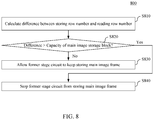
- FIG. 8 is a flow chart of a synchronization flow 800 performed during the operation of the synchronization circuit 150 in another embodiment of the present invention.
- the embodiment of the main image storage block 112 that operates as the ring buffer is further described in detail in accompany with FIG. 7 and FIG. 8 in the following paragraphs.
- the synchronization circuit 150 illustrated in FIG. 7 is similar to the synchronization circuit 150 illustrated in FIG. 4 and includes the first comparison module 400 , the second comparison module 402 and the synchronization processing module 404 .
- the synchronization circuit 150 illustrated in FIG. 7 further includes a first calculation module 406 .
- the first calculation module 406 is configured to calculate a difference DR between the storing row number RW and the reading row number RR according to the frame processing information FP 1 and FP 2 .
- the synchronization mechanism performed by the synchronization circuit 150 illustrated in FIG. 7 further includes the flow illustrated in FIG. 8 .
- Step S 810 The first calculation module 406 calculates the difference DR between the storing row number RW and the reading row number RR.
- Step S 820 The synchronization processing module 404 determines whether the difference DR exceeds the capacity of the main image storage block 112 .
- Step S 830 When the difference DR does not exceed the capacity of the main image storage block 112 , the internal effective content that is not encoded does not fully occupy the capacity of the main image storage block 112 .
- the synchronization processing module 404 allows the former stage circuit 120 to keep storing the N-th main image frame.
- Step S 840 On the contrary, when the difference DR exceeds the capacity of the main image storage block 112 , the speed that the former stage circuit 120 stores the main image frame is faster than the speed that the latter stage circuit 130 reads the main image frame. If the storing is kept being performed, the data of the main image frame that the latter stage circuit 130 has not read yet is going to be replaced. As a result, by using the former stage circuit control signal CC 2 , the synchronization processing module 404 stops the former stage circuit 120 from storing the N-th main image frame. The storing of the data of the main image frame is therefore stopped temporarily.
- the embodiment of the main image storage block 112 operating as a ring buffer not only avoids the condition that the incorrect data is read when the speed of the read operation of the latter stage circuit 130 is too fast, but also avoids the condition that the data that the latter stage circuit 130 has not read is replaced when the speed of the storage operation of the former stage circuit 120 is too fast.
- FIG. 9 is a timing diagram of the image processing performed by the multi-stream image processing apparatus 100 in another embodiment of the present invention.
- the time sequence during the processing of the multi-stream image processing apparatus 100 includes a plurality of image frame processing time periods, such as the consecutive three image frame processing time periods T N ⁇ 1 , T N and T N+1 exemplarily illustrated in FIG. 9 .
- Each two adjacent image frame processing time periods include a synchronization signal time period therebetween, such as the synchronization signal time period TS N between the image frame processing time periods T N ⁇ 1 and T N , and the synchronization signal time period TS N+1 between the image frame processing time periods T N and T N+1 .
- the synchronization signal time periods TS N and TS N+1 respectively correspond to the transmission of the synchronization signals S N and S N+1 to respectively mark the beginning of the image frame processing time periods T N and T N+1 .
- the latter stage circuit 130 still reads and processes the N ⁇ 1-th sub image frames of the sub image streams SS 1 and SS 2 .
- the latter stage circuit 130 still reads and processes the N-th main image frame.
- the image frame processing time period T N further includes a third sub period T S3 before the first sub period T S1 .
- the latter stage circuit 130 not only processes the N ⁇ 1-th main image frame in a latter part of the image frame processing time period T N ⁇ 1 , but also processes the N ⁇ 1-th main image frame in the synchronization signal time period TS N and the third sub period T S3 .
- the latter stage circuit 130 can also process the N-th main image frame in the latter part of the image frame processing time period T N , the synchronization signal time period TS N+1 and the third sub period T S3 in the image frame processing time period T N+1 .
- the N-th sub image frames of the sub image streams SS 1 and SS 2 and the N-th main image frame of the main image stream MS are still stored from the beginning of the image frame processing time period T N .
- the N ⁇ 1-th main image frame is read and the N-th main image frame is stored simultaneously in the main image storage block 112 .
- the advantage of applying the third sub period T S3 is that the latter stage circuit can perform data processing with a slower speed and accomplish a power-saving mechanism.
- FIG. 10 is a block diagram of the synchronization circuit 150 in yet another embodiment of the present invention.
- FIG. 11 is a flow chart of a synchronization flow 1100 performed during the operation of the synchronization circuit 150 in yet another embodiment of the present invention.
- the embodiment of the main image storage block 112 that operates as the ring buffer is further described in detail in accompany with FIG. 10 and FIG. 11 in the following paragraphs.
- the synchronization circuit 150 illustrated in FIG. 10 is similar to the synchronization circuit 150 illustrated in FIG. 7 and includes the first comparison module 400 , the second comparison module 402 , the synchronization processing module 404 and the first calculation module 406 .
- the synchronization circuit 150 illustrated in FIG. 10 further includes a second calculation module 408 .
- the second calculation module 408 is configured to operate when the image frame that the former stage circuit 120 currently stores and the image frame that the latter stage circuit 130 currently reads are different.
- the synchronization mechanism performed by the synchronization circuit 150 illustrated in FIG. 10 includes the flow including the steps S 510 , S 520 and S 540 to S 570 illustrated in FIG. 5 and the flow including the steps S 810 to S 840 illustrated in FIG. 8 .
- the synchronization circuit 150 illustrated in FIG. 10 operates the flow illustrated in FIG. 11 to activate the synchronization mechanism.
- Step S 1110 According to the frame processing information FP 1 and FP 2 , the second calculation module 408 calculates a difference between the size FR of the N ⁇ 1-th main image frame and the reading row number RR of the N ⁇ 1-th main image frame. Such a difference stands for the remained data amount in the N ⁇ 1-th main image frame that is not read and processed by the latter stage circuit 130 . Subsequently, the second calculation module 408 calculates a sum SUM of the difference and the storing row number RW of the N-th main image frame. The storing row number RW stands for the data amount in the N-th main image frame that the former stage circuit 120 is stored.
- Step S 1120 the synchronization processing module 404 determines whether the sum SUM exceeds the capacity of the main image storage block 112 .
- Step S 1130 When the sum SUM does not exceed the capacity of the main image storage block 112 , the speed that the former stage circuit 120 performs storage operation does not exceed the speed that the latter stage circuit 130 performs read operation. As a result, by using the former stage circuit control signal CC 2 , the synchronization processing module 404 allows the former stage circuit 120 to keep storing the N-th main image frame.
- Step S 1140 On the contrary, when the sum SUM exceeds the capacity of the main image storage block 112 , the speed that the former stage circuit 120 performs storage operation exceeds the speed that the latter stage circuit 130 performs read operation. If the storing is kept being performed, the data of the main image frame that the latter stage circuit 130 has not read yet is going to be replaced. As a result, by using the former stage circuit control signal CC 2 , the synchronization processing module 404 stops the former stage circuit 120 from storing the N-th main image frame. The storing of the data of the main image frame is therefore stopped temporarily.
- the multi-stream image processing apparatus 100 of the present invention can use a single latter stage circuit to process the plurality of image streams generated by the former stage circuit with a time-division method to avoid the cost of disposition of a plurality of latter stage circuits.
- the memory module only needs to store N ⁇ 1-th sub image frame and the N-th sub image frame corresponding to the sub image frames having a lower data amount due to the lower resolution.
- the disposition of two storage blocks is not necessary.
- the space cost of the memory module can be reduced as well.
- the memory module can include the main image storage block implemented by the ring buffer.
- the capacity can be reduced to further reduce the space cost of the memory module.
- the multi-stream image processing apparatus and the multi-stream image processing method of the present invention can reduce the hardware disposition cost of the latter stage circuit and the space cost of the memory.
Landscapes
- Engineering & Computer Science (AREA)
- Multimedia (AREA)
- Signal Processing (AREA)
- Physics & Mathematics (AREA)
- General Physics & Mathematics (AREA)
- Theoretical Computer Science (AREA)
- Two-Way Televisions, Distribution Of Moving Picture Or The Like (AREA)
- Television Systems (AREA)
- Studio Devices (AREA)
- Image Processing (AREA)
- Controls And Circuits For Display Device (AREA)
Abstract
Description
- The present disclosure relates to a multi-stream image processing technology, especially to a multi-stream image processing apparatus and method of the same.
- In some applications of the image processing technology, a plurality of image streams are generated according to the same image source. For example, after retrieving the images of the environment, an IP camera may generate a plurality of image streams, while some image streams having higher resolution can be displayed as higher resolution frames on a corresponding display module, and some image streams having lower resolution can be displayed on a display module having a lower resolution to provide an instant surveillance mechanism.
- However, a plurality of corresponding circuits are required to perform image processing on a plurality of image streams. The cost of the circuits is thus increased.
- In consideration of the problem of the prior art, an object of the present disclosure is to provide a multi-stream image processing apparatus and a multi-stream image processing method to perform process on a plurality of image streams by using a single latter stage circuit with a time-division method to avoid the high cost of disposition of a multiple of latter stage circuits.
- The present disclosure discloses a multi-stream image processing method that includes steps outlined below. A plurality of image streams are generated by a former stage circuit according to a same image source, wherein the image streams comprises a main image stream and at least one sub image stream, and a resolution of the main image stream is higher than a resolution of the sub image stream. Within an image frame processing time period, a N-th sub image frame of the sub image stream is stored by the former stage circuit in at least one current sub image storage block of a memory module and a N-th main image frame of the main image stream is stored by the former stage circuit in a main image storage block of the memory module. Within a first sub period of the image frame processing time period, a N−1-th sub image frame of the sub image stream stored in a previous sub image storage block of the memory module is read by a latter stage circuit and the N−1-th sub image frame is processed by the latter stage circuit. Within a second sub period of the image frame processing time period behind the first sub period, the N-th main image frame stored in the main image storage block is read by the latter stage circuit and the N-th main image frame is processed by the latter stage circuit.
- The present disclosure also discloses a multi-stream image processing apparatus that includes a memory module, a former stage circuit, a latter stage circuit and a processing circuit. The processing circuit is electrically coupled to the memory module, the former stage circuit and the latter stage circuit, and is configured to execute a plurality of software or firmware executable commands to execute a multi-stream image processing method. The multi-stream image processing method includes steps outlined below. A plurality of image streams are generated by the former stage circuit according to a same image source, wherein the image streams comprises a main image stream and at least one sub image stream, and a resolution of the main image stream is higher than a resolution of the sub image stream. Within an image frame processing time period, a N-th sub image frame of the sub image stream is stored by the former stage circuit in at least one current sub image storage block of a memory module and a N-th main image frame of the main image stream is stored by the former stage circuit in a main image storage block of the memory module. Within a first sub period of the image frame processing time period, a N−1-th sub image frame of the sub image stream stored in a previous sub image storage block of the memory module is read by the latter stage circuit and the N−1-th sub image frame is processed by the latter stage circuit. Within a second sub period of the image frame processing time period behind the first sub period, the N-th main image frame stored in the main image storage block is read by the latter stage circuit and the N-th main image frame is processed by the latter stage circuit.
- These and other objectives of the present disclosure will no doubt become obvious to those of ordinary skill in the art after reading the following detailed description of the preferred embodiments that are illustrated in the various figures and drawings.
-
FIG. 1 is a block diagram of a multi-stream image processing apparatus in an embodiment of the present invention. -
FIG. 2 is a flow chart of a multi-stream image processing method in an embodiment of the present invention. -
FIG. 3 is a timing diagram of the image processing performed by the multi-stream image processing apparatus in an embodiment of the present invention. -
FIG. 4 is a block diagram of the synchronization circuit in an embodiment of the present invention. -
FIG. 5 is a flow chart of a synchronization flow performed during the operation of the synchronization circuit in an embodiment of the present invention. -
FIG. 6 is a diagram of the main image frame in an embodiment of the present invention. -
FIG. 7 is a block diagram of the synchronization circuit in another embodiment of the present invention. -
FIG. 8 is a flow chart of a synchronization flow performed during the operation of the synchronization circuit in another embodiment of the present invention. -
FIG. 9 is a timing diagram of the image processing performed by the multi-stream image processing apparatus in another embodiment of the present invention. -
FIG. 10 is a block diagram of the synchronization circuit in yet another embodiment of the present invention. -
FIG. 11 is a flow chart of a synchronization flow performed during the operation of the synchronization circuit in yet another embodiment of the present invention. - An aspect of the present invention is to provide a multi-stream image processing apparatus and a multi-stream image processing method to perform process on a plurality of image streams by using a single latter stage circuit with a time-division method to avoid the high cost of disposition of a multiple of latter stage circuits.
- Reference is now made to
FIG. 1 .FIG. 1 is a block diagram of a multi-streamimage processing apparatus 100 in an embodiment of the present invention. The multi-streamimage processing apparatus 100 is able to retrieve the images of an environment to generate a plurality of image streams MS (main image stream), SS1 (first sub image stream) and SS2 (second sub image stream) according to the same image source IS and subsequently perform processing on the image streams MS, SS1 and SS2 to generate a processed main image stream EMS, a processed first sub image stream ESS1 and a processed second sub image stream ESS2. - The multi-stream
image processing apparatus 100 includes amemory module 110, aformer stage circuit 120, alatter stage circuit 130, aprocessing circuit 140 and asynchronization circuit 150. - In an embodiment, the
memory module 110 has different blocks to store different data required to process the plurality of image streams. Thememory module 110 can be implemented by a memory having a higher speed such as, but not limited to a double data rate synchronous dynamic random access memory (DDR SDRAM). - In an embodiment, the multi-stream
image processing apparatus 100 may further include amemory controller 115. Thememory controller 115 can be implemented by such as, but not limited to a memory interface unit (MIU). Other circuit modules in the multi-streamimage processing apparatus 100, e.g. theformer stage circuit 120 and thelatter stage circuit 130, can perform read operation and write operation on thememory module 110 through thememory controller 115 to store data in thememory module 110 or retrieve data from thememory module 110. - In an embodiment, the
former stage circuit 120 is an image signal processor (ISP) configured to generate the plurality of image streams MS, SS1 and SS2 according to the same image source IS. The image source IS can be such as, but not limited to image sensing components in an IP camera. After the image sensing components sense the image, theformer stage circuit 120 generates the image streams MS, SS1 and SS2 accordingly and stores the image streams MS, SS1 and SS2 having different resolutions in thememory module 110 through thememory controller 115. - The image stream MS is a main image stream and the image streams SS1 and SS2 are respectively a first sub image stream and a second sub image stream. The resolution of the main image stream MS is higher than the resolution of the first sub image stream SS1 and the resolution of the second sub image stream SS2. In an embodiment, the resolution of the main image stream MS is 4K, The resolution of the first sub image stream SS1 is 1280×720. The resolution of the second sub image stream SS2 is 720×576. It is appreciated that the number of the sub image streams and the resolution of each of the image streams described above are merely an example. The present invention is not limited thereto. In an embodiment, the number of the sub image stream can be one or more than one.
- In an embodiment, the
latter stage circuit 130 is an encoder configured to read the image streams MS, SS1 and SS2 from thememory module 110 through thememory controller 115 to perform encoding process and generate the processed main image stream EMS, the processed first sub image stream ESS1 and the processed second sub image stream ESS2 that are finished being encoded. In different embodiments, the encoding process is performed based on such as, but not limited to H264, H265 or other encoding standards. - The
synchronization circuit 150 is electrically coupled to theformer stage circuit 120, thelatter stage circuit 130 and theprocessing circuit 140 and is configured to, according to the control of theprocessing circuit 140, balance the speed that theformer stage circuit 120 stores the image stream to thememory module 110 and the speed that thelatter stage circuit 130 reads the image stream from thememory module 110. - The
processing circuit 140 is electrically coupled to thememory module 110, theformer stage circuit 120, thelatter stage circuit 130 and thesynchronization circuit 150. Theprocessing circuit 140 can execute software orfirmware executable commands 141 to perform the function of the multi-streamimage processing apparatus 100. More specifically, theprocessing circuit 140 can retrieve the software orfirmware executable commands 141 from a storage module (not illustrated) included in the multi-streamimage processing apparatus 100, in which the software orfirmware executable commands 141 include such as, but not limited to firmware of theformer stage circuit 120, thelatter stage circuit 130 and thesynchronization circuit 150 and other related commands for operating and controlling theformer stage circuit 120, thelatter stage circuit 130 and thesynchronization circuit 150. Theprocessing circuit 140 further operates and controls theformer stage circuit 120, thelatter stage circuit 130 and thesynchronization circuit 150 accordingly to perform the storing, reading and encoding of the image streams MS, SS1 and SS2 and generate the processed main image stream EMS, the processed first sub image stream ESS1 and the processed second sub image stream ESS2. - It is appreciated that in an embodiment, the storage module can be implemented by another memory independent from the
memory module 110. For example, the storage module can be implemented by such as, but not limited to a optical disk, a random access memory (RAM), a read only memory (ROM), a floppy disk, a hard drive or a CD-ROM. In another embodiment, the storage module can also be implemented together with thememory module 110 as a single memory. - Reference is now made to
FIG. 2 at the same time. The detail function of the multi-streamimage processing apparatus 100 is further described in accompany withFIG. 1 andFIG. 2 in the following paragraphs. -
FIG. 2 is a flow chart of a multi-streamimage processing method 200 in an embodiment of the present invention. The multi-streamimage processing method 200 can be used in the multi-streamimage processing apparatus 100 illustrated inFIG. 1 . In an embodiment, the multi-streamimage processing method 200 includes the steps illustrated inFIG. 2 . - Step S210: a plurality of image streams MS, SS1 and SS2 are generated by the
former stage circuit 120 according to the same image source IS. As described above, image streams MS, SS1 and SS2 include the main image stream MS, the first sub image stream SS1 and the second sub image stream SS2. The resolution of the main image stream MS is higher than the resolution of each of the first and the second sub image streams SS1 and SS2. - Step S220: Within an image frame processing time period, a N-th sub image frame of the sub image stream SS1 is stored by the
former stage circuit 120 in the current first subimage storage block 114A of thememory module 110, a N-th sub image frame of the sub image stream SS2 is stored by theformer stage circuit 120 in the current second subimage storage block 116A of thememory module 110, and a N-th main image frame of the main image stream MS is stored by theformer stage circuit 120 in a mainimage storage block 112 of thememory module 110. N is a positive integer. - Reference is now made to
FIG. 3 at the same time.FIG. 3 is a timing diagram of the image processing performed by the multi-streamimage processing apparatus 100 in an embodiment of the present invention. - The time sequence during the processing of the multi-stream
image processing apparatus 100 includes a plurality of image frame processing time periods, such as the consecutive three image frame processing time periods TN−1, TN and TN+1 exemplarily illustrated inFIG. 3 . Each two adjacent image frame processing time periods include a synchronization signal time period therebetween, such as the synchronization signal time period TSN between the image frame processing time periods TN−1 and TN, and the synchronization signal time period TSN+1 between the image frame processing time periods TN and TN+1. The synchronization signal time periods TSN and TSN+1 respectively correspond to the transmission of the synchronization signals SN and SN+1 and respectively mark the beginning of the image frame processing time periods TN and TN+1. - In the present embodiment, within the synchronization signal time periods TSN and TSN+1, both of the
former stage circuit 120 and thelatter stage circuit 130 do not perform data processing. Theformer stage circuit 120 and thelatter stage circuit 130 only perform data processing within the image frame processing time periods TN−1, TN and TN+1. - In
FIG. 3 , the time periods corresponding to the processing of theformer stage circuit 120 is illustrated as blocks having slashes. Since theformer stage circuit 120 can simultaneously generate the image streams MS, SS1 and SS2, theformer stage circuit 120 simultaneously stores the N-th sub image frame of the sub image stream SS1 in the current first subimage storage block 114A, stores the N-th sub image frame of the sub image stream SS2 in the current second subimage storage block 116A and stores the N-th main image frame of the main image stream MS in the mainimage storage block 112 after the image frame processing time period TN begins. - Step S230: Within a first sub period TS1 of the image frame processing time period TN, a N−1-th sub image frame of the sub image stream SS1 stored in a previous first sub
image storage block 114B of thememory module 110 is read by thelatter stage circuit 130 and a N−1-th sub image frame of the sub image stream SS2 stored in a previous second subimage storage block 116B of thememory module 110 is read by thelatter stage circuit 130. The N−1-th sub image frame of the sub image stream SS1 and the N−1-th sub image frame of the sub image stream SS2 are processed by thelatter stage circuit 130. - In an embodiment, as illustrated in
FIG. 3 , within the image frame processing time period TN−1, the N−1-th sub image frame of the sub image stream SS1 and the N−1-th sub image frame of the sub image stream SS2 are respectively stored in the previous first subimage storage block 114B and the previous second subimage storage block 116B by theformer stage circuit 120 through thememory controller 115. - The time periods corresponding to the processing of the
latter stage circuit 130 is illustrated as blocks having dots. Thelatter stage circuit 130 is operated by using a time-division method to process one image frame in one time period. As illustrated inFIG. 3 , within the first sub period TS1, thelatter stage circuit 130 first reads the N−1-th sub image frame corresponding to the first sub image stream SS1 from the previous first subimage storage block 114B and processes the N−1-th sub image frame to generate the image frame corresponding to the processed first sub image stream ESS1. Subsequently, within the remained time period within the first sub period TS1, thelatter stage circuit 130 reads the N−1-th sub image frame corresponding to the second sub image stream SS2 from the previous second subimage storage block 116B and processes the N−1-th sub image frame to generate the image frame corresponding to the processed second sub image stream ESS2. - Step S240: Within a second sub period TS2 of the image frame processing time period TN behind the first sub period TS1, the N-th main image frame stored in the main
image storage block 112 is read by thelatter stage circuit 130 and the N-th main image frame is processed by thelatter stage circuit 130. - In an embodiment, a capacity of the main
image storage block 112 is larger than or equals to a size of the N-th main image frame. In some embodiments, the operation speed of thelatter stage circuit 130 may be faster than the operation speed of theformer stage circuit 120. As a result, in order to avoid the occurrence of the condition that the speed that thelatter stage circuit 130 reads data from the mainimage storage block 112 exceeds the speed that theformer stage circuit 120 stores data to the mainimage storage block 112, thesynchronization circuit 150 performs coordination and synchronization between theformer stage circuit 120 and thelatter stage circuit 130. - Reference is now made to
FIG. 4 .FIG. 4 is a block diagram of thesynchronization circuit 150 in an embodiment of the present invention. - As illustrated in
FIG. 4 , thesynchronization circuit 150 includes afirst comparison module 400, asecond comparison module 402 and asynchronization processing module 404. - The
first comparison module 400 and thesecond comparison module 402 can retrieve frame processing information FP1 and FP2 from theformer stage circuit 120 and thelatter stage circuit 130 respectively. The frame processing information FP1 includes a former stage frame number F1 and a storing row number RW of the image frame that theformer stage circuit 120 currently stores. The frame processing information FP2 includes a latter stage frame number F2 and a reading row number RR of the image frame that thelatter stage circuit 130 currently reads. - In an embodiment, the
first comparison module 400 performs comparison according to the former stage frame number F1 of the image frame that theformer stage circuit 120 currently stores and the latter stage frame number F2 of the image frame that thelatter stage circuit 130 currently reads to determine whether the image frame that theformer stage circuit 120 currently stores and the image frame that thelatter stage circuit 130 currently reads are the same image frame. Thesecond comparison module 402 performs comparison according to the storing row number RW of the image frame that theformer stage circuit 120 currently stores and the reading row number RR of the image frame that thelatter stage circuit 130 currently reads to determine whether the reading row number RR of the image frame that thelatter stage circuit 130 currently reads exceeds the storing row number RW of the image frame that theformer stage circuit 120 currently stores. - The
synchronization processing module 404 further determines the operation condition of theformer stage circuit 120 and thelatter stage circuit 130 according to the comparison results of thefirst comparison module 400 and thesecond comparison module 402 to further determines the synchronization strategy being used. - Reference is now made to
FIG. 5 at the same time.FIG. 5 is a flow chart of asynchronization flow 500 performed during the operation of thesynchronization circuit 150 in an embodiment of the present invention. The operation mechanism of thesynchronization circuit 150 is further described in detail in accompany withFIG. 4 andFIG. 5 in the following paragraphs. - Step S510: As illustrated in
FIG. 5 , thefirst comparison module 400 retrieves the former stage frame number F1 and the latter stage frame number F2 in the frame processing information FP1 and the frame processing information FP2 respectively from theformer stage circuit 120 and thelatter stage circuit 130 to perform comparison. - Step S520: According to the first comparison result CR1 of the
first comparison module 400, thesynchronization processing module 404 further determines whether the image frame that theformer stage circuit 120 currently stores and the image frame that thelatter stage circuit 130 currently reads are the same image frame. - Step S530: When the image frame that the
former stage circuit 120 currently stores and the image frame that thelatter stage circuit 130 currently reads are not the same image frame, e.g. the condition within the first sub period TS1 of the image frame processing time period TN, in which thelatter stage circuit 130 reads the N−1-th sub image frame and theformer stage circuit 120 stores the N-th main image frame, thesynchronization processing module 404 does not activate the synchronization mechanism of thesynchronization circuit 150. - Step S540: When the image frame that the
former stage circuit 120 currently stores and the image frame that thelatter stage circuit 130 currently reads are the same image frame, e.g. the condition within the second sub period TS2 of the image frame processing time period TN, in which thelatter stage circuit 130 reads the N-th sub image frame and theformer stage circuit 120 also stores the N-th main image frame, thesynchronization processing module 404 activates the synchronization mechanism of thesynchronization circuit 150. Thesecond comparison module 402 retrieves the storing row number RW and the reading row number RR in the frame processing information FP1 and FP2 respectively from theformer stage circuit 120 and thelatter stage circuit 130 to perform comparison. - Reference is now made to
FIG. 6 at the same time.FIG. 6 is a diagram of themain image frame 600 in an embodiment of the present invention. - Step S550: According to the second comparison result CR2 of the
second comparison module 402, thesynchronization processing module 404 determines whether the storing row number RW of themain image frame 600 that theformer stage circuit 120 currently stores exceeds the reading row number RR of themain image frame 600 that thelatter stage circuit 130 currently reads. - Step S560: When the storing row number RW exceeds the reading row number RR, the content read by the
latter stage circuit 130 does not exceed the content stored by theformer stage circuit 120. As a result, by delivering a latter stage circuit control signal CC1, thesynchronization processing module 404 allows thelatter stage circuit 130 to keep reading the N-th main image frame and process the N-th main image frame. - Step S570: On the contrary, when the storing row number RW does not exceed the reading row number RR, the content read by the
latter stage circuit 130 exceeds the content stored by theformer stage circuit 120. As a result, by delivering the latter stage circuit control signal CC1, thesynchronization processing module 404 stops thelatter stage circuit 130 from reading the N-th main image frame to avoid the reading of the incorrect data content. - As a result, under the coordination and the synchronization of the
synchronization circuit 150, thelatter stage circuit 130 can read the content of the N-th main image frame in an order to process the N-th main image frame and generate the main image frame corresponding to the processed main image stream EMS. It is appreciated that in the present embodiment, thelatter stage circuit 130 finishes processing the N-th main image frame before the next synchronization signal time period TSN+1. - Furthermore, within the image frame processing time period TN+1, the
former stage circuit 120 can store the N+1-th sub image frames of the sub image streams SS1 and SS2 and the N+1-th main image frame of the main image stream MS by using the method described above. - Further, by using the method described above, the
latter stage circuit 130 can read and process the N-th sub image frames of the sub image streams SS1 and SS2 first and subsequently reads and processes the N+1-th main image frame of the main image stream MS. - It is appreciated that in an embodiment, the current first sub
image storage block 114A and the second subimage storage block 116A that theformer stage circuit 120 uses to store the N-th sub image frames of the sub image streams SS1 and SS2 within the image frame processing time period TN become the previous sub image storage blocks in the image frame processing time period TN+1. The previous first subimage storage block 114B and the previous second subimage storage block 116B in the image frame processing time period TN becomes current sub image storage block in the image frame processing time period TN+1 and are used to store the N+1-th sub image frames of the sub image streams SS1 and SS2. - The embodiments described above use the condition that the capacity of the main
image storage block 112 is larger than or equals to the size of the N-th main image frame as an example. In another embodiment, the capacity of the mainimage storage block 112 can be smaller than the size of the N-th main image frame and the mainimage storage block 112 operates as a ring buffer. In other words, when the part of the main image frame stored by theformer stage circuit 120 reaches the highest address of the mainimage storage block 112, the latest data of the image frame further replaces the lowest address of the mainimage storage block 112. When the part of the main image frame read by thelatter stage circuit 130 reaches the highest address of the mainimage storage block 112, the data is kept reading from the lowest address of the mainimage storage block 112. - Reference is now made to
FIG. 7 andFIG. 8 at the same time.FIG. 7 is a block diagram of thesynchronization circuit 150 in another embodiment of the present invention.FIG. 8 is a flow chart of asynchronization flow 800 performed during the operation of thesynchronization circuit 150 in another embodiment of the present invention. The embodiment of the mainimage storage block 112 that operates as the ring buffer is further described in detail in accompany withFIG. 7 andFIG. 8 in the following paragraphs. - The
synchronization circuit 150 illustrated inFIG. 7 is similar to thesynchronization circuit 150 illustrated inFIG. 4 and includes thefirst comparison module 400, thesecond comparison module 402 and thesynchronization processing module 404. In the present embodiment, thesynchronization circuit 150 illustrated inFIG. 7 further includes afirst calculation module 406. Thefirst calculation module 406 is configured to calculate a difference DR between the storing row number RW and the reading row number RR according to the frame processing information FP1 and FP2. - Besides the flow including the steps S510 to S570 illustrated in
FIG. 5 , the synchronization mechanism performed by thesynchronization circuit 150 illustrated inFIG. 7 further includes the flow illustrated inFIG. 8 . - Step S810: The
first calculation module 406 calculates the difference DR between the storing row number RW and the reading row number RR. - Step S820: The
synchronization processing module 404 determines whether the difference DR exceeds the capacity of the mainimage storage block 112. - Step S830: When the difference DR does not exceed the capacity of the main
image storage block 112, the internal effective content that is not encoded does not fully occupy the capacity of the mainimage storage block 112. As a result, by using the former stage circuit control signal CC2, thesynchronization processing module 404 allows theformer stage circuit 120 to keep storing the N-th main image frame. - Step S840: On the contrary, when the difference DR exceeds the capacity of the main
image storage block 112, the speed that theformer stage circuit 120 stores the main image frame is faster than the speed that thelatter stage circuit 130 reads the main image frame. If the storing is kept being performed, the data of the main image frame that thelatter stage circuit 130 has not read yet is going to be replaced. As a result, by using the former stage circuit control signal CC2, thesynchronization processing module 404 stops theformer stage circuit 120 from storing the N-th main image frame. The storing of the data of the main image frame is therefore stopped temporarily. - As a result, by using the mechanism described above, the embodiment of the main
image storage block 112 operating as a ring buffer not only avoids the condition that the incorrect data is read when the speed of the read operation of thelatter stage circuit 130 is too fast, but also avoids the condition that the data that thelatter stage circuit 130 has not read is replaced when the speed of the storage operation of theformer stage circuit 120 is too fast. - Reference is now made to
FIG. 9 at the same time.FIG. 9 is a timing diagram of the image processing performed by the multi-streamimage processing apparatus 100 in another embodiment of the present invention. - The time sequence during the processing of the multi-stream
image processing apparatus 100 includes a plurality of image frame processing time periods, such as the consecutive three image frame processing time periods TN−1, TN and TN+1 exemplarily illustrated inFIG. 9 . Each two adjacent image frame processing time periods include a synchronization signal time period therebetween, such as the synchronization signal time period TSN between the image frame processing time periods TN−1 and TN, and the synchronization signal time period TSN+1 between the image frame processing time periods TN and TN+1. The synchronization signal time periods TSN and TSN+1 respectively correspond to the transmission of the synchronization signals SN and SN+1 to respectively mark the beginning of the image frame processing time periods TN and TN+1. - In the present embodiment, during the first sub period TS1 in the image frame processing time period TN, the
latter stage circuit 130 still reads and processes the N−1-th sub image frames of the sub image streams SS1 and SS2. During the second sub period TS2 in the image frame processing time period TN, thelatter stage circuit 130 still reads and processes the N-th main image frame. - However, in the present embodiment, besides the feature that the main
image storage block 112 is implemented by a ring buffer, the image frame processing time period TN further includes a third sub period TS3 before the first sub period TS1. For the N−1-th main image frame that the image frame processing time period TN−1 corresponds to, thelatter stage circuit 130 not only processes the N−1-th main image frame in a latter part of the image frame processing time period TN−1 , but also processes the N−1-th main image frame in the synchronization signal time period TSN and the third sub period TS3. Identically, thelatter stage circuit 130 can also process the N-th main image frame in the latter part of the image frame processing time period TN, the synchronization signal time period TSN+1 and the third sub period TS3 in the image frame processing time period TN+1. - However, for the
former stage circuit 120, the N-th sub image frames of the sub image streams SS1 and SS2 and the N-th main image frame of the main image stream MS are still stored from the beginning of the image frame processing time period TN. As a result, within the third sub period TS3, the N−1-th main image frame is read and the N-th main image frame is stored simultaneously in the mainimage storage block 112. The advantage of applying the third sub period TS3 is that the latter stage circuit can perform data processing with a slower speed and accomplish a power-saving mechanism. - Reference is now made to
FIG. 10 andFIG. 11 at the same time.FIG. 10 is a block diagram of thesynchronization circuit 150 in yet another embodiment of the present invention.FIG. 11 is a flow chart of asynchronization flow 1100 performed during the operation of thesynchronization circuit 150 in yet another embodiment of the present invention. The embodiment of the mainimage storage block 112 that operates as the ring buffer is further described in detail in accompany withFIG. 10 andFIG. 11 in the following paragraphs. - The
synchronization circuit 150 illustrated inFIG. 10 is similar to thesynchronization circuit 150 illustrated inFIG. 7 and includes thefirst comparison module 400, thesecond comparison module 402, thesynchronization processing module 404 and thefirst calculation module 406. In the present embodiment, thesynchronization circuit 150 illustrated inFIG. 10 further includes asecond calculation module 408. Thesecond calculation module 408 is configured to operate when the image frame that theformer stage circuit 120 currently stores and the image frame that thelatter stage circuit 130 currently reads are different. - The synchronization mechanism performed by the
synchronization circuit 150 illustrated inFIG. 10 includes the flow including the steps S510, S520 and S540 to S570 illustrated inFIG. 5 and the flow including the steps S810 to S840 illustrated inFIG. 8 . However, in the present embodiment, when the image frame that theformer stage circuit 120 currently stores and the image frame that thelatter stage circuit 130 currently reads are determined to be different in the step S520 inFIG. 5 , e.g. the condition illustrated in the third sub period TS3, thesynchronization circuit 150 illustrated inFIG. 10 operates the flow illustrated inFIG. 11 to activate the synchronization mechanism. - Step S1110: According to the frame processing information FP1 and FP2, the
second calculation module 408 calculates a difference between the size FR of the N−1-th main image frame and the reading row number RR of the N−1-th main image frame. Such a difference stands for the remained data amount in the N−1-th main image frame that is not read and processed by thelatter stage circuit 130. Subsequently, thesecond calculation module 408 calculates a sum SUM of the difference and the storing row number RW of the N-th main image frame. The storing row number RW stands for the data amount in the N-th main image frame that theformer stage circuit 120 is stored. - Step S1120: the
synchronization processing module 404 determines whether the sum SUM exceeds the capacity of the mainimage storage block 112. - Step S1130: When the sum SUM does not exceed the capacity of the main
image storage block 112, the speed that theformer stage circuit 120 performs storage operation does not exceed the speed that thelatter stage circuit 130 performs read operation. As a result, by using the former stage circuit control signal CC2, thesynchronization processing module 404 allows theformer stage circuit 120 to keep storing the N-th main image frame. - Step S1140: On the contrary, when the sum SUM exceeds the capacity of the main
image storage block 112, the speed that theformer stage circuit 120 performs storage operation exceeds the speed that thelatter stage circuit 130 performs read operation. If the storing is kept being performed, the data of the main image frame that thelatter stage circuit 130 has not read yet is going to be replaced. As a result, by using the former stage circuit control signal CC2, thesynchronization processing module 404 stops theformer stage circuit 120 from storing the N-th main image frame. The storing of the data of the main image frame is therefore stopped temporarily. - As a result, the multi-stream
image processing apparatus 100 of the present invention can use a single latter stage circuit to process the plurality of image streams generated by the former stage circuit with a time-division method to avoid the cost of disposition of a plurality of latter stage circuits. - Further, by using the time-division method, the memory module only needs to store N−1-th sub image frame and the N-th sub image frame corresponding to the sub image frames having a lower data amount due to the lower resolution. For the main image frame having a higher data amount due to the higher resolution, the disposition of two storage blocks is not necessary. The space cost of the memory module can be reduced as well.
- Furthermore, by disposing the synchronization circuit, the memory module can include the main image storage block implemented by the ring buffer. The capacity can be reduced to further reduce the space cost of the memory module.
- It is appreciated that the embodiments described above are merely an example. In other embodiments, it should be appreciated that many modifications and changes may be made by those of ordinary skill in the art without departing, from the spirit of the invention.
- In summary, the multi-stream image processing apparatus and the multi-stream image processing method of the present invention can reduce the hardware disposition cost of the latter stage circuit and the space cost of the memory.
- The aforementioned descriptions represent merely the preferred embodiments of the present disclosure, without any intention to limit the scope of the present disclosure thereto. Various equivalent changes, alterations, or modifications based on the claims of present disclosure are all consequently viewed as being embraced by the scope of the present disclosure.
Claims (14)
Applications Claiming Priority (3)
| Application Number | Priority Date | Filing Date | Title |
|---|---|---|---|
| CN201811602356 | 2018-12-26 | ||
| CN201811602356.7A CN111372038B (en) | 2018-12-26 | 2018-12-26 | Multi-stream image processing device and method |
| CN201811602356.7 | 2018-12-26 |
Publications (2)
| Publication Number | Publication Date |
|---|---|
| US20200213601A1 true US20200213601A1 (en) | 2020-07-02 |
| US10771798B2 US10771798B2 (en) | 2020-09-08 |
Family
ID=68917538
Family Applications (1)
| Application Number | Title | Priority Date | Filing Date |
|---|---|---|---|
| US16/511,668 Active US10771798B2 (en) | 2018-12-26 | 2019-07-15 | Multi-stream image processing apparatus and method of the same |
Country Status (7)
| Country | Link |
|---|---|
| US (1) | US10771798B2 (en) |
| EP (1) | EP3675028B1 (en) |
| JP (1) | JP6894473B2 (en) |
| KR (1) | KR102191387B1 (en) |
| CN (1) | CN111372038B (en) |
| TW (1) | TWI691202B (en) |
| WO (1) | WO2020135407A1 (en) |
Families Citing this family (1)
| Publication number | Priority date | Publication date | Assignee | Title |
|---|---|---|---|---|
| US12513345B2 (en) | 2020-12-18 | 2025-12-30 | Fasetto, Inc. | Systems and methods for simultaneous multiple point of view video |
Citations (15)
| Publication number | Priority date | Publication date | Assignee | Title |
|---|---|---|---|---|
| US5351085A (en) * | 1993-06-16 | 1994-09-27 | Intel Corporation | Method and system for generating compressed image signals |
| US5367629A (en) * | 1992-12-18 | 1994-11-22 | Sharevision Technology, Inc. | Digital video compression system utilizing vector adaptive transform |
| US5432554A (en) * | 1993-06-16 | 1995-07-11 | Intel Corporation | Method and apparatus for decoding images using a specified data format |
| US5488570A (en) * | 1993-11-24 | 1996-01-30 | Intel Corporation | Encoding and decoding video signals using adaptive filter switching criteria |
| US20060153296A1 (en) * | 2003-09-12 | 2006-07-13 | Kevin Deng | Digital video signature apparatus and methods for use with video program identification systems |
| US20100111489A1 (en) * | 2007-04-13 | 2010-05-06 | Presler Ari M | Digital Camera System for Recording, Editing and Visualizing Images |
| US20110280300A1 (en) * | 2009-01-29 | 2011-11-17 | Dolby Laboratories Licensing Corporation | Methods and Devices for Sub-Sampling and Interleaving Multiple Images, EG Stereoscopic |
| US20120033933A1 (en) * | 2009-04-30 | 2012-02-09 | Hirotaka Suzuki | Display Control Device, Display Control Method, and Program |
| US20120057775A1 (en) * | 2010-04-09 | 2012-03-08 | Hirotaka Suzuki | Information processing device, information processing method, and program |
| US20120127367A1 (en) * | 2010-11-24 | 2012-05-24 | Ati Technologies Ulc | Method and apparatus for providing temporal image processing using multi-stream field information |
| US20130073946A1 (en) * | 2011-09-21 | 2013-03-21 | Mstar Semiconductor, Inc. | Method and apparatus for loading webpage content of webkit browser |
| US20150156469A1 (en) * | 2013-12-04 | 2015-06-04 | Dolby Laboratories Licensing Corporation | Decoding and Display of High Dynamic Range Video |
| US20180227586A1 (en) * | 2017-02-03 | 2018-08-09 | Korea Advanced Institute Of Science And Technology | Method and system for media synchronization |
| US20190045136A1 (en) * | 2016-03-03 | 2019-02-07 | Sony Corporation | Display control device, display control method, and program |
| US20200204811A1 (en) * | 2018-12-25 | 2020-06-25 | Xiamen Sigmastar Technology Ltd. | Image decryption apparatus and method of the same |
Family Cites Families (31)
| Publication number | Priority date | Publication date | Assignee | Title |
|---|---|---|---|---|
| JP2703417B2 (en) * | 1991-04-05 | 1998-01-26 | 富士通株式会社 | Receive buffer |
| JP2001103479A (en) * | 1999-09-29 | 2001-04-13 | Toshiba Corp | Video decoding device |
| JP2003259315A (en) * | 2002-02-28 | 2003-09-12 | Matsushita Electric Ind Co Ltd | Image transmission apparatus and image transmission method |
| US7907665B2 (en) * | 2003-03-14 | 2011-03-15 | Lsi Corporation | Multi-channel video compression system |
| JP4517592B2 (en) * | 2003-06-16 | 2010-08-04 | ソニー株式会社 | Image processing apparatus, image processing method, image processing program, and recording medium |
| JP2005176001A (en) * | 2003-12-12 | 2005-06-30 | Renesas Technology Corp | Semiconductor device and image processor |
| JP4225241B2 (en) * | 2004-05-13 | 2009-02-18 | ソニー株式会社 | Image display device |
| US7239355B2 (en) * | 2004-05-17 | 2007-07-03 | Mstar Semiconductor, Inc. | Method of frame synchronization when scaling video and video scaling apparatus thereof |
| JP4689440B2 (en) * | 2005-11-04 | 2011-05-25 | キヤノン株式会社 | Imaging apparatus and processing method |
| US7657668B2 (en) * | 2006-08-16 | 2010-02-02 | Qnx Software Systems (Wavemakers), Inc. | Clock synchronization of data streams |
| CN101202906A (en) * | 2006-12-11 | 2008-06-18 | 国际商业机器公司 | Method and equipment for processing video stream in digital video broadcast system |
| TWI397899B (en) | 2007-04-30 | 2013-06-01 | Mstar Semiconductor Inc | Display controller for displaying multiple windows and method for the same |
| CN101312528B (en) * | 2007-05-24 | 2010-06-23 | 晶睿通讯股份有限公司 | Method and system for real-time generation of video streams with different resolutions |
| US7870224B1 (en) * | 2007-06-08 | 2011-01-11 | Adobe Systems Incorporated | Managing online composite image content |
| JP2009111932A (en) * | 2007-10-31 | 2009-05-21 | Panasonic Corp | Video decoding device |
| US8933988B2 (en) | 2009-01-28 | 2015-01-13 | Nec Corporation | Picture transmission system and picture transmission method |
| BR112012007892B1 (en) * | 2010-08-09 | 2021-11-09 | Panasonic Corporation | IMAGE ENCODING METHOD, IMAGE DECODING METHOD, IMAGE ENCODING APPLIANCE AND IMAGE DECODING APPLIANCE |
| BR112013021410A2 (en) * | 2011-02-25 | 2016-10-25 | Photonis Netherlands B V | Real time image acquisition and display |
| US20150062353A1 (en) * | 2013-08-30 | 2015-03-05 | Microsoft Corporation | Audio video playback synchronization for encoded media |
| TWI604432B (en) * | 2014-03-18 | 2017-11-01 | 緯創資通股份有限公司 | Display and method for displaying video frames thereof |
| US20160119626A1 (en) * | 2014-10-22 | 2016-04-28 | Genetec Inc. | System to dispatch video decoding to dedicated hardware resources |
| US20160261908A1 (en) * | 2015-03-05 | 2016-09-08 | Htc Corporation | Media streaming system and control method thereof |
| US9916252B2 (en) * | 2015-05-19 | 2018-03-13 | Linear Algebra Technologies Limited | Systems and methods for addressing a cache with split-indexes |
| US9454820B1 (en) * | 2015-06-12 | 2016-09-27 | Google Inc. | Using a scene illuminating infrared emitter array in a video monitoring camera for depth determination |
| CN105282597B (en) * | 2015-10-17 | 2018-12-07 | 浙江宇视科技有限公司 | A kind of video flowing device for zooming and method |
| US9996894B2 (en) * | 2016-05-18 | 2018-06-12 | Realtek Singapore Pte Ltd | Image processing device, video subsystem and video pipeline |
| US9967465B2 (en) * | 2016-05-18 | 2018-05-08 | Realtek Singapore Pte Ltd | Image frame processing method |
| US9992467B2 (en) * | 2016-06-30 | 2018-06-05 | Apple Inc. | Parallel computer vision and image scaling architecture |
| CN106101545B (en) * | 2016-06-30 | 2019-10-15 | 维沃移动通信有限公司 | Image processing method and mobile terminal |
| CN106534857A (en) * | 2016-11-02 | 2017-03-22 | 深圳市维海德技术股份有限公司 | Code stream transmission method and camera based on USB |
| US10339421B2 (en) * | 2017-03-30 | 2019-07-02 | Toyota Motor Engineering & Manufacturing North America, Inc. | RGB-D scene labeling with multimodal recurrent neural networks |
-
2018
- 2018-12-26 CN CN201811602356.7A patent/CN111372038B/en active Active
-
2019
- 2019-01-16 TW TW108101589A patent/TWI691202B/en active
- 2019-03-08 KR KR1020190026900A patent/KR102191387B1/en active Active
- 2019-07-09 JP JP2019127682A patent/JP6894473B2/en active Active
- 2019-07-15 US US16/511,668 patent/US10771798B2/en active Active
- 2019-12-16 EP EP19216435.8A patent/EP3675028B1/en active Active
- 2019-12-24 WO PCT/CN2019/127870 patent/WO2020135407A1/en not_active Ceased
Patent Citations (15)
| Publication number | Priority date | Publication date | Assignee | Title |
|---|---|---|---|---|
| US5367629A (en) * | 1992-12-18 | 1994-11-22 | Sharevision Technology, Inc. | Digital video compression system utilizing vector adaptive transform |
| US5351085A (en) * | 1993-06-16 | 1994-09-27 | Intel Corporation | Method and system for generating compressed image signals |
| US5432554A (en) * | 1993-06-16 | 1995-07-11 | Intel Corporation | Method and apparatus for decoding images using a specified data format |
| US5488570A (en) * | 1993-11-24 | 1996-01-30 | Intel Corporation | Encoding and decoding video signals using adaptive filter switching criteria |
| US20060153296A1 (en) * | 2003-09-12 | 2006-07-13 | Kevin Deng | Digital video signature apparatus and methods for use with video program identification systems |
| US20100111489A1 (en) * | 2007-04-13 | 2010-05-06 | Presler Ari M | Digital Camera System for Recording, Editing and Visualizing Images |
| US20110280300A1 (en) * | 2009-01-29 | 2011-11-17 | Dolby Laboratories Licensing Corporation | Methods and Devices for Sub-Sampling and Interleaving Multiple Images, EG Stereoscopic |
| US20120033933A1 (en) * | 2009-04-30 | 2012-02-09 | Hirotaka Suzuki | Display Control Device, Display Control Method, and Program |
| US20120057775A1 (en) * | 2010-04-09 | 2012-03-08 | Hirotaka Suzuki | Information processing device, information processing method, and program |
| US20120127367A1 (en) * | 2010-11-24 | 2012-05-24 | Ati Technologies Ulc | Method and apparatus for providing temporal image processing using multi-stream field information |
| US20130073946A1 (en) * | 2011-09-21 | 2013-03-21 | Mstar Semiconductor, Inc. | Method and apparatus for loading webpage content of webkit browser |
| US20150156469A1 (en) * | 2013-12-04 | 2015-06-04 | Dolby Laboratories Licensing Corporation | Decoding and Display of High Dynamic Range Video |
| US20190045136A1 (en) * | 2016-03-03 | 2019-02-07 | Sony Corporation | Display control device, display control method, and program |
| US20180227586A1 (en) * | 2017-02-03 | 2018-08-09 | Korea Advanced Institute Of Science And Technology | Method and system for media synchronization |
| US20200204811A1 (en) * | 2018-12-25 | 2020-06-25 | Xiamen Sigmastar Technology Ltd. | Image decryption apparatus and method of the same |
Also Published As
| Publication number | Publication date |
|---|---|
| JP2020108136A (en) | 2020-07-09 |
| US10771798B2 (en) | 2020-09-08 |
| JP6894473B2 (en) | 2021-06-30 |
| CN111372038B (en) | 2021-06-18 |
| CN111372038A (en) | 2020-07-03 |
| EP3675028B1 (en) | 2025-07-16 |
| TWI691202B (en) | 2020-04-11 |
| EP3675028A1 (en) | 2020-07-01 |
| TW202025787A (en) | 2020-07-01 |
| WO2020135407A1 (en) | 2020-07-02 |
| KR20200080095A (en) | 2020-07-06 |
| KR102191387B1 (en) | 2020-12-15 |
Similar Documents
| Publication | Publication Date | Title |
|---|---|---|
| US9373154B2 (en) | Image processing apparatus having reduced line buffer size and associated method | |
| US8749667B2 (en) | System and method for maintaining maximum input rate while up-scaling an image vertically | |
| US9262314B2 (en) | Data transfer device | |
| US8884976B2 (en) | Image processing apparatus that enables to reduce memory capacity and memory bandwidth | |
| US11282483B2 (en) | Full-screen displays | |
| US10412320B1 (en) | Method and system for switching display from first video source to second video source | |
| US10771798B2 (en) | Multi-stream image processing apparatus and method of the same | |
| KR101615466B1 (en) | Capturing multiple video channels for video analytics and encoding | |
| US20170078600A1 (en) | Image capturing apparatus and control method for the same | |
| US9292912B2 (en) | Display apparatus and method for image output thereof | |
| US8085853B2 (en) | Video decoding and transcoding method and system | |
| US9456180B2 (en) | Image processing apparatus, communication system, and computer program | |
| JP2012123620A (en) | Data transfer device, data transfer method and semiconductor device | |
| US20040218670A1 (en) | Method and apparatus for reducing the bandwidth required for transmitting video data for display | |
| US20130278775A1 (en) | Multiple Stream Processing for Video Analytics and Encoding | |
| US20170032506A1 (en) | Image processing apparatus and control method thereof | |
| US20090092376A1 (en) | Video reproduction apparatus | |
| CN108696670A (en) | Tile reuse is carried out in imaging | |
| US20070052852A1 (en) | Motion picture display device | |
| JP4735448B2 (en) | Video signal processing device | |
| CN117061681A (en) | Image processing system and its control device, control method, and image processing method | |
| US20120212666A1 (en) | Apparatus and method for detecting flexible video cadence | |
| US20090322957A1 (en) | Image Processing Method and Related Apparatus for Calculating Target Motion Vector Used for Image Block to be Interpolated | |
| US20180160125A1 (en) | Stereoscopic image stream processor and stereoscopic image stream processing method | |
| JP2007329858A (en) | Moving image display device, moving image display method, and program |
Legal Events
| Date | Code | Title | Description |
|---|---|---|---|
| AS | Assignment |
Owner name: XIAMEN SIGMASTAR TECHNOLOGY LTD., CHINA Free format text: ASSIGNMENT OF ASSIGNORS INTEREST;ASSIGNORS:SUN, MING-YONG;WANG, HAO;REEL/FRAME:049754/0102 Effective date: 20190715 |
|
| FEPP | Fee payment procedure |
Free format text: ENTITY STATUS SET TO UNDISCOUNTED (ORIGINAL EVENT CODE: BIG.); ENTITY STATUS OF PATENT OWNER: LARGE ENTITY |
|
| STPP | Information on status: patent application and granting procedure in general |
Free format text: NON FINAL ACTION MAILED |
|
| STCF | Information on status: patent grant |
Free format text: PATENTED CASE |
|
| AS | Assignment |
Owner name: SIGMASTAR TECHNOLOGY LTD., CHINA Free format text: CHANGE OF NAME;ASSIGNOR:XIAMEN SIGMASTAR TECHNOLOGY LTD.;REEL/FRAME:057889/0055 Effective date: 20210621 |
|
| MAFP | Maintenance fee payment |
Free format text: PAYMENT OF MAINTENANCE FEE, 4TH YEAR, LARGE ENTITY (ORIGINAL EVENT CODE: M1551); ENTITY STATUS OF PATENT OWNER: LARGE ENTITY Year of fee payment: 4 |