US20150023001A1 - Backlight assembly and a display apparatus having the same - Google Patents
Backlight assembly and a display apparatus having the same Download PDFInfo
- Publication number
- US20150023001A1 US20150023001A1 US14/094,913 US201314094913A US2015023001A1 US 20150023001 A1 US20150023001 A1 US 20150023001A1 US 201314094913 A US201314094913 A US 201314094913A US 2015023001 A1 US2015023001 A1 US 2015023001A1
- Authority
- US
- United States
- Prior art keywords
- light source
- driving
- source part
- disposed
- driving part
- Prior art date
- Legal status (The legal status is an assumption and is not a legal conclusion. Google has not performed a legal analysis and makes no representation as to the accuracy of the status listed.)
- Granted
Links
- 239000000758 substrate Substances 0.000 claims description 83
- 238000000034 method Methods 0.000 claims description 5
- 230000003287 optical effect Effects 0.000 description 55
- 239000004973 liquid crystal related substance Substances 0.000 description 21
- 230000003247 decreasing effect Effects 0.000 description 17
- 238000009792 diffusion process Methods 0.000 description 4
- 239000011248 coating agent Substances 0.000 description 3
- 238000000576 coating method Methods 0.000 description 3
- 239000000463 material Substances 0.000 description 3
- 238000000149 argon plasma sintering Methods 0.000 description 1
- 230000000903 blocking effect Effects 0.000 description 1
- 210000002858 crystal cell Anatomy 0.000 description 1
- 230000005684 electric field Effects 0.000 description 1
- 239000011159 matrix material Substances 0.000 description 1
- 238000012986 modification Methods 0.000 description 1
- 230000004048 modification Effects 0.000 description 1
- 230000010287 polarization Effects 0.000 description 1
Images




Classifications
-
- G—PHYSICS
- G02—OPTICS
- G02F—OPTICAL DEVICES OR ARRANGEMENTS FOR THE CONTROL OF LIGHT BY MODIFICATION OF THE OPTICAL PROPERTIES OF THE MEDIA OF THE ELEMENTS INVOLVED THEREIN; NON-LINEAR OPTICS; FREQUENCY-CHANGING OF LIGHT; OPTICAL LOGIC ELEMENTS; OPTICAL ANALOGUE/DIGITAL CONVERTERS
- G02F1/00—Devices or arrangements for the control of the intensity, colour, phase, polarisation or direction of light arriving from an independent light source, e.g. switching, gating or modulating; Non-linear optics
- G02F1/01—Devices or arrangements for the control of the intensity, colour, phase, polarisation or direction of light arriving from an independent light source, e.g. switching, gating or modulating; Non-linear optics for the control of the intensity, phase, polarisation or colour
- G02F1/13—Devices or arrangements for the control of the intensity, colour, phase, polarisation or direction of light arriving from an independent light source, e.g. switching, gating or modulating; Non-linear optics for the control of the intensity, phase, polarisation or colour based on liquid crystals, e.g. single liquid crystal display cells
- G02F1/133—Constructional arrangements; Operation of liquid crystal cells; Circuit arrangements
- G02F1/1333—Constructional arrangements; Manufacturing methods
- G02F1/1335—Structural association of cells with optical devices, e.g. polarisers or reflectors
- G02F1/1336—Illuminating devices
- G02F1/133602—Direct backlight
-
- G—PHYSICS
- G02—OPTICS
- G02F—OPTICAL DEVICES OR ARRANGEMENTS FOR THE CONTROL OF LIGHT BY MODIFICATION OF THE OPTICAL PROPERTIES OF THE MEDIA OF THE ELEMENTS INVOLVED THEREIN; NON-LINEAR OPTICS; FREQUENCY-CHANGING OF LIGHT; OPTICAL LOGIC ELEMENTS; OPTICAL ANALOGUE/DIGITAL CONVERTERS
- G02F1/00—Devices or arrangements for the control of the intensity, colour, phase, polarisation or direction of light arriving from an independent light source, e.g. switching, gating or modulating; Non-linear optics
- G02F1/01—Devices or arrangements for the control of the intensity, colour, phase, polarisation or direction of light arriving from an independent light source, e.g. switching, gating or modulating; Non-linear optics for the control of the intensity, phase, polarisation or colour
- G02F1/13—Devices or arrangements for the control of the intensity, colour, phase, polarisation or direction of light arriving from an independent light source, e.g. switching, gating or modulating; Non-linear optics for the control of the intensity, phase, polarisation or colour based on liquid crystals, e.g. single liquid crystal display cells
- G02F1/133—Constructional arrangements; Operation of liquid crystal cells; Circuit arrangements
- G02F1/1333—Constructional arrangements; Manufacturing methods
- G02F1/1335—Structural association of cells with optical devices, e.g. polarisers or reflectors
- G02F1/1336—Illuminating devices
- G02F1/133602—Direct backlight
- G02F1/133603—Direct backlight with LEDs
-
- G—PHYSICS
- G02—OPTICS
- G02F—OPTICAL DEVICES OR ARRANGEMENTS FOR THE CONTROL OF LIGHT BY MODIFICATION OF THE OPTICAL PROPERTIES OF THE MEDIA OF THE ELEMENTS INVOLVED THEREIN; NON-LINEAR OPTICS; FREQUENCY-CHANGING OF LIGHT; OPTICAL LOGIC ELEMENTS; OPTICAL ANALOGUE/DIGITAL CONVERTERS
- G02F1/00—Devices or arrangements for the control of the intensity, colour, phase, polarisation or direction of light arriving from an independent light source, e.g. switching, gating or modulating; Non-linear optics
- G02F1/01—Devices or arrangements for the control of the intensity, colour, phase, polarisation or direction of light arriving from an independent light source, e.g. switching, gating or modulating; Non-linear optics for the control of the intensity, phase, polarisation or colour
- G02F1/13—Devices or arrangements for the control of the intensity, colour, phase, polarisation or direction of light arriving from an independent light source, e.g. switching, gating or modulating; Non-linear optics for the control of the intensity, phase, polarisation or colour based on liquid crystals, e.g. single liquid crystal display cells
- G02F1/133—Constructional arrangements; Operation of liquid crystal cells; Circuit arrangements
- G02F1/1333—Constructional arrangements; Manufacturing methods
- G02F1/1335—Structural association of cells with optical devices, e.g. polarisers or reflectors
- G02F1/1336—Illuminating devices
- G02F1/133602—Direct backlight
- G02F1/133612—Electrical details
Definitions
- the present invention relates to a backlight assembly and a display apparatus including the backlight assembly.
- the present invention relates to a backlight assembly for a liquid crystal display apparatus and a display apparatus including the backlight assembly.
- a liquid crystal display apparatus is used in a wide range of applications due to its small size, light weight and low-power-consumption, for example.
- the liquid crystal display apparatus includes two display panels provided with a liquid crystal layer disposed therebetween and applies a voltage to a molecular arrangement of liquid crystal molecules in the liquid crystal layer to change the molecular arrangement.
- the liquid crystal display apparatus displays an image by using changes of an optical property (for example, birefringence, rotary polarization, dichroism and light scattering) of a liquid crystal cell according to the changes of the molecular arrangement.
- an optical property for example, birefringence, rotary polarization, dichroism and light scattering
- the liquid crystal display apparatus includes a backlight assembly for providing light to a display panel for displaying an image.
- the backlight assembly includes a plurality of components, which contribute to the thickness of the liquid crystal display apparatus.
- An exemplary embodiment of the present invention provides a backlight assembly capable of improving assembly efficiency and decreasing whole thickness of a display apparatus.
- An exemplary embodiment of the present invention provides a display apparatus including the backlight assembly.
- a backlight assembly includes a first light source part comprising a plurality of light sources and extending in a first direction, a second light source part comprising a plurality of light sources, wherein the second light source part is spaced apart from and in parallel with the first light source part, and a driving part disposed between the first light source part and the second light source part.
- the driving part is connected to the first and second light source parts, and is configured to drive the light sources of the first and second light source parts.
- the driving part may include a driving part substrate, a transformer configured to boost an input voltage to a driving voltage for the light sources of the first and second light source parts, and a driving chip configured to process a driving signal for the light sources of the first and second light source parts.
- an opening may be formed through the driving part substrate.
- the transformer may be disposed in the opening.
- the driving chip of the driving part may be disposed on a surface of the driving part substrate.
- the transformer may be protruded from the surface of the driving part substrate by substantially the same height as the driving chip.
- the transformer may be disposed at a center of the driving part substrate.
- a reflecting layer may be formed on the transformer.
- a center of the first light source part may be connected to a first side of the driving part.
- a center of the second light source part may be connected to a second side of the driving part which is opposite to the first side.
- first and second connectors may be protruded from the center of the first light source part and the center of the second light source part, respectively.
- Third and fourth connectors may be protruded from the first side and the second side of the driving part, respectively.
- the first light source part and the second light source part may be connected to the driving part by first and second connecting parts, respectively.
- the first connecting part may include a first socket in which the first connecter of the first light source part is inserted, and a second socket in which the third connecter of the driving part is inserted.
- a display apparatus includes a backlight assembly, a reflecting element disposed on the backlight assembly, a display panel disposed on the reflecting element, and a receiving container configured to receive the backlight assembly, the reflecting element and the display panel.
- the backlight assembly includes a first light source part comprising a plurality of light sources and extending in a first direction, a second light source part comprising a plurality of light sources, wherein the second light source part is spaced apart from and in parallel with the first light source part, and a driving part disposed between the first light source part and the second light source part.
- the driving part is connected to the first and second light source parts, and is configured to drive the light sources of the first and second light source parts.
- the reflecting element may include a bottom portion and an inclined portion formed at boundaries of the bottom portion.
- the inclined portion may be slanted with respect to the bottom portion.
- a plurality of light holes which corresponds to each of the light sources of the first and second light source parts may be formed through the bottom portion.
- the driving part of the backlight assembly may include a driving part substrate, a transformer configured to boost an input voltage to a driving voltage for the light sources of the first and second light source parts, and a driving chip configured to process a driving signal for the light sources of the first and second light source parts.
- a first opening may be formed through the driving part substrate.
- the transformer may be disposed in the first opening.
- a second opening which exposes the transformer may be formed through the bottom portion of the reflecting element.
- the driving chip of the driving part may be disposed on a surface of the driving part substrate.
- the receiving container may include a bottom chassis and a top chassis combined with the bottom chassis.
- the bottom chassis may include a bottom plate in parallel with the display panel and a side wall extending from a boundary of the bottom plate and forming a receiving space.
- a first recess configured to receive the driving chip may be formed on the bottom plate.
- the display apparatus may further include a connecting part configured to connect the first or second light source part to the driving part.
- a second recess configured to partially receive the connecting part may be formed on the bottom plate of the bottom chassis.
- the driving part of the backlight assembly may be disposed between the bottom portion of the reflecting element and the bottom plate of the bottom chassis.
- the side wall of the bottom chassis may extend from the bottom plate.
- the side wall may include an inclined surface inclined with respect to the bottom plate and an outer wall extending from the inclined surface perpendicular to the bottom plate.
- the inclined portion of the reflecting element may make an angle about 20 degrees to about 30 degrees with respect to bottom portion.
- a display apparatus includes a backlight assembly, a reflecting element disposed on the backlight assembly, a display panel disposed on the reflecting element, and a receiving container configured to receive the backlight assembly, the reflecting element and the display panel.
- the backlight assembly includes a driving part disposed at a center of the display panel, a first light source part, a second light source part, a third light source part, a fourth light source part, a fifth light source part and a sixth light source part.
- the first light source part includes a plurality of light sources, extends in a first direction, and is connected to the driving part.
- the second light source part includes a plurality of light sources, extends in the first direction, is connected to the driving part, and disposed in a symmetrical relationship with the first light source part with respect to the driving part.
- the third light source part includes a plurality of light sources, extends in the first direction, is connected to the driving part, and is spaced apart from and disposed in parallel with the first light source part.
- the fourth light source part includes a plurality of light sources, extends in the first direction, is connected to the driving part, and is disposed in a symmetrical relationship with the third light source part with respect to the driving part.
- the fifth light source part includes a plurality of light sources, extends in the first direction, is connected to the driving part, and is spaced apart from and disposed in parallel with the third light source part.
- the sixth light source part includes a plurality of light sources, extends in the first direction, is connected to the driving part, and is disposed in a symmetrical relationship with the fifth light source part with respect to the driving part.
- one of the light sources of the first light source part and one of the light sources of the fifth light source part may be arranged in a first column. Another one of the light sources of the first light source part and another one of the light sources of the fifth light source part may be arranged in a second column. One of the light sources of the third light source part may be disposed between the first and second columns.
- a backlight assembly includes: a first light source part including a plurality of light sources arranged in a first direction; a second light source part including a plurality of light sources arranged in the first direction; and a driving part disposed between a central portion of the first and second light source parts, wherein the driving part includes an opening in which a transformer is disposed.
- FIG. 1 is an exploded perspective view illustrating a display apparatus according to an exemplary embodiment of the present invention
- FIG. 2 is a plan view illustrating a backlight assembly of FIG. 1 , according to an exemplary embodiment of the present invention
- FIG. 3 is a cross-sectional view taken along a line I-I′ of FIG. 1 ;
- FIG. 4 is a partially-enlarged cross-sectional view illustrating an inclined portion of a reflecting element and an inclined surface of a side wall of a bottom chassis, according to an exemplary embodiment of the present invention
- FIG. 5 is an exploded perspective view illustrating a connecting part of the backlight assembly of FIG. 2 , according to an exemplary embodiment of the present invention
- FIG. 6 is a plan view illustrating a backlight assembly according to an exemplary embodiment of the present invention.
- FIG. 7 is a cross-sectional view illustrating a display apparatus according to an exemplary embodiment of the present invention.
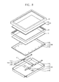
- FIG. 8 is an exploded perspective view illustrating a display apparatus according to an exemplary embodiment of the present invention.
- FIG. 9 is a cross-sectional view taken along a line II-II′ of FIG. 8 ;
- FIG. 10 is a cross-sectional view illustrating a display apparatus according to an exemplary embodiment of the present invention.
- FIG. 11 is a plan view illustrating a backlight assembly according to an exemplary embodiment of the present invention.
- FIG. 12 is a plan view illustrating a backlight assembly according to an exemplary embodiment of the present invention.
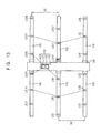
- FIG. 13 is a plan view illustrating a backlight assembly according to an exemplary embodiment of the present invention.
- FIG. 1 is an exploded perspective view illustrating a display apparatus according to an exemplary embodiment of the present invention.
- a display apparatus includes a backlight assembly 100 , a receiving container having a bottom chassis 200 and a top chassis 40 , a reflecting element 300 , an optical element 10 , a mold frame 20 and a display panel 30 .
- the backlight assembly 100 provides light to the display panel 30 .
- the backlight assembly 100 includes a driving part 110 , a first light source part 120 and a second light source part 130 .
- Each of the first light source part 120 and the second light source part 130 includes a plurality of light sources for generating the light.
- the light source may be a spot light source such as a light emitting diode (LED).
- the driving part 110 is electrically connected to the first light source part 120 and the second light source part 130 .
- the driving part 110 includes a driving circuit to drive the first light source part 120 and the second light source part 130 .
- the driving part 110 may include a transformer (refer to 112 of FIG. 2 ) for boosting an input voltage to a driving voltage for the first and second light source parts 120 and 130 , and a driving chip (refer to 114 of FIG. 2 ) for processing a driving signal for the first and second light source parts 120 and 130 .
- the reflecting element 300 is disposed on the backlight assembly 100 .
- the reflecting element 300 reflects the light from the backlight assembly 100 toward the display panel 30 .
- the reflecting element 300 includes a bottom portion 310 and an inclined portion 320 formed at boundaries of the bottom portion 310 .
- the inclined portion 320 is slanted with respect to the bottom portion 310 by a predetermined angle, so that the light from the backlight assembly 100 may be efficiently reflected toward the display panel 30 .
- a plurality of light source holes 312 which corresponds to each of the light sources of the backlight assembly 100 is formed through the bottom portion 310 .
- the reflecting element 300 is disposed on the backlight assembly 100 , the light sources of the backlight assembly 100 are exposed through the light source holes 312 .
- an opening 314 which exposes a circuit component of the driving part 110 may be formed through the bottom portion 310 .
- the transformer (refer to 112 of FIG. 2 ) of the driving part 110 may be exposed through the opening 314 .
- the optical element 10 is disposed on the reflecting element 300 .
- the optical element 10 may improve an optical property of the light from the backlight assembly 100 .
- the optical element 10 may make the light uniformly bright.
- the optical element 10 may include plurality of optical sheets.
- the optical element 10 may include a protecting sheet, a prism sheet and a diffusion sheet.
- the diffusion sheet is disposed on a light exiting surface of a light guiding plate.
- the prism sheet is disposed on the diffusion sheet.
- the protecting sheet is disposed on the prism sheet.
- the prism sheet may include an upper prism sheet and a lower prism sheet. An axis of the upper prism sheet may be substantially perpendicular to an axis of the lower prism sheet.
- the display panel 30 is disposed on the optical element 10 .
- the display panel 30 displays an image using the light from the backlight assembly 100 according to a driving signal and a data signal.
- the display panel 30 includes an array substrate 32 , an opposite substrate 34 and a liquid crystal layer (not shown) between the array substrate 32 and the opposite substrate 34 .
- the array substrate 32 includes a plurality of gate lines, a plurality of data lines crossing the gate lines, and a plurality of switching elements connected to the gate and data lines.
- the opposite substrate 34 may include a black matrix for blocking light and a color filter having a color. Although the opposite substrate 34 includes the color filter in the present exemplary embodiment, the color filter may be formed in the array substrate 32 .
- the liquid crystal layer is disposed between the array substrate 32 and the opposite substrate 34 .
- the liquid crystal layer includes liquid crystal molecules being optically anisotropic. The liquid crystal molecules are driven by an electric field, so that light may pass through or be blocked by the liquid crystal layer to display an image.
- the display panel 30 may be electrically connected to a driving part (not shown) to drive the display panel 30 .
- the driving part may be a flexible printed circuit board
- the array substrate 32 may be electrically connected to the driving part
- the driving part is disposed on a bottom or side of the backlight assembly 100 .
- the mold frame 20 supports and fixes components of the display apparatus.
- the mold frame 20 supports the display panel 30 to fix the display panel 30 in the display apparatus.
- the receiving container receives the components of the display apparatus.
- the receiving container includes the bottom chassis 200 and the top chassis 40 .
- the bottom chassis 200 includes a bottom plate 210 and a side wall 220 extending from a boundary of the bottom plate 210 .
- the bottom plate 210 and the side wall 220 form a receiving space.
- a first recess 212 and a second recess 214 are formed on the bottom plate 210 .
- the first and second recesses 212 and 214 partially receive the backlight assembly 100 .
- the backlight assembly 100 , the reflecting element 300 , the optical element 10 the mold frame 20 and the display panel 30 are received in the receiving space.
- the top chassis 40 is combined with the bottom chassis 200 .
- FIG. 2 is a plan view illustrating a backlight assembly of FIG. 1 , according to an exemplary embodiment of the present invention.
- a backlight assembly includes a driving part 110 , a first light source part 120 , a second light source part 130 and a connecting part 105 .
- the first light source part 120 has a bar shape extended in one direction.
- the first light source part 120 includes a plurality of light sources LS arranged in the direction.
- the light sources LS may be disposed at a predetermined distance from one another.
- the light source LS may be a spot light source.
- the light source LS may be an LED light source having a lens.
- the second light source part 130 is spaced apart from the first light source part 120 , and in parallel with the first light source part 120 .
- the second light source part 130 has a bar shape extended in one direction.
- the second light source part 130 includes a plurality of light sources LS arranged in the direction.
- the light sources LS may be disposed at a predetermined distance from one another.
- the light source LS may be a spot light source.
- the light source LS may be an LED light source having a lens.
- the driving part 110 is electrically connected to the first light source part 120 and the second light source part 130 , and configured to drive the first light source part 120 and the second light source part 130 .
- the driving part 110 is extended perpendicular to the direction in which the first light source part 120 and the second light source part 130 are extended.
- the first light source part 120 and the second light source part 130 may be connected by the driving part 110 at both ends of the driving part 110 .
- the driving part 110 includes a driving part substrate 115 , a transformer 112 and a driving chip 114 .
- the transformer 112 boosts an input voltage to a driving voltage for the light source LS.
- the transformer 112 may boost about 24V of the input voltage to about 300V of the driving voltage to drive the light source which is an LED light source.
- the driving chip 114 processes a driving signal for the light source LS.
- the driving chip 114 may be an integrated circuit (IC) chip for processing the driving signal for the light source LS.
- the driving chip 114 may be disposed on a rear surface of the driving part substrate 115 . Thus, the driving chip 114 may face the bottom plate 210 of the bottom chassis 200 .
- the transformer 112 may be disposed in an opening 111 formed through the driving part substrate 115 .
- the transformer 112 may be connected to a driving circuit of the driving part 110 by a connecting terminal 113 .
- the transformer 112 is disposed in the opening 111 , so that a total height of the driving part 110 may be decreased, since the transformer 112 is not disposed on the driving part substrate 115 .
- the connecting part 105 connects the first light source part 120 to the driving part 110 , and connects the second light source part 130 to the driving part 110 .
- the connecting part 105 may have a connector for connecting the first or second light source part 120 or 130 to the driving part 110 for assembly efficiency.
- the connecting part 105 is connected to a central portion of the first light source part 120 , and connected to a central portion of the second light source part 130 , so that the driving part 110 may be disposed at center the first light source part 120 and the second light source part 130 .
- the backlight assembly 100 may be driven without an additional connecting circuit board for connecting the first light source part 120 and the second light source part 130 .
- connecting part 105 A detailed explanation about the connecting part 105 will be provided in reference to FIG. 5 .
- FIG. 3 is a cross-sectional view taken along a line I-I′ of FIG. 1 .
- a display apparatus includes a backlight assembly 100 having a driving part 110 , a first light source part 120 and a second light source part 130 , a bottom chassis 200 , a reflecting element 300 , an optical element 10 , a mold frame 20 , a display panel 30 , and top chassis 40 .
- the bottom chassis 200 includes a bottom plate 210 and a side wall 220 .
- a first recess 212 and a second recess 214 are formed on the bottom plate 210 .
- the first and second recesses 212 and 214 partially receive the backlight assembly 100 .
- the side wall 220 includes an inclined surface 222 , an outside wall 224 and a supporting portion 226 .
- the inclined surface 222 extends from a boundary of the bottom plate 210 , and is inclined with respect to the bottom plate 210 .
- the outside wall 224 extends from the inclined surface 222 perpendicular to the bottom plate 210 .
- the supporting portion 226 extends from the outside wall 224 in parallel with the bottom plate 210 and is configured to support the mold frame 20 .
- the driving part 110 includes a driving part substrate 115 , a transformer 112 and a driving chip 114 .
- the driving part substrate 115 is disposed on the bottom plate 210 of the bottom chassis 200 .
- the driving chip 114 is disposed on a rear surface of the driving part substrate 115 .
- the driving chip 114 is disposed in the first recess 212 of the bottom plate 210 .
- a depth of the first recess 212 may be larger than a second height H2 of the driving chip 114 .
- the driving chip 114 may be spaced apart from a surface of the first recess 212 .
- the transformer 112 may be disposed in an opening 111 formed through the driving part substrate 115 .
- the transformer 112 may have a first height H1.
- the transformer 112 may boost about 24V of the input voltage to about 300V of the driving voltage to drive the light source which is an LED light source.
- the first height H1 of the transformer 112 may be about 15 mm.
- a length of a surface of the transformer 112 which is in parallel with the driving part substrate 115 may be about 30 mm.
- the transformer 112 may be connected to a driving circuit of the driving part 110 by a connecting terminal 113 .
- a reflecting layer 102 may be formed on the transformer 112 .
- the reflecting layer 102 may be formed by coating a reflective material on the transformer 112 .
- the first light source part 120 having the light source LS may be disposed on the bottom plate 210 of the bottom chassis 200 , and in a plane the same as the driving part 110 .
- the first light source part 120 is electrically connected by the connecting part 105 .
- the connecting part 105 is partially disposed in the second recess 214 of the bottom plate 210 of the bottom chassis 200 .
- the reflecting element 300 is disposed on the backlight assembly 100 .
- the reflecting element 300 includes a bottom portion 310 and an inclined portion 320 formed at boundaries of the bottom portion 310 .
- the inclined portion 320 is slanted with respect to the bottom portion 310 by a predetermined angle.
- the inclined portion 320 is disposed on the inclined surface 222 of the side wall 220 of the bottom chassis 200 .
- the inclined portion 320 is disposed adjacent to the light source LS, and extends to a boundary of the display apparatus.
- the number of the light sources LS of the backlight assembly 100 is decreased, and a size of the inclined portion 320 is increased, so that the angle between the inclined portion 320 and the bottom portion 310 is decreased.
- a total thickness of the display apparatus is decreased, so that the angle between the inclined portion 320 and the bottom portion 310 is decreased.
- a plurality of light source holes 312 which corresponds to each of the light sources LS is formed through the bottom portion 310 .
- the light source LS is exposed through the light source hole 312 .
- an opening 314 corresponding to the transformer 112 of the driving part 110 is formed through the bottom portion 310 .
- the transformer 112 is exposed through the opening 314 .
- the optical element 10 is disposed on the reflecting element 300 .
- the optical element 10 is spaced apart from the bottom portion 310 of the reflecting element 300 .
- the optical element 10 may improve an optical property of the light from the backlight assembly 100 .
- the mold frame 20 is disposed between the outer wall 224 of the side wall 220 of the bottom chassis 200 and the top chassis 40 .
- the mold frame 20 includes a base frame 22 , an optical element receiving portion 24 and a panel supporting part 26 .
- the base frame 22 composes a body of the mold frame 20 .
- the optical element receiving portion 24 forms a space for receiving boundaries of the optical element 10 and boundaries of the inclined portion 320 of the reflecting element 300 .
- the panel supporting part 26 supports the display panel 30 .
- the display panel 30 is disposed on the optical element 10 .
- the display panel 30 may be spaced apart from the optical element 10 by the panel supporting part 26 of the mold frame 20 .
- the display panel 30 displays an image using light from the backlight assembly 100 according to a driving signal and a data signal.
- the display panel 30 includes an array substrate 32 , an opposite substrate 34 and a liquid crystal layer (not shown) between the array substrate 32 and the opposite substrate 34 .
- the top chassis 40 is combined with the mold frame 20 and the bottom chassis 200 to fix the display panel 30 .
- FIG. 4 is a partially-enlarged cross-sectional view illustrating an inclined portion of a reflecting element and an inclined surface of a side wall of a bottom chassis, according to an exemplary embodiment of the present invention.
- the bottom chassis includes a bottom plate 210 and a side wall including an inclined surface 222 .
- the reflecting element includes a bottom portion 310 and an inclined portion 320 .
- the bottom portion 310 of the reflecting element makes a first angle a1 with the inclined portion 320 .
- the inclined portion 320 is adjacent to a light source LS of a first light source part 120 , and extends to a boundary of the display apparatus.
- the number of the light sources LS of the backlight assembly is decreased, the light source LS is disposed further from the boundary of the display apparatus and a size of the inclined portion 320 is increased, so that the first angle a1 is decreased.
- a total thickness of the display apparatus is decreased, a third height H3 of the side wall of the bottom chassis is decreased and the first angle a1 is decreased.
- the inclined surface 222 of the bottom chassis makes a second angle a2 with the bottom plate 210 .
- the second angle a2 may be the same as or larger than the first angle a1.
- the inclined surface 222 of the bottom chassis is spaced apart from the inclined portion 320 of the reflecting element in the present exemplary embodiment, the inclined portion 320 may make contact with the inclined surface 222 .
- the first angle a1 of the inclined portion 320 of the reflecting element may decrease, as the number of the light sources LS of the backlight assembly is decreased, or as the third height H3 of the side wall is decreased.
- the first angle a1 may be about 20 degrees to about 30 degrees.
- the third height H3 may be less than about 20 mm.
- FIG. 5 is an exploded perspective view illustrating a connecting part of the backlight assembly of FIG. 2 , according to an exemplary embodiment of the present invention.
- a connecting part 105 includes a first socket 105 a and a second socket 105 b opposite to the first socket 105 a.
- a connector 115 c of the driving part substrate 115 protruded from the driving part substrate 115 is inserted into the first socket 105 a of the connecting part 105 .
- a circuit pattern P is formed on the connector 115 c and electrically connected to the first socket 105 a .
- a connector 120 c of the first light source part 120 protruded from the first light source part 120 is inserted into the second socket 105 b of the connecting part 105 .
- a circuit pattern P is formed on the connector 120 c and electrically connected to the second socket 105 b .
- the first and second sockets 105 a and 105 b are electrically connected each other, so that the driving part substrate 115 and the first light source part 120 may be electrically connected to the connecting part 105 .
- FIG. 6 is a plan view illustrating a backlight assembly according to an exemplary embodiment of the present invention.
- a backlight assembly includes a driving part 110 , a first light source part 120 and a second light source part 130 .
- the first light source part 120 has a bar shape extended in one direction.
- the first light source part 120 includes first to fourth light sources LS1, LS2, LS3 and LS4 sequentially arranged in the direction.
- Each of the first to fourth light sources LS1, LS2, LS3 and LS4 is spaced apart from an adjacent light source by a first distance D1.
- the second light source part 130 is spaced apart from the first light source part 120 by a second distance D2, and in parallel with the first light source part 120 .
- the second light source part 130 has a bar shape extended in one direction.
- the second light source part 130 includes fifth to eighth light sources LS5, LS6, LS7 and LS8 sequentially arranged in the direction. Each of the fifth to eighth light sources LS5, LS6, LS7 and LS8 is spaced apart from an adjacent light source by a first distance D1.
- the first distance D1 may be substantially the same as the second distance D2.
- the first to eighth light sources LS1 to LS8 may be uniformly arranged.
- the driving part 110 includes a driving part substrate 115 and a transformer 112 .
- the transformer 112 is disposed in an opening 111 formed through the driving part substrate 115 .
- the transformer 112 may be the tallest and largest component among circuit components of a driving circuit of the driving part 110 . Thus, a portion of the transformer 112 may be protruded from an opening in a reflecting element (refer to 314 and 300 of FIG. 1 ).
- the transformer 112 may be disposed at a position which is farthest from adjacent light sources (e.g., the second, third, sixth and seventh light sources LS2, LS3, LS6 and LS7) to minimize its influence on the adjacent light sources.
- the transformer 112 may be disposed at an intersection point of a first straight line and a second straight line. The first straight line is from the second light source LS2 to the seventh light source LS7. The second straight line is from the third light source LS3 to the sixth light source LS6.
- the transformer 112 may be disposed at a center of the driving part 110 .
- FIG. 7 is a cross-sectional view illustrating a display apparatus according to an exemplary embodiment of the present invention.
- a display apparatus includes a backlight assembly 100 having a driving part 110 , a first light source part 120 and a second light source part 130 , a bottom chassis 200 , a reflecting element 300 , an optical element 10 , a mold frame 20 , a display panel 30 , and top chassis 40 .
- the bottom chassis 200 includes a bottom plate 210 and a side wall 220 .
- a first recess 212 and a second recess 214 are formed on the bottom plate 210 .
- the first and second recesses 212 and 214 partially receive the backlight assembly 100 .
- the side wall 220 includes an inclined surface 222 , an outside wall 224 and a supporting portion 226 .
- the inclined surface 222 extends from a boundary of the bottom plate 210 , and is inclined with respect to the bottom plate 210 .
- the outside wall 224 extends from the inclined surface 222 perpendicular to the bottom plate 210 .
- the supporting portion 226 extends from the outside wall 224 in parallel with the bottom plate 210 and is configured to support the mold frame 20 .
- the driving part 110 includes a driving part substrate 115 , a transformer 112 and a driving chip 114 .
- the driving part substrate 115 is disposed on the bottom plate 210 of the bottom chassis 200 .
- the driving chip 114 is disposed on a rear surface of the driving part substrate 115 .
- the driving chip 114 is disposed in the first recess 212 of the bottom plate 210 .
- a depth of the first recess 212 may be larger than a second height H2 of the driving chip 114 .
- the driving chip 114 may be spaced apart from a surface of the first recess 212 .
- the transformer 112 may be disposed in an opening 111 formed through the driving part substrate 115 .
- the transformer 112 may have a first height H1.
- a portion of the transformer 112 is protruded from the rear surface of the driving part substrate 115 by a second height H2, the rest of the transformer 112 is protruded from the front surface of the driving part substrate 115 , except for the part of the transformer 112 disposed between the front and rear surfaces of the driving part substrate 115 .
- the transformer 112 is protruded from the rear surface of the driving part substrate 115 by the second height H2 the same as that of the driving chip 114 , and protruded through an opening of the reflecting element 300 .
- the depth of the first recess 212 may be minimized, and the protruded height of the transformer 112 from the reflecting element 300 may be minimized at the same time.
- the transformer 112 may be connected to a driving circuit of the driving part 110 by a connecting terminal 113 .
- a reflecting layer 102 may be formed on the transformer 112 .
- the reflecting layer 102 may be formed by coating a reflective material on the transformer 112 .
- the first light source part 120 having the light source LS may be disposed on the bottom plate 210 of the bottom chassis 200 , and in a plane the same as the driving part 110 .
- the first light source part 120 is electrically connected by the connecting part 105 .
- the connecting part 105 is partially disposed in the second recess 214 of the bottom plate 210 of the bottom chassis 200 .
- the reflecting element 300 is disposed on the backlight assembly 100 .
- the reflecting element 300 includes a bottom portion 310 and an inclined portion 320 formed at boundaries of the bottom portion 310 .
- the inclined portion 320 is slanted with respect to the bottom portion 310 by a predetermined angle.
- the inclined portion 320 is disposed on the inclined surface 222 of the side wall 220 of the bottom chassis 200 .
- the inclined portion 320 is disposed adjacent to the light source LS, and extends to a boundary of the display apparatus.
- a plurality of light source holes 312 which corresponds to each of the light sources LS is formed through the bottom portion 310 .
- the light source LS is exposed through the light source hole 312 .
- an opening 314 corresponding to the transformer 112 of the driving part 110 is formed through the bottom portion 310 .
- the transformer 112 is exposed through the opening 314 .
- the optical element 10 is disposed on the reflecting element 300 .
- the optical element 10 is spaced apart from the bottom portion 310 of the reflecting element 300 .
- the optical element 10 may improve an optical property of the light from the backlight assembly 100 .
- the mold frame 20 is disposed between the outside wall 224 of the side wall 220 of the bottom chassis 200 and the top chassis 40 .
- the mold frame 20 includes a base frame 22 , an optical element receiving portion 24 and a panel supporting part 26 .
- the base frame 22 composes a body of the mold frame 20 .
- the optical element receiving portion 24 forms a space for receiving boundaries of the optical element 10 and boundaries of the inclined portion 320 of the reflecting element 300 .
- the panel supporting part 26 supports the display panel 30 .
- the display panel 30 is disposed on the optical element 10 .
- the display panel 30 may be spaced apart from the optical element 10 by the panel supporting part 26 of the mold frame 20 .
- the display panel 30 displays an image using light from the backlight assembly 100 according to a driving signal and a data signal.
- the display panel 30 includes an array substrate 32 , an opposite substrate 34 and a liquid crystal layer (not shown) between the array substrate 32 and the opposite substrate 34 .
- the top chassis 40 is combined with the mold frame 20 and the bottom chassis 200 to fix the display panel 30 .
- FIG. 8 is an exploded perspective view illustrating a display apparatus according to an exemplary embodiment of the present invention.
- a backlight assembly illustrated therein is substantially the same as a backlight assembly of FIG. 1 except for a driving part 110 , a first recess 212 of a bottom plate 210 of a bottom chassis 200 , and a reflecting element 300 .
- a driving part 110 a driving part 110 , a first recess 212 of a bottom plate 210 of a bottom chassis 200 , and a reflecting element 300 .
- the display apparatus includes a backlight assembly 100 , a receiving container having a bottom chassis 200 and a top chassis 40 , a reflecting element 300 , an optical element 10 , a mold frame 20 and a display panel 30 .
- the backlight assembly 100 provides light to the display panel 30 .
- the backlight assembly 100 includes a driving part 110 , a first light source part 120 and a second light source part 130 .
- Each of the first light source part 120 and the second light source part 130 includes a plurality of light sources for generating the light.
- the driving part 110 is electrically connected to the first light source part 120 and the second light source part 130 .
- the driving part 110 includes a driving circuit to drive the first light source part 120 and the second light source part 130 .
- the reflecting element 300 is disposed on the backlight assembly 100 .
- the reflecting element 300 reflects the light from the backlight assembly 100 toward the display panel 30 .
- the reflecting element 300 includes a bottom portion 310 and an inclined portion 320 formed at boundaries of the bottom portion 310 .
- a plurality of light source holes 312 which corresponds to each of the light sources of the backlight assembly 100 is formed through the bottom portion 310 .
- the reflecting element 300 is disposed on the backlight assembly 100 , the light sources of the backlight assembly 100 are exposed through the light source holes 312 .
- the optical element 10 is disposed on the reflecting element 300 .
- the optical element 10 may improve an optical property of the light from the backlight assembly 100 .
- the display panel 30 is disposed on the optical element 10 .
- the display panel 30 displays an image using light from the backlight assembly 100 according to a driving signal and a data signal.
- the display panel 30 includes an array substrate 32 , an opposite substrate 34 and a liquid crystal layer (not shown) between the array substrate 32 and the opposite substrate 34 .
- the mold frame 20 supports and fixes components of the display apparatus.
- the receiving container receives the components of the display apparatus.
- the receiving container includes the bottom chassis 200 and the top chassis 40 .
- the bottom chassis 200 includes a bottom plate 210 and a side wall 220 extending from a boundary of the bottom plate 210 .
- the bottom plate 210 and the side wall 220 form a receiving space.
- a first recess 212 and a second recess 214 for receiving a portion of the backlight assembly 100 may be formed on the bottom plate 210 .
- the top chassis 40 is combined with the bottom chassis 200 .
- FIG. 9 is a cross-sectional view taken along a line II-II′ of FIG. 8 .
- a display apparatus illustrated therein is substantially the same as a display apparatus of FIG. 3 , except for a transformer 112 of a driving part 110 of a backlight assembly 100 , a first recess 212 of a bottom plate 210 of a bottom chassis 200 , and a reflecting element 300 .
- a transformer 112 of a driving part 110 of a backlight assembly 100 a transformer 112 of a driving part 110 of a backlight assembly 100
- a first recess 212 of a bottom plate 210 of a bottom chassis 200 a reflecting element 300 .
- the display apparatus includes a backlight assembly 100 having a driving part 110 , a first light source part 120 and a second light source part 130 , a bottom chassis 200 , a reflecting element 300 , an optical element 10 , a mold frame 20 , a display panel 30 , and top chassis 40 .
- the bottom chassis 200 includes a bottom plate 210 and a side wall 220 .
- a first recess 212 and a second recess 214 are formed on the bottom plate 210 .
- the first and second recesses 212 and 214 partially receive the backlight assembly 100 .
- the side wall 220 includes an inclined surface 222 , an outside wall 224 and a supporting portion 226 .
- the driving part 110 includes a driving part substrate 115 , a transformer 112 and a driving chip 114 .
- the driving part substrate 115 is disposed on the bottom plate 210 of the bottom chassis 200 .
- the driving chip 114 is disposed on a rear surface of the driving part substrate 115 .
- the driving chip 114 is disposed in the first recess 212 of the bottom plate 210 .
- a depth of the first recess 212 may be larger than a second height H2 of the driving chip 114 .
- the driving chip 114 may be spaced apart from a surface of the first recess 212 .
- the transformer 112 may be disposed on the rear surface of the driving part substrate 115 .
- the transformer 112 may have a first height H1.
- the transformer 112 may be spaced apart from the surface of the first recess 212 .
- the first height H1 of the transformer 112 is larger than the second height H2 of the driving chip 114 , so that a depth of the first recess 212 is greater than the first height H1.
- the first light source part 120 having the light source LS may be disposed on the bottom plate 210 of the bottom chassis 200 , and in a plane the same as the driving part 110 .
- the first light source part 120 is electrically connected by the connecting part 105 .
- the connecting part 105 is partially disposed in the second recess 214 of the bottom plate 210 of the bottom chassis 200 .
- the reflecting element 300 is disposed on the backlight assembly 100 .
- the reflecting element 300 includes a bottom portion 310 and an inclined portion 320 formed at boundaries of the bottom portion 310 .
- the inclined portion 320 is slanted with respect to the bottom portion 310 by a predetermined angle.
- the inclined portion 320 is disposed on the inclined surface 222 of the side wall 220 of the bottom chassis 200 .
- the inclined portion 320 is disposed adjacent to the light source LS, and extends to a boundary of the display apparatus.
- a plurality of light source holes 312 which corresponds to each of the light sources LS is formed through the bottom portion 310 .
- the light source LS is exposed through the light source hole 312 .
- the optical element 10 is disposed on the reflecting element 300 .
- the optical element 10 is spaced apart from the bottom portion 310 of the reflecting element 300 .
- the optical element 10 may improve an optical property of the light from the backlight assembly 100 .
- the mold frame 20 is disposed between the outer wall 224 of the side wall 220 of the bottom chassis 200 and the top chassis 40 .
- the mold frame 20 includes a base frame 22 , an optical element receiving portion 24 and a panel supporting part 26 .
- the display panel 30 is disposed on the optical element 10 .
- the display panel 30 may be spaced apart from the optical element 10 by the panel supporting part 26 of the mold frame 20 .
- the display panel 30 displays an image using light from the backlight assembly 100 according to a driving signal and a data signal.
- the display panel 30 includes an array substrate 32 , an opposite substrate 34 and a liquid crystal layer (not shown) between the array substrate 32 and the opposite substrate 34 .
- the top chassis 40 is combined with the mold frame 20 and the bottom chassis 200 to fix the display panel 30 .
- FIG. 10 is a cross-sectional view illustrating a display apparatus according to an exemplary embodiment of the present invention.
- a display apparatus illustrated therein is substantially the same as a display apparatus of FIG. 3 , except for a transformer 112 of a driving part 110 of a backlight assembly 100 .
- a transformer 112 of a driving part 110 of a backlight assembly 100 any further descriptions concerning the same elements will be brief or omitted.
- the display apparatus includes a backlight assembly 100 having a driving part 110 , a first light source part 120 and a second light source part 130 , a bottom chassis 200 , a reflecting element 300 , an optical element 10 , a mold frame 20 , a display panel 30 , and top chassis 40 .
- the bottom chassis 200 includes a bottom plate 210 and a side wall 220 .
- a first recess 212 and a second recess 214 are formed on the bottom plate 210 .
- the first and second recesses 212 and 214 partially receive the backlight assembly 100 .
- the side wall 220 includes an inclined surface 222 , an outside wall 224 and a supporting portion 226 .
- the driving part 110 includes a driving part substrate 115 , a transformer 112 and a driving chip 114 .
- the driving part substrate 115 is disposed on the bottom plate 210 of the bottom chassis 200 .
- the driving chip 114 is disposed on a rear surface of the driving part substrate 115 .
- the driving chip 114 is disposed in the first recess 212 of the bottom plate 210 .
- a depth of the first recess 212 may be larger than a second height H2 of the driving chip 114 .
- the driving chip 114 may be spaced apart from a surface of the first recess 212 .
- the transformer 112 is disposed on the driving part substrate 115 .
- the transformer 112 may have a first height H1.
- a reflecting layer 102 may be formed on the transformer 112 .
- the reflecting layer 102 may be formed by coating a reflective material on transformer 112 .
- the first light source part 120 having the light source LS may be disposed on the bottom plate 210 of the bottom chassis 200 , and in a plane the same as the driving part 110 .
- the first light source part 120 is electrically connected by the connecting part 105 .
- the connecting part 105 is partially disposed in the second recess 214 of the bottom plate 210 of the bottom chassis 200 .
- the reflecting element 300 is disposed on the backlight assembly 100 .
- the reflecting element 300 includes a bottom portion 310 and an inclined portion 320 formed at boundaries of the bottom portion 310 .
- the inclined portion 320 is slanted with respect to the bottom portion 310 by a predetermined angle.
- the inclined portion 320 is disposed on the inclined surface 222 of the side wall 220 of the bottom chassis 200 .
- the inclined portion 320 is disposed adjacent to the light source LS, and extends to a boundary of the display apparatus.
- a plurality of light source holes 312 which corresponds to each of the light sources LS is formed through the bottom portion 310 .
- the light source LS is exposed through the light source hole 312 .
- an opening 314 corresponding to the transformer 112 of the driving part 110 is formed through the bottom portion 310 .
- the transformer 112 is exposed through the opening 314 .
- the transformer 112 has the first height H1 and the reflecting layer 102 is spaced apart from the optical element 10 , so that a height of the side wall 220 is greater than the first height H1.
- the optical element 10 is disposed on the reflecting element 300 .
- the optical element 10 is spaced apart from the bottom portion 310 of the reflecting element 300 .
- the optical element 10 may improve an optical property of the light from the backlight assembly 100 .
- the mold frame 20 is disposed between the outer wall 224 of the side wall 220 of the bottom chassis 200 and the top chassis 40 .
- the mold frame 20 includes a base frame 22 , an optical element receiving portion 24 and a panel supporting part 26 .
- the display panel 30 is disposed on the optical element 10 .
- the display panel 30 may be spaced apart from the optical element 10 by the panel supporting part 26 of the mold frame 20 .
- the display panel 30 displays an image using light from the backlight assembly 100 according to a driving signal and a data signal.
- the display panel 30 includes an array substrate 32 , an opposite substrate 34 and a liquid crystal layer (not shown) between the array substrate 32 and the opposite substrate 34 .
- the top chassis 40 is combined with the mold frame 20 and the bottom chassis 200 to fix the display panel 30 .
- FIG. 11 is a plan view illustrating a backlight assembly according to an exemplary embodiment of the present invention.
- a backlight assembly includes a driving part 110 , a first light source part 120 , a second light source part 130 , a third light source part 140 , a fourth light source part 150 , a fifth light source part 160 , a sixth light source part 170 and a connecting part 105 .
- the first light source part 120 has a bar shape extended in a direction.
- the first light source part 120 includes a plurality of light sources LS arranged in the direction.
- the light sources LS may be disposed at a predetermined distance from each other.
- the light source LS may be a spot light source.
- the light source LS may be an LED light source having a lens.
- the second light source part 130 is disposed in a symmetrical relationship with the first light source part 120 with respect to the driving part 110 .
- the second light source part 130 has a bar shape extended in the direction.
- the second light source part 130 includes a plurality of light sources LS arranged in the direction.
- the light sources LS may be disposed at a predetermined distance from each other.
- the light source LS may be a spot light source.
- the light source LS may be an LED light source having a lens.
- the third light source part 140 is spaced apart from the first light source part 120 , and is disposed in parallel with the first light source part 120 .
- the third light source part 140 has a bar shape extended in the direction.
- the third light source part 140 includes a plurality of light sources LS arranged in the direction.
- the light sources LS may be disposed at a predetermined distance from each other.
- the light source LS may be a spot light source.
- the light source LS may be an LED light source having a lens.
- the fourth light source part 150 is disposed in a symmetrical relationship with the third light source part 140 with respect to the driving part 110 .
- the fourth light source part 150 has a bar shape extended in the direction.
- the fourth light source part 150 includes a plurality of light sources LS arranged in the direction.
- the light sources LS may be disposed at a predetermined distance from each other.
- the light source LS may be a spot light source.
- the light source LS may be an LED light source having a lens.
- the fifth light source part 160 is spaced apart from the third light source part 140 , and is disposed in parallel with the third light source part 140 .
- the fifth light source part 160 has a bar shape extended in the direction.
- the fifth light source part 160 includes a plurality of light sources LS arranged in the direction.
- the light sources LS may be disposed at a predetermined distance from each other.
- the light source LS may be a spot light source.
- the light source LS may be an LED light source having a lens.
- the sixth light source part 170 is disposed in a symmetrical relationship with the fifth light source part 160 with respect to the driving part 110 .
- the sixth light source part 170 has a bar shape extended in the direction.
- the sixth light source part 170 includes a plurality of light sources LS arranged in the direction.
- the light sources LS may be disposed at a predetermined distance from each other.
- the light source LS may be a spot light source.
- the light source LS may be an LED light source having a lens.
- the driving part 110 is electrically connected to the first to sixth light source parts 120 to 170 , and is configured to drive the first to sixth light source parts 120 to 170 .
- the driving part 110 is extended perpendicular to the direction in which the first to sixth light source parts 120 to 170 are extended.
- the first light source part 120 and the second light source part 130 may be connected to the driving part 110 at an end of the driving part 110 .
- the fifth light source part 160 and the sixth light source part 170 may be connected to the driving part 110 at another end of the driving part 110 .
- the third light source part 140 and the fourth light source part 150 may be connected to the driving part 110 at a center of the driving part 110 .
- the driving part 110 includes a driving part substrate 115 , a transformer 112 and a driving chip 114 .
- the driving chip 114 may be disposed on a rear surface of the driving part substrate 115 .
- the driving chip 114 may face a bottom plate of a bottom chassis.
- the transformer 112 may be disposed in an opening 111 formed through the driving part substrate 115 .
- the transformer 112 may be connected to a driving circuit of the driving part 110 by a connecting terminal 113 .
- FIG. 12 is a plan view illustrating a backlight assembly according to an exemplary embodiment of the present invention.
- a backlight assembly includes a driving part 110 , and first to sixth light source parts 120 to 170 .
- the first light source part 120 has a bar shape extended in a direction.
- the first light source part 120 includes a plurality of light sources LS arranged in the direction.
- the first light source part 120 includes first to third light sources LS1, LS2 and LS3 sequentially arranged in the direction.
- the second light source part 130 is disposed in a symmetrical relationship with the first light source part 120 with respect to the driving part 110 .
- the second light source part 130 has a bar shape extended in the direction.
- the second light source part 130 includes fourth to sixth light sources LS4, LS5 and LS6. Each of the first to sixth light sources LS1 to LS6 is spaced apart from an adjacent light source by a first distance D1.
- the third light source part 140 is spaced apart from the first light source part 120 by a second distance D2, and is disposed in parallel with the first light source part 120 .
- the third light source part 140 has a bar shape extended in the direction.
- the third light source part 140 includes seventh to ninth light sources LS7, LS8 and LS9.
- the fourth light source part 150 is disposed in a symmetrical relationship with the third light source part 140 with respect to the driving part 110 .
- the fourth light source part 150 has a bar shape extended in the direction.
- the fourth light source part 150 includes tenth to twelfth light sources LS10, LS11 and LS12. Each of the seventh to twelfth light sources LS7 to LS12 is spaced apart from an adjacent light source by the first distance D1.
- the fifth light source part 160 is spaced apart from the third light source part 140 by the second distance D2, and is disposed in parallel with the third light source part 140 .
- the fifth light source part 160 has a bar shape extended in the direction.
- the fifth light source part 160 includes thirteenth to fifteenth light sources LS13, LS14 and LS15.
- the sixth light source part 170 is disposed in a symmetrical relationship with the fifth light source part 160 with respect to the driving part 110 .
- the sixth light source part 170 has a bar shape extended in the direction.
- the sixth light source part 170 includes sixteenth to eighteenth light sources LS16, LS17 and LS18. Each of the thirteenth to eighteenth light sources LS13 to LS18 is spaced apart from an adjacent light source by the first distance D1.
- the first distance D1 may be substantially the same as the second distance D2.
- the first to eighteenth light sources LS1 to LS18 may be uniformly arranged.
- the driving part 110 includes a driving part substrate 115 and a transformer 112 .
- the transformer 112 is disposed in an opening 111 formed through the driving part substrate 115 .
- the transformer 112 may be the tallest and largest component among circuit components of a driving circuit of the driving part 110 . Thus, a portion of the transformer 112 may be protruded from a reflecting element (refer to 300 of FIG. 1 ).
- the transformer 112 may be disposed at a position which is farthest from adjacent light sources (e.g., the ninth, tenth, fifteenth and sixteenth light sources LS9, LS10, LS15 and LS16) to minimize an influence to the adjacent light sources.
- the transformer 112 may be disposed at an intersection point of a first straight line and a second straight line.
- the first straight line is from the ninth light source LS9 to the sixteenth light source LS16.
- the second straight line is from the tenth light source LS10 to the fifteenth light source LS15.
- the transformer 112 may be disposed at an area 2 ⁇ 3 away from an end of the driving part 110 in a length direction of the driving part 110 .
- FIG. 13 is a plan view illustrating a backlight assembly according to an exemplary embodiment of the present invention.
- a backlight assembly illustrated therein is substantially the same as a backlight assembly of FIG. 12 except for positions of light sources. Thus, any further descriptions concerning the same elements will be brief or omitted.
- the backlight assembly includes a driving part 110 , and first to sixth light source parts 130 to 170 .
- the first light source part 120 includes first to third light sources LS1, LS2 and LS3.
- the second light source part 130 includes fourth to sixth light sources LS4, LS5 and LS6.
- the third light source part 140 includes seventh to ninth light sources LS7, LS8 and LS9.
- the fourth light source part 150 includes tenth to twelfth light sources LS10, LS11 and LS12.
- the fifth light source part 160 includes thirteenth to fifteenth light sources LS13, LS14 and LS15.
- the sixth light source part 170 includes sixteenth to eighteenth light sources LS16, LS17 and LS18.
- the first to sixth light sources LS1 to LS6 of the first and second light source parts 120 and 130 are disposed corresponding to the thirteenth to eighteenth light sources LS13 to LS18 of the fifth and sixth light source parts 160 and 170 , respectively.
- the corresponding light sources are disposed in a same column.
- the seventh to twelfth light sources LS7 to LS12 of the third and fourth light source parts 140 and 150 are disposed between the columns formed by the light sources of the first, second, fifth and sixth light source part 120 , 130 , 160 and 170 .
- the light sources of the backlight assembly are disposed in a zigzag pattern in a column direction. Accordingly, the light sources may be uniformly arranged.
- a backlight assembly of a display apparatus includes a driving part disposed between a first light source part and a second light source part, so that the backlight assembly may be driven without an additional connecting circuit board for connecting the first light source part and the second light source part.
- a transformer of the driving part is disposed in an opening of a driving part substrate, so that total thickness of the display apparatus may be decreased.
- an angle between a bottom portion and an inclined portion of a reflecting element is decreased, so that total thickness of the display apparatus may be decreased and the number of light sources of the backlight assembly may be decreased.
- the transformer of the driving part is disposed farthest from the light sources, so that light projected toward a display panel may be uniform.
Landscapes
- Physics & Mathematics (AREA)
- Nonlinear Science (AREA)
- Mathematical Physics (AREA)
- Chemical & Material Sciences (AREA)
- Crystallography & Structural Chemistry (AREA)
- General Physics & Mathematics (AREA)
- Optics & Photonics (AREA)
- Planar Illumination Modules (AREA)
- Liquid Crystal (AREA)
Abstract
Description
- This application claims priority under 35 U.S.C. §119 to Korean Patent Application No. 10-2013-0085379, filed on Jul. 19, 2013, the disclosure of which is incorporated by reference herein in its entirety.
- The present invention relates to a backlight assembly and a display apparatus including the backlight assembly.
- More particularly, the present invention relates to a backlight assembly for a liquid crystal display apparatus and a display apparatus including the backlight assembly.
- A liquid crystal display apparatus is used in a wide range of applications due to its small size, light weight and low-power-consumption, for example.
- The liquid crystal display apparatus includes two display panels provided with a liquid crystal layer disposed therebetween and applies a voltage to a molecular arrangement of liquid crystal molecules in the liquid crystal layer to change the molecular arrangement. The liquid crystal display apparatus displays an image by using changes of an optical property (for example, birefringence, rotary polarization, dichroism and light scattering) of a liquid crystal cell according to the changes of the molecular arrangement.
- The liquid crystal display apparatus includes a backlight assembly for providing light to a display panel for displaying an image. The backlight assembly includes a plurality of components, which contribute to the thickness of the liquid crystal display apparatus.
- An exemplary embodiment of the present invention provides a backlight assembly capable of improving assembly efficiency and decreasing whole thickness of a display apparatus.
- An exemplary embodiment of the present invention provides a display apparatus including the backlight assembly.
- According to an exemplary embodiment of the present invention, a backlight assembly includes a first light source part comprising a plurality of light sources and extending in a first direction, a second light source part comprising a plurality of light sources, wherein the second light source part is spaced apart from and in parallel with the first light source part, and a driving part disposed between the first light source part and the second light source part. The driving part is connected to the first and second light source parts, and is configured to drive the light sources of the first and second light source parts.
- In an exemplary embodiment of the present invention, the driving part may include a driving part substrate, a transformer configured to boost an input voltage to a driving voltage for the light sources of the first and second light source parts, and a driving chip configured to process a driving signal for the light sources of the first and second light source parts.
- In an exemplary embodiment of the present invention, an opening may be formed through the driving part substrate. The transformer may be disposed in the opening.
- In an exemplary embodiment of the present invention, the driving chip of the driving part may be disposed on a surface of the driving part substrate. The transformer may be protruded from the surface of the driving part substrate by substantially the same height as the driving chip.
- In an exemplary embodiment of the present invention, the transformer may be disposed at a center of the driving part substrate.
- In an exemplary embodiment of the present invention, a reflecting layer may be formed on the transformer.
- In an exemplary embodiment of the present invention, a center of the first light source part may be connected to a first side of the driving part. A center of the second light source part may be connected to a second side of the driving part which is opposite to the first side.
- In an exemplary embodiment of the present invention, first and second connectors may be protruded from the center of the first light source part and the center of the second light source part, respectively. Third and fourth connectors may be protruded from the first side and the second side of the driving part, respectively. The first light source part and the second light source part may be connected to the driving part by first and second connecting parts, respectively. The first connecting part may include a first socket in which the first connecter of the first light source part is inserted, and a second socket in which the third connecter of the driving part is inserted.
- According to an exemplary embodiment of the present invention, a display apparatus includes a backlight assembly, a reflecting element disposed on the backlight assembly, a display panel disposed on the reflecting element, and a receiving container configured to receive the backlight assembly, the reflecting element and the display panel. The backlight assembly includes a first light source part comprising a plurality of light sources and extending in a first direction, a second light source part comprising a plurality of light sources, wherein the second light source part is spaced apart from and in parallel with the first light source part, and a driving part disposed between the first light source part and the second light source part. The driving part is connected to the first and second light source parts, and is configured to drive the light sources of the first and second light source parts.
- In an exemplary embodiment of the present invention, the reflecting element may include a bottom portion and an inclined portion formed at boundaries of the bottom portion. The inclined portion may be slanted with respect to the bottom portion. A plurality of light holes which corresponds to each of the light sources of the first and second light source parts may be formed through the bottom portion.
- In an exemplary embodiment of the present invention, the driving part of the backlight assembly may include a driving part substrate, a transformer configured to boost an input voltage to a driving voltage for the light sources of the first and second light source parts, and a driving chip configured to process a driving signal for the light sources of the first and second light source parts.
- In an exemplary embodiment of the present invention, a first opening may be formed through the driving part substrate. The transformer may be disposed in the first opening.
- In an exemplary embodiment of the present invention, a second opening which exposes the transformer may be formed through the bottom portion of the reflecting element.
- In an exemplary embodiment of the present invention, the driving chip of the driving part may be disposed on a surface of the driving part substrate. The receiving container may include a bottom chassis and a top chassis combined with the bottom chassis. The bottom chassis may include a bottom plate in parallel with the display panel and a side wall extending from a boundary of the bottom plate and forming a receiving space. A first recess configured to receive the driving chip may be formed on the bottom plate.
- In an exemplary embodiment of the present invention, the display apparatus may further include a connecting part configured to connect the first or second light source part to the driving part. A second recess configured to partially receive the connecting part may be formed on the bottom plate of the bottom chassis.
- In an exemplary embodiment of the present invention, the driving part of the backlight assembly may be disposed between the bottom portion of the reflecting element and the bottom plate of the bottom chassis.
- In an exemplary embodiment of the present invention, the side wall of the bottom chassis may extend from the bottom plate. The side wall may include an inclined surface inclined with respect to the bottom plate and an outer wall extending from the inclined surface perpendicular to the bottom plate.
- In an exemplary embodiment of the present invention, the inclined portion of the reflecting element may make an angle about 20 degrees to about 30 degrees with respect to bottom portion.
- According to an exemplary embodiment of the present invention, a display apparatus includes a backlight assembly, a reflecting element disposed on the backlight assembly, a display panel disposed on the reflecting element, and a receiving container configured to receive the backlight assembly, the reflecting element and the display panel. The backlight assembly includes a driving part disposed at a center of the display panel, a first light source part, a second light source part, a third light source part, a fourth light source part, a fifth light source part and a sixth light source part. The first light source part includes a plurality of light sources, extends in a first direction, and is connected to the driving part. The second light source part includes a plurality of light sources, extends in the first direction, is connected to the driving part, and disposed in a symmetrical relationship with the first light source part with respect to the driving part. The third light source part includes a plurality of light sources, extends in the first direction, is connected to the driving part, and is spaced apart from and disposed in parallel with the first light source part. The fourth light source part includes a plurality of light sources, extends in the first direction, is connected to the driving part, and is disposed in a symmetrical relationship with the third light source part with respect to the driving part. The fifth light source part includes a plurality of light sources, extends in the first direction, is connected to the driving part, and is spaced apart from and disposed in parallel with the third light source part. The sixth light source part includes a plurality of light sources, extends in the first direction, is connected to the driving part, and is disposed in a symmetrical relationship with the fifth light source part with respect to the driving part.
- In an exemplary embodiment of the present invention, one of the light sources of the first light source part and one of the light sources of the fifth light source part may be arranged in a first column. Another one of the light sources of the first light source part and another one of the light sources of the fifth light source part may be arranged in a second column. One of the light sources of the third light source part may be disposed between the first and second columns.
- According to an exemplary embodiment of the present invention, a backlight assembly, includes: a first light source part including a plurality of light sources arranged in a first direction; a second light source part including a plurality of light sources arranged in the first direction; and a driving part disposed between a central portion of the first and second light source parts, wherein the driving part includes an opening in which a transformer is disposed.
- The above and other features of the present invention will become more apparent by describing in detail exemplary embodiments thereof with reference to the accompanying drawings, in which:
-
FIG. 1 is an exploded perspective view illustrating a display apparatus according to an exemplary embodiment of the present invention; -
FIG. 2 is a plan view illustrating a backlight assembly ofFIG. 1 , according to an exemplary embodiment of the present invention; -
FIG. 3 is a cross-sectional view taken along a line I-I′ ofFIG. 1 ; -
FIG. 4 is a partially-enlarged cross-sectional view illustrating an inclined portion of a reflecting element and an inclined surface of a side wall of a bottom chassis, according to an exemplary embodiment of the present invention; -
FIG. 5 is an exploded perspective view illustrating a connecting part of the backlight assembly ofFIG. 2 , according to an exemplary embodiment of the present invention; -
FIG. 6 is a plan view illustrating a backlight assembly according to an exemplary embodiment of the present invention; -
FIG. 7 is a cross-sectional view illustrating a display apparatus according to an exemplary embodiment of the present invention; -
FIG. 8 is an exploded perspective view illustrating a display apparatus according to an exemplary embodiment of the present invention; -
FIG. 9 is a cross-sectional view taken along a line II-II′ ofFIG. 8 ; -
FIG. 10 is a cross-sectional view illustrating a display apparatus according to an exemplary embodiment of the present invention; -
FIG. 11 is a plan view illustrating a backlight assembly according to an exemplary embodiment of the present invention; -
FIG. 12 is a plan view illustrating a backlight assembly according to an exemplary embodiment of the present invention; and -
FIG. 13 is a plan view illustrating a backlight assembly according to an exemplary embodiment of the present invention. - Hereinafter, exemplary embodiments of the present invention will be explained in detail with reference to the accompanying drawings.
-
FIG. 1 is an exploded perspective view illustrating a display apparatus according to an exemplary embodiment of the present invention. - Referring to
FIG. 1 , a display apparatus includes abacklight assembly 100, a receiving container having abottom chassis 200 and atop chassis 40, a reflectingelement 300, anoptical element 10, amold frame 20 and adisplay panel 30. - The
backlight assembly 100 provides light to thedisplay panel 30. Thebacklight assembly 100 includes a drivingpart 110, a firstlight source part 120 and a secondlight source part 130. - Each of the first
light source part 120 and the secondlight source part 130 includes a plurality of light sources for generating the light. For example, the light source may be a spot light source such as a light emitting diode (LED). - The driving
part 110 is electrically connected to the firstlight source part 120 and the secondlight source part 130. The drivingpart 110 includes a driving circuit to drive the firstlight source part 120 and the secondlight source part 130. For example, the drivingpart 110 may include a transformer (refer to 112 ofFIG. 2 ) for boosting an input voltage to a driving voltage for the first and secondlight source parts FIG. 2 ) for processing a driving signal for the first and secondlight source parts - The reflecting
element 300 is disposed on thebacklight assembly 100. The reflectingelement 300 reflects the light from thebacklight assembly 100 toward thedisplay panel 30. The reflectingelement 300 includes abottom portion 310 and aninclined portion 320 formed at boundaries of thebottom portion 310. Theinclined portion 320 is slanted with respect to thebottom portion 310 by a predetermined angle, so that the light from thebacklight assembly 100 may be efficiently reflected toward thedisplay panel 30. - A plurality of light source holes 312 which corresponds to each of the light sources of the
backlight assembly 100 is formed through thebottom portion 310. When the reflectingelement 300 is disposed on thebacklight assembly 100, the light sources of thebacklight assembly 100 are exposed through the light source holes 312. - In addition, an
opening 314 which exposes a circuit component of the drivingpart 110 may be formed through thebottom portion 310. For example, when the reflectingelement 300 is disposed on thebacklight assembly 100, the transformer (refer to 112 ofFIG. 2 ) of the drivingpart 110 may be exposed through theopening 314. - The
optical element 10 is disposed on the reflectingelement 300. Theoptical element 10 may improve an optical property of the light from thebacklight assembly 100. Thus, theoptical element 10 may make the light uniformly bright. Theoptical element 10 may include plurality of optical sheets. For example, theoptical element 10 may include a protecting sheet, a prism sheet and a diffusion sheet. The diffusion sheet is disposed on a light exiting surface of a light guiding plate. The prism sheet is disposed on the diffusion sheet. The protecting sheet is disposed on the prism sheet. The prism sheet may include an upper prism sheet and a lower prism sheet. An axis of the upper prism sheet may be substantially perpendicular to an axis of the lower prism sheet. Although theoptical element 10 is described as including the protecting sheet, the prism sheet and the diffusion sheet, many modifications to theoptical element 10 are possible. - The
display panel 30 is disposed on theoptical element 10. Thedisplay panel 30 displays an image using the light from thebacklight assembly 100 according to a driving signal and a data signal. Thedisplay panel 30 includes anarray substrate 32, anopposite substrate 34 and a liquid crystal layer (not shown) between thearray substrate 32 and theopposite substrate 34. - The
array substrate 32 includes a plurality of gate lines, a plurality of data lines crossing the gate lines, and a plurality of switching elements connected to the gate and data lines. Theopposite substrate 34 may include a black matrix for blocking light and a color filter having a color. Although theopposite substrate 34 includes the color filter in the present exemplary embodiment, the color filter may be formed in thearray substrate 32. The liquid crystal layer is disposed between thearray substrate 32 and theopposite substrate 34. The liquid crystal layer includes liquid crystal molecules being optically anisotropic. The liquid crystal molecules are driven by an electric field, so that light may pass through or be blocked by the liquid crystal layer to display an image. - The
display panel 30 may be electrically connected to a driving part (not shown) to drive thedisplay panel 30. For example, the driving part may be a flexible printed circuit board, thearray substrate 32 may be electrically connected to the driving part, and the driving part is disposed on a bottom or side of thebacklight assembly 100. - The
mold frame 20 supports and fixes components of the display apparatus. For example, themold frame 20 supports thedisplay panel 30 to fix thedisplay panel 30 in the display apparatus. - The receiving container receives the components of the display apparatus. For example, the receiving container includes the
bottom chassis 200 and thetop chassis 40. Thebottom chassis 200 includes abottom plate 210 and aside wall 220 extending from a boundary of thebottom plate 210. Thebottom plate 210 and theside wall 220 form a receiving space. Afirst recess 212 and asecond recess 214 are formed on thebottom plate 210. The first andsecond recesses backlight assembly 100. Thebacklight assembly 100, the reflectingelement 300, theoptical element 10 themold frame 20 and thedisplay panel 30 are received in the receiving space. Thetop chassis 40 is combined with thebottom chassis 200. -
FIG. 2 is a plan view illustrating a backlight assembly ofFIG. 1 , according to an exemplary embodiment of the present invention. - Referring to
FIG. 2 , a backlight assembly includes a drivingpart 110, a firstlight source part 120, a secondlight source part 130 and a connectingpart 105. - The first
light source part 120 has a bar shape extended in one direction. The firstlight source part 120 includes a plurality of light sources LS arranged in the direction. The light sources LS may be disposed at a predetermined distance from one another. The light source LS may be a spot light source. For example the light source LS may be an LED light source having a lens. - The second
light source part 130 is spaced apart from the firstlight source part 120, and in parallel with the firstlight source part 120. The secondlight source part 130 has a bar shape extended in one direction. The secondlight source part 130 includes a plurality of light sources LS arranged in the direction. The light sources LS may be disposed at a predetermined distance from one another. The light source LS may be a spot light source. For example the light source LS may be an LED light source having a lens. - The driving
part 110 is electrically connected to the firstlight source part 120 and the secondlight source part 130, and configured to drive the firstlight source part 120 and the secondlight source part 130. The drivingpart 110 is extended perpendicular to the direction in which the firstlight source part 120 and the secondlight source part 130 are extended. Thus, the firstlight source part 120 and the secondlight source part 130 may be connected by the drivingpart 110 at both ends of the drivingpart 110. - The driving
part 110 includes a drivingpart substrate 115, atransformer 112 and adriving chip 114. Thetransformer 112 boosts an input voltage to a driving voltage for the light source LS. For example, thetransformer 112 may boost about 24V of the input voltage to about 300V of the driving voltage to drive the light source which is an LED light source. Thedriving chip 114 processes a driving signal for the light source LS. For example, thedriving chip 114 may be an integrated circuit (IC) chip for processing the driving signal for the light source LS. - The
driving chip 114 may be disposed on a rear surface of the drivingpart substrate 115. Thus, thedriving chip 114 may face thebottom plate 210 of thebottom chassis 200. - The
transformer 112 may be disposed in anopening 111 formed through the drivingpart substrate 115. Thetransformer 112 may be connected to a driving circuit of the drivingpart 110 by a connectingterminal 113. Thetransformer 112 is disposed in theopening 111, so that a total height of the drivingpart 110 may be decreased, since thetransformer 112 is not disposed on the drivingpart substrate 115. - The connecting
part 105 connects the firstlight source part 120 to the drivingpart 110, and connects the secondlight source part 130 to the drivingpart 110. The connectingpart 105 may have a connector for connecting the first or secondlight source part part 110 for assembly efficiency. The connectingpart 105 is connected to a central portion of the firstlight source part 120, and connected to a central portion of the secondlight source part 130, so that the drivingpart 110 may be disposed at center the firstlight source part 120 and the secondlight source part 130. Thus, thebacklight assembly 100 may be driven without an additional connecting circuit board for connecting the firstlight source part 120 and the secondlight source part 130. - A detailed explanation about the connecting
part 105 will be provided in reference toFIG. 5 . -
FIG. 3 is a cross-sectional view taken along a line I-I′ ofFIG. 1 . - Referring to
FIGS. 3 and 1 , a display apparatus includes abacklight assembly 100 having a drivingpart 110, a firstlight source part 120 and a secondlight source part 130, abottom chassis 200, a reflectingelement 300, anoptical element 10, amold frame 20, adisplay panel 30, andtop chassis 40. - The
bottom chassis 200 includes abottom plate 210 and aside wall 220. - A
first recess 212 and asecond recess 214 are formed on thebottom plate 210. The first andsecond recesses backlight assembly 100. - The
side wall 220 includes aninclined surface 222, anoutside wall 224 and a supportingportion 226. Theinclined surface 222 extends from a boundary of thebottom plate 210, and is inclined with respect to thebottom plate 210. Theoutside wall 224 extends from theinclined surface 222 perpendicular to thebottom plate 210. The supportingportion 226 extends from theoutside wall 224 in parallel with thebottom plate 210 and is configured to support themold frame 20. - The driving
part 110 includes a drivingpart substrate 115, atransformer 112 and adriving chip 114. - The driving
part substrate 115 is disposed on thebottom plate 210 of thebottom chassis 200. Thedriving chip 114 is disposed on a rear surface of the drivingpart substrate 115. Thus, thedriving chip 114 is disposed in thefirst recess 212 of thebottom plate 210. A depth of thefirst recess 212 may be larger than a second height H2 of thedriving chip 114. Thus, thedriving chip 114 may be spaced apart from a surface of thefirst recess 212. - The
transformer 112 may be disposed in anopening 111 formed through the drivingpart substrate 115. Thetransformer 112 may have a first height H1. For example, thetransformer 112 may boost about 24V of the input voltage to about 300V of the driving voltage to drive the light source which is an LED light source. In this case, the first height H1 of thetransformer 112 may be about 15 mm. In addition, a length of a surface of thetransformer 112 which is in parallel with the drivingpart substrate 115 may be about 30 mm. - The
transformer 112 may be connected to a driving circuit of the drivingpart 110 by a connectingterminal 113. A reflectinglayer 102 may be formed on thetransformer 112. For example, the reflectinglayer 102 may be formed by coating a reflective material on thetransformer 112. - The first
light source part 120 having the light source LS may be disposed on thebottom plate 210 of thebottom chassis 200, and in a plane the same as the drivingpart 110. The firstlight source part 120 is electrically connected by the connectingpart 105. The connectingpart 105 is partially disposed in thesecond recess 214 of thebottom plate 210 of thebottom chassis 200. - The reflecting
element 300 is disposed on thebacklight assembly 100. The reflectingelement 300 includes abottom portion 310 and aninclined portion 320 formed at boundaries of thebottom portion 310. Theinclined portion 320 is slanted with respect to thebottom portion 310 by a predetermined angle. Theinclined portion 320 is disposed on theinclined surface 222 of theside wall 220 of thebottom chassis 200. Theinclined portion 320 is disposed adjacent to the light source LS, and extends to a boundary of the display apparatus. Thus, the number of the light sources LS of thebacklight assembly 100 is decreased, and a size of theinclined portion 320 is increased, so that the angle between theinclined portion 320 and thebottom portion 310 is decreased. In addition, a total thickness of the display apparatus is decreased, so that the angle between theinclined portion 320 and thebottom portion 310 is decreased. - A plurality of light source holes 312 which corresponds to each of the light sources LS is formed through the
bottom portion 310. The light source LS is exposed through thelight source hole 312. In addition, anopening 314 corresponding to thetransformer 112 of the drivingpart 110 is formed through thebottom portion 310. Thetransformer 112 is exposed through theopening 314. - The
optical element 10 is disposed on the reflectingelement 300. Theoptical element 10 is spaced apart from thebottom portion 310 of the reflectingelement 300. Theoptical element 10 may improve an optical property of the light from thebacklight assembly 100. - The
mold frame 20 is disposed between theouter wall 224 of theside wall 220 of thebottom chassis 200 and thetop chassis 40. Themold frame 20 includes abase frame 22, an opticalelement receiving portion 24 and apanel supporting part 26. Thebase frame 22 composes a body of themold frame 20. The opticalelement receiving portion 24 forms a space for receiving boundaries of theoptical element 10 and boundaries of theinclined portion 320 of the reflectingelement 300. Thepanel supporting part 26 supports thedisplay panel 30. - The
display panel 30 is disposed on theoptical element 10. Thedisplay panel 30 may be spaced apart from theoptical element 10 by thepanel supporting part 26 of themold frame 20. Thedisplay panel 30 displays an image using light from thebacklight assembly 100 according to a driving signal and a data signal. Thedisplay panel 30 includes anarray substrate 32, anopposite substrate 34 and a liquid crystal layer (not shown) between thearray substrate 32 and theopposite substrate 34. - The
top chassis 40 is combined with themold frame 20 and thebottom chassis 200 to fix thedisplay panel 30. -
FIG. 4 is a partially-enlarged cross-sectional view illustrating an inclined portion of a reflecting element and an inclined surface of a side wall of a bottom chassis, according to an exemplary embodiment of the present invention. - Referring to
FIG. 4 , the bottom chassis includes abottom plate 210 and a side wall including aninclined surface 222. The reflecting element includes abottom portion 310 and aninclined portion 320. - The
bottom portion 310 of the reflecting element makes a first angle a1 with theinclined portion 320. Theinclined portion 320 is adjacent to a light source LS of a firstlight source part 120, and extends to a boundary of the display apparatus. The number of the light sources LS of the backlight assembly is decreased, the light source LS is disposed further from the boundary of the display apparatus and a size of theinclined portion 320 is increased, so that the first angle a1 is decreased. In addition, a total thickness of the display apparatus is decreased, a third height H3 of the side wall of the bottom chassis is decreased and the first angle a1 is decreased. - The
inclined surface 222 of the bottom chassis makes a second angle a2 with thebottom plate 210. The second angle a2 may be the same as or larger than the first angle a1. Although theinclined surface 222 of the bottom chassis is spaced apart from theinclined portion 320 of the reflecting element in the present exemplary embodiment, theinclined portion 320 may make contact with theinclined surface 222. - The first angle a1 of the
inclined portion 320 of the reflecting element may decrease, as the number of the light sources LS of the backlight assembly is decreased, or as the third height H3 of the side wall is decreased. For example, the first angle a1 may be about 20 degrees to about 30 degrees. Accordingly, the third height H3 may be less than about 20 mm. -
FIG. 5 is an exploded perspective view illustrating a connecting part of the backlight assembly ofFIG. 2 , according to an exemplary embodiment of the present invention. - Referring to
FIG. 5 , a connectingpart 105 includes afirst socket 105 a and asecond socket 105 b opposite to thefirst socket 105 a. - A
connector 115 c of the drivingpart substrate 115 protruded from the drivingpart substrate 115 is inserted into thefirst socket 105 a of the connectingpart 105. A circuit pattern P is formed on theconnector 115 c and electrically connected to thefirst socket 105 a. Aconnector 120 c of the firstlight source part 120 protruded from the firstlight source part 120 is inserted into thesecond socket 105 b of the connectingpart 105. A circuit pattern P is formed on theconnector 120 c and electrically connected to thesecond socket 105 b. The first andsecond sockets part substrate 115 and the firstlight source part 120 may be electrically connected to the connectingpart 105. -
FIG. 6 is a plan view illustrating a backlight assembly according to an exemplary embodiment of the present invention. - Referring to
FIG. 6 , a backlight assembly includes a drivingpart 110, a firstlight source part 120 and a secondlight source part 130. - The first
light source part 120 has a bar shape extended in one direction. The firstlight source part 120 includes first to fourth light sources LS1, LS2, LS3 and LS4 sequentially arranged in the direction. Each of the first to fourth light sources LS1, LS2, LS3 and LS4 is spaced apart from an adjacent light source by a first distance D1. - The second
light source part 130 is spaced apart from the firstlight source part 120 by a second distance D2, and in parallel with the firstlight source part 120. The secondlight source part 130 has a bar shape extended in one direction. The secondlight source part 130 includes fifth to eighth light sources LS5, LS6, LS7 and LS8 sequentially arranged in the direction. Each of the fifth to eighth light sources LS5, LS6, LS7 and LS8 is spaced apart from an adjacent light source by a first distance D1. - The first distance D1 may be substantially the same as the second distance D2. Thus, the first to eighth light sources LS1 to LS8 may be uniformly arranged.
- The driving
part 110 includes a drivingpart substrate 115 and atransformer 112. Thetransformer 112 is disposed in anopening 111 formed through the drivingpart substrate 115. - The
transformer 112 may be the tallest and largest component among circuit components of a driving circuit of the drivingpart 110. Thus, a portion of thetransformer 112 may be protruded from an opening in a reflecting element (refer to 314 and 300 ofFIG. 1 ). Thetransformer 112 may be disposed at a position which is farthest from adjacent light sources (e.g., the second, third, sixth and seventh light sources LS2, LS3, LS6 and LS7) to minimize its influence on the adjacent light sources. For example, thetransformer 112 may be disposed at an intersection point of a first straight line and a second straight line. The first straight line is from the second light source LS2 to the seventh light source LS7. The second straight line is from the third light source LS3 to the sixth light source LS6. Thus, thetransformer 112 may be disposed at a center of the drivingpart 110. -
FIG. 7 is a cross-sectional view illustrating a display apparatus according to an exemplary embodiment of the present invention. - Referring to
FIGS. 7 and 1 , a display apparatus includes abacklight assembly 100 having a drivingpart 110, a firstlight source part 120 and a secondlight source part 130, abottom chassis 200, a reflectingelement 300, anoptical element 10, amold frame 20, adisplay panel 30, andtop chassis 40. - The
bottom chassis 200 includes abottom plate 210 and aside wall 220. - A
first recess 212 and asecond recess 214 are formed on thebottom plate 210. The first andsecond recesses backlight assembly 100. - The
side wall 220 includes aninclined surface 222, anoutside wall 224 and a supportingportion 226. Theinclined surface 222 extends from a boundary of thebottom plate 210, and is inclined with respect to thebottom plate 210. Theoutside wall 224 extends from theinclined surface 222 perpendicular to thebottom plate 210. The supportingportion 226 extends from theoutside wall 224 in parallel with thebottom plate 210 and is configured to support themold frame 20. - The driving
part 110 includes a drivingpart substrate 115, atransformer 112 and adriving chip 114. - The driving
part substrate 115 is disposed on thebottom plate 210 of thebottom chassis 200. Thedriving chip 114 is disposed on a rear surface of the drivingpart substrate 115. Thus, thedriving chip 114 is disposed in thefirst recess 212 of thebottom plate 210. A depth of thefirst recess 212 may be larger than a second height H2 of thedriving chip 114. Thus, thedriving chip 114 may be spaced apart from a surface of thefirst recess 212. - The
transformer 112 may be disposed in anopening 111 formed through the drivingpart substrate 115. Thetransformer 112 may have a first height H1. A portion of thetransformer 112 is protruded from the rear surface of the drivingpart substrate 115 by a second height H2, the rest of thetransformer 112 is protruded from the front surface of the drivingpart substrate 115, except for the part of thetransformer 112 disposed between the front and rear surfaces of the drivingpart substrate 115. Thus, thetransformer 112 is protruded from the rear surface of the drivingpart substrate 115 by the second height H2 the same as that of thedriving chip 114, and protruded through an opening of the reflectingelement 300. Thus, the depth of thefirst recess 212 may be minimized, and the protruded height of thetransformer 112 from the reflectingelement 300 may be minimized at the same time. - The
transformer 112 may be connected to a driving circuit of the drivingpart 110 by a connectingterminal 113. A reflectinglayer 102 may be formed on thetransformer 112. For example, the reflectinglayer 102 may be formed by coating a reflective material on thetransformer 112. - The first
light source part 120 having the light source LS may be disposed on thebottom plate 210 of thebottom chassis 200, and in a plane the same as the drivingpart 110. The firstlight source part 120 is electrically connected by the connectingpart 105. The connectingpart 105 is partially disposed in thesecond recess 214 of thebottom plate 210 of thebottom chassis 200. - The reflecting
element 300 is disposed on thebacklight assembly 100. The reflectingelement 300 includes abottom portion 310 and aninclined portion 320 formed at boundaries of thebottom portion 310. Theinclined portion 320 is slanted with respect to thebottom portion 310 by a predetermined angle. Theinclined portion 320 is disposed on theinclined surface 222 of theside wall 220 of thebottom chassis 200. Theinclined portion 320 is disposed adjacent to the light source LS, and extends to a boundary of the display apparatus. - A plurality of light source holes 312 which corresponds to each of the light sources LS is formed through the
bottom portion 310. The light source LS is exposed through thelight source hole 312. In addition, anopening 314 corresponding to thetransformer 112 of the drivingpart 110 is formed through thebottom portion 310. Thetransformer 112 is exposed through theopening 314. - The
optical element 10 is disposed on the reflectingelement 300. Theoptical element 10 is spaced apart from thebottom portion 310 of the reflectingelement 300. Theoptical element 10 may improve an optical property of the light from thebacklight assembly 100. - The
mold frame 20 is disposed between theoutside wall 224 of theside wall 220 of thebottom chassis 200 and thetop chassis 40. Themold frame 20 includes abase frame 22, an opticalelement receiving portion 24 and apanel supporting part 26. Thebase frame 22 composes a body of themold frame 20. The opticalelement receiving portion 24 forms a space for receiving boundaries of theoptical element 10 and boundaries of theinclined portion 320 of the reflectingelement 300. Thepanel supporting part 26 supports thedisplay panel 30. - The
display panel 30 is disposed on theoptical element 10. Thedisplay panel 30 may be spaced apart from theoptical element 10 by thepanel supporting part 26 of themold frame 20. Thedisplay panel 30 displays an image using light from thebacklight assembly 100 according to a driving signal and a data signal. Thedisplay panel 30 includes anarray substrate 32, anopposite substrate 34 and a liquid crystal layer (not shown) between thearray substrate 32 and theopposite substrate 34. - The
top chassis 40 is combined with themold frame 20 and thebottom chassis 200 to fix thedisplay panel 30. -
FIG. 8 is an exploded perspective view illustrating a display apparatus according to an exemplary embodiment of the present invention. - Referring to
FIG. 8 , a backlight assembly illustrated therein is substantially the same as a backlight assembly ofFIG. 1 except for a drivingpart 110, afirst recess 212 of abottom plate 210 of abottom chassis 200, and a reflectingelement 300. Thus, any further descriptions concerning the same elements will be brief or omitted. - The display apparatus includes a
backlight assembly 100, a receiving container having abottom chassis 200 and atop chassis 40, a reflectingelement 300, anoptical element 10, amold frame 20 and adisplay panel 30. - The
backlight assembly 100 provides light to thedisplay panel 30. Thebacklight assembly 100 includes a drivingpart 110, a firstlight source part 120 and a secondlight source part 130. - Each of the first
light source part 120 and the secondlight source part 130 includes a plurality of light sources for generating the light. - The driving
part 110 is electrically connected to the firstlight source part 120 and the secondlight source part 130. The drivingpart 110 includes a driving circuit to drive the firstlight source part 120 and the secondlight source part 130. - The reflecting
element 300 is disposed on thebacklight assembly 100. The reflectingelement 300 reflects the light from thebacklight assembly 100 toward thedisplay panel 30. The reflectingelement 300 includes abottom portion 310 and aninclined portion 320 formed at boundaries of thebottom portion 310. - A plurality of light source holes 312 which corresponds to each of the light sources of the
backlight assembly 100 is formed through thebottom portion 310. When the reflectingelement 300 is disposed on thebacklight assembly 100, the light sources of thebacklight assembly 100 are exposed through the light source holes 312. - The
optical element 10 is disposed on the reflectingelement 300. Theoptical element 10 may improve an optical property of the light from thebacklight assembly 100. - The
display panel 30 is disposed on theoptical element 10. Thedisplay panel 30 displays an image using light from thebacklight assembly 100 according to a driving signal and a data signal. Thedisplay panel 30 includes anarray substrate 32, anopposite substrate 34 and a liquid crystal layer (not shown) between thearray substrate 32 and theopposite substrate 34. - The
mold frame 20 supports and fixes components of the display apparatus. - The receiving container receives the components of the display apparatus. For example, the receiving container includes the
bottom chassis 200 and thetop chassis 40. Thebottom chassis 200 includes abottom plate 210 and aside wall 220 extending from a boundary of thebottom plate 210. Thebottom plate 210 and theside wall 220 form a receiving space. Afirst recess 212 and asecond recess 214 for receiving a portion of thebacklight assembly 100 may be formed on thebottom plate 210. Thetop chassis 40 is combined with thebottom chassis 200. -
FIG. 9 is a cross-sectional view taken along a line II-II′ ofFIG. 8 . - Referring to
FIGS. 9 and 8 , a display apparatus illustrated therein is substantially the same as a display apparatus ofFIG. 3 , except for atransformer 112 of a drivingpart 110 of abacklight assembly 100, afirst recess 212 of abottom plate 210 of abottom chassis 200, and a reflectingelement 300. Thus, any further descriptions concerning the same elements will be brief or omitted. - The display apparatus includes a
backlight assembly 100 having a drivingpart 110, a firstlight source part 120 and a secondlight source part 130, abottom chassis 200, a reflectingelement 300, anoptical element 10, amold frame 20, adisplay panel 30, andtop chassis 40. - The
bottom chassis 200 includes abottom plate 210 and aside wall 220. - A
first recess 212 and asecond recess 214 are formed on thebottom plate 210. The first andsecond recesses backlight assembly 100. - The
side wall 220 includes aninclined surface 222, anoutside wall 224 and a supportingportion 226. - The driving
part 110 includes a drivingpart substrate 115, atransformer 112 and adriving chip 114. - The driving
part substrate 115 is disposed on thebottom plate 210 of thebottom chassis 200. Thedriving chip 114 is disposed on a rear surface of the drivingpart substrate 115. Thus, thedriving chip 114 is disposed in thefirst recess 212 of thebottom plate 210. A depth of thefirst recess 212 may be larger than a second height H2 of thedriving chip 114. Thus, thedriving chip 114 may be spaced apart from a surface of thefirst recess 212. - The
transformer 112 may be disposed on the rear surface of the drivingpart substrate 115. Thetransformer 112 may have a first height H1. Thetransformer 112 may be spaced apart from the surface of thefirst recess 212. The first height H1 of thetransformer 112 is larger than the second height H2 of thedriving chip 114, so that a depth of thefirst recess 212 is greater than the first height H1. - The first
light source part 120 having the light source LS may be disposed on thebottom plate 210 of thebottom chassis 200, and in a plane the same as the drivingpart 110. The firstlight source part 120 is electrically connected by the connectingpart 105. The connectingpart 105 is partially disposed in thesecond recess 214 of thebottom plate 210 of thebottom chassis 200. - The reflecting
element 300 is disposed on thebacklight assembly 100. The reflectingelement 300 includes abottom portion 310 and aninclined portion 320 formed at boundaries of thebottom portion 310. Theinclined portion 320 is slanted with respect to thebottom portion 310 by a predetermined angle. Theinclined portion 320 is disposed on theinclined surface 222 of theside wall 220 of thebottom chassis 200. Theinclined portion 320 is disposed adjacent to the light source LS, and extends to a boundary of the display apparatus. - A plurality of light source holes 312 which corresponds to each of the light sources LS is formed through the
bottom portion 310. The light source LS is exposed through thelight source hole 312. - The
optical element 10 is disposed on the reflectingelement 300. Theoptical element 10 is spaced apart from thebottom portion 310 of the reflectingelement 300. Theoptical element 10 may improve an optical property of the light from thebacklight assembly 100. - The
mold frame 20 is disposed between theouter wall 224 of theside wall 220 of thebottom chassis 200 and thetop chassis 40. Themold frame 20 includes abase frame 22, an opticalelement receiving portion 24 and apanel supporting part 26. - The
display panel 30 is disposed on theoptical element 10. Thedisplay panel 30 may be spaced apart from theoptical element 10 by thepanel supporting part 26 of themold frame 20. Thedisplay panel 30 displays an image using light from thebacklight assembly 100 according to a driving signal and a data signal. Thedisplay panel 30 includes anarray substrate 32, anopposite substrate 34 and a liquid crystal layer (not shown) between thearray substrate 32 and theopposite substrate 34. - The
top chassis 40 is combined with themold frame 20 and thebottom chassis 200 to fix thedisplay panel 30. -
FIG. 10 is a cross-sectional view illustrating a display apparatus according to an exemplary embodiment of the present invention. - Referring to
FIGS. 10 and 8 , a display apparatus illustrated therein is substantially the same as a display apparatus ofFIG. 3 , except for atransformer 112 of a drivingpart 110 of abacklight assembly 100. Thus, any further descriptions concerning the same elements will be brief or omitted. - The display apparatus includes a
backlight assembly 100 having a drivingpart 110, a firstlight source part 120 and a secondlight source part 130, abottom chassis 200, a reflectingelement 300, anoptical element 10, amold frame 20, adisplay panel 30, andtop chassis 40. - The
bottom chassis 200 includes abottom plate 210 and aside wall 220. - A
first recess 212 and asecond recess 214 are formed on thebottom plate 210. The first andsecond recesses backlight assembly 100. - The
side wall 220 includes aninclined surface 222, anoutside wall 224 and a supportingportion 226. - The driving
part 110 includes a drivingpart substrate 115, atransformer 112 and adriving chip 114. - The driving
part substrate 115 is disposed on thebottom plate 210 of thebottom chassis 200. Thedriving chip 114 is disposed on a rear surface of the drivingpart substrate 115. Thus, thedriving chip 114 is disposed in thefirst recess 212 of thebottom plate 210. A depth of thefirst recess 212 may be larger than a second height H2 of thedriving chip 114. Thus, thedriving chip 114 may be spaced apart from a surface of thefirst recess 212. - The
transformer 112 is disposed on the drivingpart substrate 115. Thetransformer 112 may have a first height H1. - A reflecting
layer 102 may be formed on thetransformer 112. For example, the reflectinglayer 102 may be formed by coating a reflective material ontransformer 112. - The first
light source part 120 having the light source LS may be disposed on thebottom plate 210 of thebottom chassis 200, and in a plane the same as the drivingpart 110. The firstlight source part 120 is electrically connected by the connectingpart 105. The connectingpart 105 is partially disposed in thesecond recess 214 of thebottom plate 210 of thebottom chassis 200. - The reflecting
element 300 is disposed on thebacklight assembly 100. The reflectingelement 300 includes abottom portion 310 and aninclined portion 320 formed at boundaries of thebottom portion 310. Theinclined portion 320 is slanted with respect to thebottom portion 310 by a predetermined angle. Theinclined portion 320 is disposed on theinclined surface 222 of theside wall 220 of thebottom chassis 200. Theinclined portion 320 is disposed adjacent to the light source LS, and extends to a boundary of the display apparatus. - A plurality of light source holes 312 which corresponds to each of the light sources LS is formed through the
bottom portion 310. The light source LS is exposed through thelight source hole 312. In addition anopening 314 corresponding to thetransformer 112 of the drivingpart 110 is formed through thebottom portion 310. Thetransformer 112 is exposed through theopening 314. Thetransformer 112 has the first height H1 and the reflectinglayer 102 is spaced apart from theoptical element 10, so that a height of theside wall 220 is greater than the first height H1. - The
optical element 10 is disposed on the reflectingelement 300. Theoptical element 10 is spaced apart from thebottom portion 310 of the reflectingelement 300. Theoptical element 10 may improve an optical property of the light from thebacklight assembly 100. - The
mold frame 20 is disposed between theouter wall 224 of theside wall 220 of thebottom chassis 200 and thetop chassis 40. Themold frame 20 includes abase frame 22, an opticalelement receiving portion 24 and apanel supporting part 26. - The
display panel 30 is disposed on theoptical element 10. Thedisplay panel 30 may be spaced apart from theoptical element 10 by thepanel supporting part 26 of themold frame 20. Thedisplay panel 30 displays an image using light from thebacklight assembly 100 according to a driving signal and a data signal. Thedisplay panel 30 includes anarray substrate 32, anopposite substrate 34 and a liquid crystal layer (not shown) between thearray substrate 32 and theopposite substrate 34. - The
top chassis 40 is combined with themold frame 20 and thebottom chassis 200 to fix thedisplay panel 30. -
FIG. 11 is a plan view illustrating a backlight assembly according to an exemplary embodiment of the present invention. - Referring to
FIG. 11 , a backlight assembly includes a drivingpart 110, a firstlight source part 120, a secondlight source part 130, a thirdlight source part 140, a fourthlight source part 150, a fifthlight source part 160, a sixthlight source part 170 and a connectingpart 105. - The first
light source part 120 has a bar shape extended in a direction. The firstlight source part 120 includes a plurality of light sources LS arranged in the direction. The light sources LS may be disposed at a predetermined distance from each other. The light source LS may be a spot light source. For example the light source LS may be an LED light source having a lens. - The second
light source part 130 is disposed in a symmetrical relationship with the firstlight source part 120 with respect to the drivingpart 110. The secondlight source part 130 has a bar shape extended in the direction. The secondlight source part 130 includes a plurality of light sources LS arranged in the direction. The light sources LS may be disposed at a predetermined distance from each other. The light source LS may be a spot light source. For example the light source LS may be an LED light source having a lens. - The third
light source part 140 is spaced apart from the firstlight source part 120, and is disposed in parallel with the firstlight source part 120. The thirdlight source part 140 has a bar shape extended in the direction. The thirdlight source part 140 includes a plurality of light sources LS arranged in the direction. The light sources LS may be disposed at a predetermined distance from each other. The light source LS may be a spot light source. For example the light source LS may be an LED light source having a lens. - The fourth
light source part 150 is disposed in a symmetrical relationship with the thirdlight source part 140 with respect to the drivingpart 110. The fourthlight source part 150 has a bar shape extended in the direction. The fourthlight source part 150 includes a plurality of light sources LS arranged in the direction. The light sources LS may be disposed at a predetermined distance from each other. The light source LS may be a spot light source. For example the light source LS may be an LED light source having a lens. - The fifth
light source part 160 is spaced apart from the thirdlight source part 140, and is disposed in parallel with the thirdlight source part 140. The fifthlight source part 160 has a bar shape extended in the direction. The fifthlight source part 160 includes a plurality of light sources LS arranged in the direction. The light sources LS may be disposed at a predetermined distance from each other. The light source LS may be a spot light source. For example the light source LS may be an LED light source having a lens. - The sixth
light source part 170 is disposed in a symmetrical relationship with the fifthlight source part 160 with respect to the drivingpart 110. The sixthlight source part 170 has a bar shape extended in the direction. The sixthlight source part 170 includes a plurality of light sources LS arranged in the direction. The light sources LS may be disposed at a predetermined distance from each other. The light source LS may be a spot light source. For example the light source LS may be an LED light source having a lens. - The driving
part 110 is electrically connected to the first to sixthlight source parts 120 to 170, and is configured to drive the first to sixthlight source parts 120 to 170. The drivingpart 110 is extended perpendicular to the direction in which the first to sixthlight source parts 120 to 170 are extended. Thus, the firstlight source part 120 and the secondlight source part 130 may be connected to the drivingpart 110 at an end of the drivingpart 110. The fifthlight source part 160 and the sixthlight source part 170 may be connected to the drivingpart 110 at another end of the drivingpart 110. The thirdlight source part 140 and the fourthlight source part 150 may be connected to the drivingpart 110 at a center of the drivingpart 110. - The driving
part 110 includes a drivingpart substrate 115, atransformer 112 and adriving chip 114. - The
driving chip 114 may be disposed on a rear surface of the drivingpart substrate 115. Thus, thedriving chip 114 may face a bottom plate of a bottom chassis. - The
transformer 112 may be disposed in anopening 111 formed through the drivingpart substrate 115. Thetransformer 112 may be connected to a driving circuit of the drivingpart 110 by a connectingterminal 113. -
FIG. 12 is a plan view illustrating a backlight assembly according to an exemplary embodiment of the present invention. - Referring to
FIG. 12 , a backlight assembly includes a drivingpart 110, and first to sixthlight source parts 120 to 170. - The first
light source part 120 has a bar shape extended in a direction. The firstlight source part 120 includes a plurality of light sources LS arranged in the direction. The firstlight source part 120 includes first to third light sources LS1, LS2 and LS3 sequentially arranged in the direction. - The second
light source part 130 is disposed in a symmetrical relationship with the firstlight source part 120 with respect to the drivingpart 110. The secondlight source part 130 has a bar shape extended in the direction. The secondlight source part 130 includes fourth to sixth light sources LS4, LS5 and LS6. Each of the first to sixth light sources LS1 to LS6 is spaced apart from an adjacent light source by a first distance D1. - The third
light source part 140 is spaced apart from the firstlight source part 120 by a second distance D2, and is disposed in parallel with the firstlight source part 120. The thirdlight source part 140 has a bar shape extended in the direction. The thirdlight source part 140 includes seventh to ninth light sources LS7, LS8 and LS9. - The fourth
light source part 150 is disposed in a symmetrical relationship with the thirdlight source part 140 with respect to the drivingpart 110. The fourthlight source part 150 has a bar shape extended in the direction. The fourthlight source part 150 includes tenth to twelfth light sources LS10, LS11 and LS12. Each of the seventh to twelfth light sources LS7 to LS12 is spaced apart from an adjacent light source by the first distance D1. - The fifth
light source part 160 is spaced apart from the thirdlight source part 140 by the second distance D2, and is disposed in parallel with the thirdlight source part 140. The fifthlight source part 160 has a bar shape extended in the direction. The fifthlight source part 160 includes thirteenth to fifteenth light sources LS13, LS14 and LS15. - The sixth
light source part 170 is disposed in a symmetrical relationship with the fifthlight source part 160 with respect to the drivingpart 110. The sixthlight source part 170 has a bar shape extended in the direction. The sixthlight source part 170 includes sixteenth to eighteenth light sources LS16, LS17 and LS18. Each of the thirteenth to eighteenth light sources LS13 to LS18 is spaced apart from an adjacent light source by the first distance D1. - The first distance D1 may be substantially the same as the second distance D2. Thus, the first to eighteenth light sources LS1 to LS18 may be uniformly arranged.
- The driving
part 110 includes a drivingpart substrate 115 and atransformer 112. Thetransformer 112 is disposed in anopening 111 formed through the drivingpart substrate 115. - The
transformer 112 may be the tallest and largest component among circuit components of a driving circuit of the drivingpart 110. Thus, a portion of thetransformer 112 may be protruded from a reflecting element (refer to 300 ofFIG. 1 ). Thetransformer 112 may be disposed at a position which is farthest from adjacent light sources (e.g., the ninth, tenth, fifteenth and sixteenth light sources LS9, LS10, LS15 and LS16) to minimize an influence to the adjacent light sources. For example, thetransformer 112 may be disposed at an intersection point of a first straight line and a second straight line. The first straight line is from the ninth light source LS9 to the sixteenth light source LS16. The second straight line is from the tenth light source LS10 to the fifteenth light source LS15. For example, thetransformer 112 may be disposed at an area ⅔ away from an end of the drivingpart 110 in a length direction of the drivingpart 110. -
FIG. 13 is a plan view illustrating a backlight assembly according to an exemplary embodiment of the present invention. - Referring to
FIG. 13 , a backlight assembly illustrated therein is substantially the same as a backlight assembly ofFIG. 12 except for positions of light sources. Thus, any further descriptions concerning the same elements will be brief or omitted. - The backlight assembly includes a driving
part 110, and first to sixthlight source parts 130 to 170. - The first
light source part 120 includes first to third light sources LS1, LS2 and LS3. The secondlight source part 130 includes fourth to sixth light sources LS4, LS5 and LS6. The thirdlight source part 140 includes seventh to ninth light sources LS7, LS8 and LS9. The fourthlight source part 150 includes tenth to twelfth light sources LS10, LS11 and LS12. The fifthlight source part 160 includes thirteenth to fifteenth light sources LS13, LS14 and LS15. The sixthlight source part 170 includes sixteenth to eighteenth light sources LS16, LS17 and LS18. - The first to sixth light sources LS1 to LS6 of the first and second
light source parts light source parts light source parts light source part - According to the exemplary embodiments of the present invention, a backlight assembly of a display apparatus includes a driving part disposed between a first light source part and a second light source part, so that the backlight assembly may be driven without an additional connecting circuit board for connecting the first light source part and the second light source part.
- In addition, a transformer of the driving part is disposed in an opening of a driving part substrate, so that total thickness of the display apparatus may be decreased.
- In addition, an angle between a bottom portion and an inclined portion of a reflecting element is decreased, so that total thickness of the display apparatus may be decreased and the number of light sources of the backlight assembly may be decreased.
- In addition, the transformer of the driving part is disposed farthest from the light sources, so that light projected toward a display panel may be uniform.
- While the present invention has been particularly shown and described with reference to exemplary embodiments thereof, it will be understood by those of ordinary skill in the art that various changes in form and detail may be made therein without departing from the spirit and scope of the present invention as defined by the following claims.
Claims (21)
Applications Claiming Priority (2)
| Application Number | Priority Date | Filing Date | Title |
|---|---|---|---|
| KR20130085379A KR20150010396A (en) | 2013-07-19 | 2013-07-19 | Polarizer, display panel having the sameand method of manufacturing the same |
| KR10-2013-0085379 | 2013-07-19 |
Publications (2)
| Publication Number | Publication Date |
|---|---|
| US20150023001A1 true US20150023001A1 (en) | 2015-01-22 |
| US9158150B2 US9158150B2 (en) | 2015-10-13 |
Family
ID=52343420
Family Applications (1)
| Application Number | Title | Priority Date | Filing Date |
|---|---|---|---|
| US14/094,913 Expired - Fee Related US9158150B2 (en) | 2013-07-19 | 2013-12-03 | Backlight assembly and a display apparatus having the same |
Country Status (2)
| Country | Link |
|---|---|
| US (1) | US9158150B2 (en) |
| KR (1) | KR20150010396A (en) |
Cited By (6)
| Publication number | Priority date | Publication date | Assignee | Title |
|---|---|---|---|---|
| US20150223350A1 (en) * | 2013-05-31 | 2015-08-06 | Shenzhen China Star Optoelectronics Technology Co. Ltd. | Box used for packaging display panel components |
| WO2018147273A1 (en) * | 2017-02-09 | 2018-08-16 | パナソニックIpマネジメント株式会社 | Image display device and connection pin |
| EP3438521A4 (en) * | 2016-03-30 | 2019-06-19 | Panasonic Intellectual Property Management Co., Ltd. | DISPLAY DEVICE |
| WO2020007184A1 (en) * | 2018-07-04 | 2020-01-09 | 青岛海信电器股份有限公司 | Backlight module and display terminal |
| EP3581996B1 (en) * | 2017-02-09 | 2021-04-14 | Panasonic Intellectual Property Management Co., Ltd. | Image display device |
| EP4517415A4 (en) * | 2022-09-22 | 2025-08-06 | Lg Electronics Inc | DISPLAY DEVICE |
Families Citing this family (2)
| Publication number | Priority date | Publication date | Assignee | Title |
|---|---|---|---|---|
| KR102875693B1 (en) | 2023-05-10 | 2025-10-22 | 엘지전자 주식회사 | Display device |
| WO2026034666A1 (en) * | 2024-08-08 | 2026-02-12 | 엘지전자 주식회사 | Display device |
Citations (3)
| Publication number | Priority date | Publication date | Assignee | Title |
|---|---|---|---|---|
| US20050157494A1 (en) * | 2004-01-16 | 2005-07-21 | Chin-Wen Chou | Light source assembly of a backlight module |
| US20080231776A1 (en) * | 2007-03-22 | 2008-09-25 | Samsung Electronics Co., Ltd. | Backlight assembly and liquid crystal display having the same |
| US20110141158A1 (en) * | 2009-12-11 | 2011-06-16 | Jin-Seo Park | Back light unit and method for assembling the same |
Family Cites Families (9)
| Publication number | Priority date | Publication date | Assignee | Title |
|---|---|---|---|---|
| KR20070077250A (en) | 2006-01-23 | 2007-07-26 | 삼성전자주식회사 | Backlight Assembly and Display Device Having Same |
| KR20080074452A (en) | 2007-02-09 | 2008-08-13 | 엘지디스플레이 주식회사 | Backlight and liquid crystal display including the same |
| KR200440245Y1 (en) | 2007-06-08 | 2008-06-02 | 한솔엘씨디 주식회사 | Lamp circuit board |
| KR20090073458A (en) | 2007-12-31 | 2009-07-03 | 엘지디스플레이 주식회사 | Backlight Unit and Liquid Crystal Display Using Same |
| KR101015981B1 (en) | 2009-01-22 | 2011-02-23 | 태산엘시디 주식회사 | Bottom chassis of liquid crystal display |
| KR101138514B1 (en) | 2010-08-20 | 2012-04-25 | 희성전자 주식회사 | LED Lamp |
| KR101706578B1 (en) | 2010-10-08 | 2017-02-16 | 엘지디스플레이 주식회사 | backlight unit and liquid crystal display module including the same |
| KR101210450B1 (en) | 2010-12-14 | 2012-12-10 | 태산엘시디 주식회사 | A connector connecting structure of backlight unit |
| KR101190073B1 (en) | 2011-08-31 | 2012-10-11 | 주식회사 모아전자 | Direct type led light |
-
2013
- 2013-07-19 KR KR20130085379A patent/KR20150010396A/en not_active Withdrawn
- 2013-12-03 US US14/094,913 patent/US9158150B2/en not_active Expired - Fee Related
Patent Citations (3)
| Publication number | Priority date | Publication date | Assignee | Title |
|---|---|---|---|---|
| US20050157494A1 (en) * | 2004-01-16 | 2005-07-21 | Chin-Wen Chou | Light source assembly of a backlight module |
| US20080231776A1 (en) * | 2007-03-22 | 2008-09-25 | Samsung Electronics Co., Ltd. | Backlight assembly and liquid crystal display having the same |
| US20110141158A1 (en) * | 2009-12-11 | 2011-06-16 | Jin-Seo Park | Back light unit and method for assembling the same |
Cited By (13)
| Publication number | Priority date | Publication date | Assignee | Title |
|---|---|---|---|---|
| US20150223350A1 (en) * | 2013-05-31 | 2015-08-06 | Shenzhen China Star Optoelectronics Technology Co. Ltd. | Box used for packaging display panel components |
| US9258909B2 (en) * | 2013-05-31 | 2016-02-09 | Shenzhen China Star Optoelectronics Technology Co., Ltd | Box used for packaging display panel components |
| US10580346B2 (en) | 2016-03-30 | 2020-03-03 | Panasonic Intellectual Property Management Co., Ltd. | Display device including a plurality of flexible LED mounting boards |
| EP3438521A4 (en) * | 2016-03-30 | 2019-06-19 | Panasonic Intellectual Property Management Co., Ltd. | DISPLAY DEVICE |
| JPWO2018147273A1 (en) * | 2017-02-09 | 2020-01-23 | パナソニックIpマネジメント株式会社 | Image display device and connection pins |
| WO2018147273A1 (en) * | 2017-02-09 | 2018-08-16 | パナソニックIpマネジメント株式会社 | Image display device and connection pin |
| EP3581996B1 (en) * | 2017-02-09 | 2021-04-14 | Panasonic Intellectual Property Management Co., Ltd. | Image display device |
| JP7065355B2 (en) | 2017-02-09 | 2022-05-12 | パナソニックIpマネジメント株式会社 | Image display device |
| WO2020007184A1 (en) * | 2018-07-04 | 2020-01-09 | 青岛海信电器股份有限公司 | Backlight module and display terminal |
| US11150510B2 (en) | 2018-07-04 | 2021-10-19 | Hisense Visual Technology Co., Ltd. | Backlight module and display terminal |
| EP4517415A4 (en) * | 2022-09-22 | 2025-08-06 | Lg Electronics Inc | DISPLAY DEVICE |
| US20250355297A1 (en) * | 2022-09-22 | 2025-11-20 | Lg Electronics Inc. | Display device |
| US12625402B2 (en) * | 2022-09-22 | 2026-05-12 | Lg Electronics Inc. | Display device |
Also Published As
| Publication number | Publication date |
|---|---|
| US9158150B2 (en) | 2015-10-13 |
| KR20150010396A (en) | 2015-01-28 |
Similar Documents
| Publication | Publication Date | Title |
|---|---|---|
| US9158150B2 (en) | Backlight assembly and a display apparatus having the same | |
| US10795193B2 (en) | Structure of shield cover and display device including the same | |
| US9454037B2 (en) | Backlight unit and display device having the same | |
| CN107357063B (en) | Display device and splicing display device including the display device | |
| US10353138B2 (en) | Display device and method for fabricating the same | |
| US10018774B2 (en) | Backlight unit, display device, and method of manufacturing the display device | |
| CN104819406B (en) | Back light unit and liquid crystal display including the back light unit | |
| TWI619989B (en) | Optical member and display device having the same | |
| US8834000B2 (en) | Light-source unit, back-light unit having the same, and display device having the same | |
| CN105842890A (en) | Display device | |
| US10330846B2 (en) | Light guide panel, backlight unit, and liquid crystal display | |
| KR20170021421A (en) | Optical film and display device comprising the same | |
| CN103836459A (en) | Backlight unit and display device having the same | |
| US9500893B2 (en) | Display device | |
| US10209434B2 (en) | Backlight unit and display device including the same | |
| CN110750010B (en) | Display device | |
| US20150219955A1 (en) | Display device | |
| CN1831615A (en) | Backlight assembly and display device having the same | |
| US20160282652A1 (en) | Display apparatus including touch panel fixing a display panel to a backlight unit | |
| US9052421B2 (en) | Backlight unit for display device and driving method thereof | |
| US9279929B2 (en) | Backlight assembly and display device including the same | |
| US20130003407A1 (en) | Display apparatus and backlight assembly | |
| JP5281939B2 (en) | Backlight assembly and liquid crystal display device including the same | |
| US9606385B2 (en) | Display device | |
| US10705379B2 (en) | Liquid crystal display device |
Legal Events
| Date | Code | Title | Description |
|---|---|---|---|
| AS | Assignment |
Owner name: SAMSUNG DISPLAY CO., LTD., KOREA, REPUBLIC OF Free format text: ASSIGNMENT OF ASSIGNORS INTEREST;ASSIGNORS:LEE, JAE-SANG;SHIM, KYU-HUN;YOO, JAE-SUK;AND OTHERS;REEL/FRAME:031703/0444 Effective date: 20131120 |
|
| FEPP | Fee payment procedure |
Free format text: PAYOR NUMBER ASSIGNED (ORIGINAL EVENT CODE: ASPN); ENTITY STATUS OF PATENT OWNER: LARGE ENTITY |
|
| STCF | Information on status: patent grant |
Free format text: PATENTED CASE |
|
| FEPP | Fee payment procedure |
Free format text: MAINTENANCE FEE REMINDER MAILED (ORIGINAL EVENT CODE: REM.); ENTITY STATUS OF PATENT OWNER: LARGE ENTITY |
|
| LAPS | Lapse for failure to pay maintenance fees |
Free format text: PATENT EXPIRED FOR FAILURE TO PAY MAINTENANCE FEES (ORIGINAL EVENT CODE: EXP.); ENTITY STATUS OF PATENT OWNER: LARGE ENTITY |
|
| STCH | Information on status: patent discontinuation |
Free format text: PATENT EXPIRED DUE TO NONPAYMENT OF MAINTENANCE FEES UNDER 37 CFR 1.362 |
|
| FP | Lapsed due to failure to pay maintenance fee |
Effective date: 20191013 |