US20140042412A1 - Compound for organic optoelectronic device, organic light-emitting diode including the same and display device including the organic light-emitting diode - Google Patents
Compound for organic optoelectronic device, organic light-emitting diode including the same and display device including the organic light-emitting diode Download PDFInfo
- Publication number
- US20140042412A1 US20140042412A1 US14/051,737 US201314051737A US2014042412A1 US 20140042412 A1 US20140042412 A1 US 20140042412A1 US 201314051737 A US201314051737 A US 201314051737A US 2014042412 A1 US2014042412 A1 US 2014042412A1
- Authority
- US
- United States
- Prior art keywords
- group
- substituted
- unsubstituted
- compound
- organic
- Prior art date
- Legal status (The legal status is an assumption and is not a legal conclusion. Google has not performed a legal analysis and makes no representation as to the accuracy of the status listed.)
- Abandoned
Links
- 150000001875 compounds Chemical class 0.000 title claims abstract description 159
- 230000005693 optoelectronics Effects 0.000 title claims abstract description 69
- 239000000126 substance Substances 0.000 claims abstract description 66
- 125000003118 aryl group Chemical group 0.000 claims description 56
- 125000001072 heteroaryl group Chemical group 0.000 claims description 52
- 239000000463 material Substances 0.000 claims description 38
- 238000002347 injection Methods 0.000 claims description 27
- 239000007924 injection Substances 0.000 claims description 27
- 125000003277 amino group Chemical group 0.000 claims description 23
- 229910052760 oxygen Inorganic materials 0.000 claims description 22
- 125000000732 arylene group Chemical group 0.000 claims description 21
- 125000005549 heteroarylene group Chemical group 0.000 claims description 21
- 229910052717 sulfur Inorganic materials 0.000 claims description 21
- 230000005525 hole transport Effects 0.000 claims description 20
- YZCKVEUIGOORGS-OUBTZVSYSA-N Deuterium Chemical compound [2H] YZCKVEUIGOORGS-OUBTZVSYSA-N 0.000 claims description 19
- 125000004093 cyano group Chemical group *C#N 0.000 claims description 19
- 229910052805 deuterium Inorganic materials 0.000 claims description 19
- 229910052739 hydrogen Inorganic materials 0.000 claims description 19
- 239000001257 hydrogen Substances 0.000 claims description 19
- 125000003178 carboxy group Chemical group [H]OC(*)=O 0.000 claims description 18
- 229910052736 halogen Inorganic materials 0.000 claims description 18
- 150000002367 halogens Chemical class 0.000 claims description 18
- 150000002431 hydrogen Chemical class 0.000 claims description 18
- 125000002887 hydroxy group Chemical group [H]O* 0.000 claims description 18
- 125000000449 nitro group Chemical group [O-][N+](*)=O 0.000 claims description 18
- 125000004469 siloxy group Chemical group [SiH3]O* 0.000 claims description 18
- 125000003808 silyl group Chemical group [H][Si]([H])([H])[*] 0.000 claims description 18
- 239000002019 doping agent Substances 0.000 claims description 10
- 230000000903 blocking effect Effects 0.000 claims description 6
- 239000004020 conductor Substances 0.000 claims description 3
- 239000010410 layer Substances 0.000 description 103
- YMWUJEATGCHHMB-UHFFFAOYSA-N Dichloromethane Chemical compound ClCCl YMWUJEATGCHHMB-UHFFFAOYSA-N 0.000 description 75
- YXFVVABEGXRONW-UHFFFAOYSA-N Toluene Chemical compound CC1=CC=CC=C1 YXFVVABEGXRONW-UHFFFAOYSA-N 0.000 description 69
- 239000000543 intermediate Substances 0.000 description 61
- XEKOWRVHYACXOJ-UHFFFAOYSA-N Ethyl acetate Chemical compound CCOC(C)=O XEKOWRVHYACXOJ-UHFFFAOYSA-N 0.000 description 48
- 239000000243 solution Substances 0.000 description 46
- VLKZOEOYAKHREP-UHFFFAOYSA-N n-Hexane Chemical compound CCCCCC VLKZOEOYAKHREP-UHFFFAOYSA-N 0.000 description 44
- CSNNHWWHGAXBCP-UHFFFAOYSA-L Magnesium sulfate Chemical compound [Mg+2].[O-][S+2]([O-])([O-])[O-] CSNNHWWHGAXBCP-UHFFFAOYSA-L 0.000 description 30
- 0 CC(C)(c1c2)c(cc(cc3)N4c(ccc(-c5ccc(*(c6ccccc6)c6c(cccc7)c7ccc6)cc5)c5)c5Oc5c4cccc5)c3-c1ccc2-c(cc1)cc2c1[o]c1ccccc21 Chemical compound CC(C)(c1c2)c(cc(cc3)N4c(ccc(-c5ccc(*(c6ccccc6)c6c(cccc7)c7ccc6)cc5)c5)c5Oc5c4cccc5)c3-c1ccc2-c(cc1)cc2c1[o]c1ccccc21 0.000 description 26
- 230000002829 reductive effect Effects 0.000 description 25
- 239000012299 nitrogen atmosphere Substances 0.000 description 23
- 239000007787 solid Substances 0.000 description 23
- 238000006243 chemical reaction Methods 0.000 description 22
- 239000012153 distilled water Substances 0.000 description 22
- MFRIHAYPQRLWNB-UHFFFAOYSA-N sodium tert-butoxide Chemical compound [Na+].CC(C)(C)[O-] MFRIHAYPQRLWNB-UHFFFAOYSA-N 0.000 description 22
- BWHDROKFUHTORW-UHFFFAOYSA-N tritert-butylphosphane Chemical compound CC(C)(C)P(C(C)(C)C)C(C)(C)C BWHDROKFUHTORW-UHFFFAOYSA-N 0.000 description 22
- XLYOFNOQVPJJNP-UHFFFAOYSA-N water Chemical compound O XLYOFNOQVPJJNP-UHFFFAOYSA-N 0.000 description 22
- 239000000203 mixture Substances 0.000 description 21
- 238000010898 silica gel chromatography Methods 0.000 description 21
- BWHMMNNQKKPAPP-UHFFFAOYSA-L potassium carbonate Chemical compound [K+].[K+].[O-]C([O-])=O BWHMMNNQKKPAPP-UHFFFAOYSA-L 0.000 description 18
- 125000001424 substituent group Chemical group 0.000 description 18
- 230000015572 biosynthetic process Effects 0.000 description 17
- 239000012044 organic layer Substances 0.000 description 17
- 238000003786 synthesis reaction Methods 0.000 description 17
- 230000000052 comparative effect Effects 0.000 description 15
- 229910052943 magnesium sulfate Inorganic materials 0.000 description 15
- 235000019341 magnesium sulphate Nutrition 0.000 description 15
- 238000000034 method Methods 0.000 description 14
- KDLHZDBZIXYQEI-UHFFFAOYSA-N palladium Substances [Pd] KDLHZDBZIXYQEI-UHFFFAOYSA-N 0.000 description 12
- 238000005160 1H NMR spectroscopy Methods 0.000 description 10
- IJGRMHOSHXDMSA-UHFFFAOYSA-N Atomic nitrogen Chemical compound N#N IJGRMHOSHXDMSA-UHFFFAOYSA-N 0.000 description 10
- LFQSCWFLJHTTHZ-UHFFFAOYSA-N Ethanol Chemical compound CCO LFQSCWFLJHTTHZ-UHFFFAOYSA-N 0.000 description 10
- 125000000217 alkyl group Chemical group 0.000 description 9
- 239000011368 organic material Substances 0.000 description 9
- 229910000027 potassium carbonate Inorganic materials 0.000 description 9
- 238000002360 preparation method Methods 0.000 description 9
- 239000007864 aqueous solution Substances 0.000 description 7
- QTBSBXVTEAMEQO-UHFFFAOYSA-N Acetic acid Chemical compound CC(O)=O QTBSBXVTEAMEQO-UHFFFAOYSA-N 0.000 description 6
- ZMXDDKWLCZADIW-UHFFFAOYSA-N N,N-Dimethylformamide Chemical compound CN(C)C=O ZMXDDKWLCZADIW-UHFFFAOYSA-N 0.000 description 6
- WYURNTSHIVDZCO-UHFFFAOYSA-N Tetrahydrofuran Chemical compound C1CCOC1 WYURNTSHIVDZCO-UHFFFAOYSA-N 0.000 description 6
- 125000000609 carbazolyl group Chemical group C1(=CC=CC=2C3=CC=CC=C3NC12)* 0.000 description 6
- 238000005259 measurement Methods 0.000 description 6
- NFHFRUOZVGFOOS-UHFFFAOYSA-N palladium;triphenylphosphane Chemical compound [Pd].C1=CC=CC=C1P(C=1C=CC=CC=1)C1=CC=CC=C1.C1=CC=CC=C1P(C=1C=CC=CC=1)C1=CC=CC=C1.C1=CC=CC=C1P(C=1C=CC=CC=1)C1=CC=CC=C1.C1=CC=CC=C1P(C=1C=CC=CC=1)C1=CC=CC=C1 NFHFRUOZVGFOOS-UHFFFAOYSA-N 0.000 description 6
- UJOBWOGCFQCDNV-UHFFFAOYSA-N 9H-carbazole Chemical compound C1=CC=C2C3=CC=CC=C3NC2=C1 UJOBWOGCFQCDNV-UHFFFAOYSA-N 0.000 description 5
- -1 biphenylyl group Chemical group 0.000 description 5
- 125000005842 heteroatom Chemical group 0.000 description 5
- JESHZQPNPCJVNG-UHFFFAOYSA-L magnesium;sulfite Chemical compound [Mg+2].[O-]S([O-])=O JESHZQPNPCJVNG-UHFFFAOYSA-L 0.000 description 5
- 229910052757 nitrogen Inorganic materials 0.000 description 5
- 239000010409 thin film Substances 0.000 description 5
- SPDPTFAJSFKAMT-UHFFFAOYSA-N 1-n-[4-[4-(n-[4-(3-methyl-n-(3-methylphenyl)anilino)phenyl]anilino)phenyl]phenyl]-4-n,4-n-bis(3-methylphenyl)-1-n-phenylbenzene-1,4-diamine Chemical group CC1=CC=CC(N(C=2C=CC(=CC=2)N(C=2C=CC=CC=2)C=2C=CC(=CC=2)C=2C=CC(=CC=2)N(C=2C=CC=CC=2)C=2C=CC(=CC=2)N(C=2C=C(C)C=CC=2)C=2C=C(C)C=CC=2)C=2C=C(C)C=CC=2)=C1 SPDPTFAJSFKAMT-UHFFFAOYSA-N 0.000 description 4
- HEDRZPFGACZZDS-UHFFFAOYSA-N Chloroform Chemical compound ClC(Cl)Cl HEDRZPFGACZZDS-UHFFFAOYSA-N 0.000 description 4
- PCLIMKBDDGJMGD-UHFFFAOYSA-N N-bromosuccinimide Chemical compound BrN1C(=O)CCC1=O PCLIMKBDDGJMGD-UHFFFAOYSA-N 0.000 description 4
- XLOMVQKBTHCTTD-UHFFFAOYSA-N Zinc monoxide Chemical compound [Zn]=O XLOMVQKBTHCTTD-UHFFFAOYSA-N 0.000 description 4
- 230000008901 benefit Effects 0.000 description 4
- DMVOXQPQNTYEKQ-UHFFFAOYSA-N biphenyl-4-amine Chemical group C1=CC(N)=CC=C1C1=CC=CC=C1 DMVOXQPQNTYEKQ-UHFFFAOYSA-N 0.000 description 4
- QARVLSVVCXYDNA-UHFFFAOYSA-N bromobenzene Chemical compound BrC1=CC=CC=C1 QARVLSVVCXYDNA-UHFFFAOYSA-N 0.000 description 4
- 230000008859 change Effects 0.000 description 4
- 125000000524 functional group Chemical group 0.000 description 4
- 229910052751 metal Inorganic materials 0.000 description 4
- 239000002184 metal Substances 0.000 description 4
- 125000003003 spiro group Chemical group 0.000 description 4
- 239000000758 substrate Substances 0.000 description 4
- 125000003960 triphenylenyl group Chemical group C1(=CC=CC=2C3=CC=CC=C3C3=CC=CC=C3C12)* 0.000 description 4
- CAYQIZIAYYNFCS-UHFFFAOYSA-N (4-chlorophenyl)boronic acid Chemical compound OB(O)C1=CC=C(Cl)C=C1 CAYQIZIAYYNFCS-UHFFFAOYSA-N 0.000 description 3
- RFFLAFLAYFXFSW-UHFFFAOYSA-N 1,2-dichlorobenzene Chemical compound ClC1=CC=CC=C1Cl RFFLAFLAYFXFSW-UHFFFAOYSA-N 0.000 description 3
- CSCPPACGZOOCGX-UHFFFAOYSA-N Acetone Chemical compound CC(C)=O CSCPPACGZOOCGX-UHFFFAOYSA-N 0.000 description 3
- KFZMGEQAYNKOFK-UHFFFAOYSA-N Isopropanol Chemical compound CC(C)O KFZMGEQAYNKOFK-UHFFFAOYSA-N 0.000 description 3
- OKKJLVBELUTLKV-UHFFFAOYSA-N Methanol Chemical compound OC OKKJLVBELUTLKV-UHFFFAOYSA-N 0.000 description 3
- 125000002009 alkene group Chemical group 0.000 description 3
- 125000002355 alkine group Chemical group 0.000 description 3
- 238000004458 analytical method Methods 0.000 description 3
- 239000011575 calcium Substances 0.000 description 3
- 238000000576 coating method Methods 0.000 description 3
- 239000003086 colorant Substances 0.000 description 3
- 230000000694 effects Effects 0.000 description 3
- 108700039708 galantide Proteins 0.000 description 3
- 230000005283 ground state Effects 0.000 description 3
- AMGQUBHHOARCQH-UHFFFAOYSA-N indium;oxotin Chemical compound [In].[Sn]=O AMGQUBHHOARCQH-UHFFFAOYSA-N 0.000 description 3
- 239000000376 reactant Substances 0.000 description 3
- YLQBMQCUIZJEEH-UHFFFAOYSA-N tetrahydrofuran Natural products C=1C=COC=1 YLQBMQCUIZJEEH-UHFFFAOYSA-N 0.000 description 3
- UCCUXODGPMAHRL-UHFFFAOYSA-N 1-bromo-4-iodobenzene Chemical compound BrC1=CC=C(I)C=C1 UCCUXODGPMAHRL-UHFFFAOYSA-N 0.000 description 2
- PKJBWOWQJHHAHG-UHFFFAOYSA-N 1-bromo-4-phenylbenzene Chemical group C1=CC(Br)=CC=C1C1=CC=CC=C1 PKJBWOWQJHHAHG-UHFFFAOYSA-N 0.000 description 2
- WJFKNYWRSNBZNX-UHFFFAOYSA-N 10H-phenothiazine Chemical compound C1=CC=C2NC3=CC=CC=C3SC2=C1 WJFKNYWRSNBZNX-UHFFFAOYSA-N 0.000 description 2
- TZMSYXZUNZXBOL-UHFFFAOYSA-N 10H-phenoxazine Chemical compound C1=CC=C2NC3=CC=CC=C3OC2=C1 TZMSYXZUNZXBOL-UHFFFAOYSA-N 0.000 description 2
- YHRODAVYQLVBHG-UHFFFAOYSA-N C1=CC2=C(C=C1)C1=C(O2)C(C2=C3C=CC=CC3=C(N3C4=C(C=CC=C4)OC4=C3C=CC=C4)C=C2)=CC=C1.C1=CC=C(C2=CC3=C(C=C2)N(C2=C4C=CC=CC4=C(C4=CC=CC5=C4OC4=C5C=CC=C4)C=C2)C2=C(C=C(C4=CC=CC=C4)C=C2)O3)C=C1.C1=CC=C(C2=CC3=C(C=C2)N(C2=CC=C(C4=CC=C(C5=CC=CC6=C5OC5=C6C=CC=C5)C=C4)C=C2)C2=C(C=C(C4=CC=CC5=C4C=CC=C5)C=C2)O3)C=C1.CC1=CC2=C(C=C1)N(C1=CC=C(C3=CC=C(C4=CC=CC5=C4OC4=C5C=CC=C4)C=C3)C=C1)C1=C(C=C(C3=CC=CC=C3)C=C1)O2 Chemical compound C1=CC2=C(C=C1)C1=C(O2)C(C2=C3C=CC=CC3=C(N3C4=C(C=CC=C4)OC4=C3C=CC=C4)C=C2)=CC=C1.C1=CC=C(C2=CC3=C(C=C2)N(C2=C4C=CC=CC4=C(C4=CC=CC5=C4OC4=C5C=CC=C4)C=C2)C2=C(C=C(C4=CC=CC=C4)C=C2)O3)C=C1.C1=CC=C(C2=CC3=C(C=C2)N(C2=CC=C(C4=CC=C(C5=CC=CC6=C5OC5=C6C=CC=C5)C=C4)C=C2)C2=C(C=C(C4=CC=CC5=C4C=CC=C5)C=C2)O3)C=C1.CC1=CC2=C(C=C1)N(C1=CC=C(C3=CC=C(C4=CC=CC5=C4OC4=C5C=CC=C4)C=C3)C=C1)C1=C(C=C(C3=CC=CC=C3)C=C1)O2 YHRODAVYQLVBHG-UHFFFAOYSA-N 0.000 description 2
- KNRKSWJOSSFTGN-UHFFFAOYSA-N C1=CC2=C(C=C1)C1=C(O2)C(C2=CC=C(N3C4=C(C=CC=C4)OC4=C3C=CC=C4)C=C2)=CC=C1.C1=CC=C(C2=CC3=C(C=C2)N(C2=CC=C(C4=CC=CC5=C4OC4=C5C=CC=C4)C=C2)C2=C(C=C(C4=CC=CC=C4)C=C2)O3)C=C1.C1=CC=C(C2=CC=C(C3=CC4=C(C=C3)N(C3=CC=C(C5=CC=C(C6=CC=CC7=C6OC6=C7C=CC=C6)C=C5)C=C3)C3=C(C=CC=C3)O4)C=C2)C=C1.CC1=CC2=C(C=C1)N(C1=CC=C(C3=CC=CC4=C3OC3=C4C=CC=C3)C=C1)C1=C(C=C(C)C=C1)O2 Chemical compound C1=CC2=C(C=C1)C1=C(O2)C(C2=CC=C(N3C4=C(C=CC=C4)OC4=C3C=CC=C4)C=C2)=CC=C1.C1=CC=C(C2=CC3=C(C=C2)N(C2=CC=C(C4=CC=CC5=C4OC4=C5C=CC=C4)C=C2)C2=C(C=C(C4=CC=CC=C4)C=C2)O3)C=C1.C1=CC=C(C2=CC=C(C3=CC4=C(C=C3)N(C3=CC=C(C5=CC=C(C6=CC=CC7=C6OC6=C7C=CC=C6)C=C5)C=C3)C3=C(C=CC=C3)O4)C=C2)C=C1.CC1=CC2=C(C=C1)N(C1=CC=C(C3=CC=CC4=C3OC3=C4C=CC=C3)C=C1)C1=C(C=C(C)C=C1)O2 KNRKSWJOSSFTGN-UHFFFAOYSA-N 0.000 description 2
- NUZUEVAXOVBPER-UHFFFAOYSA-N C1=CC2=C(C=C1)N(C1=CC=C(C3=CC=CC4=C3SC3=C4C=CC=C3)C=C1)C1=C(C=CC=C1)O2.C1=CC=C(C2=CC3=C(C=C2)N(C2=CC=C(C4=CC=CC5=C4SC4=C5C=CC=C4)C=C2)C2=C(C=C(C4=CC=CC=C4)C=C2)O3)C=C1.CC1=CC2=C(C=C1)N(C1=CC=C(C3=CC=CC4=C3SC3=C4C=CC=C3)C=C1)C1=C(C=C(C)C=C1)O2.CC1=CC2=C(C=C1)N(C1=CC=C3C(=C1)C(C)(C)C1=C3C=CC(C3=CC=CC4=C3OC3=C4C=CC=C3)=C1)C1=C(C=C(C)C=C1)O2 Chemical compound C1=CC2=C(C=C1)N(C1=CC=C(C3=CC=CC4=C3SC3=C4C=CC=C3)C=C1)C1=C(C=CC=C1)O2.C1=CC=C(C2=CC3=C(C=C2)N(C2=CC=C(C4=CC=CC5=C4SC4=C5C=CC=C4)C=C2)C2=C(C=C(C4=CC=CC=C4)C=C2)O3)C=C1.CC1=CC2=C(C=C1)N(C1=CC=C(C3=CC=CC4=C3SC3=C4C=CC=C3)C=C1)C1=C(C=C(C)C=C1)O2.CC1=CC2=C(C=C1)N(C1=CC=C3C(=C1)C(C)(C)C1=C3C=CC(C3=CC=CC4=C3OC3=C4C=CC=C3)=C1)C1=C(C=C(C)C=C1)O2 NUZUEVAXOVBPER-UHFFFAOYSA-N 0.000 description 2
- IOIWYHZERJYCGO-UHFFFAOYSA-N C1=CC=C(C2=CC3=C(C=C2)N(C2=CC=C(C4=CC=C5C(=C4)C4=C(C=CC=C4)N5C4=CC=CC=C4)C=C2)C2=C(C=C(C4=CC=C(N(C5=CC=CC=C5)C5=C6C=CC=CC6=CC=C5)C=C4)C=C2)S3)C=C1.C1=CC=C(C2=CC=C(C3=CC4=C(C=C3)N(C3=CC=C(C5=CC=C(C6=CC=C7C(=C6)C6=C(C=CC=C6)N7C6=CC=CC=C6)C=C5)C=C3)C3=C(C=C(N(C5=CC=CC=C5)C5=C6C=CC=CC6=CC=C5)C=C3)S4)C=C2)C=C1.C1=CC=C(C2=CC=C(N(C3=CC=C(C4=CC=CC=C4)C=C3)C3=CC=C(C4=CC5=C(C=C4)N(C4=CC=C(C6=CC=C7C(=C6)C6=C(C=CC=C6)N7C6=CC=CC=C6)C=C4)C4=C(C=CC=C4)O5)C=C3)C=C2)C=C1.C1=CC=C(N(C2=CC=CC=C2)C2=CC3=C(C=C2)N(C2=CC=C(C4=C/C=C5C(=C/4)/C4=C(C=CC=C4)N/5C4=CC=CC=C4)C=C2)C2=C(C=CC=C2)O3)C=C1 Chemical compound C1=CC=C(C2=CC3=C(C=C2)N(C2=CC=C(C4=CC=C5C(=C4)C4=C(C=CC=C4)N5C4=CC=CC=C4)C=C2)C2=C(C=C(C4=CC=C(N(C5=CC=CC=C5)C5=C6C=CC=CC6=CC=C5)C=C4)C=C2)S3)C=C1.C1=CC=C(C2=CC=C(C3=CC4=C(C=C3)N(C3=CC=C(C5=CC=C(C6=CC=C7C(=C6)C6=C(C=CC=C6)N7C6=CC=CC=C6)C=C5)C=C3)C3=C(C=C(N(C5=CC=CC=C5)C5=C6C=CC=CC6=CC=C5)C=C3)S4)C=C2)C=C1.C1=CC=C(C2=CC=C(N(C3=CC=C(C4=CC=CC=C4)C=C3)C3=CC=C(C4=CC5=C(C=C4)N(C4=CC=C(C6=CC=C7C(=C6)C6=C(C=CC=C6)N7C6=CC=CC=C6)C=C4)C4=C(C=CC=C4)O5)C=C3)C=C2)C=C1.C1=CC=C(N(C2=CC=CC=C2)C2=CC3=C(C=C2)N(C2=CC=C(C4=C/C=C5C(=C/4)/C4=C(C=CC=C4)N/5C4=CC=CC=C4)C=C2)C2=C(C=CC=C2)O3)C=C1 IOIWYHZERJYCGO-UHFFFAOYSA-N 0.000 description 2
- LMOCTXQPKCNARG-UHFFFAOYSA-N C1=CC=C(C2=CC3=C(C=C2)N(C2=CC=C(C4=CC=C5SC6=C(C=CC=C6)C5=C4)C=C2)C2=C(C=C(C4=CC=C(N(C5=CC=CC=C5)C5=C6C=CC=CC6=CC=C5)C=C4)C=C2)N3C2=CC=CC=C2)C=C1.C1=CC=C(C2=CC=C(N(C3=CC=C(C4=CC=CC=C4)C=C3)C3=CC=C(C4=CC5=C(C=C4)N(C4=CC=C(C6=CC=C7OC8=C(C=CC=C8)C7=C6)C=C4)C4=C(C=CC=C4)N5C4=CC=CC=C4)C=C3)C=C2)C=C1.C1=CC=C(N(C2=CC=CC=C2)C2=CC3=C(C=C2)N(C2=CC=C(C4=C/C=C5\OC6=C(C=CC=C6)\C5=C\4)C=C2)C2=C(C=CC=C2)N3C2=CC=CC=C2)C=C1.CN1C2=C(C=CC(C3=CC=C(C4=CC=CC=C4)C=C3)=C2)N(C2=CC=C(C3=CC=C(C4=CC=C5SC6=C(C=CC=C6)C5=C4)C=C3)C=C2)C2=C1C=C(N(C1=CC=CC=C1)C1=C3C=CC=CC3=CC=C1)C=C2 Chemical compound C1=CC=C(C2=CC3=C(C=C2)N(C2=CC=C(C4=CC=C5SC6=C(C=CC=C6)C5=C4)C=C2)C2=C(C=C(C4=CC=C(N(C5=CC=CC=C5)C5=C6C=CC=CC6=CC=C5)C=C4)C=C2)N3C2=CC=CC=C2)C=C1.C1=CC=C(C2=CC=C(N(C3=CC=C(C4=CC=CC=C4)C=C3)C3=CC=C(C4=CC5=C(C=C4)N(C4=CC=C(C6=CC=C7OC8=C(C=CC=C8)C7=C6)C=C4)C4=C(C=CC=C4)N5C4=CC=CC=C4)C=C3)C=C2)C=C1.C1=CC=C(N(C2=CC=CC=C2)C2=CC3=C(C=C2)N(C2=CC=C(C4=C/C=C5\OC6=C(C=CC=C6)\C5=C\4)C=C2)C2=C(C=CC=C2)N3C2=CC=CC=C2)C=C1.CN1C2=C(C=CC(C3=CC=C(C4=CC=CC=C4)C=C3)=C2)N(C2=CC=C(C3=CC=C(C4=CC=C5SC6=C(C=CC=C6)C5=C4)C=C3)C=C2)C2=C1C=C(N(C1=CC=CC=C1)C1=C3C=CC=CC3=CC=C1)C=C2 LMOCTXQPKCNARG-UHFFFAOYSA-N 0.000 description 2
- KUNIAMNLFHVMCG-UHFFFAOYSA-N C1=CC=C(C2=CC=C(N(C3=CC=C(C4=CC=CC=C4)C=C3)C3=CC=C(C4=CC5=C(C=C4)N(C4=CC=C(/C6=C/C=C\C7=C6OC6=C7C=CC=C6)C=C4)C4=C(C=CC=C4)N5C4=CC=CC=C4)C=C3)C=C2)C=C1.C1=CC=C(N(C2=CC=CC=C2)C2=CC3=C(C=C2)N(C2=CC=C(C4=CC=CC5=C4OC4=C5C=CC=C4)C=C2)C2=C(C=CC=C2)N3C2=CC=CC=C2)C=C1.CC1(C)C2=CC(N3C4=C(C=CC=C4)OC4=C3C=CC(C3=CC=C(N(C5=CC=CC=C5)C5=C6C=CC=CC6=CC=C5)C=C3)=C4)=CC=C2C2=C1C=C(C1=CC=CC3=C1SC1=C3C=CC=C1)C=C2.CN1C2=C(C=CC(C3=CC=CC=C3)=C2)N(C2=CC=C(C3=CC=CC4=C3SC3=C4C=CC=C3)C=C2)C2=C1C=C(C1=CC=C(N(C3=CC=CC=C3)C3=C4C=CC=CC4=CC=C3)C=C1)C=C2 Chemical compound C1=CC=C(C2=CC=C(N(C3=CC=C(C4=CC=CC=C4)C=C3)C3=CC=C(C4=CC5=C(C=C4)N(C4=CC=C(/C6=C/C=C\C7=C6OC6=C7C=CC=C6)C=C4)C4=C(C=CC=C4)N5C4=CC=CC=C4)C=C3)C=C2)C=C1.C1=CC=C(N(C2=CC=CC=C2)C2=CC3=C(C=C2)N(C2=CC=C(C4=CC=CC5=C4OC4=C5C=CC=C4)C=C2)C2=C(C=CC=C2)N3C2=CC=CC=C2)C=C1.CC1(C)C2=CC(N3C4=C(C=CC=C4)OC4=C3C=CC(C3=CC=C(N(C5=CC=CC=C5)C5=C6C=CC=CC6=CC=C5)C=C3)=C4)=CC=C2C2=C1C=C(C1=CC=CC3=C1SC1=C3C=CC=C1)C=C2.CN1C2=C(C=CC(C3=CC=CC=C3)=C2)N(C2=CC=C(C3=CC=CC4=C3SC3=C4C=CC=C3)C=C2)C2=C1C=C(C1=CC=C(N(C3=CC=CC=C3)C3=C4C=CC=CC4=CC=C3)C=C1)C=C2 KUNIAMNLFHVMCG-UHFFFAOYSA-N 0.000 description 2
- QJCPSHMWFFAAII-UHFFFAOYSA-N C1=CC=C(C2=CC=C(N(C3=CC=C(C4=CC=CC=C4)C=C3)C3=CC=C(C4=CC5=C(C=C4)N(C4=CC=C(C6=CC=C7C(=C6)C6=C(C=CC=C6)N7C6=CC=CC=C6)C=C4)C4=C(C=CC=C4)N5C4=CC=CC=C4)C=C3)C=C2)C=C1.CN1C2=C(C=CC(C3=CC=C(C4=CC=CC=C4)C=C3)=C2)N(C2=CC=C(C3=CC=C(C4=CC=C5C(=C4)C4=C(C=CC=C4)N5C4=CC=CC=C4)C=C3)C=C2)C2=C1C=C(N(C1=CC=CC=C1)C1=C3C=CC=CC3=CC=C1)C=C2.CN1C2=C(C=CC=C2)N(C2=CC=C(C3=CC=C4C(=C3)C3=C(C=CC=C3)N4C3=CC=CC=C3)C=C2)C2=C1C=C(C1=CC=C(N(C3=CC=C4C5=CC=CC=C5C(C)(C)C4=C3)C3=CC=CC4=C3C=CC=C4)C=C1)C=C2 Chemical compound C1=CC=C(C2=CC=C(N(C3=CC=C(C4=CC=CC=C4)C=C3)C3=CC=C(C4=CC5=C(C=C4)N(C4=CC=C(C6=CC=C7C(=C6)C6=C(C=CC=C6)N7C6=CC=CC=C6)C=C4)C4=C(C=CC=C4)N5C4=CC=CC=C4)C=C3)C=C2)C=C1.CN1C2=C(C=CC(C3=CC=C(C4=CC=CC=C4)C=C3)=C2)N(C2=CC=C(C3=CC=C(C4=CC=C5C(=C4)C4=C(C=CC=C4)N5C4=CC=CC=C4)C=C3)C=C2)C2=C1C=C(N(C1=CC=CC=C1)C1=C3C=CC=CC3=CC=C1)C=C2.CN1C2=C(C=CC=C2)N(C2=CC=C(C3=CC=C4C(=C3)C3=C(C=CC=C3)N4C3=CC=CC=C3)C=C2)C2=C1C=C(C1=CC=C(N(C3=CC=C4C5=CC=CC=C5C(C)(C)C4=C3)C3=CC=CC4=C3C=CC=C4)C=C1)C=C2 QJCPSHMWFFAAII-UHFFFAOYSA-N 0.000 description 2
- PZFTYEMLSAHGDN-UHFFFAOYSA-N C1=CC=C(C2=CC=C(N(C3=CC=CC=C3)C3=CC=C(C4=CC5=C(C=C4)N(C4=C6OC7=C(C=CC=C7)C6=CC=C4)C4=C(C=CC=C4)N5C4=CC=CC=C4)C=C3)C=C2)C=C1.C1=CC=C(N(C2=CC3=C(C=C2)OC2=C3C=CC=C2)C2=CC3=C(C=C2)N(C2=C4C=CC=CC4=C(C4=CC=CC5=C4OC4=C5C=CC=C4)C=C2)C2=C(C=CC=C2)N3C2=CC=CC=C2)C=C1.CC1(C)C2=CC=CC=C2C2=CC=C(N(C3=CC=C(C4=CC5=C(C=C4)N(C4=CC=C(C6=CC=CC7=C6OC6=C7C=CC=C6)C=C4)C4=C(C=CC=C4)N5C4=CC=CC=C4)C=C3)C3=CC=CC4=C3C=CC=C4)C=C21.CN1C2=C(C=CC(C3=CC=C(C4=CC=CC=C4)C=C3)=C2)N(C2=CC=C(C3=CC=C(C4=CC=CC5=C4SC4=C5C=CC=C4)C=C3)C=C2)C2=C1C=C(N(C1=CC=CC=C1)C1=C3C=CC=CC3=CC=C1)C=C2 Chemical compound C1=CC=C(C2=CC=C(N(C3=CC=CC=C3)C3=CC=C(C4=CC5=C(C=C4)N(C4=C6OC7=C(C=CC=C7)C6=CC=C4)C4=C(C=CC=C4)N5C4=CC=CC=C4)C=C3)C=C2)C=C1.C1=CC=C(N(C2=CC3=C(C=C2)OC2=C3C=CC=C2)C2=CC3=C(C=C2)N(C2=C4C=CC=CC4=C(C4=CC=CC5=C4OC4=C5C=CC=C4)C=C2)C2=C(C=CC=C2)N3C2=CC=CC=C2)C=C1.CC1(C)C2=CC=CC=C2C2=CC=C(N(C3=CC=C(C4=CC5=C(C=C4)N(C4=CC=C(C6=CC=CC7=C6OC6=C7C=CC=C6)C=C4)C4=C(C=CC=C4)N5C4=CC=CC=C4)C=C3)C3=CC=CC4=C3C=CC=C4)C=C21.CN1C2=C(C=CC(C3=CC=C(C4=CC=CC=C4)C=C3)=C2)N(C2=CC=C(C3=CC=C(C4=CC=CC5=C4SC4=C5C=CC=C4)C=C3)C=C2)C2=C1C=C(N(C1=CC=CC=C1)C1=C3C=CC=CC3=CC=C1)C=C2 PZFTYEMLSAHGDN-UHFFFAOYSA-N 0.000 description 2
- XUYODMPCNFBFSP-UHFFFAOYSA-N C1=CC=C(C2=CC=C(N(C3=CC=CC=C3)C3=CC=C(C4=CC5=C(C=C4)N(C4=C6OC7=C(C=CC=C7)C6=CC=C4)C4=C(C=CC=C4)O5)C=C3)C=C2)C=C1.C1=CC=C(N(C2=CC3=C(C=C2)N(C2=C4C=CC=CC4=C(C4=CC=CC5=C4OC4=C5C=CC=C4)C=C2)C2=C(C=C(C4=C5OC6=C(C=CC=C6)C5=CC=C4)C=C2)O3)C2=C3C=CC=CC3=CC=C2)C=C1.C1=CC=C(N(C2=CC3=C(C=C2)N(C2=C4C=CC=CC4=C(C4=CC=CC5=C4OC4=C5C=CC=C4)C=C2)C2=C(C=CC=C2)S3)C2=CC3=C(C=C2)OC2=C3C=CC=C2)C=C1.CC1(C)C2=CC=CC=C2C2=CC=C(N(C3=CC=C(C4=CC5=C(C=C4)N(C4=CC=C(/C6=C/C=C\C7=C6OC6=C7C=CC=C6)C=C4)C4=C(C=CC=C4)S5)C=C3)C3=CC=CC4=C3C=CC=C4)C=C21 Chemical compound C1=CC=C(C2=CC=C(N(C3=CC=CC=C3)C3=CC=C(C4=CC5=C(C=C4)N(C4=C6OC7=C(C=CC=C7)C6=CC=C4)C4=C(C=CC=C4)O5)C=C3)C=C2)C=C1.C1=CC=C(N(C2=CC3=C(C=C2)N(C2=C4C=CC=CC4=C(C4=CC=CC5=C4OC4=C5C=CC=C4)C=C2)C2=C(C=C(C4=C5OC6=C(C=CC=C6)C5=CC=C4)C=C2)O3)C2=C3C=CC=CC3=CC=C2)C=C1.C1=CC=C(N(C2=CC3=C(C=C2)N(C2=C4C=CC=CC4=C(C4=CC=CC5=C4OC4=C5C=CC=C4)C=C2)C2=C(C=CC=C2)S3)C2=CC3=C(C=C2)OC2=C3C=CC=C2)C=C1.CC1(C)C2=CC=CC=C2C2=CC=C(N(C3=CC=C(C4=CC5=C(C=C4)N(C4=CC=C(/C6=C/C=C\C7=C6OC6=C7C=CC=C6)C=C4)C4=C(C=CC=C4)S5)C=C3)C3=CC=CC4=C3C=CC=C4)C=C21 XUYODMPCNFBFSP-UHFFFAOYSA-N 0.000 description 2
- ZYZYZVAFRWHBQN-UHFFFAOYSA-N C1=CC=C(C2=CC=C(N(C3=CC=CC=C3)C3=CC=C(C4=CC5=C(C=C4)N(C4=CC=C6C(=C4)C4=C(C=CC=C4)N6C4=CC=CC=C4)C4=C(C=CC=C4)N5C4=CC=CC=C4)C=C3)C=C2)C=C1.C1=CC=C(N(C2=CC3=C(C=C2)OC2=C3C=CC=C2)C2=CC3=C(C=C2)N(C2=C4C=CC=CC4=C(C4=CC=C5C(=C4)C4=C(C=CC=C4)N5C4=CC=CC=C4)C=C2)C2=C(C=CC=C2)N3C2=CC=CC=C2)C=C1.CN1C2=C(C=CC(C3=C4OC5=C(C=CC=C5)C4=CC=C3)=C2)N(C2=C3C=CC=CC3=C(C3=C/C=C4C(=C/3)/C3=C(C=CC=C3)N/4C3=CC=CC=C3)C=C2)C2=C1C=C(N(C1=CC=CC=C1)C1=C3C=CC=CC3=CC=C1)C=C2.CN1C2=C(C=CC=C2)N(C2=CC=C3C(=C2)C(C)(C)C2=C3C=CC(C3=CC=C4C(=C3)C3=C(C=CC=C3)N4C3=CC=CC=C3)=C2)C2=C1C=C(C1=CC=C(N(C3=CC=CC=C3)C3=C4C=CC=CC4=CC=C3)C=C1)C=C2 Chemical compound C1=CC=C(C2=CC=C(N(C3=CC=CC=C3)C3=CC=C(C4=CC5=C(C=C4)N(C4=CC=C6C(=C4)C4=C(C=CC=C4)N6C4=CC=CC=C4)C4=C(C=CC=C4)N5C4=CC=CC=C4)C=C3)C=C2)C=C1.C1=CC=C(N(C2=CC3=C(C=C2)OC2=C3C=CC=C2)C2=CC3=C(C=C2)N(C2=C4C=CC=CC4=C(C4=CC=C5C(=C4)C4=C(C=CC=C4)N5C4=CC=CC=C4)C=C2)C2=C(C=CC=C2)N3C2=CC=CC=C2)C=C1.CN1C2=C(C=CC(C3=C4OC5=C(C=CC=C5)C4=CC=C3)=C2)N(C2=C3C=CC=CC3=C(C3=C/C=C4C(=C/3)/C3=C(C=CC=C3)N/4C3=CC=CC=C3)C=C2)C2=C1C=C(N(C1=CC=CC=C1)C1=C3C=CC=CC3=CC=C1)C=C2.CN1C2=C(C=CC=C2)N(C2=CC=C3C(=C2)C(C)(C)C2=C3C=CC(C3=CC=C4C(=C3)C3=C(C=CC=C3)N4C3=CC=CC=C3)=C2)C2=C1C=C(C1=CC=C(N(C3=CC=CC=C3)C3=C4C=CC=CC4=CC=C3)C=C1)C=C2 ZYZYZVAFRWHBQN-UHFFFAOYSA-N 0.000 description 2
- DZQOOTPGPBZECC-UHFFFAOYSA-N C1=CC=C(C2=CC=C(N(C3=CC=CC=C3)C3=CC=C(C4=CC5=C(C=C4)N(C4=CC=C6C(=C4)C4=C(C=CC=C4)N6C4=CC=CC=C4)C4=C(C=CC=C4)O5)C=C3)C=C2)C=C1.C1=CC=C(N(C2=CC3=C(C=C2)N(C2=C4C=CC=CC4=C(C4=C/C=C5C(=C/4)/C4=C(C=CC=C4)N/5C4=CC=CC=C4)C=C2)C2=C(C=C(C4=C5\OC6=C(C=CC=C6)\C5=C/C=C\4)C=C2)O3)C2=C3C=CC=CC3=CC=C2)C=C1.C1=CC=C(N(C2=CC3=C(C=C2)N(C2=C4C=CC=CC4=C(C4=CC=C5C(=C4)C4=C(C=CC=C4)N5C4=CC=CC=C4)C=C2)C2=C(C=CC=C2)S3)C2=CC3=C(C=C2)OC2=C3C=CC=C2)C=C1.CC1(C)C2=CC=CC=C2C2=CC=C(N(C3=CC=C(C4=CC5=C(C=C4)N(C4=CC=C(C6=CC=C7C(=C6)C6=C(C=CC=C6)N7C6=CC=CC=C6)C=C4)C4=C(C=CC=C4)S5)C=C3)C3=CC=CC4=C3C=CC=C4)C=C21 Chemical compound C1=CC=C(C2=CC=C(N(C3=CC=CC=C3)C3=CC=C(C4=CC5=C(C=C4)N(C4=CC=C6C(=C4)C4=C(C=CC=C4)N6C4=CC=CC=C4)C4=C(C=CC=C4)O5)C=C3)C=C2)C=C1.C1=CC=C(N(C2=CC3=C(C=C2)N(C2=C4C=CC=CC4=C(C4=C/C=C5C(=C/4)/C4=C(C=CC=C4)N/5C4=CC=CC=C4)C=C2)C2=C(C=C(C4=C5\OC6=C(C=CC=C6)\C5=C/C=C\4)C=C2)O3)C2=C3C=CC=CC3=CC=C2)C=C1.C1=CC=C(N(C2=CC3=C(C=C2)N(C2=C4C=CC=CC4=C(C4=CC=C5C(=C4)C4=C(C=CC=C4)N5C4=CC=CC=C4)C=C2)C2=C(C=CC=C2)S3)C2=CC3=C(C=C2)OC2=C3C=CC=C2)C=C1.CC1(C)C2=CC=CC=C2C2=CC=C(N(C3=CC=C(C4=CC5=C(C=C4)N(C4=CC=C(C6=CC=C7C(=C6)C6=C(C=CC=C6)N7C6=CC=CC=C6)C=C4)C4=C(C=CC=C4)S5)C=C3)C3=CC=CC4=C3C=CC=C4)C=C21 DZQOOTPGPBZECC-UHFFFAOYSA-N 0.000 description 2
- TWIQNBDTBPUVAW-UHFFFAOYSA-N CC1(C)C2=CC(N3C4=C(C=CC=C4)NC4=C3C=CC(C3=CC=C(N(C5=CC=CC=C5)C5=C6C=CC=CC6=CC=C5)C=C3)=C4)=CC=C2C2=C1C=C(C1=CC=C3OC4=C(C=CC=C4)C3=C1)C=C2 Chemical compound CC1(C)C2=CC(N3C4=C(C=CC=C4)NC4=C3C=CC(C3=CC=C(N(C5=CC=CC=C5)C5=C6C=CC=CC6=CC=C5)C=C3)=C4)=CC=C2C2=C1C=C(C1=CC=C3OC4=C(C=CC=C4)C3=C1)C=C2 TWIQNBDTBPUVAW-UHFFFAOYSA-N 0.000 description 2
- WGBFTRHERKQSBC-UHFFFAOYSA-N CN1C2=C(C=CC(C3=C4OC5=C(C=CC=C5)C4=CC=C3)=C2)N(C2=C3C=CC=CC3=C(C3=CC=CC4=C3OC3=C4C=CC=C3)C=C2)C2=C1C=C(N(C1=CC=CC=C1)C1=C3C=CC=CC3=CC=C1)C=C2.CN1C2=C(C=CC=C2)N(C2=CC=C3C(=C2)C(C)(C)C2=C3C=CC(C3=CC=CC4=C3SC3=C4C=CC=C3)=C2)C2=C1C=C(C1=CC=C(N(C3=CC=CC=C3)C3=C4C=CC=CC4=CC=C3)C=C1)C=C2 Chemical compound CN1C2=C(C=CC(C3=C4OC5=C(C=CC=C5)C4=CC=C3)=C2)N(C2=C3C=CC=CC3=C(C3=CC=CC4=C3OC3=C4C=CC=C3)C=C2)C2=C1C=C(N(C1=CC=CC=C1)C1=C3C=CC=CC3=CC=C1)C=C2.CN1C2=C(C=CC=C2)N(C2=CC=C3C(=C2)C(C)(C)C2=C3C=CC(C3=CC=CC4=C3SC3=C4C=CC=C3)=C2)C2=C1C=C(C1=CC=C(N(C3=CC=CC=C3)C3=C4C=CC=CC4=CC=C3)C=C1)C=C2 WGBFTRHERKQSBC-UHFFFAOYSA-N 0.000 description 2
- RYGMFSIKBFXOCR-UHFFFAOYSA-N Copper Chemical compound [Cu] RYGMFSIKBFXOCR-UHFFFAOYSA-N 0.000 description 2
- PXHVJJICTQNCMI-UHFFFAOYSA-N Nickel Chemical compound [Ni] PXHVJJICTQNCMI-UHFFFAOYSA-N 0.000 description 2
- PCNDJXKNXGMECE-UHFFFAOYSA-N Phenazine Natural products C1=CC=CC2=NC3=CC=CC=C3N=C21 PCNDJXKNXGMECE-UHFFFAOYSA-N 0.000 description 2
- KYQCOXFCLRTKLS-UHFFFAOYSA-N Pyrazine Chemical compound C1=CN=CC=N1 KYQCOXFCLRTKLS-UHFFFAOYSA-N 0.000 description 2
- JUJWROOIHBZHMG-UHFFFAOYSA-N Pyridine Chemical compound C1=CC=NC=C1 JUJWROOIHBZHMG-UHFFFAOYSA-N 0.000 description 2
- SMWDFEZZVXVKRB-UHFFFAOYSA-N Quinoline Chemical compound N1=CC=CC2=CC=CC=C21 SMWDFEZZVXVKRB-UHFFFAOYSA-N 0.000 description 2
- PMZURENOXWZQFD-UHFFFAOYSA-L Sodium Sulfate Chemical compound [Na+].[Na+].[O-]S([O-])(=O)=O PMZURENOXWZQFD-UHFFFAOYSA-L 0.000 description 2
- YTPLMLYBLZKORZ-UHFFFAOYSA-N Thiophene Chemical compound C=1C=CSC=1 YTPLMLYBLZKORZ-UHFFFAOYSA-N 0.000 description 2
- 229910045601 alloy Inorganic materials 0.000 description 2
- 239000000956 alloy Substances 0.000 description 2
- 229910052782 aluminium Inorganic materials 0.000 description 2
- XAGFODPZIPBFFR-UHFFFAOYSA-N aluminium Chemical compound [Al] XAGFODPZIPBFFR-UHFFFAOYSA-N 0.000 description 2
- 239000010405 anode material Substances 0.000 description 2
- 150000001716 carbazoles Chemical class 0.000 description 2
- 125000004432 carbon atom Chemical group C* 0.000 description 2
- 239000011203 carbon fibre reinforced carbon Substances 0.000 description 2
- YCIMNLLNPGFGHC-UHFFFAOYSA-N catechol Chemical compound OC1=CC=CC=C1O YCIMNLLNPGFGHC-UHFFFAOYSA-N 0.000 description 2
- 239000010406 cathode material Substances 0.000 description 2
- 125000004122 cyclic group Chemical group 0.000 description 2
- TXCDCPKCNAJMEE-UHFFFAOYSA-N dibenzofuran Chemical compound C1=CC=C2C3=CC=CC=C3OC2=C1 TXCDCPKCNAJMEE-UHFFFAOYSA-N 0.000 description 2
- YMWUJEATGCHHMB-DICFDUPASA-N dichloromethane-d2 Chemical compound [2H]C([2H])(Cl)Cl YMWUJEATGCHHMB-DICFDUPASA-N 0.000 description 2
- 230000005611 electricity Effects 0.000 description 2
- 125000001495 ethyl group Chemical group [H]C([H])([H])C([H])([H])* 0.000 description 2
- 230000005284 excitation Effects 0.000 description 2
- 239000011521 glass Substances 0.000 description 2
- 125000000959 isobutyl group Chemical group [H]C([H])([H])C([H])(C([H])([H])[H])C([H])([H])* 0.000 description 2
- 125000001449 isopropyl group Chemical group [H]C([H])([H])C([H])(*)C([H])([H])[H] 0.000 description 2
- AWJUIBRHMBBTKR-UHFFFAOYSA-N isoquinoline Chemical compound C1=NC=CC2=CC=CC=C21 AWJUIBRHMBBTKR-UHFFFAOYSA-N 0.000 description 2
- 125000005647 linker group Chemical group 0.000 description 2
- 229910052744 lithium Inorganic materials 0.000 description 2
- 238000004519 manufacturing process Methods 0.000 description 2
- 125000002496 methyl group Chemical group [H]C([H])([H])* 0.000 description 2
- 150000002894 organic compounds Chemical class 0.000 description 2
- 229950000688 phenothiazine Drugs 0.000 description 2
- 229910052698 phosphorus Inorganic materials 0.000 description 2
- BASFCYQUMIYNBI-UHFFFAOYSA-N platinum Chemical compound [Pt] BASFCYQUMIYNBI-UHFFFAOYSA-N 0.000 description 2
- 229920000642 polymer Polymers 0.000 description 2
- SCVFZCLFOSHCOH-UHFFFAOYSA-M potassium acetate Chemical compound [K+].CC([O-])=O SCVFZCLFOSHCOH-UHFFFAOYSA-M 0.000 description 2
- 125000001436 propyl group Chemical group [H]C([*])([H])C([H])([H])C([H])([H])[H] 0.000 description 2
- 230000004044 response Effects 0.000 description 2
- 229910052938 sodium sulfate Inorganic materials 0.000 description 2
- 235000011152 sodium sulphate Nutrition 0.000 description 2
- 239000002904 solvent Substances 0.000 description 2
- 238000004528 spin coating Methods 0.000 description 2
- 125000000999 tert-butyl group Chemical group [H]C([H])([H])C(*)(C([H])([H])[H])C([H])([H])[H] 0.000 description 2
- XOLBLPGZBRYERU-UHFFFAOYSA-N tin dioxide Chemical compound O=[Sn]=O XOLBLPGZBRYERU-UHFFFAOYSA-N 0.000 description 2
- TVIVIEFSHFOWTE-UHFFFAOYSA-K tri(quinolin-8-yloxy)alumane Chemical compound [Al+3].C1=CN=C2C([O-])=CC=CC2=C1.C1=CN=C2C([O-])=CC=CC2=C1.C1=CN=C2C([O-])=CC=CC2=C1 TVIVIEFSHFOWTE-UHFFFAOYSA-K 0.000 description 2
- 239000011787 zinc oxide Substances 0.000 description 2
- JYEUMXHLPRZUAT-UHFFFAOYSA-N 1,2,3-triazine Chemical compound C1=CN=NN=C1 JYEUMXHLPRZUAT-UHFFFAOYSA-N 0.000 description 1
- YJTKZCDBKVTVBY-UHFFFAOYSA-N 1,3-Diphenylbenzene Chemical group C1=CC=CC=C1C1=CC=CC(C=2C=CC=CC=2)=C1 YJTKZCDBKVTVBY-UHFFFAOYSA-N 0.000 description 1
- RYHBNJHYFVUHQT-UHFFFAOYSA-N 1,4-Dioxane Chemical compound C1COCCO1 RYHBNJHYFVUHQT-UHFFFAOYSA-N 0.000 description 1
- XJKSTNDFUHDPQJ-UHFFFAOYSA-N 1,4-diphenylbenzene Chemical group C1=CC=CC=C1C1=CC=C(C=2C=CC=CC=2)C=C1 XJKSTNDFUHDPQJ-UHFFFAOYSA-N 0.000 description 1
- XEZNGIUYQVAUSS-UHFFFAOYSA-N 18-crown-6 Chemical compound C1COCCOCCOCCOCCOCCO1 XEZNGIUYQVAUSS-UHFFFAOYSA-N 0.000 description 1
- HYZJCKYKOHLVJF-UHFFFAOYSA-N 1H-benzimidazole Chemical compound C1=CC=C2NC=NC2=C1 HYZJCKYKOHLVJF-UHFFFAOYSA-N 0.000 description 1
- VEPOHXYIFQMVHW-XOZOLZJESA-N 2,3-dihydroxybutanedioic acid (2S,3S)-3,4-dimethyl-2-phenylmorpholine Chemical compound OC(C(O)C(O)=O)C(O)=O.C[C@H]1[C@@H](OCCN1C)c1ccccc1 VEPOHXYIFQMVHW-XOZOLZJESA-N 0.000 description 1
- BFTIPCRZWILUIY-UHFFFAOYSA-N 2,5,8,11-tetratert-butylperylene Chemical group CC(C)(C)C1=CC(C2=CC(C(C)(C)C)=CC=3C2=C2C=C(C=3)C(C)(C)C)=C3C2=CC(C(C)(C)C)=CC3=C1 BFTIPCRZWILUIY-UHFFFAOYSA-N 0.000 description 1
- MBHPOBSZPYEADG-UHFFFAOYSA-N 2-bromo-9,9-dimethylfluorene Chemical compound C1=C(Br)C=C2C(C)(C)C3=CC=CC=C3C2=C1 MBHPOBSZPYEADG-UHFFFAOYSA-N 0.000 description 1
- KUBSCXXKQGDPPD-UHFFFAOYSA-N 3-bromo-9-phenylcarbazole Chemical compound C12=CC=CC=C2C2=CC(Br)=CC=C2N1C1=CC=CC=C1 KUBSCXXKQGDPPD-UHFFFAOYSA-N 0.000 description 1
- WIHHVKUARKTSBU-UHFFFAOYSA-N 4-bromobenzene-1,2-diamine Chemical compound NC1=CC=C(Br)C=C1N WIHHVKUARKTSBU-UHFFFAOYSA-N 0.000 description 1
- VIZUPBYFLORCRA-UHFFFAOYSA-N 9,10-dinaphthalen-2-ylanthracene Chemical compound C12=CC=CC=C2C(C2=CC3=CC=CC=C3C=C2)=C(C=CC=C2)C2=C1C1=CC=C(C=CC=C2)C2=C1 VIZUPBYFLORCRA-UHFFFAOYSA-N 0.000 description 1
- BMXUZGZFRWDZKW-UHFFFAOYSA-N B=NS.BrC1=CC2=C(C=C1)N(C1=CC=CC=C1)C1=CC=CC=C1O2.C1=CC=C(N2C3=CC=CC=C3OC3=C2C=CC=C3)C=C1.[CH-3].[CH3-] Chemical compound B=NS.BrC1=CC2=C(C=C1)N(C1=CC=CC=C1)C1=CC=CC=C1O2.C1=CC=C(N2C3=CC=CC=C3OC3=C2C=CC=C3)C=C1.[CH-3].[CH3-] BMXUZGZFRWDZKW-UHFFFAOYSA-N 0.000 description 1
- DTPHYADZLVTBET-UHFFFAOYSA-N BrC1=CC2=C(C=C1)CC1=C(C=CC=C1)N2.BrC1=CC2=C(C=C1)N(C1=CC=CC=C1)C1=C(C=CC=C1)N2C1=CC=CC=C1.IC1=CC=CC=C1.[C-15].[C-16] Chemical compound BrC1=CC2=C(C=C1)CC1=C(C=CC=C1)N2.BrC1=CC2=C(C=C1)N(C1=CC=CC=C1)C1=C(C=CC=C1)N2C1=CC=CC=C1.IC1=CC=CC=C1.[C-15].[C-16] DTPHYADZLVTBET-UHFFFAOYSA-N 0.000 description 1
- FHBHOQJVNCECPI-UHFFFAOYSA-N BrC1=CC2=C(C=C1)CC1=C(C=CC=C1)N2.NC1=C(N)C=C(Br)C=C1.OC1=C(O)C=CC=C1.[C-15] Chemical compound BrC1=CC2=C(C=C1)CC1=C(C=CC=C1)N2.NC1=C(N)C=C(Br)C=C1.OC1=C(O)C=CC=C1.[C-15] FHBHOQJVNCECPI-UHFFFAOYSA-N 0.000 description 1
- PPTFEDDXNTXFDG-UHFFFAOYSA-N BrC1=CC2=C(C=C1)N(C1=CC=CC=C1)C1=C(C=CC=C1)N2C1=CC=CC=C1.C1=CC=C(N(C2=CC=CC=C2)C2=CC=C(C3=CC4=C(C=C3)N(C3=CC=CC=C3)C3=C(C=CC=C3)N4C3=CC=CC=C3)C=C2)C=C1.OBOC1=CC=C(N(C2=CC=CC=C2)C2=CC=CC=C2)C=C1.[C-16] Chemical compound BrC1=CC2=C(C=C1)N(C1=CC=CC=C1)C1=C(C=CC=C1)N2C1=CC=CC=C1.C1=CC=C(N(C2=CC=CC=C2)C2=CC=C(C3=CC4=C(C=C3)N(C3=CC=CC=C3)C3=C(C=CC=C3)N4C3=CC=CC=C3)C=C2)C=C1.OBOC1=CC=C(N(C2=CC=CC=C2)C2=CC=CC=C2)C=C1.[C-16] PPTFEDDXNTXFDG-UHFFFAOYSA-N 0.000 description 1
- HZWNBCALNNIEEF-UHFFFAOYSA-N BrC1=CC2=C(C=C1)N(C1=CC=CC=C1)C1=CC=CC=C1O2.ClC1=CC=C(C2=CC3=C(C=C2)N(C2=CC=CC=C2)C2=CC=CC=C2O3)C=C1.OBOC1=CC=C(Cl)C=C1.[C-5].[CH-3] Chemical compound BrC1=CC2=C(C=C1)N(C1=CC=CC=C1)C1=CC=CC=C1O2.ClC1=CC=C(C2=CC3=C(C=C2)N(C2=CC=CC=C2)C2=CC=CC=C2O3)C=C1.OBOC1=CC=C(Cl)C=C1.[C-5].[CH-3] HZWNBCALNNIEEF-UHFFFAOYSA-N 0.000 description 1
- DORSDIWCHHGQQY-JCJDDGPNSA-N BrC1=CC2=C(C=C1)N(C1=CC=CC=C1)C1=CC=CC=C1S2.C1=CC=C(N2C3=CC=CC=C3SC3=C2C=CC=C3)C=C1.[2H]CF.[C-4].[CH2-2] Chemical compound BrC1=CC2=C(C=C1)N(C1=CC=CC=C1)C1=CC=CC=C1S2.C1=CC=C(N2C3=CC=CC=C3SC3=C2C=CC=C3)C=C1.[2H]CF.[C-4].[CH2-2] DORSDIWCHHGQQY-JCJDDGPNSA-N 0.000 description 1
- KGZSFYFUBRVJMA-UHFFFAOYSA-N BrC1=CC2=C(C=C1)N(C1=CC=CC=C1)C1=CC=CC=C1S2.ClC1=CC=C(C2=CC3=C(C=C2)N(C2=CC=CC=C2)C2=CC=CC=C2S3)C=C1.OBOC1=CC=C(Cl)C=C1.[C-4].[C-6] Chemical compound BrC1=CC2=C(C=C1)N(C1=CC=CC=C1)C1=CC=CC=C1S2.ClC1=CC=C(C2=CC3=C(C=C2)N(C2=CC=CC=C2)C2=CC=CC=C2S3)C=C1.OBOC1=CC=C(Cl)C=C1.[C-4].[C-6] KGZSFYFUBRVJMA-UHFFFAOYSA-N 0.000 description 1
- YKVRUHFVCHSUEN-UHFFFAOYSA-N BrC1=CC2=C(C=C1)OC1=CC=CC=C12.C1=CC2=C(C=C1)C1=C/C=C/C=C\1O2.[C-10] Chemical compound BrC1=CC2=C(C=C1)OC1=CC=CC=C12.C1=CC2=C(C=C1)C1=C/C=C/C=C\1O2.[C-10] YKVRUHFVCHSUEN-UHFFFAOYSA-N 0.000 description 1
- PXRHUPKWSTVZOC-UHFFFAOYSA-N BrC1=CC2=C(C=C1)OC1=CC=CC=C12.ClC1=CC=C(C2=CC3=C(C=C2)OC2=CC=CC=C23)C=C1.OBOC1=CC=C(Cl)C=C1.[C-10].[C-11] Chemical compound BrC1=CC2=C(C=C1)OC1=CC=CC=C12.ClC1=CC=C(C2=CC3=C(C=C2)OC2=CC=CC=C23)C=C1.OBOC1=CC=C(Cl)C=C1.[C-10].[C-11] PXRHUPKWSTVZOC-UHFFFAOYSA-N 0.000 description 1
- CMFAKPRELGSASA-UHFFFAOYSA-N BrC1=CC=C(C2=C3OC4=C(C=CC=C4)C3=CC=C2)C=C1.BrC1=CC=C(I)C=C1.OBOC1=C2\OC3=C(C=CC=C3)\C2=C\C=C\1.[C-9] Chemical compound BrC1=CC=C(C2=C3OC4=C(C=CC=C4)C3=CC=C2)C=C1.BrC1=CC=C(I)C=C1.OBOC1=C2\OC3=C(C=CC=C3)\C2=C\C=C\1.[C-9] CMFAKPRELGSASA-UHFFFAOYSA-N 0.000 description 1
- UXOJYPXXDWIUCD-UHFFFAOYSA-N BrC1=CC=C(C2=CC3=C(C=C2)N(C2=CC=CC=C2)C2=CC=CC=C23)C=C1.BrC1=CC=C(I)C=C1.CC1(C)OB(C2=CC3=C(C=C2)N(C2=CC=CC=C2)C2=CC=CC=C23)OC1(C)C.[C-12].[C-13] Chemical compound BrC1=CC=C(C2=CC3=C(C=C2)N(C2=CC=CC=C2)C2=CC=CC=C23)C=C1.BrC1=CC=C(I)C=C1.CC1(C)OB(C2=CC3=C(C=C2)N(C2=CC=CC=C2)C2=CC=CC=C23)OC1(C)C.[C-12].[C-13] UXOJYPXXDWIUCD-UHFFFAOYSA-N 0.000 description 1
- BGQVTINPXHPFMB-UHFFFAOYSA-N BrC1=CC=C(C2=CC3=C(C=C2)N(C2=CC=CC=C2)C2=CC=CC=C23)C=C1.C1=CC=C(N2C3=CC=CC=C3C3=C2C=CC(C2=CC=C(N4C5=C(C=CC=C5)OC5=C4C=CC=C5)C=C2)=C3)C=C1.C1=CC=C2OC3=C(C=CC=C3)CC2=C1.[BH4-].[C-13] Chemical compound BrC1=CC=C(C2=CC3=C(C=C2)N(C2=CC=CC=C2)C2=CC=CC=C23)C=C1.C1=CC=C(N2C3=CC=CC=C3C3=C2C=CC(C2=CC=C(N4C5=C(C=CC=C5)OC5=C4C=CC=C5)C=C2)=C3)C=C1.C1=CC=C2OC3=C(C=CC=C3)CC2=C1.[BH4-].[C-13] BGQVTINPXHPFMB-UHFFFAOYSA-N 0.000 description 1
- GNESIZSFHDQJGI-UHFFFAOYSA-N BrC1=CC=C(C2=CC=CC=C2)C=C1.C1=CC2=NC3=C(C=CC=C3)N=C2C=C1.C1=CC=C(C2=CC=C(N3C4=C(C=CC=C4)NC4C=CC=CC43)C=C2)C=C1.[C-14] Chemical compound BrC1=CC=C(C2=CC=CC=C2)C=C1.C1=CC2=NC3=C(C=CC=C3)N=C2C=C1.C1=CC=C(C2=CC=C(N3C4=C(C=CC=C4)NC4C=CC=CC43)C=C2)C=C1.[C-14] GNESIZSFHDQJGI-UHFFFAOYSA-N 0.000 description 1
- NHRDMAMAOVNWLE-UHFFFAOYSA-N BrC1=CC=C(C2=CC=CC=C2)C=C1.C1=CC=C(C2=CC=C(CC3=CC=C(C4=CC=CC=C4)C=C3)C=C2)C=C1.NC1=CC=C(C2=CC=CC=C2)C=C1.[C-7] Chemical compound BrC1=CC=C(C2=CC=CC=C2)C=C1.C1=CC=C(C2=CC=C(CC3=CC=C(C4=CC=CC=C4)C=C3)C=C2)C=C1.NC1=CC=C(C2=CC=CC=C2)C=C1.[C-7] NHRDMAMAOVNWLE-UHFFFAOYSA-N 0.000 description 1
- ULYIKPBLIWZCHT-UHFFFAOYSA-N BrC1=CC=C2C(=C1)C1=C(C=CC=C1)N2C1=CC=CC=C1.CC1(C)OB(B2OC(C)(C)C(C)(C)O2)OC1(C)C.CC1(C)OB(C2=C/C=C3C(=C/2)\C2=C(C=CC=C2)N\3C2=CC=CC=C2)OC1(C)C.[C-12] Chemical compound BrC1=CC=C2C(=C1)C1=C(C=CC=C1)N2C1=CC=CC=C1.CC1(C)OB(B2OC(C)(C)C(C)(C)O2)OC1(C)C.CC1(C)OB(C2=C/C=C3C(=C/2)\C2=C(C=CC=C2)N\3C2=CC=CC=C2)OC1(C)C.[C-12] ULYIKPBLIWZCHT-UHFFFAOYSA-N 0.000 description 1
- YJNSQKYIGONPJS-UHFFFAOYSA-N BrC1=CC=CC=C1.C1=CC=C(N2C3=CC=CC=C3OC3=C2C=CC=C3)C=C1.C1=CC=C2OC3=C(C=CC=C3)CC2=C1.[CH3-] Chemical compound BrC1=CC=CC=C1.C1=CC=C(N2C3=CC=CC=C3OC3=C2C=CC=C3)C=C1.C1=CC=C2OC3=C(C=CC=C3)CC2=C1.[CH3-] YJNSQKYIGONPJS-UHFFFAOYSA-N 0.000 description 1
- HURHLMXTNZZWHP-UHFFFAOYSA-N BrC1=CC=CC=C1.C1=CC=C(N2C3=CC=CC=C3SC3=C2C=CC=C3)C=C1.C1=CC=C2SC3=C(C=CC=C3)CC2=C1.[CH2-2] Chemical compound BrC1=CC=CC=C1.C1=CC=C(N2C3=CC=CC=C3SC3=C2C=CC=C3)C=C1.C1=CC=C2SC3=C(C=CC=C3)CC2=C1.[CH2-2] HURHLMXTNZZWHP-UHFFFAOYSA-N 0.000 description 1
- WKBOTKDWSSQWDR-UHFFFAOYSA-N Bromine atom Chemical compound [Br] WKBOTKDWSSQWDR-UHFFFAOYSA-N 0.000 description 1
- QRHCENQQGHEDTF-UHFFFAOYSA-N C1=CC2=C(C=C1)C1=C(O2)C(C2=C3C=CC=CC3=C(N3C4=C(C=CC=C4)SC4=C3C=CC=C4)C=C2)=CC=C1.C1=CC2=C(C=C1)C1=C(S2)C(C2=CC=C(N3C4=C(C=CC=C4)SC4=C3C=CC=C4)C=C2)=CC=C1.C1=CC=C(C2=CC3=C(C=C2)N(C2=C4C=CC=CC4=C(C4=CC=CC5=C4OC4=C5C=CC=C4)C=C2)C2=C(C=C(C4=CC=CC=C4)C=C2)S3)C=C1.CC1=CC2=C(C=C1)N(C1=CC=C3C(=C1)C(C)(C)C1=C3C=CC(C3=CC=CC4=C3OC3=C4C=CC=C3)=C1)C1=C(C=C(C)C=C1)S2 Chemical compound C1=CC2=C(C=C1)C1=C(O2)C(C2=C3C=CC=CC3=C(N3C4=C(C=CC=C4)SC4=C3C=CC=C4)C=C2)=CC=C1.C1=CC2=C(C=C1)C1=C(S2)C(C2=CC=C(N3C4=C(C=CC=C4)SC4=C3C=CC=C4)C=C2)=CC=C1.C1=CC=C(C2=CC3=C(C=C2)N(C2=C4C=CC=CC4=C(C4=CC=CC5=C4OC4=C5C=CC=C4)C=C2)C2=C(C=C(C4=CC=CC=C4)C=C2)S3)C=C1.CC1=CC2=C(C=C1)N(C1=CC=C3C(=C1)C(C)(C)C1=C3C=CC(C3=CC=CC4=C3OC3=C4C=CC=C3)=C1)C1=C(C=C(C)C=C1)S2 QRHCENQQGHEDTF-UHFFFAOYSA-N 0.000 description 1
- QDTIQSLFQOZXMJ-UHFFFAOYSA-N C1=CC2=C(C=C1)C1=C(O2)C(C2=C3C=CC=CC3=C(N3C4=C(C=CC=C4)SC4=C3C=CC=C4)C=C2)=CC=C1.C1=CC=C(C2=CC3=C(C=C2)N(C2=C4C=CC=CC4=C(C4=CC=CC5=C4CC4=C5C=CC=C4)C=C2)C2=C(C=C(C4=CC=CC=C4)C=C2)S3)C=C1.C1=CC=C(C2=CC3=C(C=C2)N(C2=CC=C(C4=CC=C(C5=CC=CC6=C5OC5=C6C=CC=C5)C=C4)C=C2)C2=C(C=C(C4=CC=CC5=C4C=CC=C5)C=C2)S3)C=C1.CC1=CC2=C(C=C1)N(C1=CC=C3C(=C1)C(C)(C)C1=C3C=CC(C3=CC=CC4=C3OC3=C4C=CC=C3)=C1)C1=C(C=C(C)C=C1)S2 Chemical compound C1=CC2=C(C=C1)C1=C(O2)C(C2=C3C=CC=CC3=C(N3C4=C(C=CC=C4)SC4=C3C=CC=C4)C=C2)=CC=C1.C1=CC=C(C2=CC3=C(C=C2)N(C2=C4C=CC=CC4=C(C4=CC=CC5=C4CC4=C5C=CC=C4)C=C2)C2=C(C=C(C4=CC=CC=C4)C=C2)S3)C=C1.C1=CC=C(C2=CC3=C(C=C2)N(C2=CC=C(C4=CC=C(C5=CC=CC6=C5OC5=C6C=CC=C5)C=C4)C=C2)C2=C(C=C(C4=CC=CC5=C4C=CC=C5)C=C2)S3)C=C1.CC1=CC2=C(C=C1)N(C1=CC=C3C(=C1)C(C)(C)C1=C3C=CC(C3=CC=CC4=C3OC3=C4C=CC=C3)=C1)C1=C(C=C(C)C=C1)S2 QDTIQSLFQOZXMJ-UHFFFAOYSA-N 0.000 description 1
- XYRQUDHHBWELGW-UHFFFAOYSA-N C1=CC2=C(C=C1)C1=C(O2)C(C2=CC=C(N3C4=C(C=CC=C4)SC4=C3C=CC=C4)C=C2)=CC=C1.C1=CC2=C(C=C1)N(C1=C3C=CC=CC3=C(C3=CC=CC4=C3SC3=C4C=CC=C3)C=C1)C1=C(C=CC=C1)O2.C1=CC=C(C2=CC3=C(C=C2)N(C2=C4C=CC=CC4=C(C4=CC=CC5=C4SC4=C5C=CC=C4)C=C2)C2=C(C=C(C4=CC=CC=C4)C=C2)O3)C=C1.CC1=CC2=C(C=C1)N(C1=CC=C3C(=C1)C(C)(C)C1=C3C=CC(C3=CC=CC4=C3SC3=C4C=CC=C3)=C1)C1=C(C=C(C)C=C1)O2 Chemical compound C1=CC2=C(C=C1)C1=C(O2)C(C2=CC=C(N3C4=C(C=CC=C4)SC4=C3C=CC=C4)C=C2)=CC=C1.C1=CC2=C(C=C1)N(C1=C3C=CC=CC3=C(C3=CC=CC4=C3SC3=C4C=CC=C3)C=C1)C1=C(C=CC=C1)O2.C1=CC=C(C2=CC3=C(C=C2)N(C2=C4C=CC=CC4=C(C4=CC=CC5=C4SC4=C5C=CC=C4)C=C2)C2=C(C=C(C4=CC=CC=C4)C=C2)O3)C=C1.CC1=CC2=C(C=C1)N(C1=CC=C3C(=C1)C(C)(C)C1=C3C=CC(C3=CC=CC4=C3SC3=C4C=CC=C3)=C1)C1=C(C=C(C)C=C1)O2 XYRQUDHHBWELGW-UHFFFAOYSA-N 0.000 description 1
- OCWWDBNNWUVJJS-UHFFFAOYSA-N C1=CC2=C(C=C1)C1=C(O2)C(C2=CC=C(N3C4=C(C=CC=C4)SC4=C3C=CC=C4)C=C2)=CC=C1.C1=CC=C(C2=CC3=C(C=C2)N(C2=C4C=CC=CC4=C(C4=CC=CC5=C4SC4=C5C=CC=C4)C=C2)C2=C(C=C(C4=CC=CC=C4)C=C2)O3)C=C1.C1=CC=C(C2=CC3=C(C=C2)N(C2=CC=C(C4=CC=CC5=C4OC4=C5C=CC=C4)C=C2)C2=C(C=C(C4=CC=CC=C4)C=C2)S3)C=C1.CC1=CC2=C(C=C1)N(C1=CC=C3C(=C1)C(C)(C)C1=C3C=CC(C3=CC=CC4=C3SC3=C4C=CC=C3)=C1)C1=C(C=C(C)C=C1)O2 Chemical compound C1=CC2=C(C=C1)C1=C(O2)C(C2=CC=C(N3C4=C(C=CC=C4)SC4=C3C=CC=C4)C=C2)=CC=C1.C1=CC=C(C2=CC3=C(C=C2)N(C2=C4C=CC=CC4=C(C4=CC=CC5=C4SC4=C5C=CC=C4)C=C2)C2=C(C=C(C4=CC=CC=C4)C=C2)O3)C=C1.C1=CC=C(C2=CC3=C(C=C2)N(C2=CC=C(C4=CC=CC5=C4OC4=C5C=CC=C4)C=C2)C2=C(C=C(C4=CC=CC=C4)C=C2)S3)C=C1.CC1=CC2=C(C=C1)N(C1=CC=C3C(=C1)C(C)(C)C1=C3C=CC(C3=CC=CC4=C3SC3=C4C=CC=C3)=C1)C1=C(C=C(C)C=C1)O2 OCWWDBNNWUVJJS-UHFFFAOYSA-N 0.000 description 1
- MMDCXCRKFJMYTN-UHFFFAOYSA-N C1=CC2=C(C=C1)C1=C(S2)C(C2=C3C=CC=CC3=C(N3C4=C(C=CC=C4)SC4=C3C=CC=C4)C=C2)=CC=C1.C1=CC=C(C2=CC3=C(C=C2)N(C2=C4C=CC=CC4=C(C4=CC=CC5=C4SC4=C5C=CC=C4)C=C2)C2=C(C=C(C4=CC=CC=C4)C=C2)S3)C=C1.C1=CC=C(C2=CC3=C(C=C2)N(C2=CC=C(C4=CC=C(C5=CC=CC6=C5SC5=C6C=CC=C5)C=C4)C=C2)C2=C(C=C(C4=CC=CC5=C4C=CC=C5)C=C2)S3)C=C1.CC1=CC2=C(C=C1)N(C1=CC=C(C3=CC=C(C4=CC=CC5=C4SC4=C5C=CC=C4)C=C3)C=C1)C1=C(C=C(C3=CC=CC=C3)C=C1)S2 Chemical compound C1=CC2=C(C=C1)C1=C(S2)C(C2=C3C=CC=CC3=C(N3C4=C(C=CC=C4)SC4=C3C=CC=C4)C=C2)=CC=C1.C1=CC=C(C2=CC3=C(C=C2)N(C2=C4C=CC=CC4=C(C4=CC=CC5=C4SC4=C5C=CC=C4)C=C2)C2=C(C=C(C4=CC=CC=C4)C=C2)S3)C=C1.C1=CC=C(C2=CC3=C(C=C2)N(C2=CC=C(C4=CC=C(C5=CC=CC6=C5SC5=C6C=CC=C5)C=C4)C=C2)C2=C(C=C(C4=CC=CC5=C4C=CC=C5)C=C2)S3)C=C1.CC1=CC2=C(C=C1)N(C1=CC=C(C3=CC=C(C4=CC=CC5=C4SC4=C5C=CC=C4)C=C3)C=C1)C1=C(C=C(C3=CC=CC=C3)C=C1)S2 MMDCXCRKFJMYTN-UHFFFAOYSA-N 0.000 description 1
- LFKWGKXZPOINBS-UHFFFAOYSA-N C1=CC2=C(C=C1)C1=C(S2)C(C2=C3C=CC=CC3=C(N3C4=C(C=CC=C4)SC4=C3C=CC=C4)C=C2)=CC=C1.C1=CC=C(C2=CC3=C(C=C2)N(C2=C4C=CC=CC4=C(C4=CC=CC5=C4SC4=C5C=CC=C4)C=C2)C2=C(C=C(C4=CC=CC=C4)C=C2)S3)C=C1.C1=CC=C(C2=CC3=C(C=C2)N(C2=CC=C(C4=CC=C(C5=CC=CC6=C5SC5=C6C=CC=C5)C=C4)C=C2)C2=C(C=C(C4=CC=CC5=C4C=CC=C5)C=C2)S3)C=C1.CC1=CC2=C(C=C1)N(C1=CC=C3C(=C1)C(C)(C)C1=C3C=CC(C3=CC=CC4=C3SC3=C4C=CC=C3)=C1)C1=C(C=C(C)C=C1)S2 Chemical compound C1=CC2=C(C=C1)C1=C(S2)C(C2=C3C=CC=CC3=C(N3C4=C(C=CC=C4)SC4=C3C=CC=C4)C=C2)=CC=C1.C1=CC=C(C2=CC3=C(C=C2)N(C2=C4C=CC=CC4=C(C4=CC=CC5=C4SC4=C5C=CC=C4)C=C2)C2=C(C=C(C4=CC=CC=C4)C=C2)S3)C=C1.C1=CC=C(C2=CC3=C(C=C2)N(C2=CC=C(C4=CC=C(C5=CC=CC6=C5SC5=C6C=CC=C5)C=C4)C=C2)C2=C(C=C(C4=CC=CC5=C4C=CC=C5)C=C2)S3)C=C1.CC1=CC2=C(C=C1)N(C1=CC=C3C(=C1)C(C)(C)C1=C3C=CC(C3=CC=CC4=C3SC3=C4C=CC=C3)=C1)C1=C(C=C(C)C=C1)S2 LFKWGKXZPOINBS-UHFFFAOYSA-N 0.000 description 1
- ONDLZZNNBJIDGO-UHFFFAOYSA-N C1=CC2=C(C=C1)C1=C(S2)C(C2=CC=C(N3C4=C(C=CC=C4)SC4=C3C=CC=C4)C=C2)=CC=C1.C1=CC=C(C2=CC3=C(C=C2)N(C2=CC=C(C4=CC=CC5=C4SC4=C5C=CC=C4)C=C2)C2=C(C=C(C4=CC=CC=C4)C=C2)S3)C=C1.C1=CC=C(C2=CC=C(C3=CC4=C(C=C3)N(C3=CC=C(C5=CC=C(C6=CC=CC7=C6SC6=C7C=CC=C6)C=C5)C=C3)C3=C(C=CC=C3)S4)C=C2)C=C1.CC1=CC2=C(C=C1)N(C1=CC=C(C3=CC=CC4=C3SC3=C4C=CC=C3)C=C1)C1=C(C=C(C)C=C1)S2 Chemical compound C1=CC2=C(C=C1)C1=C(S2)C(C2=CC=C(N3C4=C(C=CC=C4)SC4=C3C=CC=C4)C=C2)=CC=C1.C1=CC=C(C2=CC3=C(C=C2)N(C2=CC=C(C4=CC=CC5=C4SC4=C5C=CC=C4)C=C2)C2=C(C=C(C4=CC=CC=C4)C=C2)S3)C=C1.C1=CC=C(C2=CC=C(C3=CC4=C(C=C3)N(C3=CC=C(C5=CC=C(C6=CC=CC7=C6SC6=C7C=CC=C6)C=C5)C=C3)C3=C(C=CC=C3)S4)C=C2)C=C1.CC1=CC2=C(C=C1)N(C1=CC=C(C3=CC=CC4=C3SC3=C4C=CC=C3)C=C1)C1=C(C=C(C)C=C1)S2 ONDLZZNNBJIDGO-UHFFFAOYSA-N 0.000 description 1
- PMDHXGHMOIXIFJ-UHFFFAOYSA-N C1=CC2=C(C=C1)C1=CC(C3=C4C=CC=CC4=C(N4C5=C(C=CC=C5)OC5=C4C=CC=C5)C=C3)=CC=C1O2.C1=CC2=C(C=C1)N(C1=CC=C(C3=CC=C4SC5=C(C=CC=C5)C4=C3)C=C1)C1=C(C=CC=C1)O2.C1=CC=C(C2=CC3=C(C=C2)N(C2=C4C=CC=CC4=C(C4=CC=C5OC6=C(C=CC=C6)C5=C4)C=C2)C2=C(C=C(C4=CC=CC=C4)C=C2)O3)C=C1.C1=CC=C(C2=CC3=C(C=C2)N(C2=CC=C(C4=CC=C(C5=CC=C6O=C7=C(C=CC=C7)C6=C5)C=C4)C=C2)C2=C(C=C(C4=CC=CC5=C4C=CC=C5)C=C2)O3)C=C1.C1=CC=C(C2=CC3=C(C=C2)N(C2=CC=C(C4=CC=C5SC6=C(C=CC=C6)C5=C4)C=C2)C2=C(C=C(C4=CC=CC=C4)C=C2)O3)C=C1.CC1=CC2=C(C=C1)N(C1=CC=C3C(=C1)C(C)(C)C1=C3C=CC(C3=CC=C4OC5=C(C=CC=C5)C4=C3)=C1)C1=C(C=C(C)C=C1)O2 Chemical compound C1=CC2=C(C=C1)C1=CC(C3=C4C=CC=CC4=C(N4C5=C(C=CC=C5)OC5=C4C=CC=C5)C=C3)=CC=C1O2.C1=CC2=C(C=C1)N(C1=CC=C(C3=CC=C4SC5=C(C=CC=C5)C4=C3)C=C1)C1=C(C=CC=C1)O2.C1=CC=C(C2=CC3=C(C=C2)N(C2=C4C=CC=CC4=C(C4=CC=C5OC6=C(C=CC=C6)C5=C4)C=C2)C2=C(C=C(C4=CC=CC=C4)C=C2)O3)C=C1.C1=CC=C(C2=CC3=C(C=C2)N(C2=CC=C(C4=CC=C(C5=CC=C6O=C7=C(C=CC=C7)C6=C5)C=C4)C=C2)C2=C(C=C(C4=CC=CC5=C4C=CC=C5)C=C2)O3)C=C1.C1=CC=C(C2=CC3=C(C=C2)N(C2=CC=C(C4=CC=C5SC6=C(C=CC=C6)C5=C4)C=C2)C2=C(C=C(C4=CC=CC=C4)C=C2)O3)C=C1.CC1=CC2=C(C=C1)N(C1=CC=C3C(=C1)C(C)(C)C1=C3C=CC(C3=CC=C4OC5=C(C=CC=C5)C4=C3)=C1)C1=C(C=C(C)C=C1)O2 PMDHXGHMOIXIFJ-UHFFFAOYSA-N 0.000 description 1
- ZYTXRVIUDYSVBE-UHFFFAOYSA-N C1=CC2=C(C=C1)C1=CC(C3=C4C=CC=CC4=C(N4C5=C(C=CC=C5)OC5=C4C=CC=C5)C=C3)=CC=C1O2.C1=CC2=C(C=C1)N(C1=CC=C(C3=CC=C4SC5=C(C=CC=C5)C4=C3)C=C1)C1=C(C=CC=C1)O2.C1=CC=C(C2=CC3=C(C=C2)N(C2=C4C=CC=CC4=C(C4=CC=C5OC6=C(C=CC=C6)C5=C4)C=C2)C2=C(C=C(C4=CC=CC=C4)C=C2)O3)C=C1.CC1=CC2=C(C=C1)N(C1=CC=C3C(=C1)C(C)(C)C1=C3C=CC(C3=CC=C4OC5=C(C=CC=C5)C4=C3)=C1)C1=C(C=C(C)C=C1)O2 Chemical compound C1=CC2=C(C=C1)C1=CC(C3=C4C=CC=CC4=C(N4C5=C(C=CC=C5)OC5=C4C=CC=C5)C=C3)=CC=C1O2.C1=CC2=C(C=C1)N(C1=CC=C(C3=CC=C4SC5=C(C=CC=C5)C4=C3)C=C1)C1=C(C=CC=C1)O2.C1=CC=C(C2=CC3=C(C=C2)N(C2=C4C=CC=CC4=C(C4=CC=C5OC6=C(C=CC=C6)C5=C4)C=C2)C2=C(C=C(C4=CC=CC=C4)C=C2)O3)C=C1.CC1=CC2=C(C=C1)N(C1=CC=C3C(=C1)C(C)(C)C1=C3C=CC(C3=CC=C4OC5=C(C=CC=C5)C4=C3)=C1)C1=C(C=C(C)C=C1)O2 ZYTXRVIUDYSVBE-UHFFFAOYSA-N 0.000 description 1
- ZMFCEELZOHZOQQ-UHFFFAOYSA-N C1=CC2=C(C=C1)C1=CC(C3=C4C=CC=CC4=C(N4C5=C(C=CC=C5)SC5=C4C=CC=C5)C=C3)=CC=C1O2.C1=CC=C(C2=CC3=C(C=C2)N(C2=C4C=CC=CC4=C(C4=CC=C5OC6=C(C=CC=C6)C5=C4)C=C2)C2=C(C=C(C4=CC=CC=C4)C=C2)S3)C=C1.C1=CC=C(C2=CC3=C(C=C2)N(C2=CC=C(C4=CC=C(C5=CC=C6OC7=C(C=CC=C7)C6=C5)C=C4)C=C2)C2=C(C=C(C4=CC=CC5=C4C=CC=C5)C=C2)S3)C=C1.C1=CC=C(C2=CC=C(C3=CC4=C(C=C3)N(C3=CC=C(C5=CC=C(C6=CC=C7OC8=C(C=CC=C8)C7=C6)C=C5)C=C3)C3=C(C=CC=C3)S4)C=C2)C=C1.CC1=CC2=C(C=C1)N(C1=CC=C(C3=CC=C(C4=CC=C5OC6=C(C=CC=C6)C5=C4)C=C3)C=C1)C1=C(C=C(C3=CC=CC=C3)C=C1)S2.CC1=CC2=C(C=C1)N(C1=CC=C3C(=C1)C(C)(C)C1=C3C=CC(C3=CC=C4OC5=C(C=CC=C5)C4=C3)=C1)C1=C(C=C(C)C=C1)S2 Chemical compound C1=CC2=C(C=C1)C1=CC(C3=C4C=CC=CC4=C(N4C5=C(C=CC=C5)SC5=C4C=CC=C5)C=C3)=CC=C1O2.C1=CC=C(C2=CC3=C(C=C2)N(C2=C4C=CC=CC4=C(C4=CC=C5OC6=C(C=CC=C6)C5=C4)C=C2)C2=C(C=C(C4=CC=CC=C4)C=C2)S3)C=C1.C1=CC=C(C2=CC3=C(C=C2)N(C2=CC=C(C4=CC=C(C5=CC=C6OC7=C(C=CC=C7)C6=C5)C=C4)C=C2)C2=C(C=C(C4=CC=CC5=C4C=CC=C5)C=C2)S3)C=C1.C1=CC=C(C2=CC=C(C3=CC4=C(C=C3)N(C3=CC=C(C5=CC=C(C6=CC=C7OC8=C(C=CC=C8)C7=C6)C=C5)C=C3)C3=C(C=CC=C3)S4)C=C2)C=C1.CC1=CC2=C(C=C1)N(C1=CC=C(C3=CC=C(C4=CC=C5OC6=C(C=CC=C6)C5=C4)C=C3)C=C1)C1=C(C=C(C3=CC=CC=C3)C=C1)S2.CC1=CC2=C(C=C1)N(C1=CC=C3C(=C1)C(C)(C)C1=C3C=CC(C3=CC=C4OC5=C(C=CC=C5)C4=C3)=C1)C1=C(C=C(C)C=C1)S2 ZMFCEELZOHZOQQ-UHFFFAOYSA-N 0.000 description 1
- SRGFKVLXMJPVAK-UHFFFAOYSA-N C1=CC2=C(C=C1)C1=CC(C3=C4C=CC=CC4=C(N4C5=C(C=CC=C5)SC5=C4C=CC=C5)C=C3)=CC=C1O2.C1=CC=C(C2=CC3=C(C=C2)N(C2=C4C=CC=CC4=C(C4=CC=C5OC6=C(C=CC=C6)C5=C4)C=C2)C2=C(C=C(C4=CC=CC=C4)C=C2)S3)C=C1.C1=CC=C(C2=CC3=C(C=C2)N(C2=CC=C(C4=CC=C(C5=CC=C6OC7=C(C=CC=C7)C6=C5)C=C4)C=C2)C2=C(C=C(C4=CC=CC5=C4C=CC=C5)C=C2)S3)C=C1.CC1=CC2=C(C=C1)N(C1=CC=C(C3=CC=C(C4=CC=C5OC6=C(C=CC=C6)C5=C4)C=C3)C=C1)C1=C(C=C(C3=CC=CC=C3)C=C1)S2 Chemical compound C1=CC2=C(C=C1)C1=CC(C3=C4C=CC=CC4=C(N4C5=C(C=CC=C5)SC5=C4C=CC=C5)C=C3)=CC=C1O2.C1=CC=C(C2=CC3=C(C=C2)N(C2=C4C=CC=CC4=C(C4=CC=C5OC6=C(C=CC=C6)C5=C4)C=C2)C2=C(C=C(C4=CC=CC=C4)C=C2)S3)C=C1.C1=CC=C(C2=CC3=C(C=C2)N(C2=CC=C(C4=CC=C(C5=CC=C6OC7=C(C=CC=C7)C6=C5)C=C4)C=C2)C2=C(C=C(C4=CC=CC5=C4C=CC=C5)C=C2)S3)C=C1.CC1=CC2=C(C=C1)N(C1=CC=C(C3=CC=C(C4=CC=C5OC6=C(C=CC=C6)C5=C4)C=C3)C=C1)C1=C(C=C(C3=CC=CC=C3)C=C1)S2 SRGFKVLXMJPVAK-UHFFFAOYSA-N 0.000 description 1
- CDASXPXDMIIEQV-UHFFFAOYSA-N C1=CC2=C(C=C1)C1=CC(C3=C4C=CC=CC4=C(N4C5=C(C=CC=C5)SC5=C4C=CC=C5)C=C3)=CC=C1S2.C1=CC=C(C2=CC3=C(C=C2)N(C2=C4C=CC=CC4=C(C4=CC=C5SC6=C(C=CC=C6)C5=C4)C=C2)C2=C(C=C(C4=CC=CC=C4)C=C2)S3)C=C1.C1=CC=C(C2=CC=C(C3=CC4=C(C=C3)N(C3=CC=C(C5=CC=C(C6=CC=C7C(=C6)C6=C(C=CC=C6)N7C6=CC=CC=C6)C=C5)C=C3)C3=C(C=CC=C3)N4C3=CC=CC=C3)C=C2)C=C1.C1=CC=C(C2=CC=C(N3C4=C(C=CC=C4)N(C4=CC=C(C5=CC=C6C(=C5)C5=C(C=CC=C5)N6C5=CC=CC=C5)C=C4)C4=C3C=CC=C4)C=C2)C=C1.CC1=CC2=C(C=C1)N(C1=CC=C(C3=CC=C4C(=C3)C3=C(C=CC=C3)N4C3=CC=CC=C3)C=C1)C1=C(C=C(C)C=C1)N2C1=CC(C2=CC=CC=C2)=CC=C1.CC1=CC2=C(C=C1)N(C1=CC=C3C(=C1)C(C)(C)C1=C3C=CC(C3=CC=C4SC5=C(C=CC=C5)C4=C3)=C1)C1=C(C=C(C)C=C1)S2.CN1C2=C(C=CC(C3=CC=CC=C3)=C2)N(C2=CC=C(C3=CC=C4C(=C3)C3=C(C=CC=C3)N4C3=CC=CC=C3)C=C2)C2=C1C=C(C1=CC=CC=C1)C=C2 Chemical compound C1=CC2=C(C=C1)C1=CC(C3=C4C=CC=CC4=C(N4C5=C(C=CC=C5)SC5=C4C=CC=C5)C=C3)=CC=C1S2.C1=CC=C(C2=CC3=C(C=C2)N(C2=C4C=CC=CC4=C(C4=CC=C5SC6=C(C=CC=C6)C5=C4)C=C2)C2=C(C=C(C4=CC=CC=C4)C=C2)S3)C=C1.C1=CC=C(C2=CC=C(C3=CC4=C(C=C3)N(C3=CC=C(C5=CC=C(C6=CC=C7C(=C6)C6=C(C=CC=C6)N7C6=CC=CC=C6)C=C5)C=C3)C3=C(C=CC=C3)N4C3=CC=CC=C3)C=C2)C=C1.C1=CC=C(C2=CC=C(N3C4=C(C=CC=C4)N(C4=CC=C(C5=CC=C6C(=C5)C5=C(C=CC=C5)N6C5=CC=CC=C5)C=C4)C4=C3C=CC=C4)C=C2)C=C1.CC1=CC2=C(C=C1)N(C1=CC=C(C3=CC=C4C(=C3)C3=C(C=CC=C3)N4C3=CC=CC=C3)C=C1)C1=C(C=C(C)C=C1)N2C1=CC(C2=CC=CC=C2)=CC=C1.CC1=CC2=C(C=C1)N(C1=CC=C3C(=C1)C(C)(C)C1=C3C=CC(C3=CC=C4SC5=C(C=CC=C5)C4=C3)=C1)C1=C(C=C(C)C=C1)S2.CN1C2=C(C=CC(C3=CC=CC=C3)=C2)N(C2=CC=C(C3=CC=C4C(=C3)C3=C(C=CC=C3)N4C3=CC=CC=C3)C=C2)C2=C1C=C(C1=CC=CC=C1)C=C2 CDASXPXDMIIEQV-UHFFFAOYSA-N 0.000 description 1
- GNLOSGJOAOHCSP-UHFFFAOYSA-N C1=CC2=C(C=C1)C1=CC(C3=C4C=CC=CC4=C(N4C5=C(C=CC=C5)SC5=C4C=CC=C5)C=C3)=CC=C1S2.C1=CC=C(C2=CC3=C(C=C2)N(C2=C4C=CC=CC4=C(C4=CC=C5SC6=C(C=CC=C6)C5=C4)C=C2)C2=C(C=C(C4=CC=CC=C4)C=C2)S3)C=C1.C1=CC=C(C2=CC=C(N3C4=C(C=CC=C4)N(C4=CC=C(C5=CC=C6C(=C5)C5=C(C=CC=C5)N6C5=CC=CC=C5)C=C4)C4=C3C=CC=C4)C=C2)C=C1.CC1=CC2=C(C=C1)N(C1=CC=C3C(=C1)C(C)(C)C1=C3C=CC(C3=CC=C4SC5=C(C=CC=C5)C4=C3)=C1)C1=C(C=C(C)C=C1)S2 Chemical compound C1=CC2=C(C=C1)C1=CC(C3=C4C=CC=CC4=C(N4C5=C(C=CC=C5)SC5=C4C=CC=C5)C=C3)=CC=C1S2.C1=CC=C(C2=CC3=C(C=C2)N(C2=C4C=CC=CC4=C(C4=CC=C5SC6=C(C=CC=C6)C5=C4)C=C2)C2=C(C=C(C4=CC=CC=C4)C=C2)S3)C=C1.C1=CC=C(C2=CC=C(N3C4=C(C=CC=C4)N(C4=CC=C(C5=CC=C6C(=C5)C5=C(C=CC=C5)N6C5=CC=CC=C5)C=C4)C4=C3C=CC=C4)C=C2)C=C1.CC1=CC2=C(C=C1)N(C1=CC=C3C(=C1)C(C)(C)C1=C3C=CC(C3=CC=C4SC5=C(C=CC=C5)C4=C3)=C1)C1=C(C=C(C)C=C1)S2 GNLOSGJOAOHCSP-UHFFFAOYSA-N 0.000 description 1
- RKEJKIUJXBTPDE-UHFFFAOYSA-N C1=CC2=C(C=C1)C1=CC(C3=CC=C(N4C5=C(C=CC=C5)OC5=C4C=CC=C5)C=C3)=CC=C1O2.C1=CC=C(C2=CC3=C(C=C2)N(C2=C4C=CC=CC4=C(C4=CC=C5C(=C4)C4=C(C=CC=C4)N5C4=CC=CC=C4)C=C2)C2=C(C=C(C4=CC=CC=C4)C=C2)O3)C=C1.C1=CC=C(C2=CC3=C(C=C2)N(C2=CC=C(C4=CC=C5OC6=C(C=CC=C6)C5=C4)C=C2)C2=C(C=C(C4=CC=CC=C4)C=C2)O3)C=C1.C1=CC=C(C2=CC=C(C3=CC4=C(C=C3)N(C3=CC=C(C5=CC=C(C6=CC=C7OC8=C(C=CC=C8)C7=C6)C=C5)C=C3)C3=C(C=CC=C3)O4)C=C2)C=C1.C1=CC=C(N2C3=CC=C(C4=C5C=CC=CC5=C(N5C6=C(C=CC=C6)OC6=C5C=CC=C6)C=C4)C=C3C3=C2C=CC=C3)C=C1.CC1=CC2=C(C=C1)N(C1=CC=C(C3=CC=C(C4=CC=C5OC6=C(C=CC=C6)C5=C4)C=C3)C=C1)C1=C(C=C(C3=CC=CC=C3)C=C1)O2.CC1=CC2=C(C=C1)N(C1=CC=C(C3=CC=C4OC5=C(C=CC=C5)C4=C3)C=C1)C1=C(C=C(C)C=C1)O2.CC1=CC2=C(C=C1)N(C1=CC=C3C(=C1)C(C)(C)C1=C3C=CC(C3=CC=C4C(=C3)C3=C(C=CC=C3)N4C3=CC=CC=C3)=C1)C1=C(C=C(C)C=C1)O2 Chemical compound C1=CC2=C(C=C1)C1=CC(C3=CC=C(N4C5=C(C=CC=C5)OC5=C4C=CC=C5)C=C3)=CC=C1O2.C1=CC=C(C2=CC3=C(C=C2)N(C2=C4C=CC=CC4=C(C4=CC=C5C(=C4)C4=C(C=CC=C4)N5C4=CC=CC=C4)C=C2)C2=C(C=C(C4=CC=CC=C4)C=C2)O3)C=C1.C1=CC=C(C2=CC3=C(C=C2)N(C2=CC=C(C4=CC=C5OC6=C(C=CC=C6)C5=C4)C=C2)C2=C(C=C(C4=CC=CC=C4)C=C2)O3)C=C1.C1=CC=C(C2=CC=C(C3=CC4=C(C=C3)N(C3=CC=C(C5=CC=C(C6=CC=C7OC8=C(C=CC=C8)C7=C6)C=C5)C=C3)C3=C(C=CC=C3)O4)C=C2)C=C1.C1=CC=C(N2C3=CC=C(C4=C5C=CC=CC5=C(N5C6=C(C=CC=C6)OC6=C5C=CC=C6)C=C4)C=C3C3=C2C=CC=C3)C=C1.CC1=CC2=C(C=C1)N(C1=CC=C(C3=CC=C(C4=CC=C5OC6=C(C=CC=C6)C5=C4)C=C3)C=C1)C1=C(C=C(C3=CC=CC=C3)C=C1)O2.CC1=CC2=C(C=C1)N(C1=CC=C(C3=CC=C4OC5=C(C=CC=C5)C4=C3)C=C1)C1=C(C=C(C)C=C1)O2.CC1=CC2=C(C=C1)N(C1=CC=C3C(=C1)C(C)(C)C1=C3C=CC(C3=CC=C4C(=C3)C3=C(C=CC=C3)N4C3=CC=CC=C3)=C1)C1=C(C=C(C)C=C1)O2 RKEJKIUJXBTPDE-UHFFFAOYSA-N 0.000 description 1
- UHFBFFDABQISMW-UHFFFAOYSA-N C1=CC2=C(C=C1)C1=CC(C3=CC=C(N4C5=C(C=CC=C5)OC5=C4C=CC=C5)C=C3)=CC=C1O2.C1=CC=C(C2=CC3=C(C=C2)N(C2=CC=C(C4=CC=C5OC6=C(C=CC=C6)C5=C4)C=C2)C2=C(C=C(C4=CC=CC=C4)C=C2)O3)C=C1.CC1=CC2=C(C=C1)N(C1=CC=C(C3=CC=C4OC5=C(C=CC=C5)C4=C3)C=C1)C1=C(C=C(C)C=C1)O2.CC1=CC2=C(C=C1)N(C1=CC=C3C(=C1)C(C)(C)C1=C3C=CC(C3=CC=C4C(=C3)C3=C(C=CC=C3)N4C3=CC=CC=C3)=C1)C1=C(C=C(C)C=C1)O2 Chemical compound C1=CC2=C(C=C1)C1=CC(C3=CC=C(N4C5=C(C=CC=C5)OC5=C4C=CC=C5)C=C3)=CC=C1O2.C1=CC=C(C2=CC3=C(C=C2)N(C2=CC=C(C4=CC=C5OC6=C(C=CC=C6)C5=C4)C=C2)C2=C(C=C(C4=CC=CC=C4)C=C2)O3)C=C1.CC1=CC2=C(C=C1)N(C1=CC=C(C3=CC=C4OC5=C(C=CC=C5)C4=C3)C=C1)C1=C(C=C(C)C=C1)O2.CC1=CC2=C(C=C1)N(C1=CC=C3C(=C1)C(C)(C)C1=C3C=CC(C3=CC=C4C(=C3)C3=C(C=CC=C3)N4C3=CC=CC=C3)=C1)C1=C(C=C(C)C=C1)O2 UHFBFFDABQISMW-UHFFFAOYSA-N 0.000 description 1
- ADBVBPRNFRUMPH-UHFFFAOYSA-N C1=CC2=C(C=C1)C1=CC(C3=CC=C(N4C5=C(C=CC=C5)SC5=C4C=CC=C5)C=C3)=CC=C1O2.C1=CC=C(C2=CC3=C(C=C2)N(C2=C4C=CC=CC4=C(C4=CC=C5C(=C4)C4=C(C=CC=C4)N5C4=CC=CC=C4)C=C2)C2=C(C=C(C4=CC=CC=C4)C=C2)S3)C=C1.C1=CC=C(C2=CC3=C(C=C2)N(C2=CC=C(C4=CC=C5OC6=C(C=CC=C6)C5=C4)C=C2)C2=C(C=C(C4=CC=CC=C4)C=C2)S3)C=C1.C1=CC=C(N2C3=CC=C(C4=C5C=CC=CC5=C(N5C6=C(C=CC=C6)SC6=C5C=CC=C6)C=C4)C=C3C3=C2C=CC=C3)C=C1.CC1=CC2=C(C=C1)N(C1=CC=C(C3=CC=C4OC5=C(C=CC=C5)C4=C3)C=C1)C1=C(C=C(C)C=C1)S2.CC1=CC2=C(C=C1)N(C1=CC=C3C(=C1)C(C)(C)C1=C3C=CC(C3=CC=C4C(=C3)C3=C(C=CC=C3)N4C3=CC=CC=C3)=C1)C1=C(C=C(C)C=C1)S2 Chemical compound C1=CC2=C(C=C1)C1=CC(C3=CC=C(N4C5=C(C=CC=C5)SC5=C4C=CC=C5)C=C3)=CC=C1O2.C1=CC=C(C2=CC3=C(C=C2)N(C2=C4C=CC=CC4=C(C4=CC=C5C(=C4)C4=C(C=CC=C4)N5C4=CC=CC=C4)C=C2)C2=C(C=C(C4=CC=CC=C4)C=C2)S3)C=C1.C1=CC=C(C2=CC3=C(C=C2)N(C2=CC=C(C4=CC=C5OC6=C(C=CC=C6)C5=C4)C=C2)C2=C(C=C(C4=CC=CC=C4)C=C2)S3)C=C1.C1=CC=C(N2C3=CC=C(C4=C5C=CC=CC5=C(N5C6=C(C=CC=C6)SC6=C5C=CC=C6)C=C4)C=C3C3=C2C=CC=C3)C=C1.CC1=CC2=C(C=C1)N(C1=CC=C(C3=CC=C4OC5=C(C=CC=C5)C4=C3)C=C1)C1=C(C=C(C)C=C1)S2.CC1=CC2=C(C=C1)N(C1=CC=C3C(=C1)C(C)(C)C1=C3C=CC(C3=CC=C4C(=C3)C3=C(C=CC=C3)N4C3=CC=CC=C3)=C1)C1=C(C=C(C)C=C1)S2 ADBVBPRNFRUMPH-UHFFFAOYSA-N 0.000 description 1
- DYMXXBKZPPMPIM-UHFFFAOYSA-N C1=CC2=C(C=C1)C1=CC(C3=CC=C(N4C5=C(C=CC=C5)SC5=C4C=CC=C5)C=C3)=CC=C1O2.C1=CC=C(C2=CC3=C(C=C2)N(C2=C4C=CC=CC4=C(C4=CC=C5C(=C4)C4=C(C=CC=C4)N5C4=CC=CC=C4)C=C2)C2=C(C=C(C4=CC=CC=C4)C=C2)S3)C=C1.C1=CC=C(N2C3=CC=C(C4=C5C=CC=CC5=C(N5C6=C(C=CC=C6)SC6=C5C=CC=C6)C=C4)C=C3C3=C2C=CC=C3)C=C1.CC1=CC2=C(C=C1)N(C1=CC=C3C(=C1)C(C)(C)C1=C3C=CC(C3=CC=C4C(=C3)C3=C(C=CC=C3)N4C3=CC=CC=C3)=C1)C1=C(C=C(C)C=C1)S2 Chemical compound C1=CC2=C(C=C1)C1=CC(C3=CC=C(N4C5=C(C=CC=C5)SC5=C4C=CC=C5)C=C3)=CC=C1O2.C1=CC=C(C2=CC3=C(C=C2)N(C2=C4C=CC=CC4=C(C4=CC=C5C(=C4)C4=C(C=CC=C4)N5C4=CC=CC=C4)C=C2)C2=C(C=C(C4=CC=CC=C4)C=C2)S3)C=C1.C1=CC=C(N2C3=CC=C(C4=C5C=CC=CC5=C(N5C6=C(C=CC=C6)SC6=C5C=CC=C6)C=C4)C=C3C3=C2C=CC=C3)C=C1.CC1=CC2=C(C=C1)N(C1=CC=C3C(=C1)C(C)(C)C1=C3C=CC(C3=CC=C4C(=C3)C3=C(C=CC=C3)N4C3=CC=CC=C3)=C1)C1=C(C=C(C)C=C1)S2 DYMXXBKZPPMPIM-UHFFFAOYSA-N 0.000 description 1
- HRFMFZJBTKYPND-UHFFFAOYSA-N C1=CC2=C(C=C1)C1=CC(C3=CC=C(N4C5=C(C=CC=C5)SC5=C4C=CC=C5)C=C3)=CC=C1S2.C1=CC=C(C2=CC3=C(C=C2)N(C2=CC=C(C4=CC=C(C5=CC=C6SC7=C(C=CC=C7)C6=C5)C=C4)C=C2)C2=C(C=C(C4=CC=CC5=C4C=CC=C5)C=C2)S3)C=C1.C1=CC=C(C2=CC3=C(C=C2)N(C2=CC=C(C4=CC=C5SC6=C(C=CC=C6)C5=C4)C=C2)C2=C(C=C(C4=CC=CC=C4)C=C2)S3)C=C1.C1=CC=C(C2=CC=C(C3=CC4=C(C=C3)N(C3=CC=C(C5=CC=C(C6=CC=C7SC8=C(C=CC=C8)C7=C6)C=C5)C=C3)C3=C(C=CC=C3)S4)C=C2)C=C1.CC1=CC2=C(C=C1)N(C1=CC=C(C3=CC=C(C4=CC=C5SC6=C(C=CC=C6)C5=C4)C=C3)C=C1)C1=C(C=C(C3=CC=CC=C3)C=C1)S2.CC1=CC2=C(C=C1)N(C1=CC=C(C3=CC=C4SC5=C(C=CC=C5)C4=C3)C=C1)C1=C(C=C(C)C=C1)S2 Chemical compound C1=CC2=C(C=C1)C1=CC(C3=CC=C(N4C5=C(C=CC=C5)SC5=C4C=CC=C5)C=C3)=CC=C1S2.C1=CC=C(C2=CC3=C(C=C2)N(C2=CC=C(C4=CC=C(C5=CC=C6SC7=C(C=CC=C7)C6=C5)C=C4)C=C2)C2=C(C=C(C4=CC=CC5=C4C=CC=C5)C=C2)S3)C=C1.C1=CC=C(C2=CC3=C(C=C2)N(C2=CC=C(C4=CC=C5SC6=C(C=CC=C6)C5=C4)C=C2)C2=C(C=C(C4=CC=CC=C4)C=C2)S3)C=C1.C1=CC=C(C2=CC=C(C3=CC4=C(C=C3)N(C3=CC=C(C5=CC=C(C6=CC=C7SC8=C(C=CC=C8)C7=C6)C=C5)C=C3)C3=C(C=CC=C3)S4)C=C2)C=C1.CC1=CC2=C(C=C1)N(C1=CC=C(C3=CC=C(C4=CC=C5SC6=C(C=CC=C6)C5=C4)C=C3)C=C1)C1=C(C=C(C3=CC=CC=C3)C=C1)S2.CC1=CC2=C(C=C1)N(C1=CC=C(C3=CC=C4SC5=C(C=CC=C5)C4=C3)C=C1)C1=C(C=C(C)C=C1)S2 HRFMFZJBTKYPND-UHFFFAOYSA-N 0.000 description 1
- HIRHWNFSLXTBPT-UHFFFAOYSA-N C1=CC2=C(C=C1)C1=CC(C3=CC=C(N4C5=C(C=CC=C5)SC5=C4C=CC=C5)C=C3)=CC=C1S2.C1=CC=C(C2=CC3=C(C=C2)N(C2=CC=C(C4=CC=C5SC6=C(C=CC=C6)C5=C4)C=C2)C2=C(C=C(C4=CC=CC=C4)C=C2)S3)C=C1.CC1=CC2=C(C=C1)N(C1=CC=C(C3=CC=C4SC5=C(C=CC=C5)C4=C3)C=C1)C1=C(C=C(C)C=C1)S2.CC1=CC2=C(C=C1)N(C1=CC=C3C(=C1)C(C)(C)C1=C3C=CC(C3=CC=C4OC5=C(C=CC=C5)C4=C3)=C1)C1=C(C=C(C)C=C1)S2 Chemical compound C1=CC2=C(C=C1)C1=CC(C3=CC=C(N4C5=C(C=CC=C5)SC5=C4C=CC=C5)C=C3)=CC=C1S2.C1=CC=C(C2=CC3=C(C=C2)N(C2=CC=C(C4=CC=C5SC6=C(C=CC=C6)C5=C4)C=C2)C2=C(C=C(C4=CC=CC=C4)C=C2)S3)C=C1.CC1=CC2=C(C=C1)N(C1=CC=C(C3=CC=C4SC5=C(C=CC=C5)C4=C3)C=C1)C1=C(C=C(C)C=C1)S2.CC1=CC2=C(C=C1)N(C1=CC=C3C(=C1)C(C)(C)C1=C3C=CC(C3=CC=C4OC5=C(C=CC=C5)C4=C3)=C1)C1=C(C=C(C)C=C1)S2 HIRHWNFSLXTBPT-UHFFFAOYSA-N 0.000 description 1
- OQBQHBPCWPWWEQ-UHFFFAOYSA-N C1=CC2=C(C=C1)N(C1=C3C=CC=CC3=C(C3=CC=C4SC5=C(C=CC=C5)C4=C3)C=C1)C1=C(C=CC=C1)O2.C1=CC=C(C2=CC3=C(C=C2)N(C2=C4C=CC=CC4=C(C4=CC=C5SC6=C(C=CC=C6)C5=C4)C=C2)C2=C(C=C(C4=CC=CC=C4)C=C2)O3)C=C1.C1=CC=C(C2=CC3=C(C=C2)N(C2=CC=C(C4=CC=C(C5=CC=C6SC7=C(C=CC=C7)C6=C5)C=C4)C=C2)C2=C(C=C(C4=CC=CC5=C4C=CC=C5)C=C2)O3)C=C1 Chemical compound C1=CC2=C(C=C1)N(C1=C3C=CC=CC3=C(C3=CC=C4SC5=C(C=CC=C5)C4=C3)C=C1)C1=C(C=CC=C1)O2.C1=CC=C(C2=CC3=C(C=C2)N(C2=C4C=CC=CC4=C(C4=CC=C5SC6=C(C=CC=C6)C5=C4)C=C2)C2=C(C=C(C4=CC=CC=C4)C=C2)O3)C=C1.C1=CC=C(C2=CC3=C(C=C2)N(C2=CC=C(C4=CC=C(C5=CC=C6SC7=C(C=CC=C7)C6=C5)C=C4)C=C2)C2=C(C=C(C4=CC=CC5=C4C=CC=C5)C=C2)O3)C=C1 OQBQHBPCWPWWEQ-UHFFFAOYSA-N 0.000 description 1
- KBWWIOWPBFNENN-UHFFFAOYSA-N C1=CC2=C(C=C1)N(C1=C3C=CC=CC3=C(C3=CC=C4SC5=C(C=CC=C5)C4=C3)C=C1)C1=C(C=CC=C1)O2.C1=CC=C(C2=CC3=C(C=C2)N(C2=C4C=CC=CC4=C(C4=CC=C5SC6=C(C=CC=C6)C5=C4)C=C2)C2=C(C=C(C4=CC=CC=C4)C=C2)O3)C=C1.C1=CC=C(C2=CC3=C(C=C2)N(C2=CC=C(C4=CC=C(C5=CC=C6[SH]=C7=C(C=CC=C7)C6=C5)C=C4)C=C2)C2=C(C=C(C4=CC=CC5=C4C=CC=C5)C=C2)O3)C=C1.C1=CC=C(C2=CC=C(C3=CC4=C(C=C3)N(C3=CC=C(C5=CC=C(C6=CC=C7SC8=C(C=CC=C8)C7=C6)C=C5)C=C3)C3=C(C=CC=C3)O4)C=C2)C=C1.CC1=CC2=C(C=C1)N(C1=CC=C(C3=CC=C(C4=CC=C5SC6=C(C=CC=C6)C5=C4)C=C3)C=C1)C1=C(C=C(C3=CC=CC=C3)C=C1)O2.CC1=CC2=C(C=C1)N(C1=CC=C(C3=CC=C4SC5=C(C=CC=C5)C4=C3)C=C1)C1=C(C=C(C)C=C1)O2 Chemical compound C1=CC2=C(C=C1)N(C1=C3C=CC=CC3=C(C3=CC=C4SC5=C(C=CC=C5)C4=C3)C=C1)C1=C(C=CC=C1)O2.C1=CC=C(C2=CC3=C(C=C2)N(C2=C4C=CC=CC4=C(C4=CC=C5SC6=C(C=CC=C6)C5=C4)C=C2)C2=C(C=C(C4=CC=CC=C4)C=C2)O3)C=C1.C1=CC=C(C2=CC3=C(C=C2)N(C2=CC=C(C4=CC=C(C5=CC=C6[SH]=C7=C(C=CC=C7)C6=C5)C=C4)C=C2)C2=C(C=C(C4=CC=CC5=C4C=CC=C5)C=C2)O3)C=C1.C1=CC=C(C2=CC=C(C3=CC4=C(C=C3)N(C3=CC=C(C5=CC=C(C6=CC=C7SC8=C(C=CC=C8)C7=C6)C=C5)C=C3)C3=C(C=CC=C3)O4)C=C2)C=C1.CC1=CC2=C(C=C1)N(C1=CC=C(C3=CC=C(C4=CC=C5SC6=C(C=CC=C6)C5=C4)C=C3)C=C1)C1=C(C=C(C3=CC=CC=C3)C=C1)O2.CC1=CC2=C(C=C1)N(C1=CC=C(C3=CC=C4SC5=C(C=CC=C5)C4=C3)C=C1)C1=C(C=C(C)C=C1)O2 KBWWIOWPBFNENN-UHFFFAOYSA-N 0.000 description 1
- LFEZBTBFAIARQC-UHFFFAOYSA-N C1=CC2=C(C=C1)N(C1=C3C=CC=CC3=C(C3=CC=CC4=C3SC3=C4C=CC=C3)C=C1)C1=C(C=CC=C1)O2.C1=CC=C(C2=CC3=C(C=C2)N(C2=CC=C(C4=CC=C(C5=CC=CC6=C5SC5=C6C=CC=C5)C=C4)C=C2)C2=C(C=C(C4=CC=CC5=C4C=CC=C5)C=C2)O3)C=C1.C1=CC=C(C2=CC=C(C3=CC4=C(C=C3)N(C3=CC=C(C5=CC=C(C6=CC=CC7=C6SC6=C7C=CC=C6)C=C5)C=C3)C3=C(C=CC=C3)O4)C=C2)C=C1.CC1=CC2=C(C=C1)N(C1=CC=C(C3=CC=C(C4=CC=CC5=C4SC4=C5C=CC=C4)C=C3)C=C1)C1=C(C=C(C3=CC=CC=C3)C=C1)O2 Chemical compound C1=CC2=C(C=C1)N(C1=C3C=CC=CC3=C(C3=CC=CC4=C3SC3=C4C=CC=C3)C=C1)C1=C(C=CC=C1)O2.C1=CC=C(C2=CC3=C(C=C2)N(C2=CC=C(C4=CC=C(C5=CC=CC6=C5SC5=C6C=CC=C5)C=C4)C=C2)C2=C(C=C(C4=CC=CC5=C4C=CC=C5)C=C2)O3)C=C1.C1=CC=C(C2=CC=C(C3=CC4=C(C=C3)N(C3=CC=C(C5=CC=C(C6=CC=CC7=C6SC6=C7C=CC=C6)C=C5)C=C3)C3=C(C=CC=C3)O4)C=C2)C=C1.CC1=CC2=C(C=C1)N(C1=CC=C(C3=CC=C(C4=CC=CC5=C4SC4=C5C=CC=C4)C=C3)C=C1)C1=C(C=C(C3=CC=CC=C3)C=C1)O2 LFEZBTBFAIARQC-UHFFFAOYSA-N 0.000 description 1
- CUEUYBQPDSKPSP-UHFFFAOYSA-N C1=CC2=CC=C(C3=C4C=CC=CC4=C(C4=CC=C5C=CC=CC5=C4)C4=C3C=CC=C4)C=C2C=C1.C1=CC=C(N(C2=CC=C(C3=CC=C(N(C4=CC=CC=C4)C4=CC=CC5=C4C=CC=C5)C=C3)C=C2)C2=CC=CC3=C2C=CC=C3)C=C1.C1=CC=C(N(C2=CC=C(N3C4=CC=CC=C4N(C4=CC=CC=C4)C4=C3C=CC=C4)C=C2)C2=CC=CC3=C2C=CC=C3)C=C1.C1=CC=C2C(=C1)OC1=C(C=CC=C1)N2C1=CC=C(C2=CC=C(N3C4=CC=CC=C4OC4=C3C=CC=C4)C=C2)C=C1.C1=CC=C2C(=C1)SC1=C(C=CC=C1)N2C1=CC=C(C2=CC=C(N3C4=CC=CC=C4SC4=C3C=CC=C4)C=C2)C=C1.CC(C)(C)C1=CC2=C3C(=C1)C1=C4C(=CC(C(C)(C)C)=C/C4=C/C(C(C)(C)C)=C\1)/C3=C/C(C(C)(C)C)=C\2.CC1=CC=CC(N(C2=CC=C(N(C3=CC=CC=C3)C3=CC=C(C4=CC=C(N(C5=CC=CC=C5)C5=CC=C(N(C6=CC=CC(C)=C6)C6=CC(C)=CC=C6)C=C5)C=C4)C=C3)C=C2)C2=CC=CC(C)=C2)=C1 Chemical compound C1=CC2=CC=C(C3=C4C=CC=CC4=C(C4=CC=C5C=CC=CC5=C4)C4=C3C=CC=C4)C=C2C=C1.C1=CC=C(N(C2=CC=C(C3=CC=C(N(C4=CC=CC=C4)C4=CC=CC5=C4C=CC=C5)C=C3)C=C2)C2=CC=CC3=C2C=CC=C3)C=C1.C1=CC=C(N(C2=CC=C(N3C4=CC=CC=C4N(C4=CC=CC=C4)C4=C3C=CC=C4)C=C2)C2=CC=CC3=C2C=CC=C3)C=C1.C1=CC=C2C(=C1)OC1=C(C=CC=C1)N2C1=CC=C(C2=CC=C(N3C4=CC=CC=C4OC4=C3C=CC=C4)C=C2)C=C1.C1=CC=C2C(=C1)SC1=C(C=CC=C1)N2C1=CC=C(C2=CC=C(N3C4=CC=CC=C4SC4=C3C=CC=C4)C=C2)C=C1.CC(C)(C)C1=CC2=C3C(=C1)C1=C4C(=CC(C(C)(C)C)=C/C4=C/C(C(C)(C)C)=C\1)/C3=C/C(C(C)(C)C)=C\2.CC1=CC=CC(N(C2=CC=C(N(C3=CC=CC=C3)C3=CC=C(C4=CC=C(N(C5=CC=CC=C5)C5=CC=C(N(C6=CC=CC(C)=C6)C6=CC(C)=CC=C6)C=C5)C=C4)C=C3)C=C2)C2=CC=CC(C)=C2)=C1 CUEUYBQPDSKPSP-UHFFFAOYSA-N 0.000 description 1
- YCMOYOFYRUZXBA-UHFFFAOYSA-N C1=CC=C(C2=CC3=C(C=C2)N(C2=C4C=CC=CC4=C(C4=CC=C5C(=C4)C4=C(C=CC=C4)N5C4=CC=CC=C4)C=C2)C2=C(C=C(C4=CC=CC=C4)C=C2)N3C2=CC=CC=C2)C=C1.C1=CC=C(C2=CC=C(N3C4=C(C=CC=C4)N(C4=CC=C(C5=CC=C6OC7=C(C=CC=C7)C6=C5)C=C4)C4=C3C=CC=C4)C=C2)C=C1.CC(C)(C)N1C2=C(C=CC=C2)N(C2=C3C=CC=CC3=C(C3=CC=C4C(=C3)C3=C(C=CC=C3)N4C3=CC=CC=C3)C=C2)C2=C1C=CC=C2.CC1=CC2=C(C=C1)N(C1=CC=C(C3=CC=C(C4=CC=C5C(=C4)C4=C(C=CC=C4)N5C4=CC=CC=C4)C=C3)C=C1)C1=C(C=C(C3=CC=CC=C3)C=C1)N2C.CC1=CC2=C(C=C1)N(C1=CC=C3C(=C1)C(C)(C)C1=C3C=CC(C3=CC=C4C(=C3)C3=C(C=CC=C3)N4C3=CC=CC=C3)=C1)C1=C(C=C(C)C=C1)N2C1=C2C=CC=CC2=CC=C1.CN1C2=C(C=CC(C3=CC=CC=C3)=C2)N(C2=CC=C(C3=CC=C(C4=CC=C5C(=C4)C4=C(C=CC=C4)N5C4=CC=CC=C4)C=C3)C=C2)C2=C1C=C(C1=CC=CC3=C1C=CC=C3)C=C2.CN1C2=C(C=CC(C3=CC=CC=C3)=C2)N(C2=CC=C(C3=CC=C4OC5=C(C=CC=C5)C4=C3)C=C2)C2=C1C=C(C1=CC=CC=C1)C=C2 Chemical compound C1=CC=C(C2=CC3=C(C=C2)N(C2=C4C=CC=CC4=C(C4=CC=C5C(=C4)C4=C(C=CC=C4)N5C4=CC=CC=C4)C=C2)C2=C(C=C(C4=CC=CC=C4)C=C2)N3C2=CC=CC=C2)C=C1.C1=CC=C(C2=CC=C(N3C4=C(C=CC=C4)N(C4=CC=C(C5=CC=C6OC7=C(C=CC=C7)C6=C5)C=C4)C4=C3C=CC=C4)C=C2)C=C1.CC(C)(C)N1C2=C(C=CC=C2)N(C2=C3C=CC=CC3=C(C3=CC=C4C(=C3)C3=C(C=CC=C3)N4C3=CC=CC=C3)C=C2)C2=C1C=CC=C2.CC1=CC2=C(C=C1)N(C1=CC=C(C3=CC=C(C4=CC=C5C(=C4)C4=C(C=CC=C4)N5C4=CC=CC=C4)C=C3)C=C1)C1=C(C=C(C3=CC=CC=C3)C=C1)N2C.CC1=CC2=C(C=C1)N(C1=CC=C3C(=C1)C(C)(C)C1=C3C=CC(C3=CC=C4C(=C3)C3=C(C=CC=C3)N4C3=CC=CC=C3)=C1)C1=C(C=C(C)C=C1)N2C1=C2C=CC=CC2=CC=C1.CN1C2=C(C=CC(C3=CC=CC=C3)=C2)N(C2=CC=C(C3=CC=C(C4=CC=C5C(=C4)C4=C(C=CC=C4)N5C4=CC=CC=C4)C=C3)C=C2)C2=C1C=C(C1=CC=CC3=C1C=CC=C3)C=C2.CN1C2=C(C=CC(C3=CC=CC=C3)=C2)N(C2=CC=C(C3=CC=C4OC5=C(C=CC=C5)C4=C3)C=C2)C2=C1C=C(C1=CC=CC=C1)C=C2 YCMOYOFYRUZXBA-UHFFFAOYSA-N 0.000 description 1
- QEGHKNMZDANQLS-UHFFFAOYSA-N C1=CC=C(C2=CC3=C(C=C2)N(C2=C4C=CC=CC4=C(C4=CC=C5C(=C4)C4=C(C=CC=C4)N5C4=CC=CC=C4)C=C2)C2=C(C=C(C4=CC=CC=C4)C=C2)N3C2=CC=CC=C2)C=C1.CC(C)(C)N1C2=C(C=CC=C2)N(C2=C3C=CC=CC3=C(C3=CC=C4C(=C3)C3=C(C=CC=C3)N4C3=CC=CC=C3)C=C2)C2=C1C=CC=C2.CC1=CC2=C(C=C1)N(C1=CC=C(C3=CC=C(C4=CC=C5C(=C4)C4=C(C=CC=C4)N5C4=CC=CC=C4)C=C3)C=C1)C1=C(C=C(C3=CC=CC=C3)C=C1)N2C.CN1C2=C(C=CC(C3=CC=CC=C3)=C2)N(C2=CC=C(C3=CC=C(C4=CC=C5C(=C4)C4=C(C=CC=C4)N5C4=CC=CC=C4)C=C3)C=C2)C2=C1C=C(C1=CC=CC3=C1C=CC=C3)C=C2 Chemical compound C1=CC=C(C2=CC3=C(C=C2)N(C2=C4C=CC=CC4=C(C4=CC=C5C(=C4)C4=C(C=CC=C4)N5C4=CC=CC=C4)C=C2)C2=C(C=C(C4=CC=CC=C4)C=C2)N3C2=CC=CC=C2)C=C1.CC(C)(C)N1C2=C(C=CC=C2)N(C2=C3C=CC=CC3=C(C3=CC=C4C(=C3)C3=C(C=CC=C3)N4C3=CC=CC=C3)C=C2)C2=C1C=CC=C2.CC1=CC2=C(C=C1)N(C1=CC=C(C3=CC=C(C4=CC=C5C(=C4)C4=C(C=CC=C4)N5C4=CC=CC=C4)C=C3)C=C1)C1=C(C=C(C3=CC=CC=C3)C=C1)N2C.CN1C2=C(C=CC(C3=CC=CC=C3)=C2)N(C2=CC=C(C3=CC=C(C4=CC=C5C(=C4)C4=C(C=CC=C4)N5C4=CC=CC=C4)C=C3)C=C2)C2=C1C=C(C1=CC=CC3=C1C=CC=C3)C=C2 QEGHKNMZDANQLS-UHFFFAOYSA-N 0.000 description 1
- YYMLKAXIGPYVBQ-UHFFFAOYSA-N C1=CC=C(C2=CC3=C(C=C2)N(C2=C4C=CC=CC4=C(C4=CC=C5C(=C4)C4=C(C=CC=C4)N5C4=CC=CC=C4)C=C2)C2=C(C=C(C4=CC=CC=C4)C=C2)O3)C=C1.C1=CC=C(C2=CC3=C(C=C2)N(C2=CC=C(C4=CC=C(C5=CC=C6C(=C5)C5=C(C=CC=C5)N6C5=CC=CC=C5)C=C4)C=C2)C2=C(C=C(C4=CC=CC5=C4C=CC=C5)C=C2)O3)C=C1.C1=CC=C(N2C3=CC=C(C4=C5C=CC=CC5=C(N5C6=C(C=CC=C6)OC6=C5C=CC=C6)C=C4)C=C3C3=C2C=CC=C3)C=C1.CC1=CC2=C(C=C1)N(C1=CC=C(C3=CC=C(C4=CC=C5C(=C4)C4=C(C=CC=C4)N5C4=CC=CC=C4)C=C3)C=C1)C1=C(C=C(C3=CC=CC=C3)C=C1)O2 Chemical compound C1=CC=C(C2=CC3=C(C=C2)N(C2=C4C=CC=CC4=C(C4=CC=C5C(=C4)C4=C(C=CC=C4)N5C4=CC=CC=C4)C=C2)C2=C(C=C(C4=CC=CC=C4)C=C2)O3)C=C1.C1=CC=C(C2=CC3=C(C=C2)N(C2=CC=C(C4=CC=C(C5=CC=C6C(=C5)C5=C(C=CC=C5)N6C5=CC=CC=C5)C=C4)C=C2)C2=C(C=C(C4=CC=CC5=C4C=CC=C5)C=C2)O3)C=C1.C1=CC=C(N2C3=CC=C(C4=C5C=CC=CC5=C(N5C6=C(C=CC=C6)OC6=C5C=CC=C6)C=C4)C=C3C3=C2C=CC=C3)C=C1.CC1=CC2=C(C=C1)N(C1=CC=C(C3=CC=C(C4=CC=C5C(=C4)C4=C(C=CC=C4)N5C4=CC=CC=C4)C=C3)C=C1)C1=C(C=C(C3=CC=CC=C3)C=C1)O2 YYMLKAXIGPYVBQ-UHFFFAOYSA-N 0.000 description 1
- AJSNPAXLDBEYEH-UHFFFAOYSA-N C1=CC=C(C2=CC3=C(C=C2)N(C2=C4C=CC=CC4=C(C4=CC=C5OC6=C(C=CC=C6)C5=C4)C=C2)C2=C(C=C(C4=CC=CC=C4)C=C2)N3C2=CC=CC=C2)C=C1.C1=CC=C(C2=CC=C(C3=CC4=C(C=C3)N(C3=CC=C(C5=CC=C(C6=CC=C7OC8=C(C=CC=C8)C7=C6)C=C5)C=C3)C3=C(C=CC=C3)N4C3=CC=CC=C3)C=C2)C=C1.C1=CC=C(C2=CC=C(N3C4=C(C=CC=C4)N(C4=CC=C(C5=CC=C6SC7=C(C=CC=C7)C6=C5)C=C4)C4=C3C=CC=C4)C=C2)C=C1.CC1=CC2=C(C=C1)N(C1=C3C=CC=CC3=C(C3=CC=C4OC5=C(C=CC=C5)C4=C3)C=C1)C1=C(C=CC=C1)N2C(C)(C)C.CC1=CC2=C(C=C1)N(C1=CC=C(C3=CC=C(C4=CC=C5OC6=C(C=CC=C6)C5=C4)C=C3)C=C1)C1=C(C=C(C3=CC=CC=C3)C=C1)N2C.CC1=CC2=C(C=C1)N(C1=CC=C(C3=CC=C4OC5=C(C=CC=C5)C4=C3)C=C1)C1=C(C=C(C)C=C1)N2C1=CC(C2=CC=CC=C2)=CC=C1.CC1=CC2=C(C=C1)N(C1=CC=C3C(=C1)C(C)(C)C1=C3C=CC(C3=CC=C4OC5=C(C=CC=C5)C4=C3)=C1)C1=C(C=C(C)C=C1)N2C1=C2C=CC=CC2=CC=C1.CN1C2=C(C=CC(C3=CC=CC=C3)=C2)N(C2=CC=C(C3=CC=C(C4=CC=C5OC6=C(C=CC=C6)C5=C4)C=C3)C=C2)C2=C1C=C(C1=CC=CC3=C1C=CC=C3)C=C2 Chemical compound C1=CC=C(C2=CC3=C(C=C2)N(C2=C4C=CC=CC4=C(C4=CC=C5OC6=C(C=CC=C6)C5=C4)C=C2)C2=C(C=C(C4=CC=CC=C4)C=C2)N3C2=CC=CC=C2)C=C1.C1=CC=C(C2=CC=C(C3=CC4=C(C=C3)N(C3=CC=C(C5=CC=C(C6=CC=C7OC8=C(C=CC=C8)C7=C6)C=C5)C=C3)C3=C(C=CC=C3)N4C3=CC=CC=C3)C=C2)C=C1.C1=CC=C(C2=CC=C(N3C4=C(C=CC=C4)N(C4=CC=C(C5=CC=C6SC7=C(C=CC=C7)C6=C5)C=C4)C4=C3C=CC=C4)C=C2)C=C1.CC1=CC2=C(C=C1)N(C1=C3C=CC=CC3=C(C3=CC=C4OC5=C(C=CC=C5)C4=C3)C=C1)C1=C(C=CC=C1)N2C(C)(C)C.CC1=CC2=C(C=C1)N(C1=CC=C(C3=CC=C(C4=CC=C5OC6=C(C=CC=C6)C5=C4)C=C3)C=C1)C1=C(C=C(C3=CC=CC=C3)C=C1)N2C.CC1=CC2=C(C=C1)N(C1=CC=C(C3=CC=C4OC5=C(C=CC=C5)C4=C3)C=C1)C1=C(C=C(C)C=C1)N2C1=CC(C2=CC=CC=C2)=CC=C1.CC1=CC2=C(C=C1)N(C1=CC=C3C(=C1)C(C)(C)C1=C3C=CC(C3=CC=C4OC5=C(C=CC=C5)C4=C3)=C1)C1=C(C=C(C)C=C1)N2C1=C2C=CC=CC2=CC=C1.CN1C2=C(C=CC(C3=CC=CC=C3)=C2)N(C2=CC=C(C3=CC=C(C4=CC=C5OC6=C(C=CC=C6)C5=C4)C=C3)C=C2)C2=C1C=C(C1=CC=CC3=C1C=CC=C3)C=C2 AJSNPAXLDBEYEH-UHFFFAOYSA-N 0.000 description 1
- DBYORUBCHUPTEX-UHFFFAOYSA-N C1=CC=C(C2=CC3=C(C=C2)N(C2=C4C=CC=CC4=C(C4=CC=C5OC6=C(C=CC=C6)C5=C4)C=C2)C2=C(C=C(C4=CC=CC=C4)C=C2)N3C2=CC=CC=C2)C=C1.C1=CC=C(C2=CC=C(N3C4=C(C=CC=C4)N(C4=CC=C(C5=CC=C6SC7=C(C=CC=C7)C6=C5)C=C4)C4=C3C=CC=C4)C=C2)C=C1.CC(C)(C)N1C2=C(C=CC=C2)N(C2=C3C=CC=CC3=C(C3=CC=C4OC5=C(C=CC=C5)C4=C3)C=C2)C2=C1C=CC=C2.CC1=CC2=C(C=C1)N(C1=CC=C3C(=C1)C(C)(C)C1=C3C=CC(C3=CC=C4OC5=C(C=CC=C5)C4=C3)=C1)C1=C(C=C(C)C=C1)N2C1=C2C=CC=CC2=CC=C1 Chemical compound C1=CC=C(C2=CC3=C(C=C2)N(C2=C4C=CC=CC4=C(C4=CC=C5OC6=C(C=CC=C6)C5=C4)C=C2)C2=C(C=C(C4=CC=CC=C4)C=C2)N3C2=CC=CC=C2)C=C1.C1=CC=C(C2=CC=C(N3C4=C(C=CC=C4)N(C4=CC=C(C5=CC=C6SC7=C(C=CC=C7)C6=C5)C=C4)C4=C3C=CC=C4)C=C2)C=C1.CC(C)(C)N1C2=C(C=CC=C2)N(C2=C3C=CC=CC3=C(C3=CC=C4OC5=C(C=CC=C5)C4=C3)C=C2)C2=C1C=CC=C2.CC1=CC2=C(C=C1)N(C1=CC=C3C(=C1)C(C)(C)C1=C3C=CC(C3=CC=C4OC5=C(C=CC=C5)C4=C3)=C1)C1=C(C=C(C)C=C1)N2C1=C2C=CC=CC2=CC=C1 DBYORUBCHUPTEX-UHFFFAOYSA-N 0.000 description 1
- BYPPSKMVIBYCQH-UHFFFAOYSA-N C1=CC=C(C2=CC3=C(C=C2)N(C2=C4C=CC=CC4=C(C4=CC=C5SC6=C(C=CC=C6)C5=C4)C=C2)C2=C(C=C(C4=CC=CC=C4)C=C2)N3C2=CC=CC=C2)C=C1.C1=CC=C(C2=CC=C(C3=CC4=C(C=C3)N(C3=CC=C(C5=CC=C(C6=CC=C7SC8=C(C=CC=C8)C7=C6)C=C5)C=C3)C3=C(C=CC=C3)N4C3=CC=CC=C3)C=C2)C=C1.C1=CC=C(C2=CC=CC(C3=CC4=C(C=C3)N(C3=CC=C(C5=CC=C6SC7=C(C=CC=C7)C6=C5)C=C3)C3=C(C=C(C5=CC=CC(C6=CC=CC=C6)=C5)C=C3)N4C3=CC=CC=C3)=C2)C=C1.CC1=CC2=C(C=C1)N(C1=C3C=CC=CC3=C(C3=CC=C4SC5=C(C=CC=C5)C4=C3)C=C1)C1=C(C=CC=C1)N2C(C)(C)C.CC1=CC2=C(C=C1)N(C1=CC=C(C3=CC=C(C4=CC=C5SC6=C(C=CC=C6)C5=C4)C=C3)C=C1)C1=C(C=C(C3=CC=CC=C3)C=C1)N2C.CC1=CC2=C(C=C1)N(C1=CC=C3C(=C1)C(C)(C)C1=C3C=CC(C3=CC=C4SC5=C(C=CC=C5)C4=C3)=C1)C1=C(C=C(C)C=C1)N2C1=C2C=CC=CC2=CC=C1.CN1C2=C(C=CC(C3=CC=CC=C3)=C2)N(C2=CC=C(C3=CC=C(C4=CC=C5SC6=C(C=CC=C6)C5=C4)C=C3)C=C2)C2=C1C=C(C1=CC=CC3=C1C=CC=C3)C=C2.CN1C2=C(C=CC(C3=CC=CC=C3)=C2)N(C2=CC=C(C3=CC=C4SC5=C(C=CC=C5)C4=C3)C=C2)C2=C1C=C(C1=CC=CC=C1)C=C2 Chemical compound C1=CC=C(C2=CC3=C(C=C2)N(C2=C4C=CC=CC4=C(C4=CC=C5SC6=C(C=CC=C6)C5=C4)C=C2)C2=C(C=C(C4=CC=CC=C4)C=C2)N3C2=CC=CC=C2)C=C1.C1=CC=C(C2=CC=C(C3=CC4=C(C=C3)N(C3=CC=C(C5=CC=C(C6=CC=C7SC8=C(C=CC=C8)C7=C6)C=C5)C=C3)C3=C(C=CC=C3)N4C3=CC=CC=C3)C=C2)C=C1.C1=CC=C(C2=CC=CC(C3=CC4=C(C=C3)N(C3=CC=C(C5=CC=C6SC7=C(C=CC=C7)C6=C5)C=C3)C3=C(C=C(C5=CC=CC(C6=CC=CC=C6)=C5)C=C3)N4C3=CC=CC=C3)=C2)C=C1.CC1=CC2=C(C=C1)N(C1=C3C=CC=CC3=C(C3=CC=C4SC5=C(C=CC=C5)C4=C3)C=C1)C1=C(C=CC=C1)N2C(C)(C)C.CC1=CC2=C(C=C1)N(C1=CC=C(C3=CC=C(C4=CC=C5SC6=C(C=CC=C6)C5=C4)C=C3)C=C1)C1=C(C=C(C3=CC=CC=C3)C=C1)N2C.CC1=CC2=C(C=C1)N(C1=CC=C3C(=C1)C(C)(C)C1=C3C=CC(C3=CC=C4SC5=C(C=CC=C5)C4=C3)=C1)C1=C(C=C(C)C=C1)N2C1=C2C=CC=CC2=CC=C1.CN1C2=C(C=CC(C3=CC=CC=C3)=C2)N(C2=CC=C(C3=CC=C(C4=CC=C5SC6=C(C=CC=C6)C5=C4)C=C3)C=C2)C2=C1C=C(C1=CC=CC3=C1C=CC=C3)C=C2.CN1C2=C(C=CC(C3=CC=CC=C3)=C2)N(C2=CC=C(C3=CC=C4SC5=C(C=CC=C5)C4=C3)C=C2)C2=C1C=C(C1=CC=CC=C1)C=C2 BYPPSKMVIBYCQH-UHFFFAOYSA-N 0.000 description 1
- MIGUHNOJGHBFBH-UHFFFAOYSA-N C1=CC=C(C2=CC3=C(C=C2)N(C2=C4C=CC=CC4=C(C4=CC=C5SC6=C(C=CC=C6)C5=C4)C=C2)C2=C(C=C(C4=CC=CC=C4)C=C2)N3C2=CC=CC=C2)C=C1.CC(C)(C)N1C2=C(C=CC=C2)N(C2=C3C=CC=CC3=C(C3=CC=C4SC5=C(C=CC=C5)C4=C3)C=C2)C2=C1C=CC=C2.CC1=CC2=C(C=C1)N(C1=CC=C(C3=CC=C(C4=CC=C5SC6=C(C=CC=C6)C5=C4)C=C3)C=C1)C1=C(C=C(C3=CC=CC=C3)C=C1)N2C.CN1C2=C(C=CC(C3=CC=CC=C3)=C2)N(C2=CC=C(C3=CC=C(C4=CC=C5SC6=C(C=CC=C6)C5=C4)C=C3)C=C2)C2=C1C=C(C1=CC=CC3=C1C=CC=C3)C=C2 Chemical compound C1=CC=C(C2=CC3=C(C=C2)N(C2=C4C=CC=CC4=C(C4=CC=C5SC6=C(C=CC=C6)C5=C4)C=C2)C2=C(C=C(C4=CC=CC=C4)C=C2)N3C2=CC=CC=C2)C=C1.CC(C)(C)N1C2=C(C=CC=C2)N(C2=C3C=CC=CC3=C(C3=CC=C4SC5=C(C=CC=C5)C4=C3)C=C2)C2=C1C=CC=C2.CC1=CC2=C(C=C1)N(C1=CC=C(C3=CC=C(C4=CC=C5SC6=C(C=CC=C6)C5=C4)C=C3)C=C1)C1=C(C=C(C3=CC=CC=C3)C=C1)N2C.CN1C2=C(C=CC(C3=CC=CC=C3)=C2)N(C2=CC=C(C3=CC=C(C4=CC=C5SC6=C(C=CC=C6)C5=C4)C=C3)C=C2)C2=C1C=C(C1=CC=CC3=C1C=CC=C3)C=C2 MIGUHNOJGHBFBH-UHFFFAOYSA-N 0.000 description 1
- STMRKBANYXBLSE-UHFFFAOYSA-N C1=CC=C(C2=CC3=C(C=C2)N(C2=C4C=CC=CC4=C(C4=CC=CC5=C4OC4=C5C=CC=C4)C=C2)C2=C(C=C(C4=CC=CC=C4)C=C2)N3C2=CC=CC=C2)C=C1.C1=CC=C(C2=CC=C(N3C4=C(C=CC=C4)N(C4=CC=C(C5=CC=CC6=C5SC5=C6C=CC=C5)C=C4)C4=C3C=CC=C4)C=C2)C=C1.CC1=CC2=C(C=C1)N(C1=CC=C3C(=C1)C(C)(C)C1=C3C=CC(C3=CC=CC4=C3OC3=C4C=CC=C3)=C1)C1=C(C=C(C)C=C1)N2C1=C2C=CC=CC2=CC=C1.CN1C2=C(C=CC(C3=CC=CC=C3)=C2)N(C2=CC=C(C3=CC=CC4=C3SC3=C4C=CC=C3)C=C2)C2=C1C=C(C1=CC=CC=C1)C=C2 Chemical compound C1=CC=C(C2=CC3=C(C=C2)N(C2=C4C=CC=CC4=C(C4=CC=CC5=C4OC4=C5C=CC=C4)C=C2)C2=C(C=C(C4=CC=CC=C4)C=C2)N3C2=CC=CC=C2)C=C1.C1=CC=C(C2=CC=C(N3C4=C(C=CC=C4)N(C4=CC=C(C5=CC=CC6=C5SC5=C6C=CC=C5)C=C4)C4=C3C=CC=C4)C=C2)C=C1.CC1=CC2=C(C=C1)N(C1=CC=C3C(=C1)C(C)(C)C1=C3C=CC(C3=CC=CC4=C3OC3=C4C=CC=C3)=C1)C1=C(C=C(C)C=C1)N2C1=C2C=CC=CC2=CC=C1.CN1C2=C(C=CC(C3=CC=CC=C3)=C2)N(C2=CC=C(C3=CC=CC4=C3SC3=C4C=CC=C3)C=C2)C2=C1C=C(C1=CC=CC=C1)C=C2 STMRKBANYXBLSE-UHFFFAOYSA-N 0.000 description 1
- DBGRKFPJICTZHZ-UHFFFAOYSA-N C1=CC=C(C2=CC3=C(C=C2)N(C2=C4C=CC=CC4=C(C4=CC=CC5=C4OC4=C5C=CC=C4)C=C2)C2=C(C=C(C4=CC=CC=C4)C=C2)N3C2=CC=CC=C2)C=C1.CC(C)(C)N1C2=C(C=CC=C2)N(C2=C3C=CC=CC3=C(C3=CC=CC4=C3OC3=C4C=CC=C3)C=C2)C2=C1C=CC=C2.CC1=CC2=C(C=C1)N(C1=CC=C(C3=CC=C(C4=CC=CC5=C4OC4=C5C=CC=C4)C=C3)C=C1)C1=C(C=C(C3=CC=CC=C3)C=C1)N2C.CN1C2=C(C=CC(C3=CC=CC=C3)=C2)N(C2=CC=C(C3=CC=C(C4=CC=CC5=C4OC4=C5C=CC=C4)C=C3)C=C2)C2=C1C=C(C1=CC=CC3=C1C=CC=C3)C=C2 Chemical compound C1=CC=C(C2=CC3=C(C=C2)N(C2=C4C=CC=CC4=C(C4=CC=CC5=C4OC4=C5C=CC=C4)C=C2)C2=C(C=C(C4=CC=CC=C4)C=C2)N3C2=CC=CC=C2)C=C1.CC(C)(C)N1C2=C(C=CC=C2)N(C2=C3C=CC=CC3=C(C3=CC=CC4=C3OC3=C4C=CC=C3)C=C2)C2=C1C=CC=C2.CC1=CC2=C(C=C1)N(C1=CC=C(C3=CC=C(C4=CC=CC5=C4OC4=C5C=CC=C4)C=C3)C=C1)C1=C(C=C(C3=CC=CC=C3)C=C1)N2C.CN1C2=C(C=CC(C3=CC=CC=C3)=C2)N(C2=CC=C(C3=CC=C(C4=CC=CC5=C4OC4=C5C=CC=C4)C=C3)C=C2)C2=C1C=C(C1=CC=CC3=C1C=CC=C3)C=C2 DBGRKFPJICTZHZ-UHFFFAOYSA-N 0.000 description 1
- XMALOLIRIXERMY-UHFFFAOYSA-N C1=CC=C(C2=CC3=C(C=C2)N(C2=C4C=CC=CC4=C(C4=CC=CC5=C4SC4=C5C=CC=C4)C=C2)C2=C(C=C(C4=CC=CC=C4)C=C2)N3C2=CC=CC=C2)C=C1.CC(C)(C)N1C2=C(C=CC=C2)N(C2=C3C=CC=CC3=C(C3=CC=CC4=C3SC3=C4C=CC=C3)C=C2)C2=C1C=CC=C2.CC1=CC2=C(C=C1)N(C1=CC=C3C(=C1)C(C)(C)C1=C3C=CC(C3=CC=CC4=C3SC3=C4C=CC=C3)=C1)C1=C(C=C(C)C=C1)N2C1=C2C=CC=CC2=CC=C1.CN1C2=C(C=CC(C3=CC=CC=C3)=C2)N(C2=CC=C(C3=CC=C(C4=CC=CC5=C4SC4=C5C=CC=C4)C=C3)C=C2)C2=C1C=C(C1=CC=CC3=C1C=CC=C3)C=C2 Chemical compound C1=CC=C(C2=CC3=C(C=C2)N(C2=C4C=CC=CC4=C(C4=CC=CC5=C4SC4=C5C=CC=C4)C=C2)C2=C(C=C(C4=CC=CC=C4)C=C2)N3C2=CC=CC=C2)C=C1.CC(C)(C)N1C2=C(C=CC=C2)N(C2=C3C=CC=CC3=C(C3=CC=CC4=C3SC3=C4C=CC=C3)C=C2)C2=C1C=CC=C2.CC1=CC2=C(C=C1)N(C1=CC=C3C(=C1)C(C)(C)C1=C3C=CC(C3=CC=CC4=C3SC3=C4C=CC=C3)=C1)C1=C(C=C(C)C=C1)N2C1=C2C=CC=CC2=CC=C1.CN1C2=C(C=CC(C3=CC=CC=C3)=C2)N(C2=CC=C(C3=CC=C(C4=CC=CC5=C4SC4=C5C=CC=C4)C=C3)C=C2)C2=C1C=C(C1=CC=CC3=C1C=CC=C3)C=C2 XMALOLIRIXERMY-UHFFFAOYSA-N 0.000 description 1
- BSRCQPHRRNHQJR-UHFFFAOYSA-N C1=CC=C(C2=CC3=C(C=C2)N(C2=C4C=CC=CC4=C(C4=CC=CC5=C4SC4=C5C=CC=C4)C=C2)C2=C(C=C(C4=CC=CC=C4)C=C2)N3C2=CC=CC=C2)C=C1.CC1=CC2=C(C=C1)N(C1=CC=C3C(=C1)C(C)(C)C1=C3C=CC(C3=CC=CC4=C3SC3=C4C=CC=C3)=C1)C1=C(C=C(C)C=C1)N2C1=C2C=CC=CC2=CC=C1 Chemical compound C1=CC=C(C2=CC3=C(C=C2)N(C2=C4C=CC=CC4=C(C4=CC=CC5=C4SC4=C5C=CC=C4)C=C2)C2=C(C=C(C4=CC=CC=C4)C=C2)N3C2=CC=CC=C2)C=C1.CC1=CC2=C(C=C1)N(C1=CC=C3C(=C1)C(C)(C)C1=C3C=CC(C3=CC=CC4=C3SC3=C4C=CC=C3)=C1)C1=C(C=C(C)C=C1)N2C1=C2C=CC=CC2=CC=C1 BSRCQPHRRNHQJR-UHFFFAOYSA-N 0.000 description 1
- CQNLCRXJJPWJKQ-UHFFFAOYSA-N C1=CC=C(C2=CC3=C(C=C2)N(C2=CC=C(C4=CC=C(C5=CC=C6C(=C5)C5=C(C=CC=C5)N6C5=CC=CC=C5)C=C4)C=C2)C2=C(C=C(C4=CC=CC5=C4C=CC=C5)C=C2)O3)C=C1.C1=CC=C(C2=CC3=C(C=C2)N(C2=CC=C(C4=CC=C5C(=C4)C4=C(C=CC=C4)N5C4=CC=CC=C4)C=C2)C2=C(C=C(C4=CC=CC=C4)C=C2)O3)C=C1.C1=CC=C(C2=CC=C(C3=CC4=C(C=C3)N(C3=CC=C(C5=CC=C(C6=CC=C7C(=C6)C6=C(C=CC=C6)N7C6=CC=CC=C6)C=C5)C=C3)C3=C(C=CC=C3)O4)C=C2)C=C1.C1=CC=C(N2C3=CC=C(C4=CC=C(N5C6=C(C=CC=C6)OC6=C5C=CC=C6)C=C4)C=C3C3=C2C=CC=C3)C=C1.CC1=CC2=C(C=C1)N(C1=CC=C(C3=CC=C(C4=CC=C5C(=C4)C4=C(C=CC=C4)N5C4=CC=CC=C4)C=C3)C=C1)C1=C(C=C(C3=CC=CC=C3)C=C1)O2.CC1=CC2=C(C=C1)N(C1=CC=C(C3=CC=C4C(=C3)C3=C(C=CC=C3)N4C3=CC=CC=C3)C=C1)C1=C(C=C(C)C=C1)O2 Chemical compound C1=CC=C(C2=CC3=C(C=C2)N(C2=CC=C(C4=CC=C(C5=CC=C6C(=C5)C5=C(C=CC=C5)N6C5=CC=CC=C5)C=C4)C=C2)C2=C(C=C(C4=CC=CC5=C4C=CC=C5)C=C2)O3)C=C1.C1=CC=C(C2=CC3=C(C=C2)N(C2=CC=C(C4=CC=C5C(=C4)C4=C(C=CC=C4)N5C4=CC=CC=C4)C=C2)C2=C(C=C(C4=CC=CC=C4)C=C2)O3)C=C1.C1=CC=C(C2=CC=C(C3=CC4=C(C=C3)N(C3=CC=C(C5=CC=C(C6=CC=C7C(=C6)C6=C(C=CC=C6)N7C6=CC=CC=C6)C=C5)C=C3)C3=C(C=CC=C3)O4)C=C2)C=C1.C1=CC=C(N2C3=CC=C(C4=CC=C(N5C6=C(C=CC=C6)OC6=C5C=CC=C6)C=C4)C=C3C3=C2C=CC=C3)C=C1.CC1=CC2=C(C=C1)N(C1=CC=C(C3=CC=C(C4=CC=C5C(=C4)C4=C(C=CC=C4)N5C4=CC=CC=C4)C=C3)C=C1)C1=C(C=C(C3=CC=CC=C3)C=C1)O2.CC1=CC2=C(C=C1)N(C1=CC=C(C3=CC=C4C(=C3)C3=C(C=CC=C3)N4C3=CC=CC=C3)C=C1)C1=C(C=C(C)C=C1)O2 CQNLCRXJJPWJKQ-UHFFFAOYSA-N 0.000 description 1
- UCEYCPXGPORRON-UHFFFAOYSA-N C1=CC=C(C2=CC3=C(C=C2)N(C2=CC=C(C4=CC=C(C5=CC=C6C(=C5)C5=C(C=CC=C5)N6C5=CC=CC=C5)C=C4)C=C2)C2=C(C=C(C4=CC=CC5=C4C=CC=C5)C=C2)S3)C=C1.C1=CC=C(C2=CC3=C(C=C2)N(C2=CC=C(C4=CC=C5C(=C4)C4=C(C=CC=C4)N5C4=CC=CC=C4)C=C2)C2=C(C=C(C4=CC=CC=C4)C=C2)S3)C=C1.C1=CC=C(C2=CC=C(C3=CC4=C(C=C3)N(C3=CC=C(C5=CC=C(C6=CC=C7C(=C6)C6=C(C=CC=C6)N7C6=CC=CC=C6)C=C5)C=C3)C3=C(C=CC=C3)S4)C=C2)C=C1.C1=CC=C(N2C3=CC=C(C4=CC=C(N5C6=C(C=CC=C6)SC6=C5C=CC=C6)C=C4)C=C3C3=C2C=CC=C3)C=C1.CC1=CC2=C(C=C1)N(C1=CC=C(C3=CC=C(C4=CC=C5C(=C4)C4=C(C=CC=C4)N5C4=CC=CC=C4)C=C3)C=C1)C1=C(C=C(C3=CC=CC=C3)C=C1)S2.CC1=CC2=C(C=C1)N(C1=CC=C(C3=CC=C4C(=C3)C3=C(C=CC=C3)N4C3=CC=CC=C3)C=C1)C1=C(C=C(C)C=C1)S2.CC1=CC2=C(C=C1)N(C1=CC=C3C(=C1)C(C)(C)C1=C3C=CC(C3=CC=C4SC5=C(C=CC=C5)C4=C3)=C1)C1=C(C=C(C)C=C1)O2 Chemical compound C1=CC=C(C2=CC3=C(C=C2)N(C2=CC=C(C4=CC=C(C5=CC=C6C(=C5)C5=C(C=CC=C5)N6C5=CC=CC=C5)C=C4)C=C2)C2=C(C=C(C4=CC=CC5=C4C=CC=C5)C=C2)S3)C=C1.C1=CC=C(C2=CC3=C(C=C2)N(C2=CC=C(C4=CC=C5C(=C4)C4=C(C=CC=C4)N5C4=CC=CC=C4)C=C2)C2=C(C=C(C4=CC=CC=C4)C=C2)S3)C=C1.C1=CC=C(C2=CC=C(C3=CC4=C(C=C3)N(C3=CC=C(C5=CC=C(C6=CC=C7C(=C6)C6=C(C=CC=C6)N7C6=CC=CC=C6)C=C5)C=C3)C3=C(C=CC=C3)S4)C=C2)C=C1.C1=CC=C(N2C3=CC=C(C4=CC=C(N5C6=C(C=CC=C6)SC6=C5C=CC=C6)C=C4)C=C3C3=C2C=CC=C3)C=C1.CC1=CC2=C(C=C1)N(C1=CC=C(C3=CC=C(C4=CC=C5C(=C4)C4=C(C=CC=C4)N5C4=CC=CC=C4)C=C3)C=C1)C1=C(C=C(C3=CC=CC=C3)C=C1)S2.CC1=CC2=C(C=C1)N(C1=CC=C(C3=CC=C4C(=C3)C3=C(C=CC=C3)N4C3=CC=CC=C3)C=C1)C1=C(C=C(C)C=C1)S2.CC1=CC2=C(C=C1)N(C1=CC=C3C(=C1)C(C)(C)C1=C3C=CC(C3=CC=C4SC5=C(C=CC=C5)C4=C3)=C1)C1=C(C=C(C)C=C1)O2 UCEYCPXGPORRON-UHFFFAOYSA-N 0.000 description 1
- XLYJGOGEXXQWAR-UHFFFAOYSA-N C1=CC=C(C2=CC3=C(C=C2)N(C2=CC=C(C4=CC=C(C5=CC=C6C(=C5)C5=C(C=CC=C5)N6C5=CC=CC=C5)C=C4)C=C2)C2=C(C=C(C4=CC=CC5=C4C=CC=C5)C=C2)S3)C=C1.C1=CC=C(C2=CC=C(C3=CC4=C(C=C3)N(C3=CC=C(C5=CC=C(C6=CC=C7C(=C6)C6=C(C=CC=C6)N7C6=CC=CC=C6)C=C5)C=C3)C3=C(C=CC=C3)S4)C=C2)C=C1.CC1=CC2=C(C=C1)N(C1=CC=C(C3=CC=C(C4=CC=C5C(=C4)C4=C(C=CC=C4)N5C4=CC=CC=C4)C=C3)C=C1)C1=C(C=C(C3=CC=CC=C3)C=C1)S2 Chemical compound C1=CC=C(C2=CC3=C(C=C2)N(C2=CC=C(C4=CC=C(C5=CC=C6C(=C5)C5=C(C=CC=C5)N6C5=CC=CC=C5)C=C4)C=C2)C2=C(C=C(C4=CC=CC5=C4C=CC=C5)C=C2)S3)C=C1.C1=CC=C(C2=CC=C(C3=CC4=C(C=C3)N(C3=CC=C(C5=CC=C(C6=CC=C7C(=C6)C6=C(C=CC=C6)N7C6=CC=CC=C6)C=C5)C=C3)C3=C(C=CC=C3)S4)C=C2)C=C1.CC1=CC2=C(C=C1)N(C1=CC=C(C3=CC=C(C4=CC=C5C(=C4)C4=C(C=CC=C4)N5C4=CC=CC=C4)C=C3)C=C1)C1=C(C=C(C3=CC=CC=C3)C=C1)S2 XLYJGOGEXXQWAR-UHFFFAOYSA-N 0.000 description 1
- QUJQVGZAAAZPOK-UHFFFAOYSA-N C1=CC=C(C2=CC3=C(C=C2)N(C2=CC=C(C4=CC=C(C5=CC=C6OC7=C(C=CC=C7)C6=C5)C=C4)C=C2)C2=C(C=C(C4=CC=CC5=C4C=CC=C5)C=C2)O3)C=C1.C1=CC=C(C2=CC=C(C3=CC4=C(C=C3)N(C3=CC=C(C5=CC=C(C6=CC=C7OC8=C(C=CC=C8)C7=C6)C=C5)C=C3)C3=C(C=CC=C3)O4)C=C2)C=C1.CC1=CC2=C(C=C1)N(C1=CC=C(C3=CC=C(C4=CC=C5OC6=C(C=CC=C6)C5=C4)C=C3)C=C1)C1=C(C=C(C3=CC=CC=C3)C=C1)O2 Chemical compound C1=CC=C(C2=CC3=C(C=C2)N(C2=CC=C(C4=CC=C(C5=CC=C6OC7=C(C=CC=C7)C6=C5)C=C4)C=C2)C2=C(C=C(C4=CC=CC5=C4C=CC=C5)C=C2)O3)C=C1.C1=CC=C(C2=CC=C(C3=CC4=C(C=C3)N(C3=CC=C(C5=CC=C(C6=CC=C7OC8=C(C=CC=C8)C7=C6)C=C5)C=C3)C3=C(C=CC=C3)O4)C=C2)C=C1.CC1=CC2=C(C=C1)N(C1=CC=C(C3=CC=C(C4=CC=C5OC6=C(C=CC=C6)C5=C4)C=C3)C=C1)C1=C(C=C(C3=CC=CC=C3)C=C1)O2 QUJQVGZAAAZPOK-UHFFFAOYSA-N 0.000 description 1
- WTQVRRPTRWWHFB-UHFFFAOYSA-N C1=CC=C(C2=CC3=C(C=C2)N(C2=CC=C(C4=CC=C(C5=CC=C6SC7=C(C=CC=C7)C6=C5)C=C4)C=C2)C2=C(C=C(C4=CC=CC5=C4C=CC=C5)C=C2)S3)C=C1.C1=CC=C(C2=CC=C(C3=CC4=C(C=C3)N(C3=CC=C(C5=CC=C(C6=CC=C7SC8=C(C=CC=C8)C7=C6)C=C5)C=C3)C3=C(C=CC=C3)S4)C=C2)C=C1.CC1=CC2=C(C=C1)N(C1=CC=C(C3=CC=C(C4=CC=C5SC6=C(C=CC=C6)C5=C4)C=C3)C=C1)C1=C(C=C(C3=CC=CC=C3)C=C1)S2 Chemical compound C1=CC=C(C2=CC3=C(C=C2)N(C2=CC=C(C4=CC=C(C5=CC=C6SC7=C(C=CC=C7)C6=C5)C=C4)C=C2)C2=C(C=C(C4=CC=CC5=C4C=CC=C5)C=C2)S3)C=C1.C1=CC=C(C2=CC=C(C3=CC4=C(C=C3)N(C3=CC=C(C5=CC=C(C6=CC=C7SC8=C(C=CC=C8)C7=C6)C=C5)C=C3)C3=C(C=CC=C3)S4)C=C2)C=C1.CC1=CC2=C(C=C1)N(C1=CC=C(C3=CC=C(C4=CC=C5SC6=C(C=CC=C6)C5=C4)C=C3)C=C1)C1=C(C=C(C3=CC=CC=C3)C=C1)S2 WTQVRRPTRWWHFB-UHFFFAOYSA-N 0.000 description 1
- BTWUCKSZZNNJSJ-UHFFFAOYSA-N C1=CC=C(C2=CC3=C(C=C2)N(C2=CC=C(C4=CC=C(C5=CC=CC6=C5OC5=C6C=CC=C5)C=C4)C=C2)C2=C(C=C(C4=CC=CC5=C4C=CC=C5)C=C2)S3)C=C1.C1=CC=C(C2=CC=C(C3=CC4=C(C=C3)N(C3=CC=C(C5=CC=C(C6=CC=CC7=C6OC6=C7C=CC=C6)C=C5)C=C3)C3=C(C=CC=C3)S4)C=C2)C=C1.CC1=CC2=C(C=C1)N(C1=CC=C(C3=CC=C(C4=CC=CC5=C4OC4=C5C=CC=C4)C=C3)C=C1)C1=C(C=C(C3=CC=CC=C3)C=C1)S2.CC1=CC2=C(C=C1)N(C1=CC=C(C3=CC=CC4=C3OC3=C4C=CC=C3)C=C1)C1=C(C=C(C)C=C1)S2 Chemical compound C1=CC=C(C2=CC3=C(C=C2)N(C2=CC=C(C4=CC=C(C5=CC=CC6=C5OC5=C6C=CC=C5)C=C4)C=C2)C2=C(C=C(C4=CC=CC5=C4C=CC=C5)C=C2)S3)C=C1.C1=CC=C(C2=CC=C(C3=CC4=C(C=C3)N(C3=CC=C(C5=CC=C(C6=CC=CC7=C6OC6=C7C=CC=C6)C=C5)C=C3)C3=C(C=CC=C3)S4)C=C2)C=C1.CC1=CC2=C(C=C1)N(C1=CC=C(C3=CC=C(C4=CC=CC5=C4OC4=C5C=CC=C4)C=C3)C=C1)C1=C(C=C(C3=CC=CC=C3)C=C1)S2.CC1=CC2=C(C=C1)N(C1=CC=C(C3=CC=CC4=C3OC3=C4C=CC=C3)C=C1)C1=C(C=C(C)C=C1)S2 BTWUCKSZZNNJSJ-UHFFFAOYSA-N 0.000 description 1
- VQNFHKBSVWLXSH-UHFFFAOYSA-N C1=CC=C(C2=CC3=C(C=C2)N(C2=CC=C(C4=CC=C(C5=CC=CC6=C5SC5=C6C=CC=C5)C=C4)C=C2)C2=C(C=C(C4=CC=CC5=C4C=CC=C5)C=C2)O3)C=C1.C1=CC=C(C2=CC=C(C3=CC4=C(C=C3)N(C3=CC=C(C5=CC=C(C6=CC=CC7=C6SC6=C7C=CC=C6)C=C5)C=C3)C3=C(C=CC=C3)O4)C=C2)C=C1.CC1=CC2=C(C=C1)N(C1=CC=C(C3=CC=C(C4=CC=CC5=C4SC4=C5C=CC=C4)C=C3)C=C1)C1=C(C=C(C3=CC=CC=C3)C=C1)O2 Chemical compound C1=CC=C(C2=CC3=C(C=C2)N(C2=CC=C(C4=CC=C(C5=CC=CC6=C5SC5=C6C=CC=C5)C=C4)C=C2)C2=C(C=C(C4=CC=CC5=C4C=CC=C5)C=C2)O3)C=C1.C1=CC=C(C2=CC=C(C3=CC4=C(C=C3)N(C3=CC=C(C5=CC=C(C6=CC=CC7=C6SC6=C7C=CC=C6)C=C5)C=C3)C3=C(C=CC=C3)O4)C=C2)C=C1.CC1=CC2=C(C=C1)N(C1=CC=C(C3=CC=C(C4=CC=CC5=C4SC4=C5C=CC=C4)C=C3)C=C1)C1=C(C=C(C3=CC=CC=C3)C=C1)O2 VQNFHKBSVWLXSH-UHFFFAOYSA-N 0.000 description 1
- QAYXLYHRVQYLQE-RCUQKECRSA-N C1=CC=C(C2=CC3=C(C=C2)N(C2=CC=C(C4=CC=C5C(=C4)C4=C(C=CC=C4)N5C4=CC=CC=C4)C=C2)C2=C(C=C(C4=CC=C(N(C5=CC=CC=C5)C5=C6C=CC=CC6=CC=C5)C=C4)C=C2)N3C2=CC=CC=C2)C=C1.C1=CC=C(N(C2=CC3=C(C=C2)N(C2=C4C=CC=CC4=C(C4=C/C=C5\SC6=C(C=CC=C6)\C5=C\4)C=C2)C2=C(C=C(C4=C5\OC6=C(C=CC=C6)\C5=C/C=C\4)C=C2)O3)C2=C3C=CC=CC3=CC=C2)C=C1.C1=CC=C(N(C2=CC=CC=C2)C2=CC3=C(C=C2)N(C2=CC=C(C4=C/C=C5C(=C/4)/C4=C(C=CC=C4)N/5C4=CC=CC=C4)C=C2)C2=C(C=CC=C2)N3C2=CC=CC=C2)C=C1.CC1(C)C2=CC(N3C4=C(C=CC=C4)OC4=C3C=CC(C3=CC=C(N(C5=CC=CC=C5)C5=C6C=CC=CC6=CC=C5)C=C3)=C4)=CC=C2C2=C1C=C(C1=CC=C3OC4=C(C=CC=C4)C3=C1)C=C2.[2H-17] Chemical compound C1=CC=C(C2=CC3=C(C=C2)N(C2=CC=C(C4=CC=C5C(=C4)C4=C(C=CC=C4)N5C4=CC=CC=C4)C=C2)C2=C(C=C(C4=CC=C(N(C5=CC=CC=C5)C5=C6C=CC=CC6=CC=C5)C=C4)C=C2)N3C2=CC=CC=C2)C=C1.C1=CC=C(N(C2=CC3=C(C=C2)N(C2=C4C=CC=CC4=C(C4=C/C=C5\SC6=C(C=CC=C6)\C5=C\4)C=C2)C2=C(C=C(C4=C5\OC6=C(C=CC=C6)\C5=C/C=C\4)C=C2)O3)C2=C3C=CC=CC3=CC=C2)C=C1.C1=CC=C(N(C2=CC=CC=C2)C2=CC3=C(C=C2)N(C2=CC=C(C4=C/C=C5C(=C/4)/C4=C(C=CC=C4)N/5C4=CC=CC=C4)C=C2)C2=C(C=CC=C2)N3C2=CC=CC=C2)C=C1.CC1(C)C2=CC(N3C4=C(C=CC=C4)OC4=C3C=CC(C3=CC=C(N(C5=CC=CC=C5)C5=C6C=CC=CC6=CC=C5)C=C3)=C4)=CC=C2C2=C1C=C(C1=CC=C3OC4=C(C=CC=C4)C3=C1)C=C2.[2H-17] QAYXLYHRVQYLQE-RCUQKECRSA-N 0.000 description 1
- KQSNXTXWXWZXIA-UHFFFAOYSA-N C1=CC=C(C2=CC3=C(C=C2)N(C2=CC=C(C4=CC=C5C(=C4)C4=C(C=CC=C4)N5C4=CC=CC=C4)C=C2)C2=C(C=C(C4=CC=C(N(C5=CC=CC=C5)C5=C6C=CC=CC6=CC=C5)C=C4)C=C2)N3C2=CC=CC=C2)C=C1.C1=CC=C(N(C2=CC3=C(C=C2)N(C2=C4C=CC=CC4=C(C4=CC=C5SC6=C(C=CC=C6)C5=C4)C=C2)C2=C(C=C(C4=C5OC6=C(C=CC=C6)C5=CC=C4)C=C2)O3)C2=C3C=CC=CC3=CC=C2)C=C1.C1=CC=C(N(C2=CC=CC=C2)C2=CC3=C(C=C2)N(C2=CC=C(C4=CC=C5C(=C4)C4=C(C=CC=C4)N5C4=CC=CC=C4)C=C2)C2=C(C=CC=C2)N3C2=CC=CC=C2)C=C1.CC1(C)C2=CC(C3=CC=C4OC5=C(C=CC=C5)C4=C3)=CC=C2C2=CC=C(N3C4=C(C=CC=C4)OC4=C3C=CC(C3=CC=C(N(C5=CC=CC=C5)C5=C6C=CC=CC6=CC=C5)C=C3)=C4)C=C21 Chemical compound C1=CC=C(C2=CC3=C(C=C2)N(C2=CC=C(C4=CC=C5C(=C4)C4=C(C=CC=C4)N5C4=CC=CC=C4)C=C2)C2=C(C=C(C4=CC=C(N(C5=CC=CC=C5)C5=C6C=CC=CC6=CC=C5)C=C4)C=C2)N3C2=CC=CC=C2)C=C1.C1=CC=C(N(C2=CC3=C(C=C2)N(C2=C4C=CC=CC4=C(C4=CC=C5SC6=C(C=CC=C6)C5=C4)C=C2)C2=C(C=C(C4=C5OC6=C(C=CC=C6)C5=CC=C4)C=C2)O3)C2=C3C=CC=CC3=CC=C2)C=C1.C1=CC=C(N(C2=CC=CC=C2)C2=CC3=C(C=C2)N(C2=CC=C(C4=CC=C5C(=C4)C4=C(C=CC=C4)N5C4=CC=CC=C4)C=C2)C2=C(C=CC=C2)N3C2=CC=CC=C2)C=C1.CC1(C)C2=CC(C3=CC=C4OC5=C(C=CC=C5)C4=C3)=CC=C2C2=CC=C(N3C4=C(C=CC=C4)OC4=C3C=CC(C3=CC=C(N(C5=CC=CC=C5)C5=C6C=CC=CC6=CC=C5)C=C3)=C4)C=C21 KQSNXTXWXWZXIA-UHFFFAOYSA-N 0.000 description 1
- GGZBTNMHWYLDSB-UHFFFAOYSA-N C1=CC=C(C2=CC3=C(C=C2)N(C2=CC=C(C4=CC=C5C(=C4)C4=C(C=CC=C4)N5C4=CC=CC=C4)C=C2)C2=C(C=C(C4=CC=CC=C4)C=C2)O3)C=C1.C1=CC=C(C2=CC=C(C3=CC4=C(C=C3)N(C3=CC=C(C5=CC=C(C6=CC=C7C(=C6)C6=C(C=CC=C6)N7C6=CC=CC=C6)C=C5)C=C3)C3=C(C=CC=C3)O4)C=C2)C=C1.C1=CC=C(N2C3=CC=C(C4=CC=C(N5C6=C(C=CC=C6)OC6=C5C=CC=C6)C=C4)C=C3C3=C2C=CC=C3)C=C1.CC1=CC2=C(C=C1)N(C1=CC=C(C3=CC=C4C(=C3)C3=C(C=CC=C3)N4C3=CC=CC=C3)C=C1)C1=C(C=C(C)C=C1)O2 Chemical compound C1=CC=C(C2=CC3=C(C=C2)N(C2=CC=C(C4=CC=C5C(=C4)C4=C(C=CC=C4)N5C4=CC=CC=C4)C=C2)C2=C(C=C(C4=CC=CC=C4)C=C2)O3)C=C1.C1=CC=C(C2=CC=C(C3=CC4=C(C=C3)N(C3=CC=C(C5=CC=C(C6=CC=C7C(=C6)C6=C(C=CC=C6)N7C6=CC=CC=C6)C=C5)C=C3)C3=C(C=CC=C3)O4)C=C2)C=C1.C1=CC=C(N2C3=CC=C(C4=CC=C(N5C6=C(C=CC=C6)OC6=C5C=CC=C6)C=C4)C=C3C3=C2C=CC=C3)C=C1.CC1=CC2=C(C=C1)N(C1=CC=C(C3=CC=C4C(=C3)C3=C(C=CC=C3)N4C3=CC=CC=C3)C=C1)C1=C(C=C(C)C=C1)O2 GGZBTNMHWYLDSB-UHFFFAOYSA-N 0.000 description 1
- JZNCGCDUAMSFIN-UHFFFAOYSA-N C1=CC=C(C2=CC3=C(C=C2)N(C2=CC=C(C4=CC=C5C(=C4)C4=C(C=CC=C4)N5C4=CC=CC=C4)C=C2)C2=C(C=C(C4=CC=CC=C4)C=C2)S3)C=C1.C1=CC=C(N2C3=CC=C(C4=CC=C(N5C6=C(C=CC=C6)SC6=C5C=CC=C6)C=C4)C=C3C3=C2C=CC=C3)C=C1.CC1=CC2=C(C=C1)N(C1=CC=C(C3=CC=C4C(=C3)C3=C(C=CC=C3)N4C3=CC=CC=C3)C=C1)C1=C(C=C(C)C=C1)S2.CC1=CC2=C(C=C1)N(C1=CC=C3C(=C1)C(C)(C)C1=C3C=CC(C3=CC=C4SC5=C(C=CC=C5)C4=C3)=C1)C1=C(C=C(C)C=C1)O2 Chemical compound C1=CC=C(C2=CC3=C(C=C2)N(C2=CC=C(C4=CC=C5C(=C4)C4=C(C=CC=C4)N5C4=CC=CC=C4)C=C2)C2=C(C=C(C4=CC=CC=C4)C=C2)S3)C=C1.C1=CC=C(N2C3=CC=C(C4=CC=C(N5C6=C(C=CC=C6)SC6=C5C=CC=C6)C=C4)C=C3C3=C2C=CC=C3)C=C1.CC1=CC2=C(C=C1)N(C1=CC=C(C3=CC=C4C(=C3)C3=C(C=CC=C3)N4C3=CC=CC=C3)C=C1)C1=C(C=C(C)C=C1)S2.CC1=CC2=C(C=C1)N(C1=CC=C3C(=C1)C(C)(C)C1=C3C=CC(C3=CC=C4SC5=C(C=CC=C5)C4=C3)=C1)C1=C(C=C(C)C=C1)O2 JZNCGCDUAMSFIN-UHFFFAOYSA-N 0.000 description 1
- LNAAEMXMWLSHOO-UHFFFAOYSA-N C1=CC=C(C2=CC3=C(C=C2)N(C2=CC=C(C4=CC=C5OC6=C(C=CC=C6)C5=C4)C=C2)C2=C(C=C(C4=CC=CC=C4)C=C2)S3)C=C1.C1=CC=C(C2=CC=C(C3=CC4=C(C=C3)N(C3=CC=C(C5=CC=C(C6=CC=C7OC8=C(C=CC=C8)C7=C6)C=C5)C=C3)C3=C(C=CC=C3)S4)C=C2)C=C1.CC1=CC2=C(C=C1)N(C1=CC=C(C3=CC=C4OC5=C(C=CC=C5)C4=C3)C=C1)C1=C(C=C(C)C=C1)S2 Chemical compound C1=CC=C(C2=CC3=C(C=C2)N(C2=CC=C(C4=CC=C5OC6=C(C=CC=C6)C5=C4)C=C2)C2=C(C=C(C4=CC=CC=C4)C=C2)S3)C=C1.C1=CC=C(C2=CC=C(C3=CC4=C(C=C3)N(C3=CC=C(C5=CC=C(C6=CC=C7OC8=C(C=CC=C8)C7=C6)C=C5)C=C3)C3=C(C=CC=C3)S4)C=C2)C=C1.CC1=CC2=C(C=C1)N(C1=CC=C(C3=CC=C4OC5=C(C=CC=C5)C4=C3)C=C1)C1=C(C=C(C)C=C1)S2 LNAAEMXMWLSHOO-UHFFFAOYSA-N 0.000 description 1
- VXWQPAWGJGBXHS-UHFFFAOYSA-N C1=CC=C(C2=CC3=C(C=C2)N(C2=CC=C(C4=CC=C5SC6=C(C=CC=C6)C5=C4)C=C2)C2=C(C=C(C4=CC=C(C(C5=CC=CC=C5)C5=C6C=CC=CC6=CC=C5)C=C4)C=C2)S3)C=C1.C1=CC=C(C2=CC=C(N(C3=CC=C(C4=CC=CC=C4)C=C3)C3=CC=C(C4=CC5=C(C=C4)N(C4=CC=C(C6=CC=C7OC8=C(C=CC=C8)C7=C6)C=C4)C4=C(C=CC=C4)O5)C=C3)C=C2)C=C1.C1=CC=C(N(C2=CC=CC=C2)C2=CC3=C(C=C2)N(C2=CC=C(C4=CC=C5OC6=C(C=CC=C6)C5=C4)C=C2)C2=C(C=CC=C2)O3)C=C1.CC1(C)C2=CC(N3C4=C(C=CC=C4)OC4=C3C=CC(C3=CC=C(N(C5=CC=CC=C5)C5=C6C=CC=CC6=CC=C5)C=C3)=C4)=CC=C2C2=C1C=C(C1=CC=C3C(=C1)C1=C(C=CC=C1)N3C1=CC=CC=C1)C=C2 Chemical compound C1=CC=C(C2=CC3=C(C=C2)N(C2=CC=C(C4=CC=C5SC6=C(C=CC=C6)C5=C4)C=C2)C2=C(C=C(C4=CC=C(C(C5=CC=CC=C5)C5=C6C=CC=CC6=CC=C5)C=C4)C=C2)S3)C=C1.C1=CC=C(C2=CC=C(N(C3=CC=C(C4=CC=CC=C4)C=C3)C3=CC=C(C4=CC5=C(C=C4)N(C4=CC=C(C6=CC=C7OC8=C(C=CC=C8)C7=C6)C=C4)C4=C(C=CC=C4)O5)C=C3)C=C2)C=C1.C1=CC=C(N(C2=CC=CC=C2)C2=CC3=C(C=C2)N(C2=CC=C(C4=CC=C5OC6=C(C=CC=C6)C5=C4)C=C2)C2=C(C=CC=C2)O3)C=C1.CC1(C)C2=CC(N3C4=C(C=CC=C4)OC4=C3C=CC(C3=CC=C(N(C5=CC=CC=C5)C5=C6C=CC=CC6=CC=C5)C=C3)=C4)=CC=C2C2=C1C=C(C1=CC=C3C(=C1)C1=C(C=CC=C1)N3C1=CC=CC=C1)C=C2 VXWQPAWGJGBXHS-UHFFFAOYSA-N 0.000 description 1
- JRSHQUHKJIUFQG-UHFFFAOYSA-N C1=CC=C(C2=CC3=C(C=C2)N(C2=CC=C(C4=CC=C5SC6=C(C=CC=C6)C5=C4)C=C2)C2=C(C=C(C4=CC=C(N(C5=CC=CC=C5)C5=C6C=CC=CC6=CC=C5)C=C4)C=C2)S3)C=C1.C1=CC=C(C2=CC=C(N(C3=CC=C(C4=CC=CC=C4)C=C3)C3=CC=C(C4=CC5=C(C=C4)N(C4=CC=C(C6=CC=C7OC8=C(C=CC=C8)C7=C6)C=C4)C4=C(C=CC=C4)O5)C=C3)C=C2)C=C1.C1=CC=C(N(C2=CC=CC=C2)C2=CC3=C(C=C2)N(C2=CC=C(C4=C/C=C5\OC6=C(C=CC=C6)\C5=C\4)C=C2)C2=C(C=CC=C2)O3)C=C1.CC1(C)C2=CC(N3C4=C(C=CC=C4)OC4=C3C=CC(C3=CC=C(N(C5=CC=CC=C5)C5=C6C=CC=CC6=CC=C5)C=C3)=C4)=CC=C2C2=C1C=C(C1=CC=C3C(=C1)C1=C(C=CC=C1)N3C1=CC=CC=C1)C=C2 Chemical compound C1=CC=C(C2=CC3=C(C=C2)N(C2=CC=C(C4=CC=C5SC6=C(C=CC=C6)C5=C4)C=C2)C2=C(C=C(C4=CC=C(N(C5=CC=CC=C5)C5=C6C=CC=CC6=CC=C5)C=C4)C=C2)S3)C=C1.C1=CC=C(C2=CC=C(N(C3=CC=C(C4=CC=CC=C4)C=C3)C3=CC=C(C4=CC5=C(C=C4)N(C4=CC=C(C6=CC=C7OC8=C(C=CC=C8)C7=C6)C=C4)C4=C(C=CC=C4)O5)C=C3)C=C2)C=C1.C1=CC=C(N(C2=CC=CC=C2)C2=CC3=C(C=C2)N(C2=CC=C(C4=C/C=C5\OC6=C(C=CC=C6)\C5=C\4)C=C2)C2=C(C=CC=C2)O3)C=C1.CC1(C)C2=CC(N3C4=C(C=CC=C4)OC4=C3C=CC(C3=CC=C(N(C5=CC=CC=C5)C5=C6C=CC=CC6=CC=C5)C=C3)=C4)=CC=C2C2=C1C=C(C1=CC=C3C(=C1)C1=C(C=CC=C1)N3C1=CC=CC=C1)C=C2 JRSHQUHKJIUFQG-UHFFFAOYSA-N 0.000 description 1
- QWTNTVSNQYGEBT-UHFFFAOYSA-N C1=CC=C(C2=CC3=C(C=C2)N(C2=CC=C(C4=CC=C5SC6=C(C=CC=C6)C5=C4)C=C2)C2=C(C=C(C4=CC=CC=C4)C=C2)O3)C=C1.C1=CC=C(C2=CC=C(C3=CC4=C(C=C3)N(C3=CC=C(C5=CC=C(C6=CC=C7SC8=C(C=CC=C8)C7=C6)C=C5)C=C3)C3=C(C=CC=C3)O4)C=C2)C=C1.CC1=CC2=C(C=C1)N(C1=CC=C(C3=CC=C(C4=CC=C5SC6=C(C=CC=C6)C5=C4)C=C3)C=C1)C1=C(C=C(C3=CC=CC=C3)C=C1)O2.CC1=CC2=C(C=C1)N(C1=CC=C(C3=CC=C4SC5=C(C=CC=C5)C4=C3)C=C1)C1=C(C=C(C)C=C1)O2 Chemical compound C1=CC=C(C2=CC3=C(C=C2)N(C2=CC=C(C4=CC=C5SC6=C(C=CC=C6)C5=C4)C=C2)C2=C(C=C(C4=CC=CC=C4)C=C2)O3)C=C1.C1=CC=C(C2=CC=C(C3=CC4=C(C=C3)N(C3=CC=C(C5=CC=C(C6=CC=C7SC8=C(C=CC=C8)C7=C6)C=C5)C=C3)C3=C(C=CC=C3)O4)C=C2)C=C1.CC1=CC2=C(C=C1)N(C1=CC=C(C3=CC=C(C4=CC=C5SC6=C(C=CC=C6)C5=C4)C=C3)C=C1)C1=C(C=C(C3=CC=CC=C3)C=C1)O2.CC1=CC2=C(C=C1)N(C1=CC=C(C3=CC=C4SC5=C(C=CC=C5)C4=C3)C=C1)C1=C(C=C(C)C=C1)O2 QWTNTVSNQYGEBT-UHFFFAOYSA-N 0.000 description 1
- SPWZHPAVDWVTRH-UHFFFAOYSA-N C1=CC=C(C2=CC3=C(C=C2)N(C2=CC=C(C4=CC=CC5=C4OC4=C5C=CC=C4)C=C2)C2=C(C=C(C4=CC=CC=C4)C=C2)S3)C=C1.C1=CC=C(C2=CC=C(C3=CC4=C(C=C3)N(C3=CC=C(C5=CC=C(C6=CC=CC7=C6OC6=C7C=CC=C6)C=C5)C=C3)C3=C(C=CC=C3)S4)C=C2)C=C1.CC1=CC2=C(C=C1)N(C1=CC=C(C3=CC=C(C4=CC=CC5=C4OC4=C5C=CC=C4)C=C3)C=C1)C1=C(C=C(C3=CC=CC=C3)C=C1)S2.CC1=CC2=C(C=C1)N(C1=CC=C(C3=CC=CC4=C3OC3=C4C=CC=C3)C=C1)C1=C(C=C(C)C=C1)S2 Chemical compound C1=CC=C(C2=CC3=C(C=C2)N(C2=CC=C(C4=CC=CC5=C4OC4=C5C=CC=C4)C=C2)C2=C(C=C(C4=CC=CC=C4)C=C2)S3)C=C1.C1=CC=C(C2=CC=C(C3=CC4=C(C=C3)N(C3=CC=C(C5=CC=C(C6=CC=CC7=C6OC6=C7C=CC=C6)C=C5)C=C3)C3=C(C=CC=C3)S4)C=C2)C=C1.CC1=CC2=C(C=C1)N(C1=CC=C(C3=CC=C(C4=CC=CC5=C4OC4=C5C=CC=C4)C=C3)C=C1)C1=C(C=C(C3=CC=CC=C3)C=C1)S2.CC1=CC2=C(C=C1)N(C1=CC=C(C3=CC=CC4=C3OC3=C4C=CC=C3)C=C1)C1=C(C=C(C)C=C1)S2 SPWZHPAVDWVTRH-UHFFFAOYSA-N 0.000 description 1
- PEGBXLKQSVBDBH-UHFFFAOYSA-N C1=CC=C(C2=CC3=C(C=C2)N(C2=CC=C(C4=CC=CC5=C4SC4=C5C=CC=C4)C=C2)C2=C(C=C(C4=CC=C(N(C5=CC=CC=C5)C5=C6C=CC=CC6=CC=C5)C=C4)C=C2)S3)C=C1.C1=CC=C(C2=CC=C(C3=CC4=C(C=C3)N(C3=CC=C(C5=CC=C(C6=CC=CC7=C6SC6=C7C=CC=C6)C=C5)C=C3)C3=C(C=C(N(C5=CC=CC=C5)C5=C6C=CC=CC6=CC=C5)C=C3)S4)C=C2)C=C1.C1=CC=C(C2=CC=C(N(C3=CC=C(C4=CC=CC=C4)C=C3)C3=CC=C(C4=CC5=C(C=C4)N(C4=CC=C(C6=CC=CC7=C6OC6=C7C=CC=C6)C=C4)C4=C(C=CC=C4)O5)C=C3)C=C2)C=C1.C1=CC=C(N(C2=CC=CC=C2)C2=CC3=C(C=C2)N(C2=CC=C(C4=CC=CC5=C4OC4=C5C=CC=C4)C=C2)C2=C(C=CC=C2)O3)C=C1 Chemical compound C1=CC=C(C2=CC3=C(C=C2)N(C2=CC=C(C4=CC=CC5=C4SC4=C5C=CC=C4)C=C2)C2=C(C=C(C4=CC=C(N(C5=CC=CC=C5)C5=C6C=CC=CC6=CC=C5)C=C4)C=C2)S3)C=C1.C1=CC=C(C2=CC=C(C3=CC4=C(C=C3)N(C3=CC=C(C5=CC=C(C6=CC=CC7=C6SC6=C7C=CC=C6)C=C5)C=C3)C3=C(C=C(N(C5=CC=CC=C5)C5=C6C=CC=CC6=CC=C5)C=C3)S4)C=C2)C=C1.C1=CC=C(C2=CC=C(N(C3=CC=C(C4=CC=CC=C4)C=C3)C3=CC=C(C4=CC5=C(C=C4)N(C4=CC=C(C6=CC=CC7=C6OC6=C7C=CC=C6)C=C4)C4=C(C=CC=C4)O5)C=C3)C=C2)C=C1.C1=CC=C(N(C2=CC=CC=C2)C2=CC3=C(C=C2)N(C2=CC=C(C4=CC=CC5=C4OC4=C5C=CC=C4)C=C2)C2=C(C=CC=C2)O3)C=C1 PEGBXLKQSVBDBH-UHFFFAOYSA-N 0.000 description 1
- GXQRFTRHKKQAQU-UHFFFAOYSA-N C1=CC=C(C2=CC3=C(C=C2)N(C2=CC=C(C4=CC=CC5=C4SC4=C5C=CC=C4)C=C2)C2=C(C=C(C4=CC=CC=C4)C=C2)S3)C=C1.C1=CC=C(C2=CC=C(C3=CC4=C(C=C3)N(C3=CC=C(C5=CC=C(C6=CC=CC7=C6SC6=C7C=CC=C6)C=C5)C=C3)C3=C(C=CC=C3)S4)C=C2)C=C1.CC1=CC2=C(C=C1)N(C1=CC=C(C3=CC=C(C4=CC=CC5=C4SC4=C5C=CC=C4)C=C3)C=C1)C1=C(C=C(C3=CC=CC=C3)C=C1)S2.CC1=CC2=C(C=C1)N(C1=CC=C(C3=CC=CC4=C3SC3=C4C=CC=C3)C=C1)C1=C(C=C(C)C=C1)S2 Chemical compound C1=CC=C(C2=CC3=C(C=C2)N(C2=CC=C(C4=CC=CC5=C4SC4=C5C=CC=C4)C=C2)C2=C(C=C(C4=CC=CC=C4)C=C2)S3)C=C1.C1=CC=C(C2=CC=C(C3=CC4=C(C=C3)N(C3=CC=C(C5=CC=C(C6=CC=CC7=C6SC6=C7C=CC=C6)C=C5)C=C3)C3=C(C=CC=C3)S4)C=C2)C=C1.CC1=CC2=C(C=C1)N(C1=CC=C(C3=CC=C(C4=CC=CC5=C4SC4=C5C=CC=C4)C=C3)C=C1)C1=C(C=C(C3=CC=CC=C3)C=C1)S2.CC1=CC2=C(C=C1)N(C1=CC=C(C3=CC=CC4=C3SC3=C4C=CC=C3)C=C1)C1=C(C=C(C)C=C1)S2 GXQRFTRHKKQAQU-UHFFFAOYSA-N 0.000 description 1
- JDEQCVMMHRICBU-UHFFFAOYSA-N C1=CC=C(C2=CC=C(C3=CC4=C(C=C3)N(C3=CC=C(C5=CC=C(C6=CC=C7C(=C6)C6=C(C=CC=C6)N7C6=CC=CC=C6)C=C5)C=C3)C3=C(C=CC=C3)N4C3=CC=CC=C3)C=C2)C=C1.CC1=CC2=C(C=C1)N(C1=CC=C(C3=CC=C4C(=C3)C3=C(C=CC=C3)N4C3=CC=CC=C3)C=C1)C1=C(C=C(C)C=C1)N2C1=CC(C2=CC=CC=C2)=CC=C1.CN1C2=C(C=CC(C3=CC=CC=C3)=C2)N(C2=CC=C(C3=CC=C4C(=C3)C3=C(C=CC=C3)N4C3=CC=CC=C3)C=C2)C2=C1C=C(C1=CC=CC=C1)C=C2 Chemical compound C1=CC=C(C2=CC=C(C3=CC4=C(C=C3)N(C3=CC=C(C5=CC=C(C6=CC=C7C(=C6)C6=C(C=CC=C6)N7C6=CC=CC=C6)C=C5)C=C3)C3=C(C=CC=C3)N4C3=CC=CC=C3)C=C2)C=C1.CC1=CC2=C(C=C1)N(C1=CC=C(C3=CC=C4C(=C3)C3=C(C=CC=C3)N4C3=CC=CC=C3)C=C1)C1=C(C=C(C)C=C1)N2C1=CC(C2=CC=CC=C2)=CC=C1.CN1C2=C(C=CC(C3=CC=CC=C3)=C2)N(C2=CC=C(C3=CC=C4C(=C3)C3=C(C=CC=C3)N4C3=CC=CC=C3)C=C2)C2=C1C=C(C1=CC=CC=C1)C=C2 JDEQCVMMHRICBU-UHFFFAOYSA-N 0.000 description 1
- MLAYYXQYMPNSGD-UHFFFAOYSA-N C1=CC=C(C2=CC=C(C3=CC4=C(C=C3)N(C3=CC=C(C5=CC=C(C6=CC=C7OC8=C(C=CC=C8)C7=C6)C=C5)C=C3)C3=C(C=CC=C3)N4C3=CC=CC=C3)C=C2)C=C1.CC1=CC2=C(C=C1)N(C1=CC=C(C3=CC=C(C4=CC=C5OC6=C(C=CC=C6)C5=C4)C=C3)C=C1)C1=C(C=C(C3=CC=CC=C3)C=C1)N2C.CN1C2=C(C=CC(C3=CC=CC=C3)=C2)N(C2=CC=C(C3=CC=C(C4=CC=C5OC6=C(C=CC=C6)C5=C4)C=C3)C=C2)C2=C1C=C(C1=CC=CC3=C1C=CC=C3)C=C2 Chemical compound C1=CC=C(C2=CC=C(C3=CC4=C(C=C3)N(C3=CC=C(C5=CC=C(C6=CC=C7OC8=C(C=CC=C8)C7=C6)C=C5)C=C3)C3=C(C=CC=C3)N4C3=CC=CC=C3)C=C2)C=C1.CC1=CC2=C(C=C1)N(C1=CC=C(C3=CC=C(C4=CC=C5OC6=C(C=CC=C6)C5=C4)C=C3)C=C1)C1=C(C=C(C3=CC=CC=C3)C=C1)N2C.CN1C2=C(C=CC(C3=CC=CC=C3)=C2)N(C2=CC=C(C3=CC=C(C4=CC=C5OC6=C(C=CC=C6)C5=C4)C=C3)C=C2)C2=C1C=C(C1=CC=CC3=C1C=CC=C3)C=C2 MLAYYXQYMPNSGD-UHFFFAOYSA-N 0.000 description 1
- BMOGRFZEMRUFGS-UHFFFAOYSA-N C1=CC=C(C2=CC=C(C3=CC4=C(C=C3)N(C3=CC=C(C5=CC=C(C6=CC=C7SC8=C(C=CC=C8)C7=C6)C=C5)C=C3)C3=C(C=C(N(C5=CC=CC=C5)C5=C6C=CC=CC6=CC=C5)C=C3)S4)C=C2)C=C1.C1=CC=C(C2=CC=C(N(C3=CC=CC=C3)C3=CC=C(C4=CC5=C(C=C4)N(C4=CC=C6SC7=C(C=CC=C7)C6=C4)C4=C(C=CC=C4)O5)C=C3)C=C2)C=C1.C1=CC=C(N(C2=CC3=C(C=C2)N(C2=C4C=CC=CC4=C(C4=CC=C5OC6=C(C=CC=C6)C5=C4)C=C2)C2=C(C=CC=C2)S3)C2=CC3=C(C=C2)OC2=C3C=CC=C2)C=C1.CC1(C)C2=CC(N(C3=CC=C(C4=CC5=C(C=C4)N(C4=CC=C(C6=CC=C7OC8=C(C=CC=C8)C7=C6)C=C4)C4=C(C=CC=C4)S5)C=C3)C3=CC=CC4=C3C=CC=C4)=CC=C2C2=CC=CCC21 Chemical compound C1=CC=C(C2=CC=C(C3=CC4=C(C=C3)N(C3=CC=C(C5=CC=C(C6=CC=C7SC8=C(C=CC=C8)C7=C6)C=C5)C=C3)C3=C(C=C(N(C5=CC=CC=C5)C5=C6C=CC=CC6=CC=C5)C=C3)S4)C=C2)C=C1.C1=CC=C(C2=CC=C(N(C3=CC=CC=C3)C3=CC=C(C4=CC5=C(C=C4)N(C4=CC=C6SC7=C(C=CC=C7)C6=C4)C4=C(C=CC=C4)O5)C=C3)C=C2)C=C1.C1=CC=C(N(C2=CC3=C(C=C2)N(C2=C4C=CC=CC4=C(C4=CC=C5OC6=C(C=CC=C6)C5=C4)C=C2)C2=C(C=CC=C2)S3)C2=CC3=C(C=C2)OC2=C3C=CC=C2)C=C1.CC1(C)C2=CC(N(C3=CC=C(C4=CC5=C(C=C4)N(C4=CC=C(C6=CC=C7OC8=C(C=CC=C8)C7=C6)C=C4)C4=C(C=CC=C4)S5)C=C3)C3=CC=CC4=C3C=CC=C4)=CC=C2C2=CC=CCC21 BMOGRFZEMRUFGS-UHFFFAOYSA-N 0.000 description 1
- OLPAIOFTGCXERY-UHFFFAOYSA-N C1=CC=C(C2=CC=C(C3=CC4=C(C=C3)N(C3=CC=C(C5=CC=C(C6=CC=C7SC8=C(C=CC=C8)C7=C6)C=C5)C=C3)C3=C(C=C(N(C5=CC=CC=C5)C5=C6C=CC=CC6=CC=C5)C=C3)S4)C=C2)C=C1.C1=CC=C(C2=CC=C(N(C3=CC=CC=C3)C3=CC=C(C4=CC5=C(C=C4)N(C4=CC=C6SC7=C(C=CC=C7)C6=C4)C4=C(C=CC=C4)O5)C=C3)C=C2)C=C1.C1=CC=C(N(C2=CC3=C(C=C2)N(C2=C4C=CC=CC4=C(C4=CC=C5OC6=C(C=CC=C6)C5=C4)C=C2)C2=C(C=CC=C2)S3)C2=CC3=C(C=C2)OC2=C3C=CC=C2)C=C1.CC1(C)C2=CC=CC=C2C2=CC=C(N(C3=CC=C(C4=CC5=C(C=C4)N(C4=CC=C(C6=C/C=C7/OC8=C(C=CC=C8)/C7=C\6)C=C4)C4=C(C=CC=C4)S5)C=C3)C3=CC=CC4=C3C=CC=C4)C=C21 Chemical compound C1=CC=C(C2=CC=C(C3=CC4=C(C=C3)N(C3=CC=C(C5=CC=C(C6=CC=C7SC8=C(C=CC=C8)C7=C6)C=C5)C=C3)C3=C(C=C(N(C5=CC=CC=C5)C5=C6C=CC=CC6=CC=C5)C=C3)S4)C=C2)C=C1.C1=CC=C(C2=CC=C(N(C3=CC=CC=C3)C3=CC=C(C4=CC5=C(C=C4)N(C4=CC=C6SC7=C(C=CC=C7)C6=C4)C4=C(C=CC=C4)O5)C=C3)C=C2)C=C1.C1=CC=C(N(C2=CC3=C(C=C2)N(C2=C4C=CC=CC4=C(C4=CC=C5OC6=C(C=CC=C6)C5=C4)C=C2)C2=C(C=CC=C2)S3)C2=CC3=C(C=C2)OC2=C3C=CC=C2)C=C1.CC1(C)C2=CC=CC=C2C2=CC=C(N(C3=CC=C(C4=CC5=C(C=C4)N(C4=CC=C(C6=C/C=C7/OC8=C(C=CC=C8)/C7=C\6)C=C4)C4=C(C=CC=C4)S5)C=C3)C3=CC=CC4=C3C=CC=C4)C=C21 OLPAIOFTGCXERY-UHFFFAOYSA-N 0.000 description 1
- PGWNMRIVXAIQLY-UHFFFAOYSA-N C1=CC=C(C2=CC=C(C3=CC4=C(C=C3)N(C3=CC=C(C5=CC=C(C6=CC=C7SC8=C(C=CC=C8)C7=C6)C=C5)C=C3)C3=C(C=CC=C3)N4C3=CC=CC=C3)C=C2)C=C1.C1=CC=C(C2=CC=CC(C3=CC4=C(C=C3)N(C3=CC=C(C5=CC=C6SC7=C(C=CC=C7)C6=C5)C=C3)C3=C(C=C(C5=CC=CC(C6=CC=CC=C6)=C5)C=C3)N4C3=CC=CC=C3)=C2)C=C1.CN1C2=C(C=CC(C3=CC=CC=C3)=C2)N(C2=CC=C(C3=CC=C4SC5=C(C=CC=C5)C4=C3)C=C2)C2=C1C=C(C1=CC=CC=C1)C=C2 Chemical compound C1=CC=C(C2=CC=C(C3=CC4=C(C=C3)N(C3=CC=C(C5=CC=C(C6=CC=C7SC8=C(C=CC=C8)C7=C6)C=C5)C=C3)C3=C(C=CC=C3)N4C3=CC=CC=C3)C=C2)C=C1.C1=CC=C(C2=CC=CC(C3=CC4=C(C=C3)N(C3=CC=C(C5=CC=C6SC7=C(C=CC=C7)C6=C5)C=C3)C3=C(C=C(C5=CC=CC(C6=CC=CC=C6)=C5)C=C3)N4C3=CC=CC=C3)=C2)C=C1.CN1C2=C(C=CC(C3=CC=CC=C3)=C2)N(C2=CC=C(C3=CC=C4SC5=C(C=CC=C5)C4=C3)C=C2)C2=C1C=C(C1=CC=CC=C1)C=C2 PGWNMRIVXAIQLY-UHFFFAOYSA-N 0.000 description 1
- YNLRGIGXKOMQGZ-UHFFFAOYSA-N C1=CC=C(C2=CC=C(C3=CC4=C(C=C3)N(C3=CC=C(C5=CC=C(C6=CC=CC7=C6OC6=C7C=CC=C6)C=C5)C=C3)C3=C(C=CC=C3)N4C3=CC=CC=C3)C=C2)C=C1.C1=CC=C(C2=CC=C(N3C4=C(C=CC=C4)N(C4=CC=C(C5=CC=CC6=C5OC5=C6C=CC=C5)C=C4)C4=C3C=CC=C4)C=C2)C=C1.CC1=CC2=C(C=C1)N(C1=CC=C(C3=CC=CC4=C3OC3=C4C=CC=C3)C=C1)C1=C(C=C(C)C=C1)N2C1=CC(C2=CC=CC=C2)=CC=C1.CN1C2=C(C=CC(C3=CC=CC=C3)=C2)N(C2=CC=C(C3=CC=CC4=C3OC3=C4C=CC=C3)C=C2)C2=C1C=C(C1=CC=CC=C1)C=C2 Chemical compound C1=CC=C(C2=CC=C(C3=CC4=C(C=C3)N(C3=CC=C(C5=CC=C(C6=CC=CC7=C6OC6=C7C=CC=C6)C=C5)C=C3)C3=C(C=CC=C3)N4C3=CC=CC=C3)C=C2)C=C1.C1=CC=C(C2=CC=C(N3C4=C(C=CC=C4)N(C4=CC=C(C5=CC=CC6=C5OC5=C6C=CC=C5)C=C4)C4=C3C=CC=C4)C=C2)C=C1.CC1=CC2=C(C=C1)N(C1=CC=C(C3=CC=CC4=C3OC3=C4C=CC=C3)C=C1)C1=C(C=C(C)C=C1)N2C1=CC(C2=CC=CC=C2)=CC=C1.CN1C2=C(C=CC(C3=CC=CC=C3)=C2)N(C2=CC=C(C3=CC=CC4=C3OC3=C4C=CC=C3)C=C2)C2=C1C=C(C1=CC=CC=C1)C=C2 YNLRGIGXKOMQGZ-UHFFFAOYSA-N 0.000 description 1
- IRISZSOWUFYSFB-UHFFFAOYSA-N C1=CC=C(C2=CC=C(C3=CC4=C(C=C3)N(C3=CC=C(C5=CC=C(C6=CC=CC7=C6OC6=C7C=CC=C6)C=C5)C=C3)C3=C(C=CC=C3)N4C3=CC=CC=C3)C=C2)C=C1.CC(C)(C)N1C2=C(C=CC=C2)N(C2=C3C=CC=CC3=C(C3=CC=CC4=C3OC3=C4C=CC=C3)C=C2)C2=C1C=CC=C2.CC1=CC2=C(C=C1)N(C1=CC=C(C3=CC=C(C4=CC=CC5=C4OC4=C5C=CC=C4)C=C3)C=C1)C1=C(C=C(C3=CC=CC=C3)C=C1)N2.CN1C2=C(C=CC(C3=CC=CC=C3)=C2)N(C2=CC=C(C3=CC=C(C4=CC=CC5=C4OC4=C5C=CC=C4)C=C3)C=C2)C2=C1C=C(C1=CC=CC3=C1C=CC=C3)C=C2 Chemical compound C1=CC=C(C2=CC=C(C3=CC4=C(C=C3)N(C3=CC=C(C5=CC=C(C6=CC=CC7=C6OC6=C7C=CC=C6)C=C5)C=C3)C3=C(C=CC=C3)N4C3=CC=CC=C3)C=C2)C=C1.CC(C)(C)N1C2=C(C=CC=C2)N(C2=C3C=CC=CC3=C(C3=CC=CC4=C3OC3=C4C=CC=C3)C=C2)C2=C1C=CC=C2.CC1=CC2=C(C=C1)N(C1=CC=C(C3=CC=C(C4=CC=CC5=C4OC4=C5C=CC=C4)C=C3)C=C1)C1=C(C=C(C3=CC=CC=C3)C=C1)N2.CN1C2=C(C=CC(C3=CC=CC=C3)=C2)N(C2=CC=C(C3=CC=C(C4=CC=CC5=C4OC4=C5C=CC=C4)C=C3)C=C2)C2=C1C=C(C1=CC=CC3=C1C=CC=C3)C=C2 IRISZSOWUFYSFB-UHFFFAOYSA-N 0.000 description 1
- RWLDIBCEOIBTNZ-UHFFFAOYSA-N C1=CC=C(C2=CC=C(C3=CC4=C(C=C3)N(C3=CC=C(C5=CC=C(C6=CC=CC7=C6SC6=C7C=CC=C6)C=C5)C=C3)C3=C(C=CC=C3)N4C3=CC=CC=C3)C=C2)C=C1.CC(C)(C)N1C2=C(C=CC=C2)N(C2=C3C=CC=CC3=C(C3=CC=CC4=C3SC3=C4C=CC=C3)C=C2)C2=C1C=CC=C2.CC1=CC2=C(C=C1)N(C1=CC=C(C3=CC=C(C4=CC=CC5=C4SC4=C5C=CC=C4)C=C3)C=C1)C1=C(C=C(C3=CC=CC=C3)C=C1)N2C.CN1C2=C(C=CC(C3=CC=CC=C3)=C2)N(C2=CC=C(C3=CC=C(C4=CC=CC5=C4SC4=C5C=CC=C4)C=C3)C=C2)C2=C1C=C(C1=CC=CC3=C1C=CC=C3)C=C2 Chemical compound C1=CC=C(C2=CC=C(C3=CC4=C(C=C3)N(C3=CC=C(C5=CC=C(C6=CC=CC7=C6SC6=C7C=CC=C6)C=C5)C=C3)C3=C(C=CC=C3)N4C3=CC=CC=C3)C=C2)C=C1.CC(C)(C)N1C2=C(C=CC=C2)N(C2=C3C=CC=CC3=C(C3=CC=CC4=C3SC3=C4C=CC=C3)C=C2)C2=C1C=CC=C2.CC1=CC2=C(C=C1)N(C1=CC=C(C3=CC=C(C4=CC=CC5=C4SC4=C5C=CC=C4)C=C3)C=C1)C1=C(C=C(C3=CC=CC=C3)C=C1)N2C.CN1C2=C(C=CC(C3=CC=CC=C3)=C2)N(C2=CC=C(C3=CC=C(C4=CC=CC5=C4SC4=C5C=CC=C4)C=C3)C=C2)C2=C1C=C(C1=CC=CC3=C1C=CC=C3)C=C2 RWLDIBCEOIBTNZ-UHFFFAOYSA-N 0.000 description 1
- QOKGQAKQFAZUEI-UHFFFAOYSA-N C1=CC=C(C2=CC=C(C3=CC4=C(C=C3)N(C3=CC=C(C5=CC=C(C6=CC=CC7=C6SC6=C7C=CC=C6)C=C5)C=C3)C3=C(C=CC=C3)N4C3=CC=CC=C3)C=C2)C=C1.CC1=CC2=C(C=C1)N(C1=CC=C(C3=CC=C(C4=CC=CC5=C4SC4=C5C=CC=C4)C=C3)C=C1)C1=C(C=C(C3=CC=CC=C3)C=C1)N2C.CC1=CC2=C(C=C1)N(C1=CC=C(C3=CC=CC4=C3SC3=C4C=CC=C3)C=C1)C1=C(C=C(C)C=C1)N2C1=CC(C2=CC=CC=C2)=CC=C1 Chemical compound C1=CC=C(C2=CC=C(C3=CC4=C(C=C3)N(C3=CC=C(C5=CC=C(C6=CC=CC7=C6SC6=C7C=CC=C6)C=C5)C=C3)C3=C(C=CC=C3)N4C3=CC=CC=C3)C=C2)C=C1.CC1=CC2=C(C=C1)N(C1=CC=C(C3=CC=C(C4=CC=CC5=C4SC4=C5C=CC=C4)C=C3)C=C1)C1=C(C=C(C3=CC=CC=C3)C=C1)N2C.CC1=CC2=C(C=C1)N(C1=CC=C(C3=CC=CC4=C3SC3=C4C=CC=C3)C=C1)C1=C(C=C(C)C=C1)N2C1=CC(C2=CC=CC=C2)=CC=C1 QOKGQAKQFAZUEI-UHFFFAOYSA-N 0.000 description 1
- FMJFAQZKHXGQGF-UHFFFAOYSA-N C1=CC=C(C2=CC=C(C3=CC=C(N(C4=CC5=C(C=C4)N(C4=CC=CC=C4)C4=CC=CC=C4O5)C4=CC=CC5=C4C=CC=C5)C=C3)C=C2)C=C1.C1=CC=C(C2=CC=C(N(C3=CC4=C(C=C3)N(C3=CC=CC=C3)C3=CC=CC=C3O4)C3=CC=CC4=C3C=CC=C4)C=C2)C=C1.C1=CC=C(N(C2=CC=C(N3C4=C(C=CC=C4)OC4=C3C=CC=C4)C=C2)C2=CC3=C(C=C2)N(C2=CC=CC=C2)C2=CC=CC=C2O3)C=C1.C1=CC=C(N(C2=CC=C(N3C4=C(C=CC=C4)SC4=C3C=CC=C4)C=C2)C2=CC3=C(C=C2)N(C2=CC=CC=C2)C2=CC=CC=C2O3)C=C1.C1=CC=C(N2C3=CC=CC=C3OC3=C2C=CC(N(C2=C4C=CC=CC4=CC=C2)C2=C4C=CC=CC4=CC=C2)=C3)C=C1.C1=CC=C(N2C3=CC=CC=C3OC3=C2C=CC(N(C2=CC4=C(C=CC=C4)C=C2)C2=CC=CC4=C2C=CC=C4)=C3)C=C1.C1=CC=C(N2C3=CC=CC=C3OC3=C2C=CC(N(C2=CC=CC4=C2C=CC=C4)C2=CC4=C(C=CC=C4)C4=C2C=CC=C4)=C3)C=C1.CC1(C)C2=C(C=CC=C2)C2=C1C=C(N(C1=CC3=C(C=C1)N(C1=CC=CC=C1)C1=CC=CC=C1O3)C1=C3C=CC=CC3=CC=C1)C=C2 Chemical compound C1=CC=C(C2=CC=C(C3=CC=C(N(C4=CC5=C(C=C4)N(C4=CC=CC=C4)C4=CC=CC=C4O5)C4=CC=CC5=C4C=CC=C5)C=C3)C=C2)C=C1.C1=CC=C(C2=CC=C(N(C3=CC4=C(C=C3)N(C3=CC=CC=C3)C3=CC=CC=C3O4)C3=CC=CC4=C3C=CC=C4)C=C2)C=C1.C1=CC=C(N(C2=CC=C(N3C4=C(C=CC=C4)OC4=C3C=CC=C4)C=C2)C2=CC3=C(C=C2)N(C2=CC=CC=C2)C2=CC=CC=C2O3)C=C1.C1=CC=C(N(C2=CC=C(N3C4=C(C=CC=C4)SC4=C3C=CC=C4)C=C2)C2=CC3=C(C=C2)N(C2=CC=CC=C2)C2=CC=CC=C2O3)C=C1.C1=CC=C(N2C3=CC=CC=C3OC3=C2C=CC(N(C2=C4C=CC=CC4=CC=C2)C2=C4C=CC=CC4=CC=C2)=C3)C=C1.C1=CC=C(N2C3=CC=CC=C3OC3=C2C=CC(N(C2=CC4=C(C=CC=C4)C=C2)C2=CC=CC4=C2C=CC=C4)=C3)C=C1.C1=CC=C(N2C3=CC=CC=C3OC3=C2C=CC(N(C2=CC=CC4=C2C=CC=C4)C2=CC4=C(C=CC=C4)C4=C2C=CC=C4)=C3)C=C1.CC1(C)C2=C(C=CC=C2)C2=C1C=C(N(C1=CC3=C(C=C1)N(C1=CC=CC=C1)C1=CC=CC=C1O3)C1=C3C=CC=CC3=CC=C1)C=C2 FMJFAQZKHXGQGF-UHFFFAOYSA-N 0.000 description 1
- WGLGWWLEUOAICM-UHFFFAOYSA-N C1=CC=C(C2=CC=C(C3=CC=C(N(C4=CC5=C(C=C4)N(C4=CC=CC=C4)C4=CC=CC=C4O5)C4=CC=CC5=C4C=CC=C5)C=C3)C=C2)C=C1.C1=CC=C(C2=CC=C(N(C3=CC4=C(C=C3)N(C3=CC=CC=C3)C3=CC=CC=C3O4)C3=CC=CC4=C3C=CC=C4)C=C2)C=C1.C1=CC=C(N2C3=CC=CC=C3OC3=C2C=CC(N(C2=C4C=CC=CC4=CC=C2)C2=C4C=CC=CC4=CC=C2)=C3)C=C1.C1=CC=C(N2C3=CC=CC=C3OC3=C2C=CC(N(C2=CC4=C(C=CC=C4)C=C2)C2=CC=CC4=C2C=CC=C4)=C3)C=C1 Chemical compound C1=CC=C(C2=CC=C(C3=CC=C(N(C4=CC5=C(C=C4)N(C4=CC=CC=C4)C4=CC=CC=C4O5)C4=CC=CC5=C4C=CC=C5)C=C3)C=C2)C=C1.C1=CC=C(C2=CC=C(N(C3=CC4=C(C=C3)N(C3=CC=CC=C3)C3=CC=CC=C3O4)C3=CC=CC4=C3C=CC=C4)C=C2)C=C1.C1=CC=C(N2C3=CC=CC=C3OC3=C2C=CC(N(C2=C4C=CC=CC4=CC=C2)C2=C4C=CC=CC4=CC=C2)=C3)C=C1.C1=CC=C(N2C3=CC=CC=C3OC3=C2C=CC(N(C2=CC4=C(C=CC=C4)C=C2)C2=CC=CC4=C2C=CC=C4)=C3)C=C1 WGLGWWLEUOAICM-UHFFFAOYSA-N 0.000 description 1
- GVMIEYFYOVGJBS-UHFFFAOYSA-N C1=CC=C(C2=CC=C(C3=CC=C(N(C4=CC=C(C5=CC6=C(C=C5)N(C5=CC=CC=C5)C5=CC=CC=C5N6C5=CC=CC=C5)C=C4)C4=CC=CC5=C4C=CC=C5)C=C3)C=C2)C=C1.C1=CC=C(N2C3=CC=CC=C3N(C3=CC=CC=C3)C3=C2C=CC(C2=CC=C(N(C4=CC5=C(C=C4)C4=C(C=CC=C4)C4=C5C=CC=C4)C4=CC=CC5=C4C=CC=C5)C=C2)=C3)C=C1.CC1(C)C2=CC(N(C3=CC=C(C4=CC5=C(C=C4)N(C4=CC=CC=C4)C4=CC=CC=C4N5C4=CC=CC=C4)C=C3)C3=CC=CC4=C3C=CC=C4)=CC=C2C2=C1C=CC=C2.CN1C2=CC=CC=C2N(C2=CC=CC=C2)C2=C1C=C(C1=CC=C(N(C3=CC=C(C4=CC=CC=C4)C=C3)C3=CC=CC4=C3C=CC=C4)C=C1)C=C2.CN1C2=CC=CC=C2N(C2=CC=CC=C2)C2=C1C=C(C1=CC=C(N(C3=CC=C4C(=C3)C3=C(C=CC=C3)N4C3=CC=CC=C3)C3=CC=CC4=C3C=CC=C4)C=C1)C=C2.CN1C2=CC=CC=C2N(C2=CC=CC=C2)C2=C1C=C(C1=CC=C(N(C3=CC=C4OC5=C(C=CC=C5)C4=C3)C3=CC=CC4=C3C=CC=C4)C=C1)C=C2 Chemical compound C1=CC=C(C2=CC=C(C3=CC=C(N(C4=CC=C(C5=CC6=C(C=C5)N(C5=CC=CC=C5)C5=CC=CC=C5N6C5=CC=CC=C5)C=C4)C4=CC=CC5=C4C=CC=C5)C=C3)C=C2)C=C1.C1=CC=C(N2C3=CC=CC=C3N(C3=CC=CC=C3)C3=C2C=CC(C2=CC=C(N(C4=CC5=C(C=C4)C4=C(C=CC=C4)C4=C5C=CC=C4)C4=CC=CC5=C4C=CC=C5)C=C2)=C3)C=C1.CC1(C)C2=CC(N(C3=CC=C(C4=CC5=C(C=C4)N(C4=CC=CC=C4)C4=CC=CC=C4N5C4=CC=CC=C4)C=C3)C3=CC=CC4=C3C=CC=C4)=CC=C2C2=C1C=CC=C2.CN1C2=CC=CC=C2N(C2=CC=CC=C2)C2=C1C=C(C1=CC=C(N(C3=CC=C(C4=CC=CC=C4)C=C3)C3=CC=CC4=C3C=CC=C4)C=C1)C=C2.CN1C2=CC=CC=C2N(C2=CC=CC=C2)C2=C1C=C(C1=CC=C(N(C3=CC=C4C(=C3)C3=C(C=CC=C3)N4C3=CC=CC=C3)C3=CC=CC4=C3C=CC=C4)C=C1)C=C2.CN1C2=CC=CC=C2N(C2=CC=CC=C2)C2=C1C=C(C1=CC=C(N(C3=CC=C4OC5=C(C=CC=C5)C4=C3)C3=CC=CC4=C3C=CC=C4)C=C1)C=C2 GVMIEYFYOVGJBS-UHFFFAOYSA-N 0.000 description 1
- ZBOMNIPRODYONT-UHFFFAOYSA-N C1=CC=C(C2=CC=C(C3=CC=C(N(C4=CC=C(C5=CC6=C(C=C5)N(C5=CC=CC=C5)C5=CC=CC=C5N6C5=CC=CC=C5)C=C4)C4=CC=CC5=C4C=CC=C5)C=C3)C=C2)C=C1.C1=CC=C(N2C3=CC=CC=C3N(C3=CC=CC=C3)C3=C2C=CC(C2=CC=C(N(C4=CC5=C(C=C4)C4=C(C=CC=C4)C4=C5C=CC=C4)C4=CC=CC5=C4C=CC=C5)C=C2)=C3)C=C1.CN1C2=CC=CC=C2N(C2=CC=CC=C2)C2=C1C=C(C1=CC=C(N(C3=CC=C(C4=CC=CC=C4)C=C3)C3=CC=CC4=C3C=CC=C4)C=C1)C=C2.CN1C2=CC=CC=C2N(C2=CC=CC=C2)C2=C1C=C(C1=CC=C(N(C3=CC=C4OC5=C(C=CC=C5)C4=C3)C3=CC=CC4=C3C=CC=C4)C=C1)C=C2 Chemical compound C1=CC=C(C2=CC=C(C3=CC=C(N(C4=CC=C(C5=CC6=C(C=C5)N(C5=CC=CC=C5)C5=CC=CC=C5N6C5=CC=CC=C5)C=C4)C4=CC=CC5=C4C=CC=C5)C=C3)C=C2)C=C1.C1=CC=C(N2C3=CC=CC=C3N(C3=CC=CC=C3)C3=C2C=CC(C2=CC=C(N(C4=CC5=C(C=C4)C4=C(C=CC=C4)C4=C5C=CC=C4)C4=CC=CC5=C4C=CC=C5)C=C2)=C3)C=C1.CN1C2=CC=CC=C2N(C2=CC=CC=C2)C2=C1C=C(C1=CC=C(N(C3=CC=C(C4=CC=CC=C4)C=C3)C3=CC=CC4=C3C=CC=C4)C=C1)C=C2.CN1C2=CC=CC=C2N(C2=CC=CC=C2)C2=C1C=C(C1=CC=C(N(C3=CC=C4OC5=C(C=CC=C5)C4=C3)C3=CC=CC4=C3C=CC=C4)C=C1)C=C2 ZBOMNIPRODYONT-UHFFFAOYSA-N 0.000 description 1
- NTAPBEHIXKGOPN-UHFFFAOYSA-N C1=CC=C(C2=CC=C(C3=CC=C(N(C4=CC=C(C5=CC6=C(C=C5)N(C5=CC=CC=C5)C5=CC=CC=C5O6)C=C4)C4=CC=CC5=C4C=CC=C5)C=C3)C=C2)C=C1.C1=CC=C(C2=CC=C(N(C3=CC=C(C4=CC5=C(C=C4)N(C4=CC=CC=C4)C4=CC=CC=C4O5)C=C3)C3=CC=CC4=C3C=CC=C4)C=C2)C=C1.C1=CC=C(N2C3=CC=CC=C3OC3=C2C=CC(C2=CC=C(N(C4=CC5=C(C=CC=C5)C=C4)C4=CC=CC5=C4C=CC=C5)C=C2)=C3)C=C1.CC1(C)C2=CC(N(C3=CC=C(C4=CC5=C(C=C4)N(C4=CC=CC=C4)C4=CC=CC=C4O5)C=C3)C3=CC=CC4=C3C=CC=C4)=CC=C2C2=C1C=CC=C2 Chemical compound C1=CC=C(C2=CC=C(C3=CC=C(N(C4=CC=C(C5=CC6=C(C=C5)N(C5=CC=CC=C5)C5=CC=CC=C5O6)C=C4)C4=CC=CC5=C4C=CC=C5)C=C3)C=C2)C=C1.C1=CC=C(C2=CC=C(N(C3=CC=C(C4=CC5=C(C=C4)N(C4=CC=CC=C4)C4=CC=CC=C4O5)C=C3)C3=CC=CC4=C3C=CC=C4)C=C2)C=C1.C1=CC=C(N2C3=CC=CC=C3OC3=C2C=CC(C2=CC=C(N(C4=CC5=C(C=CC=C5)C=C4)C4=CC=CC5=C4C=CC=C5)C=C2)=C3)C=C1.CC1(C)C2=CC(N(C3=CC=C(C4=CC5=C(C=C4)N(C4=CC=CC=C4)C4=CC=CC=C4O5)C=C3)C3=CC=CC4=C3C=CC=C4)=CC=C2C2=C1C=CC=C2 NTAPBEHIXKGOPN-UHFFFAOYSA-N 0.000 description 1
- WXQDFCRYAMYTPI-UHFFFAOYSA-N C1=CC=C(C2=CC=C(C3=CC=C(N(C4=CC=C(C5=CC6=C(C=C5)N(C5=CC=CC=C5)C5=CC=CC=C5O6)C=C4)C4=CC=CC5=C4C=CC=C5)C=C3)C=C2)C=C1.C1=CC=C(N2C3=C(C=C(C4=CC=C(N(C5=CC6=C(C=C5)C5=C(C=CC=C5)C5=C6C=CC=C5)C5=CC=CC6=C5C=CC=C6)C=C4)C=C3)OC3=C/C=C/C=C\32)C=C1.C1=CC=C(N2C3=C(C=C(C4=CC=C(N(C5=CC=CC6=C5C=CC=C6)C5=C6C=CC=CC6=C6C=CC=CC6=C5)C=C4)C=C3)OC3=C/C=C/C=C\32)C=C1.C1=CC=C(N2C3=CC=CC=C3OC3=C2C=CC(C2=CC=C(N(C4=CC=C5OC6=C(C=CC=C6)C5=C4)C4=CC=CC5=C4C=CC=C5)C=C2)=C3)C=C1.C1=CC=C(N2C3=CC=CC=C3OC3=C2C=CC(C2=CC=C(N(C4=CC=C5SC6=C(C=CC=C6)C5=C4)C4=CC=CC5=C4C=CC=C5)C=C2)=C3)C=C1.CC1(C)C2=CC(N(C3=CC=C(C4=CC5=C(C=C4)N(C4=CC=CC=C4)C4=CC=CC=C4O5)C=C3)C3=CC=CC4=C3C=CC=C4)=CC=C2C2=C1C=CC=C2 Chemical compound C1=CC=C(C2=CC=C(C3=CC=C(N(C4=CC=C(C5=CC6=C(C=C5)N(C5=CC=CC=C5)C5=CC=CC=C5O6)C=C4)C4=CC=CC5=C4C=CC=C5)C=C3)C=C2)C=C1.C1=CC=C(N2C3=C(C=C(C4=CC=C(N(C5=CC6=C(C=C5)C5=C(C=CC=C5)C5=C6C=CC=C5)C5=CC=CC6=C5C=CC=C6)C=C4)C=C3)OC3=C/C=C/C=C\32)C=C1.C1=CC=C(N2C3=C(C=C(C4=CC=C(N(C5=CC=CC6=C5C=CC=C6)C5=C6C=CC=CC6=C6C=CC=CC6=C5)C=C4)C=C3)OC3=C/C=C/C=C\32)C=C1.C1=CC=C(N2C3=CC=CC=C3OC3=C2C=CC(C2=CC=C(N(C4=CC=C5OC6=C(C=CC=C6)C5=C4)C4=CC=CC5=C4C=CC=C5)C=C2)=C3)C=C1.C1=CC=C(N2C3=CC=CC=C3OC3=C2C=CC(C2=CC=C(N(C4=CC=C5SC6=C(C=CC=C6)C5=C4)C4=CC=CC5=C4C=CC=C5)C=C2)=C3)C=C1.CC1(C)C2=CC(N(C3=CC=C(C4=CC5=C(C=C4)N(C4=CC=CC=C4)C4=CC=CC=C4O5)C=C3)C3=CC=CC4=C3C=CC=C4)=CC=C2C2=C1C=CC=C2 WXQDFCRYAMYTPI-UHFFFAOYSA-N 0.000 description 1
- YKXSFVINRNNJIT-UHFFFAOYSA-N C1=CC=C(C2=CC=C(C3=CC=C(N(C4=CC=C(C5=CC6=C(C=C5)N(C5=CC=CC=C5)C5=CC=CC=C5S6)C=C4)C4=CC=CC5=C4C=CC=C5)C=C3)C=C2)C=C1.C1=CC=C(C2=CC=C(N(C3=CC=C(C4=CC5=C(C=C4)N(C4=CC=CC=C4)C4=CC=CC=C4S5)C=C3)C3=CC=CC4=C3C=CC=C4)C=C2)C=C1.C1=CC=C(N2C3=C(C=C(C4=CC=C(N(C5=CC6=C(C=C5)C5=C(C=CC=C5)C5=C6C=CC=C5)C5=CC=CC6=C5C=CC=C6)C=C4)C=C3)SC3=C\C=C/C=C\32)C=C1.C1=CC=C(N2C3=C(C=C(C4=CC=C(N(C5=CC=C(C6=CC=CC7=C6SC6=C7C=CC=C6)C=C5)C5=CC=CC6=C5C=CC=C6)C=C4)C=C3)SC3=C/C=C/C=C\32)C=C1.C1=CC=C(N2C3=CC=CC=C3SC3=C2C=CC(C2=CC=C(N(C4=CC=C5C(=C4)C4=C(C=CC=C4)N5C4=CC=CC=C4)C4=CC=CC5=C4C=CC=C5)C=C2)=C3)C=C1.CC1(C)C2=CC(N(C3=CC=C(C4=CC5=C(C=C4)N(C4=CC=CC=C4)C4=CC=CC=C4S5)C=C3)C3=CC=CC4=C3C=CC=C4)=CC=C2C2=C1C=CC=C2 Chemical compound C1=CC=C(C2=CC=C(C3=CC=C(N(C4=CC=C(C5=CC6=C(C=C5)N(C5=CC=CC=C5)C5=CC=CC=C5S6)C=C4)C4=CC=CC5=C4C=CC=C5)C=C3)C=C2)C=C1.C1=CC=C(C2=CC=C(N(C3=CC=C(C4=CC5=C(C=C4)N(C4=CC=CC=C4)C4=CC=CC=C4S5)C=C3)C3=CC=CC4=C3C=CC=C4)C=C2)C=C1.C1=CC=C(N2C3=C(C=C(C4=CC=C(N(C5=CC6=C(C=C5)C5=C(C=CC=C5)C5=C6C=CC=C5)C5=CC=CC6=C5C=CC=C6)C=C4)C=C3)SC3=C\C=C/C=C\32)C=C1.C1=CC=C(N2C3=C(C=C(C4=CC=C(N(C5=CC=C(C6=CC=CC7=C6SC6=C7C=CC=C6)C=C5)C5=CC=CC6=C5C=CC=C6)C=C4)C=C3)SC3=C/C=C/C=C\32)C=C1.C1=CC=C(N2C3=CC=CC=C3SC3=C2C=CC(C2=CC=C(N(C4=CC=C5C(=C4)C4=C(C=CC=C4)N5C4=CC=CC=C4)C4=CC=CC5=C4C=CC=C5)C=C2)=C3)C=C1.CC1(C)C2=CC(N(C3=CC=C(C4=CC5=C(C=C4)N(C4=CC=CC=C4)C4=CC=CC=C4S5)C=C3)C3=CC=CC4=C3C=CC=C4)=CC=C2C2=C1C=CC=C2 YKXSFVINRNNJIT-UHFFFAOYSA-N 0.000 description 1
- JFYYBLNAMYSVGM-UHFFFAOYSA-N C1=CC=C(C2=CC=C(C3=CC=C(N(C4=CC=C(C5=CC6=C(C=C5)N(C5=CC=CC=C5)C5=CC=CC=C5S6)C=C4)C4=CC=CC5=C4C=CC=C5)C=C3)C=C2)C=C1.C1=CC=C(C2=CC=C(N(C3=CC=C(C4=CC5=C(C=C4)N(C4=CC=CC=C4)C4=CC=CC=C4S5)C=C3)C3=CC=CC4=C3C=CC=C4)C=C2)C=C1.C1=CC=C(N2C3=CC=CC=C3SC3=C2C=CC(C2=CC=C(N(C4=CC5=C(C=C4)C4=C(C=CC=C4)C4=C5C=CC=C4)C4=CC=CC5=C4C=CC=C5)C=C2)=C3)C=C1.C1=CC=C(N2C3=CC=CC=C3SC3=C2C=CC(C2=CC=C(N(C4=CC=C5OC6=C(C=CC=C6)C5=C4)C4=CC=CC5=C4C=CC=C5)C=C2)=C3)C=C1 Chemical compound C1=CC=C(C2=CC=C(C3=CC=C(N(C4=CC=C(C5=CC6=C(C=C5)N(C5=CC=CC=C5)C5=CC=CC=C5S6)C=C4)C4=CC=CC5=C4C=CC=C5)C=C3)C=C2)C=C1.C1=CC=C(C2=CC=C(N(C3=CC=C(C4=CC5=C(C=C4)N(C4=CC=CC=C4)C4=CC=CC=C4S5)C=C3)C3=CC=CC4=C3C=CC=C4)C=C2)C=C1.C1=CC=C(N2C3=CC=CC=C3SC3=C2C=CC(C2=CC=C(N(C4=CC5=C(C=C4)C4=C(C=CC=C4)C4=C5C=CC=C4)C4=CC=CC5=C4C=CC=C5)C=C2)=C3)C=C1.C1=CC=C(N2C3=CC=CC=C3SC3=C2C=CC(C2=CC=C(N(C4=CC=C5OC6=C(C=CC=C6)C5=C4)C4=CC=CC5=C4C=CC=C5)C=C2)=C3)C=C1 JFYYBLNAMYSVGM-UHFFFAOYSA-N 0.000 description 1
- LINWFLNCHIIGND-UHFFFAOYSA-N C1=CC=C(C2=CC=C(C3=CC=C(N(C4=CC=C(C5=CC=CC=C5)C=C4)C4=CC5=C(C=C4)N(C4=CC=CC=C4)C4=CC=CC=C4O5)C=C3)C=C2)C=C1.C1=CC=C(C2=CC=C(N(C3=CC4=C(C=C3)N(C3=CC=CC=C3)C3=CC=CC=C3O4)C3=CC4=C(C=CC=C4)C4=C3C=CC=C4)C=C2)C=C1.C1=CC=C(C2=CC=C(N(C3=CC4=C(C=CC=C4)C=C3)C3=CC4=C(C=C3)N(C3=CC=CC=C3)C3=CC=CC=C3O4)C=C2)C=C1.CC1(C)C2=C(C=CC=C2)C2=C1C=C(N(C1=CC=C(C3=CC=CC=C3)C=C1)C1=CC3=C(C=C1)N(C1=CC=CC=C1)C1=CC=CC=C1O3)C=C2 Chemical compound C1=CC=C(C2=CC=C(C3=CC=C(N(C4=CC=C(C5=CC=CC=C5)C=C4)C4=CC5=C(C=C4)N(C4=CC=CC=C4)C4=CC=CC=C4O5)C=C3)C=C2)C=C1.C1=CC=C(C2=CC=C(N(C3=CC4=C(C=C3)N(C3=CC=CC=C3)C3=CC=CC=C3O4)C3=CC4=C(C=CC=C4)C4=C3C=CC=C4)C=C2)C=C1.C1=CC=C(C2=CC=C(N(C3=CC4=C(C=CC=C4)C=C3)C3=CC4=C(C=C3)N(C3=CC=CC=C3)C3=CC=CC=C3O4)C=C2)C=C1.CC1(C)C2=C(C=CC=C2)C2=C1C=C(N(C1=CC=C(C3=CC=CC=C3)C=C1)C1=CC3=C(C=C1)N(C1=CC=CC=C1)C1=CC=CC=C1O3)C=C2 LINWFLNCHIIGND-UHFFFAOYSA-N 0.000 description 1
- KUWINRFDWJAEKK-UHFFFAOYSA-N C1=CC=C(C2=CC=C(C3=CC=C(N(C4=CC=C(C5=CC=CC=C5)C=C4)C4=CC5=C(C=C4)N(C4=CC=CC=C4)C4=CC=CC=C4O5)C=C3)C=C2)C=C1.C1=CC=C(C2=CC=C(N(C3=CC4=C(C=CC=C4)C=C3)C3=CC4=C(C=C3)N(C3=CC=CC=C3)C3=CC=CC=C3O4)C=C2)C=C1.C1=CC=C(C2=CC=C(N(C3=CC=C(C4=CC=CC=C4)C=C3)C3=CC4=C(C=C3)N(C3=CC=CC=C3)C3=CC=CC=C3O4)C=C2)C=C1.C1=CC=C(C2=CC=CC(C3=CC=C(N(C4=CC5=C(C=C4)N(C4=CC=CC=C4)C4=CC=CC=C4O5)C4=CC=CC5=C4C=CC=C5)C=C3)=C2)C=C1.C1=CC=C(N2C3=CC=C(N(C4=CC5=C(C=C4)N(C4=CC=CC=C4)C4=CC=CC=C4O5)C4=C5C=CC=CC5=CC=C4)C=C3OC3=C2C=CC=C3)C=C1.C1=CC=C(N2C3=CC=CC=C3OC3=C2C=CC(N(C2=CC=C(N4C5=C(C=CC=C5)OC5=C4C=CC=C5)C=C2)C2=C4C=CC=CC4=CC=C2)=C3)C=C1.C1=CC=C(N2C3=CC=CC=C3OC3=C2C=CC(N(C2=CC=C(N4C5=C(C=CC=C5)SC5=C4C=CC=C5)C=C2)C2=C4C=CC=CC4=CC=C2)=C3)C=C1.C1=CC=C(N2C3=CC=CC=C3OC3=C2C=CC(N(C2=CC=C4C(=C2)SC2=C(C=CC=C2)N4C2=CC=CC=C2)C2=C4C=CC=CC4=CC=C2)=C3)C=C1 Chemical compound C1=CC=C(C2=CC=C(C3=CC=C(N(C4=CC=C(C5=CC=CC=C5)C=C4)C4=CC5=C(C=C4)N(C4=CC=CC=C4)C4=CC=CC=C4O5)C=C3)C=C2)C=C1.C1=CC=C(C2=CC=C(N(C3=CC4=C(C=CC=C4)C=C3)C3=CC4=C(C=C3)N(C3=CC=CC=C3)C3=CC=CC=C3O4)C=C2)C=C1.C1=CC=C(C2=CC=C(N(C3=CC=C(C4=CC=CC=C4)C=C3)C3=CC4=C(C=C3)N(C3=CC=CC=C3)C3=CC=CC=C3O4)C=C2)C=C1.C1=CC=C(C2=CC=CC(C3=CC=C(N(C4=CC5=C(C=C4)N(C4=CC=CC=C4)C4=CC=CC=C4O5)C4=CC=CC5=C4C=CC=C5)C=C3)=C2)C=C1.C1=CC=C(N2C3=CC=C(N(C4=CC5=C(C=C4)N(C4=CC=CC=C4)C4=CC=CC=C4O5)C4=C5C=CC=CC5=CC=C4)C=C3OC3=C2C=CC=C3)C=C1.C1=CC=C(N2C3=CC=CC=C3OC3=C2C=CC(N(C2=CC=C(N4C5=C(C=CC=C5)OC5=C4C=CC=C5)C=C2)C2=C4C=CC=CC4=CC=C2)=C3)C=C1.C1=CC=C(N2C3=CC=CC=C3OC3=C2C=CC(N(C2=CC=C(N4C5=C(C=CC=C5)SC5=C4C=CC=C5)C=C2)C2=C4C=CC=CC4=CC=C2)=C3)C=C1.C1=CC=C(N2C3=CC=CC=C3OC3=C2C=CC(N(C2=CC=C4C(=C2)SC2=C(C=CC=C2)N4C2=CC=CC=C2)C2=C4C=CC=CC4=CC=C2)=C3)C=C1 KUWINRFDWJAEKK-UHFFFAOYSA-N 0.000 description 1
- GCTCNQFPNKWGQK-UHFFFAOYSA-N C1=CC=C(C2=CC=C(C3=CC=C(N(C4=CC=C(C5=CC=CC=C5)C=C4)C4=CC=C(C5=CC6=C(C=C5)N(C5=CC=CC=C5)C5=CC=CC=C5N6C5=CC=CC6=C5C=CC=C6)C=C4)C=C3)C=C2)C=C1.C1=CC=C(C2=CC=C(N(C3=CC=C(C4=CC=CC=C4)C=C3)C3=CC=C(C4=CC5=C(C=C4)N(C4=CC=CC=C4)C4=CC=CC=C4N5C4=CC=CC=C4)C=C3)C=C2)C=C1.C1=CC=C(N2C3=CC=CC=C3N(C3=CC=CC=C3)C3=C2C=CC(C2=CC=C(N(C4=CC=C(N5C6=C(C=CC=C6)SC6=C5C=CC=C6)C=C4)C4=CC=CC5=CC=CC=C54)C=C2)=C3)C=C1.CN1C2=CC=CC=C2N(C2=CC=CC=C2)C2=C1C=C(C1=CC=C(N(C3=CC=C(C4=CC=CC=C4)C=C3)C3=CC=C4C(=C3)C(C)(C)C3=C4C=CC=C3)C=C1)C=C2 Chemical compound C1=CC=C(C2=CC=C(C3=CC=C(N(C4=CC=C(C5=CC=CC=C5)C=C4)C4=CC=C(C5=CC6=C(C=C5)N(C5=CC=CC=C5)C5=CC=CC=C5N6C5=CC=CC6=C5C=CC=C6)C=C4)C=C3)C=C2)C=C1.C1=CC=C(C2=CC=C(N(C3=CC=C(C4=CC=CC=C4)C=C3)C3=CC=C(C4=CC5=C(C=C4)N(C4=CC=CC=C4)C4=CC=CC=C4N5C4=CC=CC=C4)C=C3)C=C2)C=C1.C1=CC=C(N2C3=CC=CC=C3N(C3=CC=CC=C3)C3=C2C=CC(C2=CC=C(N(C4=CC=C(N5C6=C(C=CC=C6)SC6=C5C=CC=C6)C=C4)C4=CC=CC5=CC=CC=C54)C=C2)=C3)C=C1.CN1C2=CC=CC=C2N(C2=CC=CC=C2)C2=C1C=C(C1=CC=C(N(C3=CC=C(C4=CC=CC=C4)C=C3)C3=CC=C4C(=C3)C(C)(C)C3=C4C=CC=C3)C=C1)C=C2 GCTCNQFPNKWGQK-UHFFFAOYSA-N 0.000 description 1
- ZWGBVLRKUDKFAT-UHFFFAOYSA-N C1=CC=C(C2=CC=C(C3=CC=C(N(C4=CC=C(C5=CC=CC=C5)C=C4)C4=CC=C(C5=CC6=C(C=C5)N(C5=CC=CC=C5)C5=CC=CC=C5N6C5=CC=CC6=C5C=CC=C6)C=C4)C=C3)C=C2)C=C1.CN1C2=CC=CC=C2N(C2=CC=CC=C2)C2=C1C=C(C1=CC=C(N(C3=CC=C(C4=CC=CC=C4)C=C3)C3=CC4=C(C=C3)C3=C(C=CC=C3)C3=C4C=CC=C3)C=C1)C=C2.CN1C2=CC=CC=C2N(C2=CC=CC=C2)C2=C1C=C(C1=CC=C(N(C3=CC=C(C4=CC=CC=C4)C=C3)C3=CC=C4C(=C3)C(C)(C)C3=C4C=CC=C3)C=C1)C=C2 Chemical compound C1=CC=C(C2=CC=C(C3=CC=C(N(C4=CC=C(C5=CC=CC=C5)C=C4)C4=CC=C(C5=CC6=C(C=C5)N(C5=CC=CC=C5)C5=CC=CC=C5N6C5=CC=CC6=C5C=CC=C6)C=C4)C=C3)C=C2)C=C1.CN1C2=CC=CC=C2N(C2=CC=CC=C2)C2=C1C=C(C1=CC=C(N(C3=CC=C(C4=CC=CC=C4)C=C3)C3=CC4=C(C=C3)C3=C(C=CC=C3)C3=C4C=CC=C3)C=C1)C=C2.CN1C2=CC=CC=C2N(C2=CC=CC=C2)C2=C1C=C(C1=CC=C(N(C3=CC=C(C4=CC=CC=C4)C=C3)C3=CC=C4C(=C3)C(C)(C)C3=C4C=CC=C3)C=C1)C=C2 ZWGBVLRKUDKFAT-UHFFFAOYSA-N 0.000 description 1
- UZQSRVWOMXUBGO-UHFFFAOYSA-N C1=CC=C(C2=CC=C(C3=CC=C(N(C4=CC=C(C5=CC=CC=C5)C=C4)C4=CC=C(C5=CC6=C(C=C5)N(C5=CC=CC=C5)C5=CC=CC=C5O6)C=C4)C=C3)C=C2)C=C1.C1=CC=C(C2=CC=C(N(C3=CC=C(C4=CC5=C(C=C4)N(C4=CC=CC=C4)C4=C/C=C/C=C\4O5)C=C3)C3=C4C=CC=CC4=C4C=CC=CC4=C3)C=C2)C=C1.C1=CC=C(C2=CC=C(N(C3=CC=C(C4=CC5=C(C=C4)N(C4=CC=CC=C4)C4=C/C=C/C=C\4O5)C=C3)C3=CC4=C(C=C3)C3=C(C=CC=C3)C3=C4C=CC=C3)C=C2)C=C1.CC1(C)C2=CC(N(C3=CC=C(C4=CC=CC=C4)C=C3)C3=CC=C(C4=CC5=C(C=C4)N(C4=CC=CC=C4)C4=C/C=C/C=C\4O5)C=C3)=CC=C2C2=C1C=CC=C2 Chemical compound C1=CC=C(C2=CC=C(C3=CC=C(N(C4=CC=C(C5=CC=CC=C5)C=C4)C4=CC=C(C5=CC6=C(C=C5)N(C5=CC=CC=C5)C5=CC=CC=C5O6)C=C4)C=C3)C=C2)C=C1.C1=CC=C(C2=CC=C(N(C3=CC=C(C4=CC5=C(C=C4)N(C4=CC=CC=C4)C4=C/C=C/C=C\4O5)C=C3)C3=C4C=CC=CC4=C4C=CC=CC4=C3)C=C2)C=C1.C1=CC=C(C2=CC=C(N(C3=CC=C(C4=CC5=C(C=C4)N(C4=CC=CC=C4)C4=C/C=C/C=C\4O5)C=C3)C3=CC4=C(C=C3)C3=C(C=CC=C3)C3=C4C=CC=C3)C=C2)C=C1.CC1(C)C2=CC(N(C3=CC=C(C4=CC=CC=C4)C=C3)C3=CC=C(C4=CC5=C(C=C4)N(C4=CC=CC=C4)C4=C/C=C/C=C\4O5)C=C3)=CC=C2C2=C1C=CC=C2 UZQSRVWOMXUBGO-UHFFFAOYSA-N 0.000 description 1
- LEEYBUXRGRADCH-UHFFFAOYSA-N C1=CC=C(C2=CC=C(C3=CC=C(N(C4=CC=C(C5=CC=CC=C5)C=C4)C4=CC=C(C5=CC6=C(C=C5)N(C5=CC=CC=C5)C5=CC=CC=C5O6)C=C4)C=C3)C=C2)C=C1.C1=CC=C(C2=CC=C(N(C3=CC=C(C4=CC5=C(C=C4)N(C4=CC=CC=C4)C4=CC=CC=C4O5)C=C3)C3=CC4=C(C=CC=C4)C=C3)C=C2)C=C1.CC1(C)C2=CC(N(C3=CC=C(C4=CC=CC=C4)C=C3)C3=CC=C(C4=CC5=C(C=C4)N(C4=CC=CC=C4)C4=CC=CC=C4O5)C=C3)=CC=C2C2=C1C=CC=C2 Chemical compound C1=CC=C(C2=CC=C(C3=CC=C(N(C4=CC=C(C5=CC=CC=C5)C=C4)C4=CC=C(C5=CC6=C(C=C5)N(C5=CC=CC=C5)C5=CC=CC=C5O6)C=C4)C=C3)C=C2)C=C1.C1=CC=C(C2=CC=C(N(C3=CC=C(C4=CC5=C(C=C4)N(C4=CC=CC=C4)C4=CC=CC=C4O5)C=C3)C3=CC4=C(C=CC=C4)C=C3)C=C2)C=C1.CC1(C)C2=CC(N(C3=CC=C(C4=CC=CC=C4)C=C3)C3=CC=C(C4=CC5=C(C=C4)N(C4=CC=CC=C4)C4=CC=CC=C4O5)C=C3)=CC=C2C2=C1C=CC=C2 LEEYBUXRGRADCH-UHFFFAOYSA-N 0.000 description 1
- RPQLCHDSPNZKHT-UHFFFAOYSA-N C1=CC=C(C2=CC=C(C3=CC=C(N(C4=CC=C(C5=CC=CC=C5)C=C4)C4=CC=C(C5=CC6=C(C=C5)N(C5=CC=CC=C5)C5=CC=CC=C5S6)C=C4)C=C3)C=C2)C=C1.C1=CC=C(C2=CC=C(N(C3=CC=C(C4=CC=CC=C4)C=C3)C3=CC=C(C4=CC5=C(C=C4)N(C4=CC=CC=C4)C4=C/C=C/C=C\4S5)C=C3)C=C2)C=C1.C1=CC=C(N2C3=C(C=C(C4=CC=C(N(C5=CC=C(N6C7=C(C=CC=C7)OC7=C6C=CC=C7)C=C5)C5=C6C=CC=CC6=CC=C5)C=C4)C=C3)SC3=C\C=C/C=C\32)C=C1.C1=CC=C(N2C3=C(C=C(C4=CC=C(N(C5=CC=C(N6C7=C(C=CC=C7)SC7=C6C=CC=C7)C=C5)C5=C6C=CC=CC6=CC=C5)C=C4)C=C3)SC3=C/C=C/C=C\32)C=C1.CC1(C)C2=CC(N(C3=CC=C(C4=CC=CC=C4)C=C3)C3=CC=C(C4=CC5=C(C=C4)N(C4=CC=CC=C4)C4=C/C=C/C=C\4S5)C=C3)=CC=C2C2=C1C=CC=C2 Chemical compound C1=CC=C(C2=CC=C(C3=CC=C(N(C4=CC=C(C5=CC=CC=C5)C=C4)C4=CC=C(C5=CC6=C(C=C5)N(C5=CC=CC=C5)C5=CC=CC=C5S6)C=C4)C=C3)C=C2)C=C1.C1=CC=C(C2=CC=C(N(C3=CC=C(C4=CC=CC=C4)C=C3)C3=CC=C(C4=CC5=C(C=C4)N(C4=CC=CC=C4)C4=C/C=C/C=C\4S5)C=C3)C=C2)C=C1.C1=CC=C(N2C3=C(C=C(C4=CC=C(N(C5=CC=C(N6C7=C(C=CC=C7)OC7=C6C=CC=C7)C=C5)C5=C6C=CC=CC6=CC=C5)C=C4)C=C3)SC3=C\C=C/C=C\32)C=C1.C1=CC=C(N2C3=C(C=C(C4=CC=C(N(C5=CC=C(N6C7=C(C=CC=C7)SC7=C6C=CC=C7)C=C5)C5=C6C=CC=CC6=CC=C5)C=C4)C=C3)SC3=C/C=C/C=C\32)C=C1.CC1(C)C2=CC(N(C3=CC=C(C4=CC=CC=C4)C=C3)C3=CC=C(C4=CC5=C(C=C4)N(C4=CC=CC=C4)C4=C/C=C/C=C\4S5)C=C3)=CC=C2C2=C1C=CC=C2 RPQLCHDSPNZKHT-UHFFFAOYSA-N 0.000 description 1
- JMFRPPZIHMWGEV-UHFFFAOYSA-N C1=CC=C(C2=CC=C(C3=CC=C(N(C4=CC=C(C5=CC=CC=C5)C=C4)C4=CC=C(C5=CC6=C(C=C5)N(C5=CC=CC=C5)C5=CC=CC=C5S6)C=C4)C=C3)C=C2)C=C1.C1=CC=C(C2=CC=C(N(C3=CC=C(C4=CC=CC=C4)C=C3)C3=CC=C(C4=CC5=C(C=C4)N(C4=CC=CC=C4)C4=CC=CC=C4S5)C=C3)C=C2)C=C1.CC1(C)C2=CC(N(C3=CC=C(C4=CC=CC=C4)C=C3)C3=CC=C(C4=CC5=C(C=C4)N(C4=CC=CC=C4)C4=CC=CC=C4S5)C=C3)=CC=C2C2=C1C=CC=C2 Chemical compound C1=CC=C(C2=CC=C(C3=CC=C(N(C4=CC=C(C5=CC=CC=C5)C=C4)C4=CC=C(C5=CC6=C(C=C5)N(C5=CC=CC=C5)C5=CC=CC=C5S6)C=C4)C=C3)C=C2)C=C1.C1=CC=C(C2=CC=C(N(C3=CC=C(C4=CC=CC=C4)C=C3)C3=CC=C(C4=CC5=C(C=C4)N(C4=CC=CC=C4)C4=CC=CC=C4S5)C=C3)C=C2)C=C1.CC1(C)C2=CC(N(C3=CC=C(C4=CC=CC=C4)C=C3)C3=CC=C(C4=CC5=C(C=C4)N(C4=CC=CC=C4)C4=CC=CC=C4S5)C=C3)=CC=C2C2=C1C=CC=C2 JMFRPPZIHMWGEV-UHFFFAOYSA-N 0.000 description 1
- GMWFKJXYAPBIJB-UHFFFAOYSA-N C1=CC=C(C2=CC=C(C3=CC=C(N(C4=CC=CC=C4)C4=CC5=C(C=C4)N(C4=CC=CC=C4)C4=CC=CC=C4O5)C=C3)C=C2)C=C1.C1=CC=C(C2=CC=C(N(C3=CC=CC=C3)C3=CC4=C(C=C3)N(C3=CC=CC=C3)C3=CC=CC=C3O4)C=C2)C=C1.C1=CC=C(N(C2=CC3=C(C=C2)N(C2=CC=CC=C2)C2=CC=CC=C2O3)C2=C3C=CC=CC3=CC=C2)C=C1.C1=CC=C(N(C2=CC3=C(C=C2)N(C2=CC=CC=C2)C2=CC=CC=C2O3)C2=CC3=C(C=C2)C2=C(C=CC=C2)C2=C3C=CC=C2)C=C1.C1=CC=C(N(C2=CC3=C(C=C2)N(C2=CC=CC=C2)C2=CC=CC=C2O3)C2=CC3=C(C=CC=C3)C3=C2C=CC=C3)C=C1.C1=CC=C(N(C2=CC3=C(C=CC=C3)C=C2)C2=CC3=C(C=C2)N(C2=CC=CC=C2)C2=CC=CC=C2O3)C=C1.C1=CC=C(N(C2=CC=CC=C2)C2=CC3=C(C=C2)N(C2=CC=CC=C2)C2=CC=CC=C2O3)C=C1.CC1(C)C2=C(C=CC=C2)C2=C1C=C(N(C1=CC=CC=C1)C1=CC3=C(C=C1)N(C1=CC=CC=C1)C1=CC=CC=C1O3)C=C2 Chemical compound C1=CC=C(C2=CC=C(C3=CC=C(N(C4=CC=CC=C4)C4=CC5=C(C=C4)N(C4=CC=CC=C4)C4=CC=CC=C4O5)C=C3)C=C2)C=C1.C1=CC=C(C2=CC=C(N(C3=CC=CC=C3)C3=CC4=C(C=C3)N(C3=CC=CC=C3)C3=CC=CC=C3O4)C=C2)C=C1.C1=CC=C(N(C2=CC3=C(C=C2)N(C2=CC=CC=C2)C2=CC=CC=C2O3)C2=C3C=CC=CC3=CC=C2)C=C1.C1=CC=C(N(C2=CC3=C(C=C2)N(C2=CC=CC=C2)C2=CC=CC=C2O3)C2=CC3=C(C=C2)C2=C(C=CC=C2)C2=C3C=CC=C2)C=C1.C1=CC=C(N(C2=CC3=C(C=C2)N(C2=CC=CC=C2)C2=CC=CC=C2O3)C2=CC3=C(C=CC=C3)C3=C2C=CC=C3)C=C1.C1=CC=C(N(C2=CC3=C(C=CC=C3)C=C2)C2=CC3=C(C=C2)N(C2=CC=CC=C2)C2=CC=CC=C2O3)C=C1.C1=CC=C(N(C2=CC=CC=C2)C2=CC3=C(C=C2)N(C2=CC=CC=C2)C2=CC=CC=C2O3)C=C1.CC1(C)C2=C(C=CC=C2)C2=C1C=C(N(C1=CC=CC=C1)C1=CC3=C(C=C1)N(C1=CC=CC=C1)C1=CC=CC=C1O3)C=C2 GMWFKJXYAPBIJB-UHFFFAOYSA-N 0.000 description 1
- PQOKYHOYAVBMRM-UHFFFAOYSA-N C1=CC=C(C2=CC=C(C3=CC=C(N(C4=CC=CC=C4)C4=CC5=C(C=C4)N(C4=CC=CC=C4)C4=CC=CC=C4O5)C=C3)C=C2)C=C1.C1=CC=C(N(C2=CC3=C(C=C2)N(C2=CC=CC=C2)C2=CC=CC=C2O3)C2=CC3=C(C=C2)C2=C(C=CC=C2)C2=C3C=CC=C2)C=C1.C1=CC=C(N(C2=CC3=C(C=C2)N(C2=CC=CC=C2)C2=CC=CC=C2O3)C2=CC3=C(C=CC=C3)C3=C2C=CC=C3)C=C1.CC1(C)C2=C(C=CC=C2)C2=C1C=C(N(C1=CC=CC=C1)C1=CC3=C(C=C1)N(C1=CC=CC=C1)C1=CC=CC=C1O3)C=C2 Chemical compound C1=CC=C(C2=CC=C(C3=CC=C(N(C4=CC=CC=C4)C4=CC5=C(C=C4)N(C4=CC=CC=C4)C4=CC=CC=C4O5)C=C3)C=C2)C=C1.C1=CC=C(N(C2=CC3=C(C=C2)N(C2=CC=CC=C2)C2=CC=CC=C2O3)C2=CC3=C(C=C2)C2=C(C=CC=C2)C2=C3C=CC=C2)C=C1.C1=CC=C(N(C2=CC3=C(C=C2)N(C2=CC=CC=C2)C2=CC=CC=C2O3)C2=CC3=C(C=CC=C3)C3=C2C=CC=C3)C=C1.CC1(C)C2=C(C=CC=C2)C2=C1C=C(N(C1=CC=CC=C1)C1=CC3=C(C=C1)N(C1=CC=CC=C1)C1=CC=CC=C1O3)C=C2 PQOKYHOYAVBMRM-UHFFFAOYSA-N 0.000 description 1
- LSSCGSWOEAWHNP-UHFFFAOYSA-N C1=CC=C(C2=CC=C(C3=CC=C(N(C4=CC=CC=C4)C4=CC=C(C5=CC6=C(C=C5)N(C5=CC=CC=C5)C5=CC=CC=C5O6)C=C4)C=C3)C=C2)C=C1.C1=CC=C(C2=CC=C(N(C3=CC=CC=C3)C3=CC=C(C4=CC5=C(C=C4)N(C4=CC=CC=C4)C4=CC=CC=C4O5)C=C3)C=C2)C=C1.C1=CC=C(N(C2=CC=C(C3=CC4=C(C=C3)N(C3=CC=CC=C3)C3=C/C=C/C=C\3O4)C=C2)C2=C3C=CC=CC3=C3C=CC=CC3=C2)C=C1.C1=CC=C(N(C2=CC=C(C3=CC4=C(C=C3)N(C3=CC=CC=C3)C3=CC=CC=C3O4)C=C2)C2=C3C=CC=CC3=CC=C2)C=C1.C1=CC=C(N(C2=CC=C(C3=CC4=C(C=C3)N(C3=CC=CC=C3)C3=CC=CC=C3O4)C=C2)C2=CC3=C(C=CC=C3)C=C2)C=C1.CC1(C)C2=CC(N(C3=CC=CC=C3)C3=CC=C(C4=CC5=C(C=C4)N(C4=CC=CC=C4)C4=CC=CC=C4O5)C=C3)=CC=C2C2=C1C=CC=C2 Chemical compound C1=CC=C(C2=CC=C(C3=CC=C(N(C4=CC=CC=C4)C4=CC=C(C5=CC6=C(C=C5)N(C5=CC=CC=C5)C5=CC=CC=C5O6)C=C4)C=C3)C=C2)C=C1.C1=CC=C(C2=CC=C(N(C3=CC=CC=C3)C3=CC=C(C4=CC5=C(C=C4)N(C4=CC=CC=C4)C4=CC=CC=C4O5)C=C3)C=C2)C=C1.C1=CC=C(N(C2=CC=C(C3=CC4=C(C=C3)N(C3=CC=CC=C3)C3=C/C=C/C=C\3O4)C=C2)C2=C3C=CC=CC3=C3C=CC=CC3=C2)C=C1.C1=CC=C(N(C2=CC=C(C3=CC4=C(C=C3)N(C3=CC=CC=C3)C3=CC=CC=C3O4)C=C2)C2=C3C=CC=CC3=CC=C2)C=C1.C1=CC=C(N(C2=CC=C(C3=CC4=C(C=C3)N(C3=CC=CC=C3)C3=CC=CC=C3O4)C=C2)C2=CC3=C(C=CC=C3)C=C2)C=C1.CC1(C)C2=CC(N(C3=CC=CC=C3)C3=CC=C(C4=CC5=C(C=C4)N(C4=CC=CC=C4)C4=CC=CC=C4O5)C=C3)=CC=C2C2=C1C=CC=C2 LSSCGSWOEAWHNP-UHFFFAOYSA-N 0.000 description 1
- KULJWSDUUJEAEC-UHFFFAOYSA-N C1=CC=C(C2=CC=C(C3=CC=C(N(C4=CC=CC=C4)C4=CC=C(C5=CC6=C(C=C5)N(C5=CC=CC=C5)C5=CC=CC=C5O6)C=C4)C=C3)C=C2)C=C1.C1=CC=C(C2=CC=C(N(C3=CC=CC=C3)C3=CC=C(C4=CC5=C(C=C4)N(C4=CC=CC=C4)C4=CC=CC=C4O5)C=C3)C=C2)C=C1.C1=CC=C(N(C2=CC=C(C3=CC4=C(C=C3)N(C3=CC=CC=C3)C3=CC=CC=C3O4)C=C2)C2=C3C=CC=CC3=CC=C2)C=C1.C1=CC=C(N(C2=CC=C(C3=CC4=C(C=C3)N(C3=CC=CC=C3)C3=CC=CC=C3O4)C=C2)C2=CC3=C(C=CC=C3)C=C2)C=C1 Chemical compound C1=CC=C(C2=CC=C(C3=CC=C(N(C4=CC=CC=C4)C4=CC=C(C5=CC6=C(C=C5)N(C5=CC=CC=C5)C5=CC=CC=C5O6)C=C4)C=C3)C=C2)C=C1.C1=CC=C(C2=CC=C(N(C3=CC=CC=C3)C3=CC=C(C4=CC5=C(C=C4)N(C4=CC=CC=C4)C4=CC=CC=C4O5)C=C3)C=C2)C=C1.C1=CC=C(N(C2=CC=C(C3=CC4=C(C=C3)N(C3=CC=CC=C3)C3=CC=CC=C3O4)C=C2)C2=C3C=CC=CC3=CC=C2)C=C1.C1=CC=C(N(C2=CC=C(C3=CC4=C(C=C3)N(C3=CC=CC=C3)C3=CC=CC=C3O4)C=C2)C2=CC3=C(C=CC=C3)C=C2)C=C1 KULJWSDUUJEAEC-UHFFFAOYSA-N 0.000 description 1
- PFUAHYJJWPPOSQ-UHFFFAOYSA-N C1=CC=C(C2=CC=C(CC3=CC=C(C4=CC=CC=C4)C=C3)C=C2)C=C1.C1=CC=C(C2=CC=C(N(C3=CC=C(C4=CC=CC=C4)C=C3)C3=CC=C(C4=CC5=C(C=C4)N(C4=CC=CC=C4)C4=CC=CC=C4O5)C=C3)C=C2)C=C1.ClC1=CC=C(C2=CC3=C(C=C2)N(C2=CC=CC=C2)C2=CC=CC=C2O3)C=C1.[C+116].[C-5] Chemical compound C1=CC=C(C2=CC=C(CC3=CC=C(C4=CC=CC=C4)C=C3)C=C2)C=C1.C1=CC=C(C2=CC=C(N(C3=CC=C(C4=CC=CC=C4)C=C3)C3=CC=C(C4=CC5=C(C=C4)N(C4=CC=CC=C4)C4=CC=CC=C4O5)C=C3)C=C2)C=C1.ClC1=CC=C(C2=CC3=C(C=C2)N(C2=CC=CC=C2)C2=CC=CC=C2O3)C=C1.[C+116].[C-5] PFUAHYJJWPPOSQ-UHFFFAOYSA-N 0.000 description 1
- XCSKDGHJYFQYQS-UHFFFAOYSA-N C1=CC=C(C2=CC=C(CC3=CC=C(C4=CC=CC=C4)C=C3)C=C2)C=C1.C1=CC=C(C2=CC=C(N(C3=CC=C(C4=CC=CC=C4)C=C3)C3=CC=C(C4=CC5=C(C=C4)N(C4=CC=CC=C4)C4=CC=CC=C4S5)C=C3)C=C2)C=C1.ClC1=CC=C(C2=CC3=C(C=C2)N(C2=CC=CC=C2)C2=CC=CC=C2S3)C=C1.[C+40].[C-6] Chemical compound C1=CC=C(C2=CC=C(CC3=CC=C(C4=CC=CC=C4)C=C3)C=C2)C=C1.C1=CC=C(C2=CC=C(N(C3=CC=C(C4=CC=CC=C4)C=C3)C3=CC=C(C4=CC5=C(C=C4)N(C4=CC=CC=C4)C4=CC=CC=C4S5)C=C3)C=C2)C=C1.ClC1=CC=C(C2=CC3=C(C=C2)N(C2=CC=CC=C2)C2=CC=CC=C2S3)C=C1.[C+40].[C-6] XCSKDGHJYFQYQS-UHFFFAOYSA-N 0.000 description 1
- NNMCUVUYEYJKKL-UHFFFAOYSA-N C1=CC=C(C2=CC=C(N(C3=CC4=C(C=C3)N(C3=CC=CC=C3)C3=CC=CC=C3O4)C3=CC4=C(C=C3)C3=C(C=CC=C3)C3=C4C=CC=C3)C=C2)C=C1.C1=CC=C(C2=CC=C(N(C3=CC4=C(C=C3)N(C3=CC=CC=C3)C3=CC=CC=C3O4)C3=CC4=C(C=CC=C4)C4=C3C=CC=C4)C=C2)C=C1.C1=CC=C(C2=CC=C(N(C3=CC=C4C(=C3)C3=C(C=CC=C3)N4C3=CC=CC=C3)C3=CC4=C(C=C3)N(C3=CC=CC=C3)C3=CC=CC=C3O4)C=C2)C=C1.C1=CC=C(C2=CC=C(N(C3=CC=C4OC5=C(C=CC=C5)C4=C3)C3=CC4=C(C=C3)N(C3=CC=CC=C3)C3=CC=CC=C3O4)C=C2)C=C1.C1=CC=C(C2=CC=C(N(C3=CC=C4SC5=C(C=CC=C5)C4=C3)C3=CC4=C(C=C3)N(C3=CC=CC=C3)C3=CC=CC=C3O4)C=C2)C=C1.CC1(C)C2=C(C=CC=C2)C2=C1C=C(N(C1=CC=C(C3=CC=CC=C3)C=C1)C1=CC3=C(C=C1)N(C1=CC=CC=C1)C1=CC=CC=C1O3)C=C2 Chemical compound C1=CC=C(C2=CC=C(N(C3=CC4=C(C=C3)N(C3=CC=CC=C3)C3=CC=CC=C3O4)C3=CC4=C(C=C3)C3=C(C=CC=C3)C3=C4C=CC=C3)C=C2)C=C1.C1=CC=C(C2=CC=C(N(C3=CC4=C(C=C3)N(C3=CC=CC=C3)C3=CC=CC=C3O4)C3=CC4=C(C=CC=C4)C4=C3C=CC=C4)C=C2)C=C1.C1=CC=C(C2=CC=C(N(C3=CC=C4C(=C3)C3=C(C=CC=C3)N4C3=CC=CC=C3)C3=CC4=C(C=C3)N(C3=CC=CC=C3)C3=CC=CC=C3O4)C=C2)C=C1.C1=CC=C(C2=CC=C(N(C3=CC=C4OC5=C(C=CC=C5)C4=C3)C3=CC4=C(C=C3)N(C3=CC=CC=C3)C3=CC=CC=C3O4)C=C2)C=C1.C1=CC=C(C2=CC=C(N(C3=CC=C4SC5=C(C=CC=C5)C4=C3)C3=CC4=C(C=C3)N(C3=CC=CC=C3)C3=CC=CC=C3O4)C=C2)C=C1.CC1(C)C2=C(C=CC=C2)C2=C1C=C(N(C1=CC=C(C3=CC=CC=C3)C=C1)C1=CC3=C(C=C1)N(C1=CC=CC=C1)C1=CC=CC=C1O3)C=C2 NNMCUVUYEYJKKL-UHFFFAOYSA-N 0.000 description 1
- MIGSMYADWWPAHE-UHFFFAOYSA-N C1=CC=C(C2=CC=C(N(C3=CC4=C(C=C3)N(C3=CC=CC=C3)C3=CC=CC=C3O4)C3=CC4=C(C=C3)C3=C(C=CC=C3)C3=C4C=CC=C3)C=C2)C=C1.C1=CC=C(C2=CC=C(N(C3=CC4=C(C=C3)N(C3=CC=CC=C3)C3=CC=CC=C3O4)C3=CC=CC4=C3OC3=C4C=CC=C3)C=C2)C=C1.C1=CC=C(C2=CC=C(N(C3=CC4=C(C=C3)N(C3=CC=CC=C3)C3=CC=CC=C3O4)C3=CC=CC4=C3SC3=C4C=CC=C3)C=C2)C=C1.C1=CC=C(C2=CC=C(N(C3=CC=C(C4=CC=CC5=C4OC4=C5C=CC=C4)C=C3)C3=CC4=C(C=C3)N(C3=CC=CC=C3)C3=CC=CC=C3O4)C=C2)C=C1.C1=CC=C(C2=CC=C(N(C3=CC=C(C4=CC=CC5=C4SC4=C5C=CC=C4)C=C3)C3=CC4=C(C=C3)N(C3=CC=CC=C3)C3=CC=CC=C3O4)C=C2)C=C1.C1=CC=C(C2=CC=C(N(C3=CC=C(N4C5=C(C=CC=C5)C5=C4C=CC=C5)C=C3)C3=CC4=C(C=C3)N(C3=CC=CC=C3)C3=CC=CC=C3O4)C=C2)C=C1 Chemical compound C1=CC=C(C2=CC=C(N(C3=CC4=C(C=C3)N(C3=CC=CC=C3)C3=CC=CC=C3O4)C3=CC4=C(C=C3)C3=C(C=CC=C3)C3=C4C=CC=C3)C=C2)C=C1.C1=CC=C(C2=CC=C(N(C3=CC4=C(C=C3)N(C3=CC=CC=C3)C3=CC=CC=C3O4)C3=CC=CC4=C3OC3=C4C=CC=C3)C=C2)C=C1.C1=CC=C(C2=CC=C(N(C3=CC4=C(C=C3)N(C3=CC=CC=C3)C3=CC=CC=C3O4)C3=CC=CC4=C3SC3=C4C=CC=C3)C=C2)C=C1.C1=CC=C(C2=CC=C(N(C3=CC=C(C4=CC=CC5=C4OC4=C5C=CC=C4)C=C3)C3=CC4=C(C=C3)N(C3=CC=CC=C3)C3=CC=CC=C3O4)C=C2)C=C1.C1=CC=C(C2=CC=C(N(C3=CC=C(C4=CC=CC5=C4SC4=C5C=CC=C4)C=C3)C3=CC4=C(C=C3)N(C3=CC=CC=C3)C3=CC=CC=C3O4)C=C2)C=C1.C1=CC=C(C2=CC=C(N(C3=CC=C(N4C5=C(C=CC=C5)C5=C4C=CC=C5)C=C3)C3=CC4=C(C=C3)N(C3=CC=CC=C3)C3=CC=CC=C3O4)C=C2)C=C1 MIGSMYADWWPAHE-UHFFFAOYSA-N 0.000 description 1
- IKZGGLBMPFXKSJ-UHFFFAOYSA-N C1=CC=C(C2=CC=C(N(C3=CC4=C(C=C3)N(C3=CC=CC=C3)C3=CC=CC=C3O4)C3=CC4=C(C=C3)C3=C(C=CC=C3)C3=C4C=CC=C3)C=C2)C=C1.C1=CC=C(C2=CC=C(N(C3=CC4=C(C=C3)N(C3=CC=CC=C3)C3=CC=CC=C3O4)C3=CC=CC4=C3OC3=C4C=CC=C3)C=C2)C=C1.C1=CC=C(C2=CC=C(N(C3=CC=C4C(=C3)C3=C(C=CC=C3)N4C3=CC=CC=C3)C3=CC4=C(C=C3)N(C3=CC=CC=C3)C3=CC=CC=C3O4)C=C2)C=C1 Chemical compound C1=CC=C(C2=CC=C(N(C3=CC4=C(C=C3)N(C3=CC=CC=C3)C3=CC=CC=C3O4)C3=CC4=C(C=C3)C3=C(C=CC=C3)C3=C4C=CC=C3)C=C2)C=C1.C1=CC=C(C2=CC=C(N(C3=CC4=C(C=C3)N(C3=CC=CC=C3)C3=CC=CC=C3O4)C3=CC=CC4=C3OC3=C4C=CC=C3)C=C2)C=C1.C1=CC=C(C2=CC=C(N(C3=CC=C4C(=C3)C3=C(C=CC=C3)N4C3=CC=CC=C3)C3=CC4=C(C=C3)N(C3=CC=CC=C3)C3=CC=CC=C3O4)C=C2)C=C1 IKZGGLBMPFXKSJ-UHFFFAOYSA-N 0.000 description 1
- MCJXDHMODXPQPS-UHFFFAOYSA-N C1=CC=C(C2=CC=C(N(C3=CC4=C(C=C3)N(C3=CC=CC=C3)C3=CC=CC=C3O4)C3=CC4=C(C=C3)C3=C(C=CC=C3)C3=C4C=CC=C3)C=C2)C=C1.C1=CC=C(C2=CC=C(N(C3=CC=C4OC5=C(C=CC=C5)C4=C3)C3=CC4=C(C=C3)N(C3=CC=CC=C3)C3=CC=CC=C3O4)C=C2)C=C1.C1=CC=C(C2=CC=C(N(C3=CC=C4SC5=C(C=CC=C5)C4=C3)C3=CC4=C(C=C3)N(C3=CC=CC=C3)C3=CC=CC=C3O4)C=C2)C=C1 Chemical compound C1=CC=C(C2=CC=C(N(C3=CC4=C(C=C3)N(C3=CC=CC=C3)C3=CC=CC=C3O4)C3=CC4=C(C=C3)C3=C(C=CC=C3)C3=C4C=CC=C3)C=C2)C=C1.C1=CC=C(C2=CC=C(N(C3=CC=C4OC5=C(C=CC=C5)C4=C3)C3=CC4=C(C=C3)N(C3=CC=CC=C3)C3=CC=CC=C3O4)C=C2)C=C1.C1=CC=C(C2=CC=C(N(C3=CC=C4SC5=C(C=CC=C5)C4=C3)C3=CC4=C(C=C3)N(C3=CC=CC=C3)C3=CC=CC=C3O4)C=C2)C=C1 MCJXDHMODXPQPS-UHFFFAOYSA-N 0.000 description 1
- LNGKKRIMYPVNAD-UHFFFAOYSA-N C1=CC=C(C2=CC=C(N(C3=CC4=C(C=C3)N(C3=CC=CC=C3)C3=CC=CC=C3O4)C3=CC=CC4=C3SC3=C4C=CC=C3)C=C2)C=C1.C1=CC=C(C2=CC=C(N(C3=CC=C(C4=CC=CC5=C4OC4=C5C=CC=C4)C=C3)C3=CC4=C(C=C3)N(C3=CC=CC=C3)C3=CC=CC=C3O4)C=C2)C=C1.C1=CC=C(C2=CC=C(N(C3=CC=C(N4C5=C(C=CC=C5)C5=C4C=CC=C5)C=C3)C3=CC4=C(C=C3)N(C3=CC=CC=C3)C3=CC=CC=C3O4)C=C2)C=C1 Chemical compound C1=CC=C(C2=CC=C(N(C3=CC4=C(C=C3)N(C3=CC=CC=C3)C3=CC=CC=C3O4)C3=CC=CC4=C3SC3=C4C=CC=C3)C=C2)C=C1.C1=CC=C(C2=CC=C(N(C3=CC=C(C4=CC=CC5=C4OC4=C5C=CC=C4)C=C3)C3=CC4=C(C=C3)N(C3=CC=CC=C3)C3=CC=CC=C3O4)C=C2)C=C1.C1=CC=C(C2=CC=C(N(C3=CC=C(N4C5=C(C=CC=C5)C5=C4C=CC=C5)C=C3)C3=CC4=C(C=C3)N(C3=CC=CC=C3)C3=CC=CC=C3O4)C=C2)C=C1 LNGKKRIMYPVNAD-UHFFFAOYSA-N 0.000 description 1
- NGDLYEOWMKLUJE-UHFFFAOYSA-N C1=CC=C(C2=CC=C(N(C3=CC4=C(C=C3)N(C3=CC=CC=C3)C3=CC=CC=C3S4)C3=CC=CC4=C3OC3=C4C=CC=C3)C=C2)C=C1.C1=CC=C(C2=CC=C(N(C3=CC=C(C4=CC5=C(C=C4)N(C4=CC=CC=C4)C4=C/C=C/C=C\4S5)C=C3)C3=CC4=C(C=C3)C3=C(C=CC=C3)C3=C4C=CC=C3)C=C2)C=C1.C1=CC=C(C2=CC=C(N(C3=CC=C(C4=CC5=C(C=C4)N(C4=CC=CC=C4)C4=C/C=C/C=C\4S5)C=C3)C3=CC=C4C(=C3)C3=C(C=CC=C3)N4C3=CC=CC=C3)C=C2)C=C1.C1=CC=C(C2=CC=C(N(C3=CC=C(C4=CC5=C(C=C4)N(C4=CC=CC=C4)C4=CC=CC=C4S5)C=C3)C3=CC=C4SC5=C(C=CC=C5)C4=C3)C=C2)C=C1.CC1(C)C2=C(C=CC=C2)C2=C1C=C(N(C1=CC=C(C3=CC4=C(C=C3)N(C3=CC=CC=C3)C3=C/C=C/C=C\3S4)C=C1)C1=CC3=C(C=C1)C1=C(C=CC=C1)C1=C3C=CC=C1)C=C2 Chemical compound C1=CC=C(C2=CC=C(N(C3=CC4=C(C=C3)N(C3=CC=CC=C3)C3=CC=CC=C3S4)C3=CC=CC4=C3OC3=C4C=CC=C3)C=C2)C=C1.C1=CC=C(C2=CC=C(N(C3=CC=C(C4=CC5=C(C=C4)N(C4=CC=CC=C4)C4=C/C=C/C=C\4S5)C=C3)C3=CC4=C(C=C3)C3=C(C=CC=C3)C3=C4C=CC=C3)C=C2)C=C1.C1=CC=C(C2=CC=C(N(C3=CC=C(C4=CC5=C(C=C4)N(C4=CC=CC=C4)C4=C/C=C/C=C\4S5)C=C3)C3=CC=C4C(=C3)C3=C(C=CC=C3)N4C3=CC=CC=C3)C=C2)C=C1.C1=CC=C(C2=CC=C(N(C3=CC=C(C4=CC5=C(C=C4)N(C4=CC=CC=C4)C4=CC=CC=C4S5)C=C3)C3=CC=C4SC5=C(C=CC=C5)C4=C3)C=C2)C=C1.CC1(C)C2=C(C=CC=C2)C2=C1C=C(N(C1=CC=C(C3=CC4=C(C=C3)N(C3=CC=CC=C3)C3=C/C=C/C=C\3S4)C=C1)C1=CC3=C(C=C1)C1=C(C=CC=C1)C1=C3C=CC=C1)C=C2 NGDLYEOWMKLUJE-UHFFFAOYSA-N 0.000 description 1
- RYCKFIUHUIFNHR-UHFFFAOYSA-N C1=CC=C(C2=CC=C(N(C3=CC=C(C4=CC(C5=CC=CC=C5)=CC=C4)C=C3)C3=CC4=C(C=C3)N(C3=CC=CC=C3)C3=CC=CC=C3O4)C=C2)C=C1 Chemical compound C1=CC=C(C2=CC=C(N(C3=CC=C(C4=CC(C5=CC=CC=C5)=CC=C4)C=C3)C3=CC4=C(C=C3)N(C3=CC=CC=C3)C3=CC=CC=C3O4)C=C2)C=C1 RYCKFIUHUIFNHR-UHFFFAOYSA-N 0.000 description 1
- IROGQKYSBYQLIX-UHFFFAOYSA-N C1=CC=C(C2=CC=C(N(C3=CC=C(C4=CC(C5=CC=CC=C5)=CC=C4)C=C3)C3=CC4=C(C=C3)N(C3=CC=CC=C3)C3=CC=CC=C3O4)C=C2)C=C1.C1=CC=C(C2=CC=C(N(C3=CC=C(C4=CC=C5C(=C4)C4=C(C=CC=C4)N5C4=CC=CC=C4)C=C3)C3=CC4=C(C=C3)N(C3=CC=CC=C3)C3=CC=CC=C3O4)C=C2)C=C1.C1=CC=C(C2=CC=C(N(C3=CC=C(C4=CC=C5OC6=C(C=CC=C6)C5=C4)C=C3)C3=CC4=C(C=C3)N(C3=CC=CC=C3)C3=CC=CC=C3O4)C=C2)C=C1.C1=CC=C(C2=CC=C(N(C3=CC=C(C4=CC=C5SC6=C(C=CC=C6)C5=C4)C=C3)C3=CC4=C(C=C3)N(C3=CC=CC=C3)C3=CC=CC=C3O4)C=C2)C=C1.C1=CC=C(C2=CC=C(N(C3=CC=C4C(=C3)OC3=C(C=CC=C3)N4C3=CC=CC=C3)C3=CC4=C(C=C3)N(C3=CC=CC=C3)C3=CC=CC=C3O4)C=C2)C=C1.C1=CC=C(C2=CC=C(N(C3=CC=C4C(=C3)SC3=C(C=CC=C3)N4C3=CC=CC=C3)C3=CC4=C(C=C3)N(C3=CC=CC=C3)C3=CC=CC=C3O4)C=C2)C=C1 Chemical compound C1=CC=C(C2=CC=C(N(C3=CC=C(C4=CC(C5=CC=CC=C5)=CC=C4)C=C3)C3=CC4=C(C=C3)N(C3=CC=CC=C3)C3=CC=CC=C3O4)C=C2)C=C1.C1=CC=C(C2=CC=C(N(C3=CC=C(C4=CC=C5C(=C4)C4=C(C=CC=C4)N5C4=CC=CC=C4)C=C3)C3=CC4=C(C=C3)N(C3=CC=CC=C3)C3=CC=CC=C3O4)C=C2)C=C1.C1=CC=C(C2=CC=C(N(C3=CC=C(C4=CC=C5OC6=C(C=CC=C6)C5=C4)C=C3)C3=CC4=C(C=C3)N(C3=CC=CC=C3)C3=CC=CC=C3O4)C=C2)C=C1.C1=CC=C(C2=CC=C(N(C3=CC=C(C4=CC=C5SC6=C(C=CC=C6)C5=C4)C=C3)C3=CC4=C(C=C3)N(C3=CC=CC=C3)C3=CC=CC=C3O4)C=C2)C=C1.C1=CC=C(C2=CC=C(N(C3=CC=C4C(=C3)OC3=C(C=CC=C3)N4C3=CC=CC=C3)C3=CC4=C(C=C3)N(C3=CC=CC=C3)C3=CC=CC=C3O4)C=C2)C=C1.C1=CC=C(C2=CC=C(N(C3=CC=C4C(=C3)SC3=C(C=CC=C3)N4C3=CC=CC=C3)C3=CC4=C(C=C3)N(C3=CC=CC=C3)C3=CC=CC=C3O4)C=C2)C=C1 IROGQKYSBYQLIX-UHFFFAOYSA-N 0.000 description 1
- ILSGVXBDKYANLZ-UHFFFAOYSA-N C1=CC=C(C2=CC=C(N(C3=CC=C(C4=CC(C5=CC=CC=C5)=CC=C4)C=C3)C3=CC=C(C4=CC5=C(C=C4)N(C4=CC=CC=C4)C4=C/C=C/C=C\4O5)C=C3)C=C2)C=C1.C1=CC=C(C2=CC=C(N(C3=CC=C(C4=CC5=C(C=C4)N(C4=CC=CC=C4)C4=C/C=C/C=C\4O5)C=C3)C3=CC=C(C4=C/C=C5C(=C/4)/C4=C(C=CC=C4)N/5C4=CC=CC=C4)C=C3)C=C2)C=C1.C1=CC=C(C2=CC=C(N(C3=CC=C(C4=CC5=C(C=C4)N(C4=CC=CC=C4)C4=C/C=C/C=C\4O5)C=C3)C3=CC=C(C4=C/C=C5\OC6=C(C=CC=C6)\C5=C\4)C=C3)C=C2)C=C1.C1=CC=C(C2=CC=C(N(C3=CC=C(C4=CC5=C(C=C4)N(C4=CC=CC=C4)C4=C/C=C/C=C\4O5)C=C3)C3=CC=C(C4=C/C=C5\SC6=C(C=CC=C6)\C5=C\4)C=C3)C=C2)C=C1.C1=CC=C(C2=CC=C(N(C3=CC=C(C4=CC5=C(C=C4)N(C4=CC=CC=C4)C4=C/C=C/C=C\4O5)C=C3)C3=CC=C4C(=C3)OC3=C(C=CC=C3)N4C3=CC=CC=C3)C=C2)C=C1.C1=CC=C(C2=CC=C(N(C3=CC=C(C4=CC5=C(C=C4)N(C4=CC=CC=C4)C4=C/C=C/C=C\4O5)C=C3)C3=CC=C4C(=C3)SC3=C(C=CC=C3)N4C3=CC=CC=C3)C=C2)C=C1 Chemical compound C1=CC=C(C2=CC=C(N(C3=CC=C(C4=CC(C5=CC=CC=C5)=CC=C4)C=C3)C3=CC=C(C4=CC5=C(C=C4)N(C4=CC=CC=C4)C4=C/C=C/C=C\4O5)C=C3)C=C2)C=C1.C1=CC=C(C2=CC=C(N(C3=CC=C(C4=CC5=C(C=C4)N(C4=CC=CC=C4)C4=C/C=C/C=C\4O5)C=C3)C3=CC=C(C4=C/C=C5C(=C/4)/C4=C(C=CC=C4)N/5C4=CC=CC=C4)C=C3)C=C2)C=C1.C1=CC=C(C2=CC=C(N(C3=CC=C(C4=CC5=C(C=C4)N(C4=CC=CC=C4)C4=C/C=C/C=C\4O5)C=C3)C3=CC=C(C4=C/C=C5\OC6=C(C=CC=C6)\C5=C\4)C=C3)C=C2)C=C1.C1=CC=C(C2=CC=C(N(C3=CC=C(C4=CC5=C(C=C4)N(C4=CC=CC=C4)C4=C/C=C/C=C\4O5)C=C3)C3=CC=C(C4=C/C=C5\SC6=C(C=CC=C6)\C5=C\4)C=C3)C=C2)C=C1.C1=CC=C(C2=CC=C(N(C3=CC=C(C4=CC5=C(C=C4)N(C4=CC=CC=C4)C4=C/C=C/C=C\4O5)C=C3)C3=CC=C4C(=C3)OC3=C(C=CC=C3)N4C3=CC=CC=C3)C=C2)C=C1.C1=CC=C(C2=CC=C(N(C3=CC=C(C4=CC5=C(C=C4)N(C4=CC=CC=C4)C4=C/C=C/C=C\4O5)C=C3)C3=CC=C4C(=C3)SC3=C(C=CC=C3)N4C3=CC=CC=C3)C=C2)C=C1 ILSGVXBDKYANLZ-UHFFFAOYSA-N 0.000 description 1
- NHBMAKXYCKXXAS-UHFFFAOYSA-N C1=CC=C(C2=CC=C(N(C3=CC=C(C4=CC(C5=CC=CC=C5)=CC=C4)C=C3)C3=CC=C(C4=CC5=C(C=C4)N(C4=CC=CC=C4)C4=CC=CC=C4O5)C=C3)C=C2)C=C1.C1=CC=C(C2=CC=C(N(C3=CC=C(C4=CC5=C(C=C4)N(C4=CC=CC=C4)C4=CC=CC=C4O5)C=C3)C3=CC=C4C(=C3)OC3=C(C=CC=C3)N4C3=CC=CC=C3)C=C2)C=C1.C1=CC=C(C2=CC=C(N(C3=CC=C(C4=CC5=C(C=C4)N(C4=CC=CC=C4)C4=CC=CC=C4O5)C=C3)C3=CC=C4C(=C3)SC3=C(C=CC=C3)N4C3=CC=CC=C3)C=C2)C=C1 Chemical compound C1=CC=C(C2=CC=C(N(C3=CC=C(C4=CC(C5=CC=CC=C5)=CC=C4)C=C3)C3=CC=C(C4=CC5=C(C=C4)N(C4=CC=CC=C4)C4=CC=CC=C4O5)C=C3)C=C2)C=C1.C1=CC=C(C2=CC=C(N(C3=CC=C(C4=CC5=C(C=C4)N(C4=CC=CC=C4)C4=CC=CC=C4O5)C=C3)C3=CC=C4C(=C3)OC3=C(C=CC=C3)N4C3=CC=CC=C3)C=C2)C=C1.C1=CC=C(C2=CC=C(N(C3=CC=C(C4=CC5=C(C=C4)N(C4=CC=CC=C4)C4=CC=CC=C4O5)C=C3)C3=CC=C4C(=C3)SC3=C(C=CC=C3)N4C3=CC=CC=C3)C=C2)C=C1 NHBMAKXYCKXXAS-UHFFFAOYSA-N 0.000 description 1
- QBBSFONDPJKLMR-UHFFFAOYSA-N C1=CC=C(C2=CC=C(N(C3=CC=C(C4=CC5=C(C=C4)N(C4=CC=CC=C4)C4=C/C=C/C=C\4N5C4=CC=CC=C4)C=C3)C3=CC=C(C4=C/C=C5C(=C/4)/C4=C(C=CC=C4)N/5C4=CC=CC=C4)C=C3)C=C2)C=C1.CC1(C)C2=C(C=CC=C2)C2=C1C=C(N(C1=CC=C(C3=CC4=C(C=C3)N(C3=CC=CC=C3)C3=C/C=C/C=C\3N4C3=CC=CC=C3)C=C1)C1=CC=C(C3=C/C=C4\SC5=C(C=CC=C5)\C4=C\3)C=C1)C=C2.CC1(C)C2=CC(N(C3=CC=C(C4=CC(C5=CC=CC=C5)=CC=C4)C=C3)C3=CC=C(C4=CC5=C(C=C4)N(C4=CC=CC=C4)C4=C/C=C/C=C\4N5C4=CC=CC=C4)C=C3)=CC=C2C2=C1C=CC=C2.CN1C2=C(C=CC(C3=CC=C(N(C4=CC=C(C5=C/C=C6\OC7=C(C=CC=C7)\C6=C\5)C=C4)C4=CC5=C(C=C4)C4=C(C=CC=C4)C5(C)C)C=C3)=C2)N(C2=CC=CC=C2)C2=C/C=C/C=C\21.CN1C2=C(C=CC(C3=CC=C(N(C4=CC=C5C(=C4)OC4=C(C=CC=C4)N5C4=CC=CC=C4)C4=CC5=C(C=C4)C4=C(C=CC=C4)C5(C)C)C=C3)=C2)N(C2=CC=CC=C2)C2=C/C=C/C=C\21.CN1C2=C(C=CC(C3=CC=C(N(C4=CC=C5C(=C4)SC4=C(C=CC=C4)N5C4=CC=CC=C4)C4=CC5=C(C=C4)C4=C(C=CC=C4)C5(C)C)C=C3)=C2)N(C2=CC=CC=C2)C2=C/C=C/C=C\21 Chemical compound C1=CC=C(C2=CC=C(N(C3=CC=C(C4=CC5=C(C=C4)N(C4=CC=CC=C4)C4=C/C=C/C=C\4N5C4=CC=CC=C4)C=C3)C3=CC=C(C4=C/C=C5C(=C/4)/C4=C(C=CC=C4)N/5C4=CC=CC=C4)C=C3)C=C2)C=C1.CC1(C)C2=C(C=CC=C2)C2=C1C=C(N(C1=CC=C(C3=CC4=C(C=C3)N(C3=CC=CC=C3)C3=C/C=C/C=C\3N4C3=CC=CC=C3)C=C1)C1=CC=C(C3=C/C=C4\SC5=C(C=CC=C5)\C4=C\3)C=C1)C=C2.CC1(C)C2=CC(N(C3=CC=C(C4=CC(C5=CC=CC=C5)=CC=C4)C=C3)C3=CC=C(C4=CC5=C(C=C4)N(C4=CC=CC=C4)C4=C/C=C/C=C\4N5C4=CC=CC=C4)C=C3)=CC=C2C2=C1C=CC=C2.CN1C2=C(C=CC(C3=CC=C(N(C4=CC=C(C5=C/C=C6\OC7=C(C=CC=C7)\C6=C\5)C=C4)C4=CC5=C(C=C4)C4=C(C=CC=C4)C5(C)C)C=C3)=C2)N(C2=CC=CC=C2)C2=C/C=C/C=C\21.CN1C2=C(C=CC(C3=CC=C(N(C4=CC=C5C(=C4)OC4=C(C=CC=C4)N5C4=CC=CC=C4)C4=CC5=C(C=C4)C4=C(C=CC=C4)C5(C)C)C=C3)=C2)N(C2=CC=CC=C2)C2=C/C=C/C=C\21.CN1C2=C(C=CC(C3=CC=C(N(C4=CC=C5C(=C4)SC4=C(C=CC=C4)N5C4=CC=CC=C4)C4=CC5=C(C=C4)C4=C(C=CC=C4)C5(C)C)C=C3)=C2)N(C2=CC=CC=C2)C2=C/C=C/C=C\21 QBBSFONDPJKLMR-UHFFFAOYSA-N 0.000 description 1
- RJYJJOJUIQIVLX-UHFFFAOYSA-N C1=CC=C(C2=CC=C(N(C3=CC=C(C4=CC5=C(C=C4)N(C4=CC=CC=C4)C4=C/C=C/C=C\4O5)C=C3)C3=CC4=C(C=CC=C4)C=C3)C=C2)C=C1.C1=CC=C(C2=CC=C(N(C3=CC=C(C4=CC=CC=C4)C=C3)C3=CC=C(C4=CC5=C(C=C4)N(C4=CC=CC=C4)C4=C/C=C/C=C\4O5)C=C3)C=C2)C=C1.C1=CC=C(C2=CC=CC(C3=CC=C(N(C4=CC=C(C5=CC6=C(C=C5)N(C5=CC=CC=C5)C5=C/C=C/C=C\5O6)C=C4)C4=CC=C5C=CC=CC5=C4)C=C3)=C2)C=C1.C1=CC=C(N2C3=C(C=C(C4=CC=C(N(C5=CC=C(C6=C/C=C7\SC8=C(C=CC=C8)\C7=C\6)C=C5)C5=CC=CC6=C5C=CC=C6)C=C4)C=C3)OC3=C\C=C/C=C\32)C=C1.C1=CC=C(N2C3=C(C=C(C4=CC=C(N(C5=CC=C(N6C7=C(C=CC=C7)OC7=C6C=CC=C7)C=C5)C5=C6C=CC=CC6=CC=C5)C=C4)C=C3)OC3=C/C=C/C=C\32)C=C1.C1=CC=C(N2C3=C(C=C(C4=CC=C(N(C5=CC=C(N6C7=C(C=CC=C7)SC7=C6C=CC=C7)C=C5)C5=C6C=CC=CC6=CC=C5)C=C4)C=C3)OC3=C/C=C/C=C\32)C=C1.C1=CC=C(N2C3=CC=C(N(C4=CC=C(C5=CC6=C(C=C5)N(C5=CC=CC=C5)C5=C/C=C/C=C\5O6)C=C4)C4=CC=CC5=C4C=CC=C5)C=C3OC3=C2C=CC=C3)C=C1.C1=CC=C(N2C3=CC=C(N(C4=CC=C(C5=CC6=C(C=C5)N(C5=CC=CC=C5)C5=C/C=C/C=C\5O6)C=C4)C4=CC=CC5=C4C=CC=C5)C=C3SC3=C2C=CC=C3)C=C1 Chemical compound C1=CC=C(C2=CC=C(N(C3=CC=C(C4=CC5=C(C=C4)N(C4=CC=CC=C4)C4=C/C=C/C=C\4O5)C=C3)C3=CC4=C(C=CC=C4)C=C3)C=C2)C=C1.C1=CC=C(C2=CC=C(N(C3=CC=C(C4=CC=CC=C4)C=C3)C3=CC=C(C4=CC5=C(C=C4)N(C4=CC=CC=C4)C4=C/C=C/C=C\4O5)C=C3)C=C2)C=C1.C1=CC=C(C2=CC=CC(C3=CC=C(N(C4=CC=C(C5=CC6=C(C=C5)N(C5=CC=CC=C5)C5=C/C=C/C=C\5O6)C=C4)C4=CC=C5C=CC=CC5=C4)C=C3)=C2)C=C1.C1=CC=C(N2C3=C(C=C(C4=CC=C(N(C5=CC=C(C6=C/C=C7\SC8=C(C=CC=C8)\C7=C\6)C=C5)C5=CC=CC6=C5C=CC=C6)C=C4)C=C3)OC3=C\C=C/C=C\32)C=C1.C1=CC=C(N2C3=C(C=C(C4=CC=C(N(C5=CC=C(N6C7=C(C=CC=C7)OC7=C6C=CC=C7)C=C5)C5=C6C=CC=CC6=CC=C5)C=C4)C=C3)OC3=C/C=C/C=C\32)C=C1.C1=CC=C(N2C3=C(C=C(C4=CC=C(N(C5=CC=C(N6C7=C(C=CC=C7)SC7=C6C=CC=C7)C=C5)C5=C6C=CC=CC6=CC=C5)C=C4)C=C3)OC3=C/C=C/C=C\32)C=C1.C1=CC=C(N2C3=CC=C(N(C4=CC=C(C5=CC6=C(C=C5)N(C5=CC=CC=C5)C5=C/C=C/C=C\5O6)C=C4)C4=CC=CC5=C4C=CC=C5)C=C3OC3=C2C=CC=C3)C=C1.C1=CC=C(N2C3=CC=C(N(C4=CC=C(C5=CC6=C(C=C5)N(C5=CC=CC=C5)C5=C/C=C/C=C\5O6)C=C4)C4=CC=CC5=C4C=CC=C5)C=C3SC3=C2C=CC=C3)C=C1 RJYJJOJUIQIVLX-UHFFFAOYSA-N 0.000 description 1
- MXKLFZONUQOQFA-UHFFFAOYSA-N C1=CC=C(C2=CC=C(N(C3=CC=C(C4=CC5=C(C=C4)N(C4=CC=CC=C4)C4=C/C=C/C=C\4O5)C=C3)C3=CC=C(C4=CC=CC5=C4OC4=C5C=CC=C4)C=C3)C=C2)C=C1.C1=CC=C(C2=CC=C(N(C3=CC=C(C4=CC5=C(C=C4)N(C4=CC=CC=C4)C4=C/C=C/C=C\4O5)C=C3)C3=CC=C(C4=CC=CC5=C4SC4=C5C=CC=C4)C=C3)C=C2)C=C1.C1=CC=C(C2=CC=C(N(C3=CC=C(C4=CC5=C(C=C4)N(C4=CC=CC=C4)C4=C/C=C/C=C\4O5)C=C3)C3=CC=C(N4C5=C(C=CC=C5)C5=C4C=CC=C5)C=C3)C=C2)C=C1.C1=CC=C(C2=CC=C(N(C3=CC=C(C4=CC5=C(C=C4)N(C4=CC=CC=C4)C4=C/C=C/C=C\4O5)C=C3)C3=CC=CC4=C3SC3=C4C=CC=C3)C=C2)C=C1.C1=CC=C(C2=CC=C(N(C3=CC=C(C4=CC5=C(C=C4)N(C4=CC=CC=C4)C4=C/C=C\C=C\4O5)C=C3)C3=CC=C4C(=C3)C3=C(C=CC=C3)N4C3=CC=CC=C3)C=C2)C=C1.C1=CC=C(C2=CC=C(N(C3=CC=C(C4=CC5=C(C=C4)N(C4=CC=CC=C4)C4=CC=CC=C4O5)C=C3)C3=CC=C4OC5=C(C=CC=C5)C4=C3)C=C2)C=C1.C1=CC=C(C2=CC=C(N(C3=CC=C(C4=CC5=C(C=C4)N(C4=CC=CC=C4)C4=CC=CC=C4O5)C=C3)C3=CC=C4SC5=C(C=CC=C5)C4=C3)C=C2)C=C1.C1=CC=C(C2=CC=C(N(C3=CC=C(C4=CC5=C(C=C4)N(C4=CC=CC=C4)C4=CC=CC=C4O5)C=C3)C3=CC=CC4=C3OC3=C4C=CC=C3)C=C2)C=C1 Chemical compound C1=CC=C(C2=CC=C(N(C3=CC=C(C4=CC5=C(C=C4)N(C4=CC=CC=C4)C4=C/C=C/C=C\4O5)C=C3)C3=CC=C(C4=CC=CC5=C4OC4=C5C=CC=C4)C=C3)C=C2)C=C1.C1=CC=C(C2=CC=C(N(C3=CC=C(C4=CC5=C(C=C4)N(C4=CC=CC=C4)C4=C/C=C/C=C\4O5)C=C3)C3=CC=C(C4=CC=CC5=C4SC4=C5C=CC=C4)C=C3)C=C2)C=C1.C1=CC=C(C2=CC=C(N(C3=CC=C(C4=CC5=C(C=C4)N(C4=CC=CC=C4)C4=C/C=C/C=C\4O5)C=C3)C3=CC=C(N4C5=C(C=CC=C5)C5=C4C=CC=C5)C=C3)C=C2)C=C1.C1=CC=C(C2=CC=C(N(C3=CC=C(C4=CC5=C(C=C4)N(C4=CC=CC=C4)C4=C/C=C/C=C\4O5)C=C3)C3=CC=CC4=C3SC3=C4C=CC=C3)C=C2)C=C1.C1=CC=C(C2=CC=C(N(C3=CC=C(C4=CC5=C(C=C4)N(C4=CC=CC=C4)C4=C/C=C\C=C\4O5)C=C3)C3=CC=C4C(=C3)C3=C(C=CC=C3)N4C3=CC=CC=C3)C=C2)C=C1.C1=CC=C(C2=CC=C(N(C3=CC=C(C4=CC5=C(C=C4)N(C4=CC=CC=C4)C4=CC=CC=C4O5)C=C3)C3=CC=C4OC5=C(C=CC=C5)C4=C3)C=C2)C=C1.C1=CC=C(C2=CC=C(N(C3=CC=C(C4=CC5=C(C=C4)N(C4=CC=CC=C4)C4=CC=CC=C4O5)C=C3)C3=CC=C4SC5=C(C=CC=C5)C4=C3)C=C2)C=C1.C1=CC=C(C2=CC=C(N(C3=CC=C(C4=CC5=C(C=C4)N(C4=CC=CC=C4)C4=CC=CC=C4O5)C=C3)C3=CC=CC4=C3OC3=C4C=CC=C3)C=C2)C=C1 MXKLFZONUQOQFA-UHFFFAOYSA-N 0.000 description 1
- GTVCWFCQGWGEIC-UHFFFAOYSA-N C1=CC=C(C2=CC=C(N(C3=CC=C(C4=CC5=C(C=C4)N(C4=CC=CC=C4)C4=C/C=C/C=C\4O5)C=C3)C3=CC=C(N4C5=C(C=CC=C5)OC5=C4C=CC=C5)C=C3)C=C2)C=C1.C1=CC=C(C2=CC=C(N(C3=CC=C(C4=CC5=C(C=C4)N(C4=CC=CC=C4)C4=C/C=C/C=C\4O5)C=C3)C3=CC=C(N4C5=C(C=CC=C5)SC5=C4C=CC=C5)C=C3)C=C2)C=C1.CC1(C)C2=C(C=CC=C2)C2=C/C=C(N(C3=CC=C(C4=CC=C(C5=CC=CC=C5)C=C4)C=C3)C3=CC=C(C4=CC5=C(C=C4)N(C4=CC=CC=C4)C4=CC=CC=C4O5)C=C3)\C=C\21.CC1(C)C2=C(C=CC=C2)C2=C1C=C(N(C1=CC=C(C3=CC4=C(C=C3)N(C3=CC=CC=C3)C3=C/C=C/C=C\3O4)C=C1)C1=C3C=CC=CC3=C3C=CC=CC3=C1)C=C2.CC1(C)C2=CC(N(C3=CC=C(C4=CC5=C(C=C4)N(C4=CC=CC=C4)C4=C/C=C/C=C\4O5)C=C3)C3=CC4=C(C=C3)C3=C(C=CC=C3)C4(C)C)=CC=C2C2=C1C=CC=C2.CC1(C)C2=CC(N(C3=CC=C(C4=CC5=C(C=C4)N(C4=CC=CC=C4)C4=C/C=C/C=C\4O5)C=C3)C3=CC4=C(C=CC=C4)C=C3)=CC=C2C2=C1C=CC=C2 Chemical compound C1=CC=C(C2=CC=C(N(C3=CC=C(C4=CC5=C(C=C4)N(C4=CC=CC=C4)C4=C/C=C/C=C\4O5)C=C3)C3=CC=C(N4C5=C(C=CC=C5)OC5=C4C=CC=C5)C=C3)C=C2)C=C1.C1=CC=C(C2=CC=C(N(C3=CC=C(C4=CC5=C(C=C4)N(C4=CC=CC=C4)C4=C/C=C/C=C\4O5)C=C3)C3=CC=C(N4C5=C(C=CC=C5)SC5=C4C=CC=C5)C=C3)C=C2)C=C1.CC1(C)C2=C(C=CC=C2)C2=C/C=C(N(C3=CC=C(C4=CC=C(C5=CC=CC=C5)C=C4)C=C3)C3=CC=C(C4=CC5=C(C=C4)N(C4=CC=CC=C4)C4=CC=CC=C4O5)C=C3)\C=C\21.CC1(C)C2=C(C=CC=C2)C2=C1C=C(N(C1=CC=C(C3=CC4=C(C=C3)N(C3=CC=CC=C3)C3=C/C=C/C=C\3O4)C=C1)C1=C3C=CC=CC3=C3C=CC=CC3=C1)C=C2.CC1(C)C2=CC(N(C3=CC=C(C4=CC5=C(C=C4)N(C4=CC=CC=C4)C4=C/C=C/C=C\4O5)C=C3)C3=CC4=C(C=C3)C3=C(C=CC=C3)C4(C)C)=CC=C2C2=C1C=CC=C2.CC1(C)C2=CC(N(C3=CC=C(C4=CC5=C(C=C4)N(C4=CC=CC=C4)C4=C/C=C/C=C\4O5)C=C3)C3=CC4=C(C=CC=C4)C=C3)=CC=C2C2=C1C=CC=C2 GTVCWFCQGWGEIC-UHFFFAOYSA-N 0.000 description 1
- FWLANXHBGBOZPI-UHFFFAOYSA-N C1=CC=C(C2=CC=C(N(C3=CC=C(C4=CC5=C(C=C4)N(C4=CC=CC=C4)C4=C/C=C/C=C\4S5)C=C3)C3=CC=C(C4=C/C=C5C(=C/4)/C4=C(C=CC=C4)N/5C4=CC=CC=C4)C=C3)C=C2)C=C1.CC1(C)C2=C(C=CC=C2)C2=C1C=C(N(C1=CC=C(C3=CC4=C(C=C3)N(C3=CC=CC=C3)C3=C/C=C/C=C\3S4)C=C1)C1=CC=C(C3=C/C=C4\SC5=C(C=CC=C5)\C4=C\3)C=C1)C=C2.CC1(C)C2=C(C=CC=C2)C2=C1C=C(N(C1=CC=C(C3=CC4=C(C=C3)N(C3=CC=CC=C3)C3=C/C=C/C=C\3S4)C=C1)C1=CC=C3C(=C1)OC1=C(C=CC=C1)N3C1=CC=CC=C1)C=C2.CC1(C)C2=C(C=CC=C2)C2=C1C=C(N(C1=CC=C(C3=CC4=C(C=C3)N(C3=CC=CC=C3)C3=C/C=C/C=C\3S4)C=C1)C1=CC=C3C(=C1)SC1=C(C=CC=C1)N3C1=CC=CC=C1)C=C2.CC1(C)C2=C(C=CC=C2)C2=C1C=C(N(C1=CC=C(C3=CC4=C(C=C3)N(C3=CC=CC=C3)C3=C/C=C\C=C\3S4)C=C1)C1=CC=C(C3=C/C=C4\OC5=C(C=CC=C5)\C4=C\3)C=C1)C=C2.CC1(C)C2=CC(N(C3=CC=C(C4=CC(C5=CC=CC=C5)=CC=C4)C=C3)C3=CC=C(C4=CC5=C(C=C4)N(C4=CC=CC=C4)C4=C/C=C/C=C\4S5)C=C3)=CC=C2C2=C1C=CC=C2 Chemical compound C1=CC=C(C2=CC=C(N(C3=CC=C(C4=CC5=C(C=C4)N(C4=CC=CC=C4)C4=C/C=C/C=C\4S5)C=C3)C3=CC=C(C4=C/C=C5C(=C/4)/C4=C(C=CC=C4)N/5C4=CC=CC=C4)C=C3)C=C2)C=C1.CC1(C)C2=C(C=CC=C2)C2=C1C=C(N(C1=CC=C(C3=CC4=C(C=C3)N(C3=CC=CC=C3)C3=C/C=C/C=C\3S4)C=C1)C1=CC=C(C3=C/C=C4\SC5=C(C=CC=C5)\C4=C\3)C=C1)C=C2.CC1(C)C2=C(C=CC=C2)C2=C1C=C(N(C1=CC=C(C3=CC4=C(C=C3)N(C3=CC=CC=C3)C3=C/C=C/C=C\3S4)C=C1)C1=CC=C3C(=C1)OC1=C(C=CC=C1)N3C1=CC=CC=C1)C=C2.CC1(C)C2=C(C=CC=C2)C2=C1C=C(N(C1=CC=C(C3=CC4=C(C=C3)N(C3=CC=CC=C3)C3=C/C=C/C=C\3S4)C=C1)C1=CC=C3C(=C1)SC1=C(C=CC=C1)N3C1=CC=CC=C1)C=C2.CC1(C)C2=C(C=CC=C2)C2=C1C=C(N(C1=CC=C(C3=CC4=C(C=C3)N(C3=CC=CC=C3)C3=C/C=C\C=C\3S4)C=C1)C1=CC=C(C3=C/C=C4\OC5=C(C=CC=C5)\C4=C\3)C=C1)C=C2.CC1(C)C2=CC(N(C3=CC=C(C4=CC(C5=CC=CC=C5)=CC=C4)C=C3)C3=CC=C(C4=CC5=C(C=C4)N(C4=CC=CC=C4)C4=C/C=C/C=C\4S5)C=C3)=CC=C2C2=C1C=CC=C2 FWLANXHBGBOZPI-UHFFFAOYSA-N 0.000 description 1
- XKDBGOZVEKBMOG-UHFFFAOYSA-N C1=CC=C(C2=CC=C(N(C3=CC=C(C4=CC5=C(C=C4)N(C4=CC=CC=C4)C4=CC=CC=C4N5C4=CC=CC=C4)C=C3)C3=CC=C(C4=C/C=C5C(=C/4)/C4=C(C=CC=C4)N/5C4=CC=CC=C4)C=C3)C=C2)C=C1.CN1C2=CC=CC=C2N(C2=CC=CC=C2)C2=C1C=C(C1=CC=C(N(C3=CC=C(N4C5=C(C=CC=C5)OC5=C4C=CC=C5)C=C3)C3=CC4=C(C=C3)C3=C(C=CC=C3)C4(C)C)C=C1)C=C2.CN1C2=CC=CC=C2N(C2=CC=CC=C2)C2=C1C=C(C1=CC=C(N(C3=CC=C4C(=C3)SC3=C(C=CC=C3)N4C3=CC=CC=C3)C3=CC4=C(C=C3)C3=C(C=CC=C3)C4(C)C)C=C1)C=C2 Chemical compound C1=CC=C(C2=CC=C(N(C3=CC=C(C4=CC5=C(C=C4)N(C4=CC=CC=C4)C4=CC=CC=C4N5C4=CC=CC=C4)C=C3)C3=CC=C(C4=C/C=C5C(=C/4)/C4=C(C=CC=C4)N/5C4=CC=CC=C4)C=C3)C=C2)C=C1.CN1C2=CC=CC=C2N(C2=CC=CC=C2)C2=C1C=C(C1=CC=C(N(C3=CC=C(N4C5=C(C=CC=C5)OC5=C4C=CC=C5)C=C3)C3=CC4=C(C=C3)C3=C(C=CC=C3)C4(C)C)C=C1)C=C2.CN1C2=CC=CC=C2N(C2=CC=CC=C2)C2=C1C=C(C1=CC=C(N(C3=CC=C4C(=C3)SC3=C(C=CC=C3)N4C3=CC=CC=C3)C3=CC4=C(C=C3)C3=C(C=CC=C3)C4(C)C)C=C1)C=C2 XKDBGOZVEKBMOG-UHFFFAOYSA-N 0.000 description 1
- IUPAMJGMWIEQAA-UHFFFAOYSA-N C1=CC=C(C2=CC=C(N(C3=CC=C(C4=CC5=C(C=C4)N(C4=CC=CC=C4)C4=CC=CC=C4N5C4=CC=CC=C4)C=C3)C3=CC=C4SC5=C(C=CC=C5)C4=C3)C=C2)C=C1.CC(C)(C)N1C2=CC=CC=C2N(C2=CC=CC=C2)C2=C1C=C(C1=CC=C(N(C3=CC=C(C4=CC=CC=C4)C=C3)C3=CC=C4C(=C3)C3=C(C=CC=C3)N4C3=CC=CC=C3)C=C1)C=C2.CN1C2=CC=CC=C2N(C2=CC=CC=C2)C2=C1C=C(C1=CC=C(N(C3=CC=C(C4=CC=CC=C4)C=C3)C3=CC=CC4=C3OC3=C4C=CC=C3)C=C1)C=C2 Chemical compound C1=CC=C(C2=CC=C(N(C3=CC=C(C4=CC5=C(C=C4)N(C4=CC=CC=C4)C4=CC=CC=C4N5C4=CC=CC=C4)C=C3)C3=CC=C4SC5=C(C=CC=C5)C4=C3)C=C2)C=C1.CC(C)(C)N1C2=CC=CC=C2N(C2=CC=CC=C2)C2=C1C=C(C1=CC=C(N(C3=CC=C(C4=CC=CC=C4)C=C3)C3=CC=C4C(=C3)C3=C(C=CC=C3)N4C3=CC=CC=C3)C=C1)C=C2.CN1C2=CC=CC=C2N(C2=CC=CC=C2)C2=C1C=C(C1=CC=C(N(C3=CC=C(C4=CC=CC=C4)C=C3)C3=CC=CC4=C3OC3=C4C=CC=C3)C=C1)C=C2 IUPAMJGMWIEQAA-UHFFFAOYSA-N 0.000 description 1
- CVNSDDYBDOKZTR-UHFFFAOYSA-N C1=CC=C(C2=CC=C(N(C3=CC=C(C4=CC5=C(C=C4)N(C4=CC=CC=C4)C4=CC=CC=C4O5)C=C3)C3=C4C=CC=CC4=C4C=CC=CC4=C3)C=C2)C=C1.C1=CC=C(C2=CC=C(N(C3=CC=C(C4=CC5=C(C=C4)N(C4=CC=CC=C4)C4=CC=CC=C4O5)C=C3)C3=CC4=C(C=C3)C3=C(C=CC=C3)C3=C4C=CC=C3)C=C2)C=C1.C1=CC=C(C2=CC=C(N(C3=CC=C(C4=CC5=C(C=C4)N(C4=CC=CC=C4)C4=CC=CC=C4O5)C=C3)C3=CC=C4OC5=C(C=CC=C5)C4=C3)C=C2)C=C1 Chemical compound C1=CC=C(C2=CC=C(N(C3=CC=C(C4=CC5=C(C=C4)N(C4=CC=CC=C4)C4=CC=CC=C4O5)C=C3)C3=C4C=CC=CC4=C4C=CC=CC4=C3)C=C2)C=C1.C1=CC=C(C2=CC=C(N(C3=CC=C(C4=CC5=C(C=C4)N(C4=CC=CC=C4)C4=CC=CC=C4O5)C=C3)C3=CC4=C(C=C3)C3=C(C=CC=C3)C3=C4C=CC=C3)C=C2)C=C1.C1=CC=C(C2=CC=C(N(C3=CC=C(C4=CC5=C(C=C4)N(C4=CC=CC=C4)C4=CC=CC=C4O5)C=C3)C3=CC=C4OC5=C(C=CC=C5)C4=C3)C=C2)C=C1 CVNSDDYBDOKZTR-UHFFFAOYSA-N 0.000 description 1
- JTMIYKKKCITPRH-UHFFFAOYSA-N C1=CC=C(C2=CC=C(N(C3=CC=C(C4=CC5=C(C=C4)N(C4=CC=CC=C4)C4=CC=CC=C4O5)C=C3)C3=CC=C(C4=C/C=C5C(=C/4)/C4=C(C=CC=C4)N/5C4=CC=CC=C4)C=C3)C=C2)C=C1.C1=CC=C(C2=CC=C(N(C3=CC=C(C4=CC5=C(C=C4)N(C4=CC=CC=C4)C4=CC=CC=C4O5)C=C3)C3=CC=C(C4=C/C=C5\OC6=C(C=CC=C6)\C5=C\4)C=C3)C=C2)C=C1.C1=CC=C(C2=CC=C(N(C3=CC=C(C4=CC5=C(C=C4)N(C4=CC=CC=C4)C4=CC=CC=C4O5)C=C3)C3=CC=C(C4=C/C=C5\SC6=C(C=CC=C6)\C5=C\4)C=C3)C=C2)C=C1 Chemical compound C1=CC=C(C2=CC=C(N(C3=CC=C(C4=CC5=C(C=C4)N(C4=CC=CC=C4)C4=CC=CC=C4O5)C=C3)C3=CC=C(C4=C/C=C5C(=C/4)/C4=C(C=CC=C4)N/5C4=CC=CC=C4)C=C3)C=C2)C=C1.C1=CC=C(C2=CC=C(N(C3=CC=C(C4=CC5=C(C=C4)N(C4=CC=CC=C4)C4=CC=CC=C4O5)C=C3)C3=CC=C(C4=C/C=C5\OC6=C(C=CC=C6)\C5=C\4)C=C3)C=C2)C=C1.C1=CC=C(C2=CC=C(N(C3=CC=C(C4=CC5=C(C=C4)N(C4=CC=CC=C4)C4=CC=CC=C4O5)C=C3)C3=CC=C(C4=C/C=C5\SC6=C(C=CC=C6)\C5=C\4)C=C3)C=C2)C=C1 JTMIYKKKCITPRH-UHFFFAOYSA-N 0.000 description 1
- MYGRTWMTTBHXCS-UHFFFAOYSA-N C1=CC=C(C2=CC=C(N(C3=CC=C(C4=CC5=C(C=C4)N(C4=CC=CC=C4)C4=CC=CC=C4O5)C=C3)C3=CC=C(C4=CC=CC5=C4OC4=C5C=CC=C4)C=C3)C=C2)C=C1.C1=CC=C(C2=CC=C(N(C3=CC=C(C4=CC5=C(C=C4)N(C4=CC=CC=C4)C4=CC=CC=C4O5)C=C3)C3=CC=C(C4=CC=CC5=C4SC4=C5C=CC=C4)C=C3)C=C2)C=C1.C1=CC=C(C2=CC=C(N(C3=CC=C(C4=CC5=C(C=C4)N(C4=CC=CC=C4)C4=CC=CC=C4O5)C=C3)C3=CC=C(N4C5=C(C=CC=C5)C5=C4C=CC=C5)C=C3)C=C2)C=C1 Chemical compound C1=CC=C(C2=CC=C(N(C3=CC=C(C4=CC5=C(C=C4)N(C4=CC=CC=C4)C4=CC=CC=C4O5)C=C3)C3=CC=C(C4=CC=CC5=C4OC4=C5C=CC=C4)C=C3)C=C2)C=C1.C1=CC=C(C2=CC=C(N(C3=CC=C(C4=CC5=C(C=C4)N(C4=CC=CC=C4)C4=CC=CC=C4O5)C=C3)C3=CC=C(C4=CC=CC5=C4SC4=C5C=CC=C4)C=C3)C=C2)C=C1.C1=CC=C(C2=CC=C(N(C3=CC=C(C4=CC5=C(C=C4)N(C4=CC=CC=C4)C4=CC=CC=C4O5)C=C3)C3=CC=C(N4C5=C(C=CC=C5)C5=C4C=CC=C5)C=C3)C=C2)C=C1 MYGRTWMTTBHXCS-UHFFFAOYSA-N 0.000 description 1
- SPGXBPXDKOTJPQ-UHFFFAOYSA-N C1=CC=C(C2=CC=C(N(C3=CC=C(C4=CC5=C(C=C4)N(C4=CC=CC=C4)C4=CC=CC=C4O5)C=C3)C3=CC=C(N4C5=C(C=CC=C5)OC5=C4C=CC=C5)C=C3)C=C2)C=C1.C1=CC=C(C2=CC=C(N(C3=CC=C(C4=CC5=C(C=C4)N(C4=CC=CC=C4)C4=CC=CC=C4O5)C=C3)C3=CC=C(N4C5=C(C=CC=C5)SC5=C4C=CC=C5)C=C3)C=C2)C=C1.CC1(C)C2=CC(N(C3=CC=C(C4=CC5=C(C=C4)N(C4=CC=CC=C4)C4=CC=CC=C4O5)C=C3)C3=CC4=C(C=CC=C4)C=C3)=CC=C2C2=C1C=CC=C2 Chemical compound C1=CC=C(C2=CC=C(N(C3=CC=C(C4=CC5=C(C=C4)N(C4=CC=CC=C4)C4=CC=CC=C4O5)C=C3)C3=CC=C(N4C5=C(C=CC=C5)OC5=C4C=CC=C5)C=C3)C=C2)C=C1.C1=CC=C(C2=CC=C(N(C3=CC=C(C4=CC5=C(C=C4)N(C4=CC=CC=C4)C4=CC=CC=C4O5)C=C3)C3=CC=C(N4C5=C(C=CC=C5)SC5=C4C=CC=C5)C=C3)C=C2)C=C1.CC1(C)C2=CC(N(C3=CC=C(C4=CC5=C(C=C4)N(C4=CC=CC=C4)C4=CC=CC=C4O5)C=C3)C3=CC4=C(C=CC=C4)C=C3)=CC=C2C2=C1C=CC=C2 SPGXBPXDKOTJPQ-UHFFFAOYSA-N 0.000 description 1
- JCONVBUXQZSMPN-UHFFFAOYSA-N C1=CC=C(C2=CC=C(N(C3=CC=C(C4=CC5=C(C=C4)N(C4=CC=CC=C4)C4=CC=CC=C4O5)C=C3)C3=CC=C4C(=C3)C3=C(C=CC=C3)N4C3=CC=CC=C3)C=C2)C=C1.C1=CC=C(C2=CC=C(N(C3=CC=C(C4=CC5=C(C=C4)N(C4=CC=CC=C4)C4=CC=CC=C4O5)C=C3)C3=CC=C4SC5=C(C=CC=C5)C4=C3)C=C2)C=C1.C1=CC=C(C2=CC=C(N(C3=CC=C(C4=CC5=C(C=C4)N(C4=CC=CC=C4)C4=CC=CC=C4O5)C=C3)C3=CC=CC4=C3OC3=C4C=CC=C3)C=C2)C=C1.C1=CC=C(C2=CC=C(N(C3=CC=C(C4=CC5=C(C=C4)N(C4=CC=CC=C4)C4=CC=CC=C4O5)C=C3)C3=CC=CC4=C3SC3=C4C=CC=C3)C=C2)C=C1 Chemical compound C1=CC=C(C2=CC=C(N(C3=CC=C(C4=CC5=C(C=C4)N(C4=CC=CC=C4)C4=CC=CC=C4O5)C=C3)C3=CC=C4C(=C3)C3=C(C=CC=C3)N4C3=CC=CC=C3)C=C2)C=C1.C1=CC=C(C2=CC=C(N(C3=CC=C(C4=CC5=C(C=C4)N(C4=CC=CC=C4)C4=CC=CC=C4O5)C=C3)C3=CC=C4SC5=C(C=CC=C5)C4=C3)C=C2)C=C1.C1=CC=C(C2=CC=C(N(C3=CC=C(C4=CC5=C(C=C4)N(C4=CC=CC=C4)C4=CC=CC=C4O5)C=C3)C3=CC=CC4=C3OC3=C4C=CC=C3)C=C2)C=C1.C1=CC=C(C2=CC=C(N(C3=CC=C(C4=CC5=C(C=C4)N(C4=CC=CC=C4)C4=CC=CC=C4O5)C=C3)C3=CC=CC4=C3SC3=C4C=CC=C3)C=C2)C=C1 JCONVBUXQZSMPN-UHFFFAOYSA-N 0.000 description 1
- BMKJMRBZOQNWNJ-UHFFFAOYSA-N C1=CC=C(C2=CC=C(N(C3=CC=C(C4=CC5=C(C=C4)N(C4=CC=CC=C4)C4=CC=CC=C4O5)C=C3)C3=CC=CC4=C3C=CC=C4)C=C2)C=C1.C1=CC=C(C2=CC=CC(C3=CC=C(N(C4=CC=CC=C4)C4=CC=C(C5=CC6=C(C=C5)N(C5=CC=CC=C5)C5=C/C=C/C=C\5O6)C=C4)C=C3)=C2)C=C1.C1=CC=C(N(C2=CC=C(C3=CC4=C(C=C3)N(C3=CC=CC=C3)C3=C/C=C/C=C\3O4)C=C2)C2=CC=C(N3C4=C(C=CC=C4)OC4=C3C=CC=C4)C=C2)C=C1.C1=CC=C(N(C2=CC=C(C3=CC4=C(C=C3)N(C3=CC=CC=C3)C3=C/C=C/C=C\3O4)C=C2)C2=CC=C(N3C4=C(C=CC=C4)SC4=C3C=CC=C4)C=C2)C=C1.C1=CC=C(N2C3=CC=CC=C3OC3=C2C=CC(C2=CC=C(N(C4=C5C=CC=CC5=CC=C4)C4=C5C=CC=CC5=CC=C4)C=C2)=C3)C=C1.C1=CC=C(N2C3=CC=CC=C3OC3=C2C=CC(C2=CC=C(N(C4=CC5=C(C=CC=C5)C=C4)C4=CC=CC5=C4C=CC=C5)C=C2)=C3)C=C1 Chemical compound C1=CC=C(C2=CC=C(N(C3=CC=C(C4=CC5=C(C=C4)N(C4=CC=CC=C4)C4=CC=CC=C4O5)C=C3)C3=CC=CC4=C3C=CC=C4)C=C2)C=C1.C1=CC=C(C2=CC=CC(C3=CC=C(N(C4=CC=CC=C4)C4=CC=C(C5=CC6=C(C=C5)N(C5=CC=CC=C5)C5=C/C=C/C=C\5O6)C=C4)C=C3)=C2)C=C1.C1=CC=C(N(C2=CC=C(C3=CC4=C(C=C3)N(C3=CC=CC=C3)C3=C/C=C/C=C\3O4)C=C2)C2=CC=C(N3C4=C(C=CC=C4)OC4=C3C=CC=C4)C=C2)C=C1.C1=CC=C(N(C2=CC=C(C3=CC4=C(C=C3)N(C3=CC=CC=C3)C3=C/C=C/C=C\3O4)C=C2)C2=CC=C(N3C4=C(C=CC=C4)SC4=C3C=CC=C4)C=C2)C=C1.C1=CC=C(N2C3=CC=CC=C3OC3=C2C=CC(C2=CC=C(N(C4=C5C=CC=CC5=CC=C4)C4=C5C=CC=CC5=CC=C4)C=C2)=C3)C=C1.C1=CC=C(N2C3=CC=CC=C3OC3=C2C=CC(C2=CC=C(N(C4=CC5=C(C=CC=C5)C=C4)C4=CC=CC5=C4C=CC=C5)C=C2)=C3)C=C1 BMKJMRBZOQNWNJ-UHFFFAOYSA-N 0.000 description 1
- JVTWQFDDIKMICB-UHFFFAOYSA-N C1=CC=C(C2=CC=C(N(C3=CC=C(C4=CC5=C(C=C4)N(C4=CC=CC=C4)C4=CC=CC=C4S5)C=C3)C3=CC4=C(C=C3)C3=C(C=CC=C3)C3=C4C=CC=C3)C=C2)C=C1.C1=CC=C(C2=CC=C(N(C3=CC=C(C4=CC5=C(C=C4)N(C4=CC=CC=C4)C4=CC=CC=C4S5)C=C3)C3=CC=C4C(=C3)C3=C(C=CC=C3)N4C3=CC=CC=C3)C=C2)C=C1.C1=CC=C(C2=CC=C(N(C3=CC=C(C4=CC5=C(C=C4)N(C4=CC=CC=C4)C4=CC=CC=C4S5)C=C3)C3=CC=C4OC5=C(C=CC=C5)C4=C3)C=C2)C=C1 Chemical compound C1=CC=C(C2=CC=C(N(C3=CC=C(C4=CC5=C(C=C4)N(C4=CC=CC=C4)C4=CC=CC=C4S5)C=C3)C3=CC4=C(C=C3)C3=C(C=CC=C3)C3=C4C=CC=C3)C=C2)C=C1.C1=CC=C(C2=CC=C(N(C3=CC=C(C4=CC5=C(C=C4)N(C4=CC=CC=C4)C4=CC=CC=C4S5)C=C3)C3=CC=C4C(=C3)C3=C(C=CC=C3)N4C3=CC=CC=C3)C=C2)C=C1.C1=CC=C(C2=CC=C(N(C3=CC=C(C4=CC5=C(C=C4)N(C4=CC=CC=C4)C4=CC=CC=C4S5)C=C3)C3=CC=C4OC5=C(C=CC=C5)C4=C3)C=C2)C=C1 JVTWQFDDIKMICB-UHFFFAOYSA-N 0.000 description 1
- WQAOJAOKKHJBHA-UHFFFAOYSA-N C1=CC=C(C2=CC=C(N(C3=CC=C(C4=CC5=C(C=C4)N(C4=CC=CC=C4)C4=CC=CC=C4S5)C=C3)C3=CC=C(C4=C/C=C5C(=C/4)/C4=C(C=CC=C4)N/5C4=CC=CC=C4)C=C3)C=C2)C=C1.CC1(C)C2=C(C=CC=C2)C2=C1/C=C(N(C1=CC=C(C3=CC4=C(C=C3)N(C3=CC=CC=C3)C3=CC=CC=C3S4)C=C1)C1=CC=C3C(=C1)SC1=C(C=CC=C1)N3C1=CC=CC=C1)\C=C\2.CC1(C)C2=C(C=CC=C2)C2=C1C=C(N(C1=CC=C(C3=CC4=C(C=C3)N(C3=CC=CC=C3)C3=CC=CC=C3S4)C=C1)C1=CC=C(N3C4=C(C=CC=C4)OC4=C3C=CC=C4)C=C1)C=C2 Chemical compound C1=CC=C(C2=CC=C(N(C3=CC=C(C4=CC5=C(C=C4)N(C4=CC=CC=C4)C4=CC=CC=C4S5)C=C3)C3=CC=C(C4=C/C=C5C(=C/4)/C4=C(C=CC=C4)N/5C4=CC=CC=C4)C=C3)C=C2)C=C1.CC1(C)C2=C(C=CC=C2)C2=C1/C=C(N(C1=CC=C(C3=CC4=C(C=C3)N(C3=CC=CC=C3)C3=CC=CC=C3S4)C=C1)C1=CC=C3C(=C1)SC1=C(C=CC=C1)N3C1=CC=CC=C1)\C=C\2.CC1(C)C2=C(C=CC=C2)C2=C1C=C(N(C1=CC=C(C3=CC4=C(C=C3)N(C3=CC=CC=C3)C3=CC=CC=C3S4)C=C1)C1=CC=C(N3C4=C(C=CC=C4)OC4=C3C=CC=C4)C=C1)C=C2 WQAOJAOKKHJBHA-UHFFFAOYSA-N 0.000 description 1
- ISGNFFMSHKPQNR-UHFFFAOYSA-N C1=CC=C(C2=CC=C(N(C3=CC=C(C4=CC5=C(C=C4)N(C4=CC=CC=C4)C4=CC=CC=C4S5)C=C3)C3=CC=CC4=C3OC3=C4C=CC=C3)C=C2)C=C1.CC1(C)C2=C(C=CC=C2)C2=C/C=C(N(C3=CC=C(C4=CC=C(C5=CC=CC=C5)C=C4)C=C3)C3=CC=C(C4=CC5=C(C=C4)N(C4=CC=CC=C4)C4=CC=CC=C4S5)C=C3)\C=C\21.CC1(C)C2=C(C=CC=C2)C2=C1C=C(N(C1=CC=C(C3=CC4=C(C=C3)N(C3=CC=CC=C3)C3=CC=CC=C3S4)C=C1)C1=CC3=C(C=C1)C1=C(C=CC=C1)C1=C3C=CC=C1)C=C2 Chemical compound C1=CC=C(C2=CC=C(N(C3=CC=C(C4=CC5=C(C=C4)N(C4=CC=CC=C4)C4=CC=CC=C4S5)C=C3)C3=CC=CC4=C3OC3=C4C=CC=C3)C=C2)C=C1.CC1(C)C2=C(C=CC=C2)C2=C/C=C(N(C3=CC=C(C4=CC=C(C5=CC=CC=C5)C=C4)C=C3)C3=CC=C(C4=CC5=C(C=C4)N(C4=CC=CC=C4)C4=CC=CC=C4S5)C=C3)\C=C\21.CC1(C)C2=C(C=CC=C2)C2=C1C=C(N(C1=CC=C(C3=CC4=C(C=C3)N(C3=CC=CC=C3)C3=CC=CC=C3S4)C=C1)C1=CC3=C(C=C1)C1=C(C=CC=C1)C1=C3C=CC=C1)C=C2 ISGNFFMSHKPQNR-UHFFFAOYSA-N 0.000 description 1
- OBDVWNOPCCUZGE-UHFFFAOYSA-N C1=CC=C(C2=CC=C(N(C3=CC=C(C4=CC=C5C(=C4)C4=C(C=CC=C4)N5C4=CC=CC=C4)C=C3)C3=CC4=C(C=C3)N(C3=CC=CC=C3)C3=C(C=CC=C3)O4)C=C2)C=C1.C1=CC=C(C2=CC=C(N(C3=CC=C(C4=CC=C5OC6=C(C=CC=C6)C5=C4)C=C3)C3=CC4=C(C=C3)N(C3=CC=CC=C3)C3=CC=CC=C3O4)C=C2)C=C1.C1=CC=C(C2=CC=C(N(C3=CC=C(C4=CC=CC5=C4SC4=C5C=CC=C4)C=C3)C3=CC4=C(C=C3)N(C3=CC=CC=C3)C3=CC=CC=C3O4)C=C2)C=C1 Chemical compound C1=CC=C(C2=CC=C(N(C3=CC=C(C4=CC=C5C(=C4)C4=C(C=CC=C4)N5C4=CC=CC=C4)C=C3)C3=CC4=C(C=C3)N(C3=CC=CC=C3)C3=C(C=CC=C3)O4)C=C2)C=C1.C1=CC=C(C2=CC=C(N(C3=CC=C(C4=CC=C5OC6=C(C=CC=C6)C5=C4)C=C3)C3=CC4=C(C=C3)N(C3=CC=CC=C3)C3=CC=CC=C3O4)C=C2)C=C1.C1=CC=C(C2=CC=C(N(C3=CC=C(C4=CC=CC5=C4SC4=C5C=CC=C4)C=C3)C3=CC4=C(C=C3)N(C3=CC=CC=C3)C3=CC=CC=C3O4)C=C2)C=C1 OBDVWNOPCCUZGE-UHFFFAOYSA-N 0.000 description 1
- WHXPJSWZMXSEEJ-UHFFFAOYSA-N C1=CC=C(C2=CC=C(N(C3=CC=C(C4=CC=C5SC6=C(C=CC=C6)C5=C4)C=C3)C3=CC4=C(C=C3)N(C3=CC=CC=C3)C3=CC=CC=C3O4)C=C2)C=C1.C1=CC=C(C2=CC=C(N(C3=CC=C4=N(C5=CC=CC=C5)C5=C(C=CC=C5)OC4=C3)C3=CC4=C(C=C3)N(C3=CC=CC=C3)C3=CC=CC=C3O4)C=C2)C=C1.C1=CC=C(C2=CC=C(N(C3=CC=C4=N(C5=CC=CC=C5)C5=C(C=CC=C5)SC4=C3)C3=CC4=C(C=C3)N(C3=CC=CC=C3)C3=CC=CC=C3O4)C=C2)C=C1 Chemical compound C1=CC=C(C2=CC=C(N(C3=CC=C(C4=CC=C5SC6=C(C=CC=C6)C5=C4)C=C3)C3=CC4=C(C=C3)N(C3=CC=CC=C3)C3=CC=CC=C3O4)C=C2)C=C1.C1=CC=C(C2=CC=C(N(C3=CC=C4=N(C5=CC=CC=C5)C5=C(C=CC=C5)OC4=C3)C3=CC4=C(C=C3)N(C3=CC=CC=C3)C3=CC=CC=C3O4)C=C2)C=C1.C1=CC=C(C2=CC=C(N(C3=CC=C4=N(C5=CC=CC=C5)C5=C(C=CC=C5)SC4=C3)C3=CC4=C(C=C3)N(C3=CC=CC=C3)C3=CC=CC=C3O4)C=C2)C=C1 WHXPJSWZMXSEEJ-UHFFFAOYSA-N 0.000 description 1
- QBCYNOKVLPFZLA-UHFFFAOYSA-N C1=CC=C(C2=CC=C(N(C3=CC=C(C4=CC=CC=C4)C=C3)C3=CC4=C(C=C3)N(C3=CC=CC=C3)C3=CC=CC=C3O4)C=C2)C=C1.C1=CC=C(C2=CC=CC(C3=CC=C(N(C4=CC5=C(C=C4)N(C4=CC=CC=C4)C4=CC=CC=C4O5)C4=CC=CC5=C4C=CC=C5)C=C3)=C2)C=C1.C1=CC=C(N2C3=CC=CC=C3OC3=C2C=CC(N(C2=CC=C(N4C5=C(C=CC=C5)OC5=C4C=CC=C5)C=C2)C2=C4C=CC=CC4=CC=C2)=C3)C=C1.C1=CC=C(N2C3=CC=CC=C3OC3=C2C=CC(N(C2=CC=C(N4C5=C(C=CC=C5)SC5=C4C=CC=C5)C=C2)C2=C4C=CC=CC4=CC=C2)=C3)C=C1 Chemical compound C1=CC=C(C2=CC=C(N(C3=CC=C(C4=CC=CC=C4)C=C3)C3=CC4=C(C=C3)N(C3=CC=CC=C3)C3=CC=CC=C3O4)C=C2)C=C1.C1=CC=C(C2=CC=CC(C3=CC=C(N(C4=CC5=C(C=C4)N(C4=CC=CC=C4)C4=CC=CC=C4O5)C4=CC=CC5=C4C=CC=C5)C=C3)=C2)C=C1.C1=CC=C(N2C3=CC=CC=C3OC3=C2C=CC(N(C2=CC=C(N4C5=C(C=CC=C5)OC5=C4C=CC=C5)C=C2)C2=C4C=CC=CC4=CC=C2)=C3)C=C1.C1=CC=C(N2C3=CC=CC=C3OC3=C2C=CC(N(C2=CC=C(N4C5=C(C=CC=C5)SC5=C4C=CC=C5)C=C2)C2=C4C=CC=CC4=CC=C2)=C3)C=C1 QBCYNOKVLPFZLA-UHFFFAOYSA-N 0.000 description 1
- BUCVHUFHTZAMTD-UHFFFAOYSA-N C1=CC=C(C2=CC=C(N(C3=CC=C(C4=CC=CC=C4)C=C3)C3=CC=C(C4=CC5=C(C=C4)N(C4=CC=CC=C4)C4=CC=CC=C4N5C4=CC=CC=C4)C=C3)C=C2)C=C1.C1=CC=C(N2C3=CC=CC=C3N(C3=CC=CC=C3)C3=C2C=CC(C2=CC=C(N(C4=CC=C(N5C6=C(C=CC=C6)SC6=C5C=CC=C6)C=C4)C4=CC=CC5=CC=CC=C54)C=C2)=C3)C=C1.CN1C2=CC=CC=C2N(C2=CC=CC=C2)C2=C1C=C(C1=CC=C(N(C3=CC=C(N4C5=C(C=CC=C5)OC5=C4C=CC=C5)C=C3)C3=CC=CC4=CC=CC=C43)C=C1)C=C2.CN1C2=CC=CC=C2N(C2=CC=CC=C2)C2=C1C=C(C1=CC=C(N(C3=CC=C4C(=C3)OC3=C(C=CC=C3)N4C3=CC=CC=C3)C3=CC=CC4=C3C=CC=C4)C=C1)C=C2 Chemical compound C1=CC=C(C2=CC=C(N(C3=CC=C(C4=CC=CC=C4)C=C3)C3=CC=C(C4=CC5=C(C=C4)N(C4=CC=CC=C4)C4=CC=CC=C4N5C4=CC=CC=C4)C=C3)C=C2)C=C1.C1=CC=C(N2C3=CC=CC=C3N(C3=CC=CC=C3)C3=C2C=CC(C2=CC=C(N(C4=CC=C(N5C6=C(C=CC=C6)SC6=C5C=CC=C6)C=C4)C4=CC=CC5=CC=CC=C54)C=C2)=C3)C=C1.CN1C2=CC=CC=C2N(C2=CC=CC=C2)C2=C1C=C(C1=CC=C(N(C3=CC=C(N4C5=C(C=CC=C5)OC5=C4C=CC=C5)C=C3)C3=CC=CC4=CC=CC=C43)C=C1)C=C2.CN1C2=CC=CC=C2N(C2=CC=CC=C2)C2=C1C=C(C1=CC=C(N(C3=CC=C4C(=C3)OC3=C(C=CC=C3)N4C3=CC=CC=C3)C3=CC=CC4=C3C=CC=C4)C=C1)C=C2 BUCVHUFHTZAMTD-UHFFFAOYSA-N 0.000 description 1
- IXNKWTOTFSVYAK-UHFFFAOYSA-N C1=CC=C(C2=CC=C(N(C3=CC=C(C4=CC=CC=C4)C=C3)C3=CC=C(C4=CC5=C(C=C4)N(C4=CC=CC=C4)C4=CC=CC=C4O5)C=C3)C=C2)C=C1.C1=CC=C(C2=CC=CC(C3=CC=C(N(C4=CC=C(C5=CC6=C(C=C5)N(C5=CC=CC=C5)C5=CC=CC=C5O6)C=C4)C4=CC=C5C=CC=CC5=C4)C=C3)=C2)C=C1.C1=CC=C(N2C3=CC=CC=C3OC3=C2C=CC(C2=CC=C(N(C4=CC=C(N5C6=C(C=CC=C6)OC6=C5C=CC=C6)C=C4)C4=C5C=CC=CC5=CC=C4)C=C2)=C3)C=C1.C1=CC=C(N2C3=CC=CC=C3OC3=C2C=CC(C2=CC=C(N(C4=CC=C(N5C6=C(C=CC=C6)SC6=C5C=CC=C6)C=C4)C4=C5C=CC=CC5=CC=C4)C=C2)=C3)C=C1 Chemical compound C1=CC=C(C2=CC=C(N(C3=CC=C(C4=CC=CC=C4)C=C3)C3=CC=C(C4=CC5=C(C=C4)N(C4=CC=CC=C4)C4=CC=CC=C4O5)C=C3)C=C2)C=C1.C1=CC=C(C2=CC=CC(C3=CC=C(N(C4=CC=C(C5=CC6=C(C=C5)N(C5=CC=CC=C5)C5=CC=CC=C5O6)C=C4)C4=CC=C5C=CC=CC5=C4)C=C3)=C2)C=C1.C1=CC=C(N2C3=CC=CC=C3OC3=C2C=CC(C2=CC=C(N(C4=CC=C(N5C6=C(C=CC=C6)OC6=C5C=CC=C6)C=C4)C4=C5C=CC=CC5=CC=C4)C=C2)=C3)C=C1.C1=CC=C(N2C3=CC=CC=C3OC3=C2C=CC(C2=CC=C(N(C4=CC=C(N5C6=C(C=CC=C6)SC6=C5C=CC=C6)C=C4)C4=C5C=CC=CC5=CC=C4)C=C2)=C3)C=C1 IXNKWTOTFSVYAK-UHFFFAOYSA-N 0.000 description 1
- UDZIMLGXSLDQKT-UHFFFAOYSA-N C1=CC=C(C2=CC=C(N(C3=CC=C(N4C5=C(C=CC=C5)OC5=C4C=CC=C5)C=C3)C3=CC4=C(C=C3)N(C3=CC=CC=C3)C3=CC=CC=C3O4)C=C2)C=C1.C1=CC=C(C2=CC=C(N(C3=CC=C(N4C5=C(C=CC=C5)SC5=C4C=CC=C5)C=C3)C3=CC4=C(C=C3)N(C3=CC=CC=C3)C3=CC=CC=C3O4)C=C2)C=C1.CC1(C)C2=CC(N(C3=CC4=C(C=C3)N(C3=CC=CC=C3)C3=CC=CC=C3O4)C3=CC4=C(C=C3)C3=C(C=CC=C3)C4(C)C)=CC=C2C2=C1C=CC=C2.CC1(C)C2=CC(N(C3=CC4=C(C=C3)N(C3=CC=CC=C3)C3=CC=CC=C3O4)C3=CC4=C(C=CC=C4)C4=C3C=CC=C4)=CC=C2C2=C1C=CC=C2.CC1(C)C2=CC(N(C3=CC4=C(C=CC=C4)C=C3)C3=CC4=C(C=C3)N(C3=CC=CC=C3)C3=CC=CC=C3O4)=CC=C2C2=C1C=CC=C2.CC1(C)C2=CC(N(C3=CC=C(C4=CC=C(C5=CC=CC=C5)C=C4)C=C3)C3=CC4=C(C=C3)N(C3=CC=CC=C3)C3=CC=CC=C3O4)=CC=C2C2=C1C=CC=C2 Chemical compound C1=CC=C(C2=CC=C(N(C3=CC=C(N4C5=C(C=CC=C5)OC5=C4C=CC=C5)C=C3)C3=CC4=C(C=C3)N(C3=CC=CC=C3)C3=CC=CC=C3O4)C=C2)C=C1.C1=CC=C(C2=CC=C(N(C3=CC=C(N4C5=C(C=CC=C5)SC5=C4C=CC=C5)C=C3)C3=CC4=C(C=C3)N(C3=CC=CC=C3)C3=CC=CC=C3O4)C=C2)C=C1.CC1(C)C2=CC(N(C3=CC4=C(C=C3)N(C3=CC=CC=C3)C3=CC=CC=C3O4)C3=CC4=C(C=C3)C3=C(C=CC=C3)C4(C)C)=CC=C2C2=C1C=CC=C2.CC1(C)C2=CC(N(C3=CC4=C(C=C3)N(C3=CC=CC=C3)C3=CC=CC=C3O4)C3=CC4=C(C=CC=C4)C4=C3C=CC=C4)=CC=C2C2=C1C=CC=C2.CC1(C)C2=CC(N(C3=CC4=C(C=CC=C4)C=C3)C3=CC4=C(C=C3)N(C3=CC=CC=C3)C3=CC=CC=C3O4)=CC=C2C2=C1C=CC=C2.CC1(C)C2=CC(N(C3=CC=C(C4=CC=C(C5=CC=CC=C5)C=C4)C=C3)C3=CC4=C(C=C3)N(C3=CC=CC=C3)C3=CC=CC=C3O4)=CC=C2C2=C1C=CC=C2 UDZIMLGXSLDQKT-UHFFFAOYSA-N 0.000 description 1
- HGBJWJAKVJNDPG-UHFFFAOYSA-N C1=CC=C(C2=CC=C(N(C3=CC=C(N4C5=C(C=CC=C5)OC5=C4C=CC=C5)C=C3)C3=CC4=C(C=C3)N(C3=CC=CC=C3)C3=CC=CC=C3O4)C=C2)C=C1.C1=CC=C(C2=CC=C(N(C3=CC=C(N4C5=C(C=CC=C5)SC5=C4C=CC=C5)C=C3)C3=CC4=C(C=C3)N(C3=CC=CC=C3)C3=CC=CC=C3O4)C=C2)C=C1.CC1(C)C2=CC(N(C3=CC4=C(C=CC=C4)C=C3)C3=CC4=C(C=C3)N(C3=CC=CC=C3)C3=CC=CC=C3O4)=CC=C2C2=C1C=CC=C2 Chemical compound C1=CC=C(C2=CC=C(N(C3=CC=C(N4C5=C(C=CC=C5)OC5=C4C=CC=C5)C=C3)C3=CC4=C(C=C3)N(C3=CC=CC=C3)C3=CC=CC=C3O4)C=C2)C=C1.C1=CC=C(C2=CC=C(N(C3=CC=C(N4C5=C(C=CC=C5)SC5=C4C=CC=C5)C=C3)C3=CC4=C(C=C3)N(C3=CC=CC=C3)C3=CC=CC=C3O4)C=C2)C=C1.CC1(C)C2=CC(N(C3=CC4=C(C=CC=C4)C=C3)C3=CC4=C(C=C3)N(C3=CC=CC=C3)C3=CC=CC=C3O4)=CC=C2C2=C1C=CC=C2 HGBJWJAKVJNDPG-UHFFFAOYSA-N 0.000 description 1
- ISPXCAIHKMWMCN-UHFFFAOYSA-N C1=CC=C(C2=CC=C(N(C3=CC=C4SC5=C(C=CC=C5)C4=C3)C3=CC4=C(C=C3)N(C3=CC=CC=C3)C3=CC=CC=C3N4C3=CC=CC=C3)C=C2)C=C1.CC(C)(C)N1C2=C(C=CC(C3=CC=C(N(C4=CC=C(C5=CC=CC=C5)C=C4)C4=CC=C5C(=C4)C4=C(C=CC=C4)N5C4=CC=CC=C4)C=C3)=C2)N(C2=CC=CC=C2)C2=C/C=C/C=C\21.CC1(C)C2=C(C=CC=C2)C2=C1C=C(N(C1=CC=C(C3=CC4=C(C=C3)N(C3=CC=CC=C3)C3=C/C=C/C=C\3N4C3=CC=CC=C3)C=C1)C1=CC3=C(C=C1)C1=C(C=CC=C1)C1=C3C=CC=C1)C=C2.CN1C2=C(C=CC(C3=CC=C(N(C4=CC=C(C5=CC=CC=C5)C=C4)C4=CC5=C(C=C4)C4=C(C=CC=C4)C4=C5C=CC=C4)C=C3)=C2)N(C2=CC=CC=C2)C2=C/C=C/C=C\21.CN1C2=CC=CC=C2N(C2=CC=CC=C2)C2=C1C=C(C1=CC=C(N(C3=CC=C(C4=CC=CC=C4)C=C3)C3=CC=CC4=C3OC3=C4C=CC=C3)C=C1)C=C2 Chemical compound C1=CC=C(C2=CC=C(N(C3=CC=C4SC5=C(C=CC=C5)C4=C3)C3=CC4=C(C=C3)N(C3=CC=CC=C3)C3=CC=CC=C3N4C3=CC=CC=C3)C=C2)C=C1.CC(C)(C)N1C2=C(C=CC(C3=CC=C(N(C4=CC=C(C5=CC=CC=C5)C=C4)C4=CC=C5C(=C4)C4=C(C=CC=C4)N5C4=CC=CC=C4)C=C3)=C2)N(C2=CC=CC=C2)C2=C/C=C/C=C\21.CC1(C)C2=C(C=CC=C2)C2=C1C=C(N(C1=CC=C(C3=CC4=C(C=C3)N(C3=CC=CC=C3)C3=C/C=C/C=C\3N4C3=CC=CC=C3)C=C1)C1=CC3=C(C=C1)C1=C(C=CC=C1)C1=C3C=CC=C1)C=C2.CN1C2=C(C=CC(C3=CC=C(N(C4=CC=C(C5=CC=CC=C5)C=C4)C4=CC5=C(C=C4)C4=C(C=CC=C4)C4=C5C=CC=C4)C=C3)=C2)N(C2=CC=CC=C2)C2=C/C=C/C=C\21.CN1C2=CC=CC=C2N(C2=CC=CC=C2)C2=C1C=C(C1=CC=C(N(C3=CC=C(C4=CC=CC=C4)C=C3)C3=CC=CC4=C3OC3=C4C=CC=C3)C=C1)C=C2 ISPXCAIHKMWMCN-UHFFFAOYSA-N 0.000 description 1
- CJBIVRBSAVSOLM-UHFFFAOYSA-N C1=CC=C(C2=CC=C(N(C3=CC=CC=C3)C3=CC4=C(C=C3)N(C3=CC=CC=C3)C3=CC=CC=C3O4)C=C2)C=C1.C1=CC=C(N(C2=CC3=C(C=C2)N(C2=CC=CC=C2)C2=CC=CC=C2O3)C2=C3C=CC=CC3=CC=C2)C=C1.C1=CC=C(N(C2=CC3=C(C=CC=C3)C=C2)C2=CC3=C(C=C2)N(C2=CC=CC=C2)C2=CC=CC=C2O3)C=C1.C1=CC=C(N(C2=CC=CC=C2)C2=CC3=C(C=C2)N(C2=CC=CC=C2)C2=CC=CC=C2O3)C=C1 Chemical compound C1=CC=C(C2=CC=C(N(C3=CC=CC=C3)C3=CC4=C(C=C3)N(C3=CC=CC=C3)C3=CC=CC=C3O4)C=C2)C=C1.C1=CC=C(N(C2=CC3=C(C=C2)N(C2=CC=CC=C2)C2=CC=CC=C2O3)C2=C3C=CC=CC3=CC=C2)C=C1.C1=CC=C(N(C2=CC3=C(C=CC=C3)C=C2)C2=CC3=C(C=C2)N(C2=CC=CC=C2)C2=CC=CC=C2O3)C=C1.C1=CC=C(N(C2=CC=CC=C2)C2=CC3=C(C=C2)N(C2=CC=CC=C2)C2=CC=CC=C2O3)C=C1 CJBIVRBSAVSOLM-UHFFFAOYSA-N 0.000 description 1
- PYNALYQABJAJMZ-UHFFFAOYSA-N C1=CC=C(C2=CC=C(N(C3=CC=CC=C3)C3=CC=C(C4=CC5=C(C=C4)N(C4=CC=CC=C4)C4=CC=CC=C4S5)C=C3)C=C2)C=C1.C1=CC=C(N(C2=CC=C(C3=CC4=C(C=C3)N(C3=CC=CC=C3)C3=CC=CC=C3S4)C=C2)C2=C3C=CC=CC3=C3C=CC=CC3=C2)C=C1.C1=CC=C(N(C2=CC=C(C3=CC4=C(C=C3)N(C3=CC=CC=C3)C3=CC=CC=C3S4)C=C2)C2=C3C=CC=CC3=CC=C2)C=C1 Chemical compound C1=CC=C(C2=CC=C(N(C3=CC=CC=C3)C3=CC=C(C4=CC5=C(C=C4)N(C4=CC=CC=C4)C4=CC=CC=C4S5)C=C3)C=C2)C=C1.C1=CC=C(N(C2=CC=C(C3=CC4=C(C=C3)N(C3=CC=CC=C3)C3=CC=CC=C3S4)C=C2)C2=C3C=CC=CC3=C3C=CC=CC3=C2)C=C1.C1=CC=C(N(C2=CC=C(C3=CC4=C(C=C3)N(C3=CC=CC=C3)C3=CC=CC=C3S4)C=C2)C2=C3C=CC=CC3=CC=C2)C=C1 PYNALYQABJAJMZ-UHFFFAOYSA-N 0.000 description 1
- MHNKJCQDSXOZHH-UHFFFAOYSA-N C1=CC=C(C2=CC=C(N(C3=CC=CC=C3)C3=CC=C(C4=CC5=C(C=C4)N(C4=CC=CC=C4)C4=CC=CC=C4S5)C=C3)C=C2)C=C1.C1=CC=C(N(C2=CC=C(C3=CC4=C(C=C3)N(C3=CC=CC=C3)C3=CC=CC=C3S4)C=C2)C2=C3C=CC=CC3=C3C=CC=CC3=C2)C=C1.C1=CC=C(N(C2=CC=C(C3=CC4=C(C=C3)N(C3=CC=CC=C3)C3=CC=CC=C3S4)C=C2)C2=C3C=CC=CC3=CC=C2)C=C1.C1=CC=C(N(C2=CC=C(C3=CC4=C(C=C3)N(C3=CC=CC=C3)C3=CC=CC=C3S4)C=C2)C2=CC3=C(C=C2)C2=C(C=CC=C2)C2=C3C=CC=C2)C=C1.C1=CC=C(N(C2=CC=C(C3=CC4=C(C=C3)N(C3=CC=CC=C3)C3=CC=CC=C3S4)C=C2)C2=CC=C3SC4=C(C=CC=C4)C3=C2)C=C1.CC1(C)C2=CC(N(C3=CC=CC=C3)C3=CC=C(C4=CC5=C(C=C4)N(C4=CC=CC=C4)C4=CC=CC=C4S5)C=C3)=CC=C2C2=C1C=CC=C2 Chemical compound C1=CC=C(C2=CC=C(N(C3=CC=CC=C3)C3=CC=C(C4=CC5=C(C=C4)N(C4=CC=CC=C4)C4=CC=CC=C4S5)C=C3)C=C2)C=C1.C1=CC=C(N(C2=CC=C(C3=CC4=C(C=C3)N(C3=CC=CC=C3)C3=CC=CC=C3S4)C=C2)C2=C3C=CC=CC3=C3C=CC=CC3=C2)C=C1.C1=CC=C(N(C2=CC=C(C3=CC4=C(C=C3)N(C3=CC=CC=C3)C3=CC=CC=C3S4)C=C2)C2=C3C=CC=CC3=CC=C2)C=C1.C1=CC=C(N(C2=CC=C(C3=CC4=C(C=C3)N(C3=CC=CC=C3)C3=CC=CC=C3S4)C=C2)C2=CC3=C(C=C2)C2=C(C=CC=C2)C2=C3C=CC=C2)C=C1.C1=CC=C(N(C2=CC=C(C3=CC4=C(C=C3)N(C3=CC=CC=C3)C3=CC=CC=C3S4)C=C2)C2=CC=C3SC4=C(C=CC=C4)C3=C2)C=C1.CC1(C)C2=CC(N(C3=CC=CC=C3)C3=CC=C(C4=CC5=C(C=C4)N(C4=CC=CC=C4)C4=CC=CC=C4S5)C=C3)=CC=C2C2=C1C=CC=C2 MHNKJCQDSXOZHH-UHFFFAOYSA-N 0.000 description 1
- BXPYAFJYGSOWHV-UHFFFAOYSA-N C1=CC=C(C2=CC=C(N3C4=C(C=CC=C4)N(C4=CC=C(C5=CC=C6OC7=C(C=CC=C7)C6=C5)C=C4)C4=C3C=CC=C4)C=C2)C=C1.CC1=CC2=C(C=C1)N(C1=CC=C(C3=CC=C4OC5=C(C=CC=C5)C4=C3)C=C1)C1=C(C=C(C)C=C1)N2C1=CC(C2=CC=CC=C2)=CC=C1.CC1=CC2=C(C=C1)N(C1=CC=C3C(=C1)C(C)(C)C1=C3C=CC(C3=CC=C4C(=C3)C3=C(C=CC=C3)N4C3=CC=CC=C3)=C1)C1=C(C=C(C)C=C1)N2C1=C2C=CC=CC2=CC=C1.CN1C2=C(C=CC(C3=CC=CC=C3)=C2)N(C2=CC=C(C3=CC=C4OC5=C(C=CC=C5)C4=C3)C=C2)C2=C1C=C(C1=CC=CC=C1)C=C2 Chemical compound C1=CC=C(C2=CC=C(N3C4=C(C=CC=C4)N(C4=CC=C(C5=CC=C6OC7=C(C=CC=C7)C6=C5)C=C4)C4=C3C=CC=C4)C=C2)C=C1.CC1=CC2=C(C=C1)N(C1=CC=C(C3=CC=C4OC5=C(C=CC=C5)C4=C3)C=C1)C1=C(C=C(C)C=C1)N2C1=CC(C2=CC=CC=C2)=CC=C1.CC1=CC2=C(C=C1)N(C1=CC=C3C(=C1)C(C)(C)C1=C3C=CC(C3=CC=C4C(=C3)C3=C(C=CC=C3)N4C3=CC=CC=C3)=C1)C1=C(C=C(C)C=C1)N2C1=C2C=CC=CC2=CC=C1.CN1C2=C(C=CC(C3=CC=CC=C3)=C2)N(C2=CC=C(C3=CC=C4OC5=C(C=CC=C5)C4=C3)C=C2)C2=C1C=C(C1=CC=CC=C1)C=C2 BXPYAFJYGSOWHV-UHFFFAOYSA-N 0.000 description 1
- QDFLGFDEXZVIAN-UHFFFAOYSA-N C1=CC=C(C2=CC=C(N3C4=C(C=CC=C4)N(C4=CC=C(C5=CC=CC6=C5OC5=C6C=CC=C5)C=C4)C4=C3C=CC=C4)C=C2)C=C1.CC1=CC2=C(C=C1)N(C1=CC=C(C3=CC=CC4=C3OC3=C4C=CC=C3)C=C1)C1=C(C=C(C)C=C1)N2C1=CC(C2=CC=CC=C2)=CC=C1.CC1=CC2=C(C=C1)N(C1=CC=C3C(=C1)C(C)(C)C1=C3C=CC(C3=CC=CC4=C3SC3=C4C=CC=C3)=C1)C1=C(C=C(C)C=C1)S2.CN1C2=C(C=CC(C3=CC=CC=C3)=C2)N(C2=CC=C(C3=CC=CC4=C3OC3=C4C=CC=C3)C=C2)C2=C1C=C(C1=CC=CC=C1)C=C2 Chemical compound C1=CC=C(C2=CC=C(N3C4=C(C=CC=C4)N(C4=CC=C(C5=CC=CC6=C5OC5=C6C=CC=C5)C=C4)C4=C3C=CC=C4)C=C2)C=C1.CC1=CC2=C(C=C1)N(C1=CC=C(C3=CC=CC4=C3OC3=C4C=CC=C3)C=C1)C1=C(C=C(C)C=C1)N2C1=CC(C2=CC=CC=C2)=CC=C1.CC1=CC2=C(C=C1)N(C1=CC=C3C(=C1)C(C)(C)C1=C3C=CC(C3=CC=CC4=C3SC3=C4C=CC=C3)=C1)C1=C(C=C(C)C=C1)S2.CN1C2=C(C=CC(C3=CC=CC=C3)=C2)N(C2=CC=C(C3=CC=CC4=C3OC3=C4C=CC=C3)C=C2)C2=C1C=C(C1=CC=CC=C1)C=C2 QDFLGFDEXZVIAN-UHFFFAOYSA-N 0.000 description 1
- LPOIPOCTYYCOIH-UHFFFAOYSA-N C1=CC=C(C2=CC=C(N3C4=C(C=CC=C4)N(C4=CC=C(C5=CC=CC6=C5SC5=C6C=CC=C5)C=C4)C4=C3C=CC=C4)C=C2)C=C1.CC1=CC2=C(C=C1)N(C1=CC=C(C3=CC=CC4=C3SC3=C4C=CC=C3)C=C1)C1=C(C=C(C)C=C1)N2C1=CC(C2=CC=CC=C2)=CC=C1.CC1=CC2=C(C=C1)N(C1=CC=C3C(=C1)C(C)(C)C1=C3C=CC(C3=CC=CC4=C3OC3=C4C=CC=C3)=C1)C1=C(C=C(C)C=C1)N2C1=C2C=CC=CC2=CC=C1.CN1C2=C(C=CC(C3=CC=CC=C3)=C2)N(C2=CC=C(C3=CC=CC4=C3SC3=C4C=CC=C3)C=C2)C2=C1C=C(C1=CC=CC=C1)C=C2 Chemical compound C1=CC=C(C2=CC=C(N3C4=C(C=CC=C4)N(C4=CC=C(C5=CC=CC6=C5SC5=C6C=CC=C5)C=C4)C4=C3C=CC=C4)C=C2)C=C1.CC1=CC2=C(C=C1)N(C1=CC=C(C3=CC=CC4=C3SC3=C4C=CC=C3)C=C1)C1=C(C=C(C)C=C1)N2C1=CC(C2=CC=CC=C2)=CC=C1.CC1=CC2=C(C=C1)N(C1=CC=C3C(=C1)C(C)(C)C1=C3C=CC(C3=CC=CC4=C3OC3=C4C=CC=C3)=C1)C1=C(C=C(C)C=C1)N2C1=C2C=CC=CC2=CC=C1.CN1C2=C(C=CC(C3=CC=CC=C3)=C2)N(C2=CC=C(C3=CC=CC4=C3SC3=C4C=CC=C3)C=C2)C2=C1C=C(C1=CC=CC=C1)C=C2 LPOIPOCTYYCOIH-UHFFFAOYSA-N 0.000 description 1
- BVWHPAYRSGBBLC-UHFFFAOYSA-N C1=CC=C(C2=CC=C(N3C4=CC=CC=C4N(C4=CC=C(C5=C6OC7=C(C=CC=C7)C6=CC=C5)C=C4)C4=C3C=CC=C4)C=C2)C=C1.C1=CC=C(C2=CC=C(N3C4=CC=CC=C4NC4=C3C=CC=C4)C=C2)C=C1.ClC1=CC=C(C2=C3OC4=C(C=CC=C4)C3=CC=C2)C=C1.[C-11].[C-14].[C-35] Chemical compound C1=CC=C(C2=CC=C(N3C4=CC=CC=C4N(C4=CC=C(C5=C6OC7=C(C=CC=C7)C6=CC=C5)C=C4)C4=C3C=CC=C4)C=C2)C=C1.C1=CC=C(C2=CC=C(N3C4=CC=CC=C4NC4=C3C=CC=C4)C=C2)C=C1.ClC1=CC=C(C2=C3OC4=C(C=CC=C4)C3=CC=C2)C=C1.[C-11].[C-14].[C-35] BVWHPAYRSGBBLC-UHFFFAOYSA-N 0.000 description 1
- NDQGMUUEJNRRNC-UHFFFAOYSA-N C1=CC=C(C2=CC=C(N3C4=CC=CC=C4N(C4=CC=CC=C4)C4=C3C=C(C3=CC=C(N(C5=CC=C(C6=C/C=C7/SC8=C(C=CC=C8)/C7=C\6)C=C5)C5=CC=CC6=C5C=CC=C6)C=C3)C=C4)C=C2)C=C1.C1=CC=C(N2C3=CC=CC=C3N(C3=CC=CC=C3)C3=C2C=CC(C2=CC=C(N(C4=CC=C(C5=CC=CC6=C5SC5=C6C=CC=C5)C=C4)C4=CC=CC5=C4C=CC=C5)C=C2)=C3)C=C1.C1=CC=C(N2C3=CC=CC=C3N(C3=CC=CC=C3)C3=C2C=CC(C2=CC=C(N(C4=CC=C(N5C6=C(C=CC=C6)C6=C5C=CC=C6)C=C4)C4=CC=CC5=C4C=CC=C5)C=C2)=C3)C=C1.CN1C2=CC=CC=C2N(C2=CC=CC=C2)C2=C1C=C(C1=CC=C(N(C3=CC=C(C4=C/C=C5C(=C/4)/C4=C(C=CC=C4)N/5C4=CC=CC=C4)C=C3)C3=CC=CC4=C3C=CC=C4)C=C1)C=C2.CN1C2=CC=CC=C2N(C2=CC=CC=C2)C2=C1C=C(C1=CC=C(N(C3=CC=C(C4=C/C=C5\OC6=C(C=CC=C6)\C5=C\4)C=C3)C3=CC=CC4=C3C=CC=C4)C=C1)C=C2.CN1C2=CC=CC=C2N(C2=CC=CC=C2)C2=C1C=C(C1=CC=C(N(C3=CC=C(C4=CC=CC5=C4OC4=C5C=CC=C4)C=C3)C3=CC=CC4=C3C=CC=C4)C=C1)C=C2.CN1C2=CC=CC=C2N(C2=CC=CC=C2)C2=C1C=C(C1=CC=C(N(C3=CC=C(N4C5=C(C=CC=C5)OC5=C4C=CC=C5)C=C3)C3=CC=CC4=CC=CC=C43)C=C1)C=C2.CN1C2=CC=CC=C2N(C2=CC=CC=C2)C2=C1C=C(C1=CC=C(N(C3=CC=C4C(=C3)OC3=C(C=CC=C3)N4C3=CC=CC=C3)C3=CC=CC4=C3C=CC=C4)C=C1)C=C2 Chemical compound C1=CC=C(C2=CC=C(N3C4=CC=CC=C4N(C4=CC=CC=C4)C4=C3C=C(C3=CC=C(N(C5=CC=C(C6=C/C=C7/SC8=C(C=CC=C8)/C7=C\6)C=C5)C5=CC=CC6=C5C=CC=C6)C=C3)C=C4)C=C2)C=C1.C1=CC=C(N2C3=CC=CC=C3N(C3=CC=CC=C3)C3=C2C=CC(C2=CC=C(N(C4=CC=C(C5=CC=CC6=C5SC5=C6C=CC=C5)C=C4)C4=CC=CC5=C4C=CC=C5)C=C2)=C3)C=C1.C1=CC=C(N2C3=CC=CC=C3N(C3=CC=CC=C3)C3=C2C=CC(C2=CC=C(N(C4=CC=C(N5C6=C(C=CC=C6)C6=C5C=CC=C6)C=C4)C4=CC=CC5=C4C=CC=C5)C=C2)=C3)C=C1.CN1C2=CC=CC=C2N(C2=CC=CC=C2)C2=C1C=C(C1=CC=C(N(C3=CC=C(C4=C/C=C5C(=C/4)/C4=C(C=CC=C4)N/5C4=CC=CC=C4)C=C3)C3=CC=CC4=C3C=CC=C4)C=C1)C=C2.CN1C2=CC=CC=C2N(C2=CC=CC=C2)C2=C1C=C(C1=CC=C(N(C3=CC=C(C4=C/C=C5\OC6=C(C=CC=C6)\C5=C\4)C=C3)C3=CC=CC4=C3C=CC=C4)C=C1)C=C2.CN1C2=CC=CC=C2N(C2=CC=CC=C2)C2=C1C=C(C1=CC=C(N(C3=CC=C(C4=CC=CC5=C4OC4=C5C=CC=C4)C=C3)C3=CC=CC4=C3C=CC=C4)C=C1)C=C2.CN1C2=CC=CC=C2N(C2=CC=CC=C2)C2=C1C=C(C1=CC=C(N(C3=CC=C(N4C5=C(C=CC=C5)OC5=C4C=CC=C5)C=C3)C3=CC=CC4=CC=CC=C43)C=C1)C=C2.CN1C2=CC=CC=C2N(C2=CC=CC=C2)C2=C1C=C(C1=CC=C(N(C3=CC=C4C(=C3)OC3=C(C=CC=C3)N4C3=CC=CC=C3)C3=CC=CC4=C3C=CC=C4)C=C1)C=C2 NDQGMUUEJNRRNC-UHFFFAOYSA-N 0.000 description 1
- JTUNPHRDTPUEMX-UHFFFAOYSA-N C1=CC=C(C2=CC=C(N3C4=CC=CC=C4N(C4=CC=CC=C4)C4=C3C=C(C3=CC=C(N(C5=CC=C(C6=C/C=C7\SC8=C(C=CC=C8)\C7=C\6)C=C5)C5=CC=CC6=C5C=CC=C6)C=C3)C=C4)C=C2)C=C1.CN1C2=CC=CC=C2N(C2=CC=CC=C2)C2=C1C=C(C1=CC=C(N(C3=CC=C(C4=C/C=C5/OC6=C(C=CC=C6)/C5=C\4)C=C3)C3=CC=CC4=C3C=CC=C4)C=C1)C=C2.CN1C2=CC=CC=C2N(C2=CC=CC=C2)C2=C1C=C(C1=CC=C(N(C3=CC=C(C4=C/C=C5C(=C/4)\C4=C(C=CC=C4)N\5C4=CC=CC=C4)C=C3)C3=CC=CC4=C3C=CC=C4)C=C1)C=C2.CN1C2=CC=CC=C2N(C2=CC=CC=C2)C2=C1C=C(C1=CC=C(N(C3=CC=C(C4=CC=CC5=C4OC4=C5C=CC=C4)C=C3)C3=CC=CC4=C3C=CC=C4)C=C1)C=C2 Chemical compound C1=CC=C(C2=CC=C(N3C4=CC=CC=C4N(C4=CC=CC=C4)C4=C3C=C(C3=CC=C(N(C5=CC=C(C6=C/C=C7\SC8=C(C=CC=C8)\C7=C\6)C=C5)C5=CC=CC6=C5C=CC=C6)C=C3)C=C4)C=C2)C=C1.CN1C2=CC=CC=C2N(C2=CC=CC=C2)C2=C1C=C(C1=CC=C(N(C3=CC=C(C4=C/C=C5/OC6=C(C=CC=C6)/C5=C\4)C=C3)C3=CC=CC4=C3C=CC=C4)C=C1)C=C2.CN1C2=CC=CC=C2N(C2=CC=CC=C2)C2=C1C=C(C1=CC=C(N(C3=CC=C(C4=C/C=C5C(=C/4)\C4=C(C=CC=C4)N\5C4=CC=CC=C4)C=C3)C3=CC=CC4=C3C=CC=C4)C=C1)C=C2.CN1C2=CC=CC=C2N(C2=CC=CC=C2)C2=C1C=C(C1=CC=C(N(C3=CC=C(C4=CC=CC5=C4OC4=C5C=CC=C4)C=C3)C3=CC=CC4=C3C=CC=C4)C=C1)C=C2 JTUNPHRDTPUEMX-UHFFFAOYSA-N 0.000 description 1
- HTUULARBJXSEEQ-UHFFFAOYSA-N C1=CC=C(C2=CC=C(N3C4=CC=CC=C4N(C4=CC=CC=C4)C4=C3C=C(C3=CC=C(N(C5=CC=CC=C5)C5=CC=C(C6=C/C=C7C(=C/6)/C6=C(C=CC=C6)N/7C6=CC=CC=C6)C=C5)C=C3)C=C4)C=C2)C=C1.C1=CC=C(N(C2=CC=C(C3=CC4=C(C=C3)N(C3=CC=CC=C3)C3=CC=CC=C3N4C3=CC=CC=C3)C=C2)C2=CC=C(C3=C/C=C4\SC5=C(C=CC=C5)\C4=C\3)C=C2)C=C1.C1=CC=C(N(C2=CC=C(C3=CC4=C(C=C3)N(C3=CC=CC=C3)C3=CC=CC=C3N4C3=CC=CC=C3)C=C2)C2=CC=C(C3=CC=CC4=C3OC3=C4C=CC=C3)C=C2)C=C1.C1=CC=C(N(C2=CC=C(C3=CC4=C(C=C3)N(C3=CC=CC=C3)C3=CC=CC=C3N4C3=CC=CC=C3)C=C2)C2=CC=C(N3C4=C(C=CC=C4)C4=C3C=CC=C4)C=C2)C=C1 Chemical compound C1=CC=C(C2=CC=C(N3C4=CC=CC=C4N(C4=CC=CC=C4)C4=C3C=C(C3=CC=C(N(C5=CC=CC=C5)C5=CC=C(C6=C/C=C7C(=C/6)/C6=C(C=CC=C6)N/7C6=CC=CC=C6)C=C5)C=C3)C=C4)C=C2)C=C1.C1=CC=C(N(C2=CC=C(C3=CC4=C(C=C3)N(C3=CC=CC=C3)C3=CC=CC=C3N4C3=CC=CC=C3)C=C2)C2=CC=C(C3=C/C=C4\SC5=C(C=CC=C5)\C4=C\3)C=C2)C=C1.C1=CC=C(N(C2=CC=C(C3=CC4=C(C=C3)N(C3=CC=CC=C3)C3=CC=CC=C3N4C3=CC=CC=C3)C=C2)C2=CC=C(C3=CC=CC4=C3OC3=C4C=CC=C3)C=C2)C=C1.C1=CC=C(N(C2=CC=C(C3=CC4=C(C=C3)N(C3=CC=CC=C3)C3=CC=CC=C3N4C3=CC=CC=C3)C=C2)C2=CC=C(N3C4=C(C=CC=C4)C4=C3C=CC=C4)C=C2)C=C1 HTUULARBJXSEEQ-UHFFFAOYSA-N 0.000 description 1
- UDTSDDSZDVDSHX-UHFFFAOYSA-N C1=CC=C(C2=CC=C(N3C4=CC=CC=C4N(C4=CC=CC=C4)C4=C3C=C(C3=CC=C(N(C5=CC=CC=C5)C5=CC=C(C6=C/C=C7C(=C/6)\C6=C(C=CC=C6)N\7C6=CC=CC=C6)C=C5)C=C3)C=C4)C=C2)C=C1.C1=CC=C(N(C2=CC=C(C3=CC4=C(C=C3)N(C3=CC=CC=C3)C3=CC=CC=C3N4C3=C4C=CC=CC4=CC=C3)C=C2)C2=CC=C(N3C4=C(C=CC=C4)OC4=C3C=CC=C4)C=C2)C=C1.C1=CC=C(N(C2=CC=C(C3=CC4=C(C=C3)N(C3=CC=CC=C3)C3=CC=CC=C3N4C3=CC=CC=C3)C=C2)C2=CC=C(C3=C/C=C4/SC5=C(C=CC=C5)/C4=C\3)C=C2)C=C1.C1=CC=C(N(C2=CC=C(C3=CC4=C(C=C3)N(C3=CC=CC=C3)C3=CC=CC=C3N4C3=CC=CC=C3)C=C2)C2=CC=C(N3=CC=CC4=C3OC3=C4C=CC=C3)C=C2)C=C1.C1=CC=C(N(C2=CC=C(C3=CC4=C(C=C3)N(C3=CC=CC=C3)C3=CC=CC=C3N4C3=CC=CC=C3)C=C2)C2=CC=C(N3C4=C(C=CC=C4)C4=C3C=CC=C4)C=C2)C=C1.CC(C)(C)N1C2=CC=CC=C2N(C2=CC=CC=C2)C2=C1C=C(C1=CC=C(N(C3=CC=CC=C3)C3=CC=C4C(=C3)SC3=C(C=CC=C3)N4C3=CC=CC=C3)C=C1)C=C2.CN1C2=CC=CC=C2N(C2=CC=CC=C2)C2=C1C=C(C1=CC=C(N(C3=CC=CC=C3)C3=CC=C(C4=C/C=C5\OC6=C(C=CC=C6)\C5=C\4)C=C3)C=C1)C=C2.CN1C2=CC=CC=C2N(C2=CC=CC=C2)C2=C1C=C(C1=CC=C(N(C3=CC=CC=C3)C3=CC=C4C(=C3)OC3=C(C=CC=C3)N4C3=CC=CC=C3)C=C1)C=C2 Chemical compound C1=CC=C(C2=CC=C(N3C4=CC=CC=C4N(C4=CC=CC=C4)C4=C3C=C(C3=CC=C(N(C5=CC=CC=C5)C5=CC=C(C6=C/C=C7C(=C/6)\C6=C(C=CC=C6)N\7C6=CC=CC=C6)C=C5)C=C3)C=C4)C=C2)C=C1.C1=CC=C(N(C2=CC=C(C3=CC4=C(C=C3)N(C3=CC=CC=C3)C3=CC=CC=C3N4C3=C4C=CC=CC4=CC=C3)C=C2)C2=CC=C(N3C4=C(C=CC=C4)OC4=C3C=CC=C4)C=C2)C=C1.C1=CC=C(N(C2=CC=C(C3=CC4=C(C=C3)N(C3=CC=CC=C3)C3=CC=CC=C3N4C3=CC=CC=C3)C=C2)C2=CC=C(C3=C/C=C4/SC5=C(C=CC=C5)/C4=C\3)C=C2)C=C1.C1=CC=C(N(C2=CC=C(C3=CC4=C(C=C3)N(C3=CC=CC=C3)C3=CC=CC=C3N4C3=CC=CC=C3)C=C2)C2=CC=C(N3=CC=CC4=C3OC3=C4C=CC=C3)C=C2)C=C1.C1=CC=C(N(C2=CC=C(C3=CC4=C(C=C3)N(C3=CC=CC=C3)C3=CC=CC=C3N4C3=CC=CC=C3)C=C2)C2=CC=C(N3C4=C(C=CC=C4)C4=C3C=CC=C4)C=C2)C=C1.CC(C)(C)N1C2=CC=CC=C2N(C2=CC=CC=C2)C2=C1C=C(C1=CC=C(N(C3=CC=CC=C3)C3=CC=C4C(=C3)SC3=C(C=CC=C3)N4C3=CC=CC=C3)C=C1)C=C2.CN1C2=CC=CC=C2N(C2=CC=CC=C2)C2=C1C=C(C1=CC=C(N(C3=CC=CC=C3)C3=CC=C(C4=C/C=C5\OC6=C(C=CC=C6)\C5=C\4)C=C3)C=C1)C=C2.CN1C2=CC=CC=C2N(C2=CC=CC=C2)C2=C1C=C(C1=CC=C(N(C3=CC=CC=C3)C3=CC=C4C(=C3)OC3=C(C=CC=C3)N4C3=CC=CC=C3)C=C1)C=C2 UDTSDDSZDVDSHX-UHFFFAOYSA-N 0.000 description 1
- MCYPTTIFZWDTGG-UHFFFAOYSA-N C1=CC=C(C2=CC=C(N3C4=CC=CC=C4N(C4=CC=CC=C4)C4=C3C=C(C3=CC=C(N(C5=CC=CC=C5)C5=CC=C6C(=C5)C5=C(C=CC=C5)N6C5=CC=CC=C5)C=C3)C=C4)C=C2)C=C1.C1=CC=C(N(C2=CC=C(C3=CC4=C(C=C3)N(C3=CC=CC=C3)C3=CC=CC=C3N4C3=C4C=CC=CC4=CC=C3)C=C2)C2=CC=CC3=C2OC2=C3C=CC=C2)C=C1.CC1(C)C2=CC(N(C3=CC=CC=C3)C3=CC=C(C4=CC5=C(C=C4)N(C4=CC=CC=C4)C4=CC=CC=C4N5C4=CC=CC=C4)C=C3)=CC=C2C2=C1C=CC=C2.CC1(C)C2=CC(N3C4=CC=CC=C4N(C4=CC=CC=C4)C4=C3C=C(C3=CC=C(N(C5=CC=CC=C5)C5=CC=C6SC7=C(C=CC=C7)C6=C5)C=C3)C=C4)=CC=C2C2=C1C=CC=C2.CN1C2=CC=CC=C2N(C2=CC=CC=C2)C2=C1C=C(C1=CC=C(N(C3=CC=CC=C3)C3=CC4=C(C=C3)C3=C(C=CC=C3)C3=C4C=CC=C3)C=C1)C=C2.CN1C2=CC=CC=C2N(C2=CC=CC=C2)C2=C1C=C(C1=CC=C(N(C3=CC=CC=C3)C3=CC=C(C4=CC=CC5=C4SC4=C5C=CC=C4)C=C3)C=C1)C=C2 Chemical compound C1=CC=C(C2=CC=C(N3C4=CC=CC=C4N(C4=CC=CC=C4)C4=C3C=C(C3=CC=C(N(C5=CC=CC=C5)C5=CC=C6C(=C5)C5=C(C=CC=C5)N6C5=CC=CC=C5)C=C3)C=C4)C=C2)C=C1.C1=CC=C(N(C2=CC=C(C3=CC4=C(C=C3)N(C3=CC=CC=C3)C3=CC=CC=C3N4C3=C4C=CC=CC4=CC=C3)C=C2)C2=CC=CC3=C2OC2=C3C=CC=C2)C=C1.CC1(C)C2=CC(N(C3=CC=CC=C3)C3=CC=C(C4=CC5=C(C=C4)N(C4=CC=CC=C4)C4=CC=CC=C4N5C4=CC=CC=C4)C=C3)=CC=C2C2=C1C=CC=C2.CC1(C)C2=CC(N3C4=CC=CC=C4N(C4=CC=CC=C4)C4=C3C=C(C3=CC=C(N(C5=CC=CC=C5)C5=CC=C6SC7=C(C=CC=C7)C6=C5)C=C3)C=C4)=CC=C2C2=C1C=CC=C2.CN1C2=CC=CC=C2N(C2=CC=CC=C2)C2=C1C=C(C1=CC=C(N(C3=CC=CC=C3)C3=CC4=C(C=C3)C3=C(C=CC=C3)C3=C4C=CC=C3)C=C1)C=C2.CN1C2=CC=CC=C2N(C2=CC=CC=C2)C2=C1C=C(C1=CC=C(N(C3=CC=CC=C3)C3=CC=C(C4=CC=CC5=C4SC4=C5C=CC=C4)C=C3)C=C1)C=C2 MCYPTTIFZWDTGG-UHFFFAOYSA-N 0.000 description 1
- LDHOCBXLLYRFQM-UHFFFAOYSA-N C1=CC=C(C2=CC=C(N3C4=CC=CC=C4N(C4=CC=CC=C4)C4=C3C=C(C3=CC=C(N(C5=CC=CC=C5)C5=CC=C6C(=C5)C5=C(C=CC=C5)N6C5=CC=CC=C5)C=C3)C=C4)C=C2)C=C1.C1=CC=C(N(C2=CC=C(C3=CC4=C(C=C3)N(C3=CC=CC=C3)C3=CC=CC=C3N4C3=C4C=CC=CC4=CC=C3)C=C2)C2=CC=CC3=C2OC2=C3C=CC=C2)C=C1.CN1C2=CC=CC=C2N(C2=CC=CC=C2)C2=C1C=C(C1=CC=C(N(C3=CC=CC=C3)C3=CC=C(C4=CC=CC5=C4SC4=C5C=CC=C4)C=C3)C=C1)C=C2 Chemical compound C1=CC=C(C2=CC=C(N3C4=CC=CC=C4N(C4=CC=CC=C4)C4=C3C=C(C3=CC=C(N(C5=CC=CC=C5)C5=CC=C6C(=C5)C5=C(C=CC=C5)N6C5=CC=CC=C5)C=C3)C=C4)C=C2)C=C1.C1=CC=C(N(C2=CC=C(C3=CC4=C(C=C3)N(C3=CC=CC=C3)C3=CC=CC=C3N4C3=C4C=CC=CC4=CC=C3)C=C2)C2=CC=CC3=C2OC2=C3C=CC=C2)C=C1.CN1C2=CC=CC=C2N(C2=CC=CC=C2)C2=C1C=C(C1=CC=C(N(C3=CC=CC=C3)C3=CC=C(C4=CC=CC5=C4SC4=C5C=CC=C4)C=C3)C=C1)C=C2 LDHOCBXLLYRFQM-UHFFFAOYSA-N 0.000 description 1
- SAOCZNAKZIWIJJ-UHFFFAOYSA-N C1=CC=C(C2=CC=CC(C3=CC=C(N(C4=CC=CC=C4)C4=CC5=C(C=C4)N(C4=CC=CC=C4)C4=CC=CC=C4O5)C=C3)=C2)C=C1.C1=CC=C(N(C2=CC=C(C3=CC=C4C(=C3)C3=C(C=CC=C3)N4C3=CC=CC=C3)C=C2)C2=CC3=C(C=C2)N(C2=CC=CC=C2)C2=CC=CC=C2O3)C=C1.C1=CC=C(N(C2=CC=C(C3=CC=C4OC5=C(C=CC=C5)C4=C3)C=C2)C2=CC3=C(C=C2)N(C2=CC=CC=C2)C2=CC=CC=C2O3)C=C1.C1=CC=C(N(C2=CC=C(C3=CC=C4SC5=C(C=CC=C5)C4=C3)C=C2)C2=CC3=C(C=C2)N(C2=CC=CC=C2)C2=CC=CC=C2O3)C=C1.C1=CC=C(N(C2=CC=C(C3=CC=CC4=C3OC3=C4C=CC=C3)C=C2)C2=CC3=C(C=C2)N(C2=CC=CC=C2)C2=CC=CC=C2O3)C=C1.C1=CC=C(N(C2=CC=C(C3=CC=CC4=C3SC3=C4C=CC=C3)C=C2)C2=CC3=C(C=C2)N(C2=CC=CC=C2)C2=CC=CC=C2O3)C=C1.C1=CC=C(N(C2=CC=C3C(=C2)OC2=C(C=CC=C2)N3C2=CC=CC=C2)C2=CC3=C(C=C2)N(C2=CC=CC=C2)C2=CC=CC=C2O3)C=C1.C1=CC=C(N(C2=CC=C3C(=C2)SC2=C(C=CC=C2)N3C2=CC=CC=C2)C2=CC3=C(C=C2)N(C2=CC=CC=C2)C2=CC=CC=C2O3)C=C1 Chemical compound C1=CC=C(C2=CC=CC(C3=CC=C(N(C4=CC=CC=C4)C4=CC5=C(C=C4)N(C4=CC=CC=C4)C4=CC=CC=C4O5)C=C3)=C2)C=C1.C1=CC=C(N(C2=CC=C(C3=CC=C4C(=C3)C3=C(C=CC=C3)N4C3=CC=CC=C3)C=C2)C2=CC3=C(C=C2)N(C2=CC=CC=C2)C2=CC=CC=C2O3)C=C1.C1=CC=C(N(C2=CC=C(C3=CC=C4OC5=C(C=CC=C5)C4=C3)C=C2)C2=CC3=C(C=C2)N(C2=CC=CC=C2)C2=CC=CC=C2O3)C=C1.C1=CC=C(N(C2=CC=C(C3=CC=C4SC5=C(C=CC=C5)C4=C3)C=C2)C2=CC3=C(C=C2)N(C2=CC=CC=C2)C2=CC=CC=C2O3)C=C1.C1=CC=C(N(C2=CC=C(C3=CC=CC4=C3OC3=C4C=CC=C3)C=C2)C2=CC3=C(C=C2)N(C2=CC=CC=C2)C2=CC=CC=C2O3)C=C1.C1=CC=C(N(C2=CC=C(C3=CC=CC4=C3SC3=C4C=CC=C3)C=C2)C2=CC3=C(C=C2)N(C2=CC=CC=C2)C2=CC=CC=C2O3)C=C1.C1=CC=C(N(C2=CC=C3C(=C2)OC2=C(C=CC=C2)N3C2=CC=CC=C2)C2=CC3=C(C=C2)N(C2=CC=CC=C2)C2=CC=CC=C2O3)C=C1.C1=CC=C(N(C2=CC=C3C(=C2)SC2=C(C=CC=C2)N3C2=CC=CC=C2)C2=CC3=C(C=C2)N(C2=CC=CC=C2)C2=CC=CC=C2O3)C=C1 SAOCZNAKZIWIJJ-UHFFFAOYSA-N 0.000 description 1
- HCEOVNUQEWYGFF-UHFFFAOYSA-N C1=CC=C(C2=CC=CC(C3=CC=C(N(C4=CC=CC=C4)C4=CC5=C(C=C4)N(C4=CC=CC=C4)C4=CC=CC=C4O5)C=C3)=C2)C=C1.C1=CC=C(N(C2=CC=C(N3C4=C(C=CC=C4)OC4=C3C=CC=C4)C=C2)C2=CC3=C(C=C2)N(C2=CC=CC=C2)C2=CC=CC=C2O3)C=C1.C1=CC=C(N(C2=CC=C(N3C4=C(C=CC=C4)SC4=C3C=CC=C4)C=C2)C2=CC3=C(C=C2)N(C2=CC=CC=C2)C2=CC=CC=C2O3)C=C1.C1=CC=C(N(C2=CC=C3C(=C2)SC2=C(C=CC=C2)N3C2=CC=CC=C2)C2=CC3=C(C=C2)N(C2=CC=CC=C2)C2=CC=CC=C2O3)C=C1 Chemical compound C1=CC=C(C2=CC=CC(C3=CC=C(N(C4=CC=CC=C4)C4=CC5=C(C=C4)N(C4=CC=CC=C4)C4=CC=CC=C4O5)C=C3)=C2)C=C1.C1=CC=C(N(C2=CC=C(N3C4=C(C=CC=C4)OC4=C3C=CC=C4)C=C2)C2=CC3=C(C=C2)N(C2=CC=CC=C2)C2=CC=CC=C2O3)C=C1.C1=CC=C(N(C2=CC=C(N3C4=C(C=CC=C4)SC4=C3C=CC=C4)C=C2)C2=CC3=C(C=C2)N(C2=CC=CC=C2)C2=CC=CC=C2O3)C=C1.C1=CC=C(N(C2=CC=C3C(=C2)SC2=C(C=CC=C2)N3C2=CC=CC=C2)C2=CC3=C(C=C2)N(C2=CC=CC=C2)C2=CC=CC=C2O3)C=C1 HCEOVNUQEWYGFF-UHFFFAOYSA-N 0.000 description 1
- BQTFECQBONPYMY-UHFFFAOYSA-N C1=CC=C(C2=CC=CC(C3=CC=C(N(C4=CC=CC=C4)C4=CC=C(C5=CC6=C(C=C5)N(C5=CC=CC=C5)C5=CC=CC=C5O6)C=C4)C=C3)=C2)C=C1.C1=CC=C(N(C2=CC=C(C3=CC4=C(C=C3)N(C3=CC=CC=C3)C3=CC=CC=C3O4)C=C2)C2=CC=C(N3C4=C(C=CC=C4)OC4=C3C=CC=C4)C=C2)C=C1.C1=CC=C(N(C2=CC=C(C3=CC4=C(C=C3)N(C3=CC=CC=C3)C3=CC=CC=C3O4)C=C2)C2=CC=C(N3C4=C(C=CC=C4)SC4=C3C=CC=C4)C=C2)C=C1.C1=CC=C(N2C3=CC=CC=C3OC3=C2C=CC(C2=CC=C(N(C4=C5C=CC=CC5=CC=C4)C4=C5C=CC=CC5=CC=C4)C=C2)=C3)C=C1 Chemical compound C1=CC=C(C2=CC=CC(C3=CC=C(N(C4=CC=CC=C4)C4=CC=C(C5=CC6=C(C=C5)N(C5=CC=CC=C5)C5=CC=CC=C5O6)C=C4)C=C3)=C2)C=C1.C1=CC=C(N(C2=CC=C(C3=CC4=C(C=C3)N(C3=CC=CC=C3)C3=CC=CC=C3O4)C=C2)C2=CC=C(N3C4=C(C=CC=C4)OC4=C3C=CC=C4)C=C2)C=C1.C1=CC=C(N(C2=CC=C(C3=CC4=C(C=C3)N(C3=CC=CC=C3)C3=CC=CC=C3O4)C=C2)C2=CC=C(N3C4=C(C=CC=C4)SC4=C3C=CC=C4)C=C2)C=C1.C1=CC=C(N2C3=CC=CC=C3OC3=C2C=CC(C2=CC=C(N(C4=C5C=CC=CC5=CC=C4)C4=C5C=CC=CC5=CC=C4)C=C2)=C3)C=C1 BQTFECQBONPYMY-UHFFFAOYSA-N 0.000 description 1
- RPZFWAZCTVUXPI-UHFFFAOYSA-N C1=CC=C(N(C2=CC3=C(C=C2)N(C2=CC=CC=C2)C2=CC=CC=C2O3)C2=CC=CC3=C2OC2=C3C=CC=C2)C=C1.C1=CC=C(N(C2=CC3=C(C=C2)N(C2=CC=CC=C2)C2=CC=CC=C2O3)C2=CC=CC3=C2SC2=C3C=CC=C2)C=C1.C1=CC=C(N(C2=CC=C(N3C4=C(C=CC=C4)C4=C3C=CC=C4)C=C2)C2=CC3=C(C=C2)N(C2=CC=CC=C2)C2=CC=CC=C2O3)C=C1.C1=CC=C(N(C2=CC=C3C(=C2)C2=C(C=CC=C2)N3C2=CC=CC=C2)C2=CC3=C(C=C2)N(C2=CC=CC=C2)C2=CC=CC=C2O3)C=C1.C1=CC=C(N(C2=CC=C3OC4=C(C=CC=C4)C3=C2)C2=CC3=C(C=C2)N(C2=CC=CC=C2)C2=CC=CC=C2O3)C=C1.C1=CC=C(N(C2=CC=C3SC4=C(C=CC=C4)C3=C2)C2=CC3=C(C=C2)N(C2=CC=CC=C2)C2=CC=CC=C2O3)C=C1 Chemical compound C1=CC=C(N(C2=CC3=C(C=C2)N(C2=CC=CC=C2)C2=CC=CC=C2O3)C2=CC=CC3=C2OC2=C3C=CC=C2)C=C1.C1=CC=C(N(C2=CC3=C(C=C2)N(C2=CC=CC=C2)C2=CC=CC=C2O3)C2=CC=CC3=C2SC2=C3C=CC=C2)C=C1.C1=CC=C(N(C2=CC=C(N3C4=C(C=CC=C4)C4=C3C=CC=C4)C=C2)C2=CC3=C(C=C2)N(C2=CC=CC=C2)C2=CC=CC=C2O3)C=C1.C1=CC=C(N(C2=CC=C3C(=C2)C2=C(C=CC=C2)N3C2=CC=CC=C2)C2=CC3=C(C=C2)N(C2=CC=CC=C2)C2=CC=CC=C2O3)C=C1.C1=CC=C(N(C2=CC=C3OC4=C(C=CC=C4)C3=C2)C2=CC3=C(C=C2)N(C2=CC=CC=C2)C2=CC=CC=C2O3)C=C1.C1=CC=C(N(C2=CC=C3SC4=C(C=CC=C4)C3=C2)C2=CC3=C(C=C2)N(C2=CC=CC=C2)C2=CC=CC=C2O3)C=C1 RPZFWAZCTVUXPI-UHFFFAOYSA-N 0.000 description 1
- BFXGCLJRGDFNSD-UHFFFAOYSA-N C1=CC=C(N(C2=CC3=C(C=C2)N(C2=CC=CC=C2)C2=CC=CC=C2O3)C2=CC=CC3=C2OC2=C3C=CC=C2)C=C1.C1=CC=C(N(C2=CC=C3C(=C2)C2=C(C=CC=C2)N3C2=CC=CC=C2)C2=CC3=C(C=C2)N(C2=CC=CC=C2)C2=CC=CC=C2O3)C=C1.C1=CC=C(N(C2=CC=C3OC4=C(C=CC=C4)C3=C2)C2=CC3=C(C=C2)N(C2=CC=CC=C2)C2=CC=CC=C2O3)C=C1.C1=CC=C(N(C2=CC=C3SC4=C(C=CC=C4)C3=C2)C2=CC3=C(C=C2)N(C2=CC=CC=C2)C2=CC=CC=C2O3)C=C1 Chemical compound C1=CC=C(N(C2=CC3=C(C=C2)N(C2=CC=CC=C2)C2=CC=CC=C2O3)C2=CC=CC3=C2OC2=C3C=CC=C2)C=C1.C1=CC=C(N(C2=CC=C3C(=C2)C2=C(C=CC=C2)N3C2=CC=CC=C2)C2=CC3=C(C=C2)N(C2=CC=CC=C2)C2=CC=CC=C2O3)C=C1.C1=CC=C(N(C2=CC=C3OC4=C(C=CC=C4)C3=C2)C2=CC3=C(C=C2)N(C2=CC=CC=C2)C2=CC=CC=C2O3)C=C1.C1=CC=C(N(C2=CC=C3SC4=C(C=CC=C4)C3=C2)C2=CC3=C(C=C2)N(C2=CC=CC=C2)C2=CC=CC=C2O3)C=C1 BFXGCLJRGDFNSD-UHFFFAOYSA-N 0.000 description 1
- GEISEMCJCBDKMB-UHFFFAOYSA-N C1=CC=C(N(C2=CC3=C(C=C2)N(C2=CC=CC=C2)C2=CC=CC=C2O3)C2=CC=CC3=C2SC2=C3C=CC=C2)C=C1.C1=CC=C(N(C2=CC=C(C3=CC=CC4=C3OC3=C4C=CC=C3)C=C2)C2=CC3=C(C=C2)N(C2=CC=CC=C2)C2=CC=CC=C2O3)C=C1.C1=CC=C(N(C2=CC=C(C3=CC=CC4=C3SC3=C4C=CC=C3)C=C2)C2=CC3=C(C=C2)N(C2=CC=CC=C2)C2=CC=CC=C2O3)C=C1.C1=CC=C(N(C2=CC=C(N3C4=C(C=CC=C4)C4=C3C=CC=C4)C=C2)C2=CC3=C(C=C2)N(C2=CC=CC=C2)C2=CC=CC=C2O3)C=C1 Chemical compound C1=CC=C(N(C2=CC3=C(C=C2)N(C2=CC=CC=C2)C2=CC=CC=C2O3)C2=CC=CC3=C2SC2=C3C=CC=C2)C=C1.C1=CC=C(N(C2=CC=C(C3=CC=CC4=C3OC3=C4C=CC=C3)C=C2)C2=CC3=C(C=C2)N(C2=CC=CC=C2)C2=CC=CC=C2O3)C=C1.C1=CC=C(N(C2=CC=C(C3=CC=CC4=C3SC3=C4C=CC=C3)C=C2)C2=CC3=C(C=C2)N(C2=CC=CC=C2)C2=CC=CC=C2O3)C=C1.C1=CC=C(N(C2=CC=C(N3C4=C(C=CC=C4)C4=C3C=CC=C4)C=C2)C2=CC3=C(C=C2)N(C2=CC=CC=C2)C2=CC=CC=C2O3)C=C1 GEISEMCJCBDKMB-UHFFFAOYSA-N 0.000 description 1
- WIGNXLXLZMNKQG-UHFFFAOYSA-N C1=CC=C(N(C2=CC3=C(C=C2)OC2=C3C=CC=C2)C2=CC3=C(C=C2)N(C2=C4C=CC=CC4=C(C4=CC=C5OC6=C(C=CC=C6)C5=C4)C=C2)C2=C(C=CC=C2)N3C2=CC=CC=C2)C=C1.CC1(C)C2=CC=CC=C2C2=CC=C(N(C3=CC=C(C4=CC5=C(C=C4)N(C4=CC=C(C6=C/C=C7/OC8=C(C=CC=C8)/C7=C\6)C=C4)C4=C(C=CC=C4)N5C4=CC=CC=C4)C=C3)C3=CC=CC4=C3C=CC=C4)C=C21.CN1C2=C(C=CC(C3=C4OC5=C(C=CC=C5)C4=CC=C3)=C2)N(C2=C3C=CC=CC3=C(C3=CC=C4SC5=C(C=CC=C5)C4=C3)C=C2)C2=C1C=C(N(C1=CC=CC=C1)C1=C3C=CC=CC3=CC=C1)C=C2.CN1C2=C(C=CC=C2)N(C2=CC=C3SC4=C(C=CC=C4)C3=C2)C2=C1C=C(C1=CC=C(N(C3=CC=CC=C3)C3=CC=C(C4=CC=CC=C4)C=C3)C=C1)C=C2 Chemical compound C1=CC=C(N(C2=CC3=C(C=C2)OC2=C3C=CC=C2)C2=CC3=C(C=C2)N(C2=C4C=CC=CC4=C(C4=CC=C5OC6=C(C=CC=C6)C5=C4)C=C2)C2=C(C=CC=C2)N3C2=CC=CC=C2)C=C1.CC1(C)C2=CC=CC=C2C2=CC=C(N(C3=CC=C(C4=CC5=C(C=C4)N(C4=CC=C(C6=C/C=C7/OC8=C(C=CC=C8)/C7=C\6)C=C4)C4=C(C=CC=C4)N5C4=CC=CC=C4)C=C3)C3=CC=CC4=C3C=CC=C4)C=C21.CN1C2=C(C=CC(C3=C4OC5=C(C=CC=C5)C4=CC=C3)=C2)N(C2=C3C=CC=CC3=C(C3=CC=C4SC5=C(C=CC=C5)C4=C3)C=C2)C2=C1C=C(N(C1=CC=CC=C1)C1=C3C=CC=CC3=CC=C1)C=C2.CN1C2=C(C=CC=C2)N(C2=CC=C3SC4=C(C=CC=C4)C3=C2)C2=C1C=C(C1=CC=C(N(C3=CC=CC=C3)C3=CC=C(C4=CC=CC=C4)C=C3)C=C1)C=C2 WIGNXLXLZMNKQG-UHFFFAOYSA-N 0.000 description 1
- ZMFLVZRJEPXNQU-RCUQKECRSA-N C1=CC=C(N(C2=CC3=C(C=C2)OC2=C3C=CC=C2)C2=CC3=C(C=C2)N(C2=C4C=CC=CC4=C(C4=CC=C5OC6=C(C=CC=C6)C5=C4)C=C2)C2=C(C=CC=C2)N3C2=CC=CC=C2)C=C1.CC1(C)C2=CC=CC=C2C2=CC=C(N(C3=CC=C(C4=CC5=C(C=C4)N(C4=CC=C(C6=CC=C7OC8=C(C=CC=C8)C7=C6)C=C4)C4=C(C=CC=C4)N5C4=CC=CC=C4)C=C3)C3=CC=CC4=C3C=CC=C4)C=C21.CN1C2=C(C=CC(C3=C4OC5=C(C=CC=C5)C4=CC=C3)=C2)N(C2=C3C=CC=CC3=C(C3=C/C=C4\SC5=C(C=CC=C5)\C4=C\3)C=C2)C2=C1C=C(N(C1=CC=CC=C1)C1=C3C=CC=CC3=CC=C1)C=C2.CN1C2=C(C=CC=C2)N(C2=CC=C3SC4=C(C=CC=C4)C3=C2)C2=C1C=C(C1=CC=C(N(C3=CC=CC=C3)C3=CC=C(C4=CC=CC=C4)C=C3)C=C1)C=C2.[2H-35] Chemical compound C1=CC=C(N(C2=CC3=C(C=C2)OC2=C3C=CC=C2)C2=CC3=C(C=C2)N(C2=C4C=CC=CC4=C(C4=CC=C5OC6=C(C=CC=C6)C5=C4)C=C2)C2=C(C=CC=C2)N3C2=CC=CC=C2)C=C1.CC1(C)C2=CC=CC=C2C2=CC=C(N(C3=CC=C(C4=CC5=C(C=C4)N(C4=CC=C(C6=CC=C7OC8=C(C=CC=C8)C7=C6)C=C4)C4=C(C=CC=C4)N5C4=CC=CC=C4)C=C3)C3=CC=CC4=C3C=CC=C4)C=C21.CN1C2=C(C=CC(C3=C4OC5=C(C=CC=C5)C4=CC=C3)=C2)N(C2=C3C=CC=CC3=C(C3=C/C=C4\SC5=C(C=CC=C5)\C4=C\3)C=C2)C2=C1C=C(N(C1=CC=CC=C1)C1=C3C=CC=CC3=CC=C1)C=C2.CN1C2=C(C=CC=C2)N(C2=CC=C3SC4=C(C=CC=C4)C3=C2)C2=C1C=C(C1=CC=C(N(C3=CC=CC=C3)C3=CC=C(C4=CC=CC=C4)C=C3)C=C1)C=C2.[2H-35] ZMFLVZRJEPXNQU-RCUQKECRSA-N 0.000 description 1
- UHWVKSLSBNETJO-UHFFFAOYSA-N C1=CC=C(N(C2=CC=C(C3=CC4=C(C=C3)N(C3=CC=CC=C3)C3=C/C=C/C=C\3O4)C=C2)C2=CC3=C(C=C2)C2=C(C=CC=C2)C2=C3C=CC=C2)C=C1.C1=CC=C(N(C2=CC=C(C3=CC4=C(C=C3)N(C3=CC=CC=C3)C3=C/C=C/C=C\3O4)C=C2)C2=CC=CC3=C2SC2=C3C=CC=C2)C=C1.C1=CC=C(N(C2=CC=C(C3=CC4=C(C=C3)N(C3=CC=CC=C3)C3=CC=CC=C3O4)C=C2)C2=CC=C3C(=C2)C2=C(C=CC=C2)N3C2=CC=CC=C2)C=C1.C1=CC=C(N(C2=CC=C(C3=CC4=C(C=C3)N(C3=CC=CC=C3)C3=CC=CC=C3O4)C=C2)C2=CC=C3OC4=C(C=CC=C4)C3=C2)C=C1.C1=CC=C(N(C2=CC=C(C3=CC4=C(C=C3)N(C3=CC=CC=C3)C3=CC=CC=C3O4)C=C2)C2=CC=C3SC4=C(C=CC=C4)C3=C2)C=C1.C1=CC=C(N(C2=CC=C(C3=CC4=C(C=C3)N(C3=CC=CC=C3)C3=CC=CC=C3O4)C=C2)C2=CC=CC3=C2OC2=C3C=CC=C2)C=C1 Chemical compound C1=CC=C(N(C2=CC=C(C3=CC4=C(C=C3)N(C3=CC=CC=C3)C3=C/C=C/C=C\3O4)C=C2)C2=CC3=C(C=C2)C2=C(C=CC=C2)C2=C3C=CC=C2)C=C1.C1=CC=C(N(C2=CC=C(C3=CC4=C(C=C3)N(C3=CC=CC=C3)C3=C/C=C/C=C\3O4)C=C2)C2=CC=CC3=C2SC2=C3C=CC=C2)C=C1.C1=CC=C(N(C2=CC=C(C3=CC4=C(C=C3)N(C3=CC=CC=C3)C3=CC=CC=C3O4)C=C2)C2=CC=C3C(=C2)C2=C(C=CC=C2)N3C2=CC=CC=C2)C=C1.C1=CC=C(N(C2=CC=C(C3=CC4=C(C=C3)N(C3=CC=CC=C3)C3=CC=CC=C3O4)C=C2)C2=CC=C3OC4=C(C=CC=C4)C3=C2)C=C1.C1=CC=C(N(C2=CC=C(C3=CC4=C(C=C3)N(C3=CC=CC=C3)C3=CC=CC=C3O4)C=C2)C2=CC=C3SC4=C(C=CC=C4)C3=C2)C=C1.C1=CC=C(N(C2=CC=C(C3=CC4=C(C=C3)N(C3=CC=CC=C3)C3=CC=CC=C3O4)C=C2)C2=CC=CC3=C2OC2=C3C=CC=C2)C=C1 UHWVKSLSBNETJO-UHFFFAOYSA-N 0.000 description 1
- JHEZTRKTCMQDMZ-UHFFFAOYSA-N C1=CC=C(N(C2=CC=C(C3=CC4=C(C=C3)N(C3=CC=CC=C3)C3=C/C=C/C=C\3O4)C=C2)C2=CC=C(C3=C/C=C4C(=C/3)/C3=C(C=CC=C3)N/4C3=CC=CC=C3)C=C2)C=C1.C1=CC=C(N(C2=CC=C(C3=CC4=C(C=C3)N(C3=CC=CC=C3)C3=C/C=C/C=C\3O4)C=C2)C2=CC=C(C3=C/C=C4\OC5=C(C=CC=C5)\C4=C\3)C=C2)C=C1.C1=CC=C(N(C2=CC=C(C3=CC4=C(C=C3)N(C3=CC=CC=C3)C3=C/C=C/C=C\3O4)C=C2)C2=CC=C(C3=C/C=C4\SC5=C(C=CC=C5)\C4=C\3)C=C2)C=C1.C1=CC=C(N(C2=CC=C(C3=CC4=C(C=C3)N(C3=CC=CC=C3)C3=C/C=C/C=C\3O4)C=C2)C2=CC=C(C3=CC=CC4=C3OC3=C4C=CC=C3)C=C2)C=C1.C1=CC=C(N(C2=CC=C(C3=CC4=C(C=C3)N(C3=CC=CC=C3)C3=C/C=C/C=C\3O4)C=C2)C2=CC=C(C3=CC=CC4=C3SC3=C4C=CC=C3)C=C2)C=C1.C1=CC=C(N(C2=CC=C(C3=CC4=C(C=C3)N(C3=CC=CC=C3)C3=C/C=C/C=C\3O4)C=C2)C2=CC=C3C(=C2)OC2=C(C=CC=C2)N3C2=CC=CC=C2)C=C1.C1=CC=C(N(C2=CC=C(C3=CC4=C(C=C3)N(C3=CC=CC=C3)C3=C/C=C/C=C\3O4)C=C2)C2=CC=C3C(=C2)SC2=C(C=CC=C2)N3C2=CC=CC=C2)C=C1.C1=CC=C(N(C2=CC=C(C3=CC4=C(C=C3)N(C3=CC=CC=C3)C3=C/C=C\C=C\3O4)C=C2)C2=CC=C(N3C4=C(C=CC=C4)C4=C3C=CC=C4)C=C2)C=C1 Chemical compound C1=CC=C(N(C2=CC=C(C3=CC4=C(C=C3)N(C3=CC=CC=C3)C3=C/C=C/C=C\3O4)C=C2)C2=CC=C(C3=C/C=C4C(=C/3)/C3=C(C=CC=C3)N/4C3=CC=CC=C3)C=C2)C=C1.C1=CC=C(N(C2=CC=C(C3=CC4=C(C=C3)N(C3=CC=CC=C3)C3=C/C=C/C=C\3O4)C=C2)C2=CC=C(C3=C/C=C4\OC5=C(C=CC=C5)\C4=C\3)C=C2)C=C1.C1=CC=C(N(C2=CC=C(C3=CC4=C(C=C3)N(C3=CC=CC=C3)C3=C/C=C/C=C\3O4)C=C2)C2=CC=C(C3=C/C=C4\SC5=C(C=CC=C5)\C4=C\3)C=C2)C=C1.C1=CC=C(N(C2=CC=C(C3=CC4=C(C=C3)N(C3=CC=CC=C3)C3=C/C=C/C=C\3O4)C=C2)C2=CC=C(C3=CC=CC4=C3OC3=C4C=CC=C3)C=C2)C=C1.C1=CC=C(N(C2=CC=C(C3=CC4=C(C=C3)N(C3=CC=CC=C3)C3=C/C=C/C=C\3O4)C=C2)C2=CC=C(C3=CC=CC4=C3SC3=C4C=CC=C3)C=C2)C=C1.C1=CC=C(N(C2=CC=C(C3=CC4=C(C=C3)N(C3=CC=CC=C3)C3=C/C=C/C=C\3O4)C=C2)C2=CC=C3C(=C2)OC2=C(C=CC=C2)N3C2=CC=CC=C2)C=C1.C1=CC=C(N(C2=CC=C(C3=CC4=C(C=C3)N(C3=CC=CC=C3)C3=C/C=C/C=C\3O4)C=C2)C2=CC=C3C(=C2)SC2=C(C=CC=C2)N3C2=CC=CC=C2)C=C1.C1=CC=C(N(C2=CC=C(C3=CC4=C(C=C3)N(C3=CC=CC=C3)C3=C/C=C\C=C\3O4)C=C2)C2=CC=C(N3C4=C(C=CC=C4)C4=C3C=CC=C4)C=C2)C=C1 JHEZTRKTCMQDMZ-UHFFFAOYSA-N 0.000 description 1
- HHTORRGMANACIF-UHFFFAOYSA-N C1=CC=C(N(C2=CC=C(C3=CC4=C(C=C3)N(C3=CC=CC=C3)C3=C/C=C/C=C\3S4)C=C2)C2=CC=C(C3=C/C=C4C(=C/3)/C3=C(C=CC=C3)N/4C3=CC=CC=C3)C=C2)C=C1.C1=CC=C(N(C2=CC=C(C3=CC4=C(C=C3)N(C3=CC=CC=C3)C3=C/C=C/C=C\3S4)C=C2)C2=CC=C(C3=C/C=C4\OC5=C(C=CC=C5)\C4=C\3)C=C2)C=C1.C1=CC=C(N(C2=CC=C(C3=CC4=C(C=C3)N(C3=CC=CC=C3)C3=C/C=C/C=C\3S4)C=C2)C2=CC=C(N3C4=C(C=CC=C4)OC4=C3C=CC=C4)C=C2)C=C1.C1=CC=C(N(C2=CC=C(C3=CC4=C(C=C3)N(C3=CC=CC=C3)C3=C/C=C/C=C\3S4)C=C2)C2=CC=C3C(=C2)OC2=C(C=CC=C2)N3C2=CC=CC=C2)C=C1.C1=CC=C(N(C2=CC=C(C3=CC4=C(C=C3)N(C3=CC=CC=C3)C3=C/C=C/C=C\3S4)C=C2)C2=CC=C3C(=C2)SC2=C(C=CC=C2)N3C2=CC=CC=C2)C=C1.C1=CC=C(N2C3=CC=CC=C3SC3=C2C=CC(C2=CC=C(N(C4=CC=C5OC6=C(C=CC=C6)C5=C4)C4=CC=CC5=C4C=CC=C5)C=C2)=C3)C=C1 Chemical compound C1=CC=C(N(C2=CC=C(C3=CC4=C(C=C3)N(C3=CC=CC=C3)C3=C/C=C/C=C\3S4)C=C2)C2=CC=C(C3=C/C=C4C(=C/3)/C3=C(C=CC=C3)N/4C3=CC=CC=C3)C=C2)C=C1.C1=CC=C(N(C2=CC=C(C3=CC4=C(C=C3)N(C3=CC=CC=C3)C3=C/C=C/C=C\3S4)C=C2)C2=CC=C(C3=C/C=C4\OC5=C(C=CC=C5)\C4=C\3)C=C2)C=C1.C1=CC=C(N(C2=CC=C(C3=CC4=C(C=C3)N(C3=CC=CC=C3)C3=C/C=C/C=C\3S4)C=C2)C2=CC=C(N3C4=C(C=CC=C4)OC4=C3C=CC=C4)C=C2)C=C1.C1=CC=C(N(C2=CC=C(C3=CC4=C(C=C3)N(C3=CC=CC=C3)C3=C/C=C/C=C\3S4)C=C2)C2=CC=C3C(=C2)OC2=C(C=CC=C2)N3C2=CC=CC=C2)C=C1.C1=CC=C(N(C2=CC=C(C3=CC4=C(C=C3)N(C3=CC=CC=C3)C3=C/C=C/C=C\3S4)C=C2)C2=CC=C3C(=C2)SC2=C(C=CC=C2)N3C2=CC=CC=C2)C=C1.C1=CC=C(N2C3=CC=CC=C3SC3=C2C=CC(C2=CC=C(N(C4=CC=C5OC6=C(C=CC=C6)C5=C4)C4=CC=CC5=C4C=CC=C5)C=C2)=C3)C=C1 HHTORRGMANACIF-UHFFFAOYSA-N 0.000 description 1
- HTPCQDHZCRDNFH-UHFFFAOYSA-N C1=CC=C(N(C2=CC=C(C3=CC4=C(C=C3)N(C3=CC=CC=C3)C3=C/C=C/C=C\3S4)C=C2)C2=CC=C(C3=C/C=C4\SC5=C(C=CC=C5)\C4=C\3)C=C2)C=C1.C1=CC=C(N(C2=CC=C(C3=CC4=C(C=C3)N(C3=CC=CC=C3)C3=C/C=C/C=C\3S4)C=C2)C2=CC=C(C3=CC=CC4=C3OC3=C4C=CC=C3)C=C2)C=C1.C1=CC=C(N(C2=CC=C(C3=CC4=C(C=C3)N(C3=CC=CC=C3)C3=C/C=C/C=C\3S4)C=C2)C2=CC=C(C3=CC=CC4=C3SC3=C4C=CC=C3)C=C2)C=C1.C1=CC=C(N(C2=CC=C(C3=CC4=C(C=C3)N(C3=CC=CC=C3)C3=C/C=C/C=C\3S4)C=C2)C2=CC=C(N3C4=C(C=CC=C4)C4=C3C=CC=C4)C=C2)C=C1.C1=CC=C(N(C2=CC=C(C3=CC4=C(C=C3)N(C3=CC=CC=C3)C3=CC=CC=C3S4)C=C2)C2=CC=C3C(=C2)C2=C(C=CC=C2)N3C2=CC=CC=C2)C=C1.C1=CC=C(N(C2=CC=C(C3=CC4=C(C=C3)N(C3=CC=CC=C3)C3=CC=CC=C3S4)C=C2)C2=CC=CC3=C2OC2=C3C=CC=C2)C=C1 Chemical compound C1=CC=C(N(C2=CC=C(C3=CC4=C(C=C3)N(C3=CC=CC=C3)C3=C/C=C/C=C\3S4)C=C2)C2=CC=C(C3=C/C=C4\SC5=C(C=CC=C5)\C4=C\3)C=C2)C=C1.C1=CC=C(N(C2=CC=C(C3=CC4=C(C=C3)N(C3=CC=CC=C3)C3=C/C=C/C=C\3S4)C=C2)C2=CC=C(C3=CC=CC4=C3OC3=C4C=CC=C3)C=C2)C=C1.C1=CC=C(N(C2=CC=C(C3=CC4=C(C=C3)N(C3=CC=CC=C3)C3=C/C=C/C=C\3S4)C=C2)C2=CC=C(C3=CC=CC4=C3SC3=C4C=CC=C3)C=C2)C=C1.C1=CC=C(N(C2=CC=C(C3=CC4=C(C=C3)N(C3=CC=CC=C3)C3=C/C=C/C=C\3S4)C=C2)C2=CC=C(N3C4=C(C=CC=C4)C4=C3C=CC=C4)C=C2)C=C1.C1=CC=C(N(C2=CC=C(C3=CC4=C(C=C3)N(C3=CC=CC=C3)C3=CC=CC=C3S4)C=C2)C2=CC=C3C(=C2)C2=C(C=CC=C2)N3C2=CC=CC=C2)C=C1.C1=CC=C(N(C2=CC=C(C3=CC4=C(C=C3)N(C3=CC=CC=C3)C3=CC=CC=C3S4)C=C2)C2=CC=CC3=C2OC2=C3C=CC=C2)C=C1 HTPCQDHZCRDNFH-UHFFFAOYSA-N 0.000 description 1
- XPTMSCRNEJRPAH-UHFFFAOYSA-N C1=CC=C(N(C2=CC=C(C3=CC4=C(C=C3)N(C3=CC=CC=C3)C3=CC=CC=C3N4C3=C4C=CC=CC4=CC=C3)C=C2)C2=CC=C(N3C4=C(C=CC=C4)OC4=C3C=CC=C4)C=C2)C=C1.CC(C)(C)N1C2=CC=CC=C2N(C2=CC=CC=C2)C2=C1C=C(C1=CC=C(N(C3=CC=CC=C3)C3=CC=C4C(=C3)SC3=C(C=CC=C3)N4C3=CC=CC=C3)C=C1)C=C2.CN1C2=CC=CC=C2N(C2=CC=CC=C2)C2=C1C=C(C1=CC=C(N(C3=CC=CC=C3)C3=CC=C(C4=C/C=C5\OC6=C(C=CC=C6)\C5=C\4)C=C3)C=C1)C=C2.CN1C2=CC=CC=C2N(C2=CC=CC=C2)C2=C1C=C(C1=CC=C(N(C3=CC=CC=C3)C3=CC=C4C(=C3)OC3=C(C=CC=C3)N4C3=CC=CC=C3)C=C1)C=C2 Chemical compound C1=CC=C(N(C2=CC=C(C3=CC4=C(C=C3)N(C3=CC=CC=C3)C3=CC=CC=C3N4C3=C4C=CC=CC4=CC=C3)C=C2)C2=CC=C(N3C4=C(C=CC=C4)OC4=C3C=CC=C4)C=C2)C=C1.CC(C)(C)N1C2=CC=CC=C2N(C2=CC=CC=C2)C2=C1C=C(C1=CC=C(N(C3=CC=CC=C3)C3=CC=C4C(=C3)SC3=C(C=CC=C3)N4C3=CC=CC=C3)C=C1)C=C2.CN1C2=CC=CC=C2N(C2=CC=CC=C2)C2=C1C=C(C1=CC=C(N(C3=CC=CC=C3)C3=CC=C(C4=C/C=C5\OC6=C(C=CC=C6)\C5=C\4)C=C3)C=C1)C=C2.CN1C2=CC=CC=C2N(C2=CC=CC=C2)C2=C1C=C(C1=CC=C(N(C3=CC=CC=C3)C3=CC=C4C(=C3)OC3=C(C=CC=C3)N4C3=CC=CC=C3)C=C1)C=C2 XPTMSCRNEJRPAH-UHFFFAOYSA-N 0.000 description 1
- ACGKGHUDNFCLIH-UHFFFAOYSA-N C1=CC=C(N(C2=CC=C(C3=CC4=C(C=C3)N(C3=CC=CC=C3)C3=CC=CC=C3N4C3=CC=CC=C3)C=C2)C2=C3C=CC=CC3=CC=C2)C=C1.C1=CC=C(N(C2=CC=CC=C2)C2=CC=C(C3=CC4=C(C=C3)N(C3=CC=CC=C3)C3=CC=CC=C3N4C3=CC=CC=C3)C=C2)C=C1.CC(C)(C)N1C2=CC=CC=C2N(C2=CC=CC=C2)C2=C1C=C(C1=CC=C(N(C3=CC=CC=C3)C3=C4C=CC=CC4=C4C=CC=CC4=C3)C=C1)C=C2.CC1(C)C2=C(C=CC=C2)C2=C1C=C(N(C1=CC=C(C3=CC4=C(C=C3)N(C3=CC=CC=C3)C3=C/C=C/C=C\3S4)C=C1)C1=CC=C(N3C4=C(C=CC=C4)OC4=C3C=CC=C4)C=C1)C=C2.CC1(C)C2=C(C=CC=C2)C2=C1C=C(N(C1=CC=C(C3=CC4=C(C=C3)N(C3=CC=CC=C3)C3=C/C=C/C=C\3S4)C=C1)C1=CC=C(N3C4=C(C=CC=C4)SC4=C3C=CC=C4)C=C1)C=C2.CN1C2=CC=CC=C2N(C2=CC=CC=C2)C2=C1C=C(C1=CC=C(N(C3=CC=CC=C3)C3=CC=C(C4=CC=CC=C4)C=C3)C=C1)C=C2 Chemical compound C1=CC=C(N(C2=CC=C(C3=CC4=C(C=C3)N(C3=CC=CC=C3)C3=CC=CC=C3N4C3=CC=CC=C3)C=C2)C2=C3C=CC=CC3=CC=C2)C=C1.C1=CC=C(N(C2=CC=CC=C2)C2=CC=C(C3=CC4=C(C=C3)N(C3=CC=CC=C3)C3=CC=CC=C3N4C3=CC=CC=C3)C=C2)C=C1.CC(C)(C)N1C2=CC=CC=C2N(C2=CC=CC=C2)C2=C1C=C(C1=CC=C(N(C3=CC=CC=C3)C3=C4C=CC=CC4=C4C=CC=CC4=C3)C=C1)C=C2.CC1(C)C2=C(C=CC=C2)C2=C1C=C(N(C1=CC=C(C3=CC4=C(C=C3)N(C3=CC=CC=C3)C3=C/C=C/C=C\3S4)C=C1)C1=CC=C(N3C4=C(C=CC=C4)OC4=C3C=CC=C4)C=C1)C=C2.CC1(C)C2=C(C=CC=C2)C2=C1C=C(N(C1=CC=C(C3=CC4=C(C=C3)N(C3=CC=CC=C3)C3=C/C=C/C=C\3S4)C=C1)C1=CC=C(N3C4=C(C=CC=C4)SC4=C3C=CC=C4)C=C1)C=C2.CN1C2=CC=CC=C2N(C2=CC=CC=C2)C2=C1C=C(C1=CC=C(N(C3=CC=CC=C3)C3=CC=C(C4=CC=CC=C4)C=C3)C=C1)C=C2 ACGKGHUDNFCLIH-UHFFFAOYSA-N 0.000 description 1
- HJVDTGZPPYOMNO-UHFFFAOYSA-N C1=CC=C(N(C2=CC=C(C3=CC4=C(C=C3)N(C3=CC=CC=C3)C3=CC=CC=C3N4C3=CC=CC=C3)C=C2)C2=C3C=CC=CC3=CC=C2)C=C1.C1=CC=C(N(C2=CC=CC=C2)C2=CC=C(C3=CC4=C(C=C3)N(C3=CC=CC=C3)C3=CC=CC=C3N4C3=CC=CC=C3)C=C2)C=C1.CC(C)(C)N1C2=CC=CC=C2N(C2=CC=CC=C2)C2=C1C=C(C1=CC=C(N(C3=CC=CC=C3)C3=C4C=CC=CC4=C4C=CC=CC4=C3)C=C1)C=C2.CN1C2=CC=CC=C2N(C2=CC=CC=C2)C2=C1C=C(C1=CC=C(N(C3=CC=CC=C3)C3=CC=C(C4=CC=CC=C4)C=C3)C=C1)C=C2 Chemical compound C1=CC=C(N(C2=CC=C(C3=CC4=C(C=C3)N(C3=CC=CC=C3)C3=CC=CC=C3N4C3=CC=CC=C3)C=C2)C2=C3C=CC=CC3=CC=C2)C=C1.C1=CC=C(N(C2=CC=CC=C2)C2=CC=C(C3=CC4=C(C=C3)N(C3=CC=CC=C3)C3=CC=CC=C3N4C3=CC=CC=C3)C=C2)C=C1.CC(C)(C)N1C2=CC=CC=C2N(C2=CC=CC=C2)C2=C1C=C(C1=CC=C(N(C3=CC=CC=C3)C3=C4C=CC=CC4=C4C=CC=CC4=C3)C=C1)C=C2.CN1C2=CC=CC=C2N(C2=CC=CC=C2)C2=C1C=C(C1=CC=C(N(C3=CC=CC=C3)C3=CC=C(C4=CC=CC=C4)C=C3)C=C1)C=C2 HJVDTGZPPYOMNO-UHFFFAOYSA-N 0.000 description 1
- HDRQOQQFCQQZBV-UHFFFAOYSA-N C1=CC=C(N(C2=CC=C(C3=CC4=C(C=C3)N(C3=CC=CC=C3)C3=CC=CC=C3O4)C=C2)C2=C3C=CC=CC3=C3C=CC=CC3=C2)C=C1.C1=CC=C(N(C2=CC=C(C3=CC4=C(C=C3)N(C3=CC=CC=C3)C3=CC=CC=C3O4)C=C2)C2=CC3=C(C=C2)C2=C(C=CC=C2)C2=C3C=CC=C2)C=C1.C1=CC=C(N(C2=CC=C(C3=CC4=C(C=C3)N(C3=CC=CC=C3)C3=CC=CC=C3O4)C=C2)C2=CC=C3OC4=C(C=CC=C4)C3=C2)C=C1.CC1(C)C2=CC(N(C3=CC=CC=C3)C3=CC=C(C4=CC5=C(C=C4)N(C4=CC=CC=C4)C4=CC=CC=C4O5)C=C3)=CC=C2C2=C1C=CC=C2 Chemical compound C1=CC=C(N(C2=CC=C(C3=CC4=C(C=C3)N(C3=CC=CC=C3)C3=CC=CC=C3O4)C=C2)C2=C3C=CC=CC3=C3C=CC=CC3=C2)C=C1.C1=CC=C(N(C2=CC=C(C3=CC4=C(C=C3)N(C3=CC=CC=C3)C3=CC=CC=C3O4)C=C2)C2=CC3=C(C=C2)C2=C(C=CC=C2)C2=C3C=CC=C2)C=C1.C1=CC=C(N(C2=CC=C(C3=CC4=C(C=C3)N(C3=CC=CC=C3)C3=CC=CC=C3O4)C=C2)C2=CC=C3OC4=C(C=CC=C4)C3=C2)C=C1.CC1(C)C2=CC(N(C3=CC=CC=C3)C3=CC=C(C4=CC5=C(C=C4)N(C4=CC=CC=C4)C4=CC=CC=C4O5)C=C3)=CC=C2C2=C1C=CC=C2 HDRQOQQFCQQZBV-UHFFFAOYSA-N 0.000 description 1
- OKDLRROVQVXHJL-UHFFFAOYSA-N C1=CC=C(N(C2=CC=C(C3=CC4=C(C=C3)N(C3=CC=CC=C3)C3=CC=CC=C3O4)C=C2)C2=CC=C(C3=C/C=C4C(=C/3)/C3=C(C=CC=C3)N/4C3=CC=CC=C3)C=C2)C=C1.C1=CC=C(N(C2=CC=C(C3=CC4=C(C=C3)N(C3=CC=CC=C3)C3=CC=CC=C3O4)C=C2)C2=CC=C(C3=CC=CC4=C3OC3=C4C=CC=C3)C=C2)C=C1.C1=CC=C(N(C2=CC=C(C3=CC4=C(C=C3)N(C3=CC=CC=C3)C3=CC=CC=C3O4)C=C2)C2=CC=C(C3=CC=CC4=C3SC3=C4C=CC=C3)C=C2)C=C1.C1=CC=C(N(C2=CC=C(C3=CC4=C(C=C3)N(C3=CC=CC=C3)C3=CC=CC=C3O4)C=C2)C2=CC=C(N3C4=C(C=CC=C4)C4=C3C=CC=C4)C=C2)C=C1 Chemical compound C1=CC=C(N(C2=CC=C(C3=CC4=C(C=C3)N(C3=CC=CC=C3)C3=CC=CC=C3O4)C=C2)C2=CC=C(C3=C/C=C4C(=C/3)/C3=C(C=CC=C3)N/4C3=CC=CC=C3)C=C2)C=C1.C1=CC=C(N(C2=CC=C(C3=CC4=C(C=C3)N(C3=CC=CC=C3)C3=CC=CC=C3O4)C=C2)C2=CC=C(C3=CC=CC4=C3OC3=C4C=CC=C3)C=C2)C=C1.C1=CC=C(N(C2=CC=C(C3=CC4=C(C=C3)N(C3=CC=CC=C3)C3=CC=CC=C3O4)C=C2)C2=CC=C(C3=CC=CC4=C3SC3=C4C=CC=C3)C=C2)C=C1.C1=CC=C(N(C2=CC=C(C3=CC4=C(C=C3)N(C3=CC=CC=C3)C3=CC=CC=C3O4)C=C2)C2=CC=C(N3C4=C(C=CC=C4)C4=C3C=CC=C4)C=C2)C=C1 OKDLRROVQVXHJL-UHFFFAOYSA-N 0.000 description 1
- AEXJGFOWUDOJCW-UHFFFAOYSA-N C1=CC=C(N(C2=CC=C(C3=CC4=C(C=C3)N(C3=CC=CC=C3)C3=CC=CC=C3O4)C=C2)C2=CC=C(C3=C/C=C4\SC5=C(C=CC=C5)\C4=C\3)C=C2)C=C1.C1=CC=C(N(C2=CC=C(C3=CC4=C(C=C3)N(C3=CC=CC=C3)C3=CC=CC=C3O4)C=C2)C2=CC=C3C(=C2)OC2=C(C=CC=C2)N3C2=CC=CC=C2)C=C1.C1=CC=C(N(C2=CC=C(C3=CC4=C(C=C3)N(C3=CC=CC=C3)C3=CC=CC=C3O4)C=C2)C2=CC=C3C(=C2)SC2=C(C=CC=C2)N3C2=CC=CC=C2)C=C1.C1=CC=C(N2C3=CC=CC=C3OC3=C2C=CC(C2=CC=C(N(C4=CC=C(C5=C/C=C6\OC7=C(C=CC=C7)\C6=C\5)C=C4)C4C=CC=CC4)C=C2)=C3)C=C1 Chemical compound C1=CC=C(N(C2=CC=C(C3=CC4=C(C=C3)N(C3=CC=CC=C3)C3=CC=CC=C3O4)C=C2)C2=CC=C(C3=C/C=C4\SC5=C(C=CC=C5)\C4=C\3)C=C2)C=C1.C1=CC=C(N(C2=CC=C(C3=CC4=C(C=C3)N(C3=CC=CC=C3)C3=CC=CC=C3O4)C=C2)C2=CC=C3C(=C2)OC2=C(C=CC=C2)N3C2=CC=CC=C2)C=C1.C1=CC=C(N(C2=CC=C(C3=CC4=C(C=C3)N(C3=CC=CC=C3)C3=CC=CC=C3O4)C=C2)C2=CC=C3C(=C2)SC2=C(C=CC=C2)N3C2=CC=CC=C2)C=C1.C1=CC=C(N2C3=CC=CC=C3OC3=C2C=CC(C2=CC=C(N(C4=CC=C(C5=C/C=C6\OC7=C(C=CC=C7)\C6=C\5)C=C4)C4C=CC=CC4)C=C2)=C3)C=C1 AEXJGFOWUDOJCW-UHFFFAOYSA-N 0.000 description 1
- KDKAAZFTIDHAIZ-UHFFFAOYSA-N C1=CC=C(N(C2=CC=C(C3=CC4=C(C=C3)N(C3=CC=CC=C3)C3=CC=CC=C3O4)C=C2)C2=CC=C3C(=C2)C2=C(C=CC=C2)N3C2=CC=CC=C2)C=C1.C1=CC=C(N(C2=CC=C(C3=CC4=C(C=C3)N(C3=CC=CC=C3)C3=CC=CC=C3O4)C=C2)C2=CC=CC3=C2OC2=C3C=CC=C2)C=C1.C1=CC=C(N(C2=CC=C(C3=CC4=C(C=C3)N(C3=CC=CC=C3)C3=CC=CC=C3O4)C=C2)C2=CC=CC3=C2SC2=C3C=CC=C2)C=C1 Chemical compound C1=CC=C(N(C2=CC=C(C3=CC4=C(C=C3)N(C3=CC=CC=C3)C3=CC=CC=C3O4)C=C2)C2=CC=C3C(=C2)C2=C(C=CC=C2)N3C2=CC=CC=C2)C=C1.C1=CC=C(N(C2=CC=C(C3=CC4=C(C=C3)N(C3=CC=CC=C3)C3=CC=CC=C3O4)C=C2)C2=CC=CC3=C2OC2=C3C=CC=C2)C=C1.C1=CC=C(N(C2=CC=C(C3=CC4=C(C=C3)N(C3=CC=CC=C3)C3=CC=CC=C3O4)C=C2)C2=CC=CC3=C2SC2=C3C=CC=C2)C=C1 KDKAAZFTIDHAIZ-UHFFFAOYSA-N 0.000 description 1
- PTIQGDBFFRSUOM-UHFFFAOYSA-N C1=CC=C(N(C2=CC=C(C3=CC4=C(C=C3)N(C3=CC=CC=C3)C3=CC=CC=C3O4)C=C2)C2=CC=C3SC4=C(C=CC=C4)C3=C2)C=C1 Chemical compound C1=CC=C(N(C2=CC=C(C3=CC4=C(C=C3)N(C3=CC=CC=C3)C3=CC=CC=C3O4)C=C2)C2=CC=C3SC4=C(C=CC=C4)C3=C2)C=C1 PTIQGDBFFRSUOM-UHFFFAOYSA-N 0.000 description 1
- CHGAYVAWLOGYOI-UHFFFAOYSA-N C1=CC=C(N(C2=CC=C(C3=CC4=C(C=C3)N(C3=CC=CC=C3)C3=CC=CC=C3S4)C=C2)C2=CC3=C(C=C2)C2=C(C=CC=C2)C2=C3C=CC=C2)C=C1.C1=CC=C(N(C2=CC=C(C3=CC4=C(C=C3)N(C3=CC=CC=C3)C3=CC=CC=C3S4)C=C2)C2=CC=C3SC4=C(C=CC=C4)C3=C2)C=C1.CC1(C)C2=CC(N(C3=CC=CC=C3)C3=CC=C(C4=CC5=C(C=C4)N(C4=CC=CC=C4)C4=CC=CC=C4S5)C=C3)=CC=C2C2=C1C=CC=C2 Chemical compound C1=CC=C(N(C2=CC=C(C3=CC4=C(C=C3)N(C3=CC=CC=C3)C3=CC=CC=C3S4)C=C2)C2=CC3=C(C=C2)C2=C(C=CC=C2)C2=C3C=CC=C2)C=C1.C1=CC=C(N(C2=CC=C(C3=CC4=C(C=C3)N(C3=CC=CC=C3)C3=CC=CC=C3S4)C=C2)C2=CC=C3SC4=C(C=CC=C4)C3=C2)C=C1.CC1(C)C2=CC(N(C3=CC=CC=C3)C3=CC=C(C4=CC5=C(C=C4)N(C4=CC=CC=C4)C4=CC=CC=C4S5)C=C3)=CC=C2C2=C1C=CC=C2 CHGAYVAWLOGYOI-UHFFFAOYSA-N 0.000 description 1
- GWDHFAMASBRKNW-UHFFFAOYSA-N C1=CC=C(N(C2=CC=C(C3=CC4=C(C=C3)N(C3=CC=CC=C3)C3=CC=CC=C3S4)C=C2)C2=CC=C(C3=C/C=C4C(=C/3)/C3=C(C=CC=C3)N/4C3=CC=CC=C3)C=C2)C=C1.C1=CC=C(N(C2=CC=C(C3=CC4=C(C=C3)N(C3=CC=CC=C3)C3=CC=CC=C3S4)C=C2)C2=CC=C(C3=C/C=C4\SC5=C(C=CC=C5)\C4=C\3)C=C2)C=C1.C1=CC=C(N(C2=CC=C(C3=CC4=C(C=C3)N(C3=CC=CC=C3)C3=CC=CC=C3S4)C=C2)C2=CC=C(C3=CC=CC4=C3OC3=C4C=CC=C3)C=C2)C=C1.C1=CC=C(N(C2=CC=C(C3=CC4=C(C=C3)N(C3=CC=CC=C3)C3=CC=CC=C3S4)C=C2)C2=CC=C(N3C4=C(C=CC=C4)C4=C3C=CC=C4)C=C2)C=C1 Chemical compound C1=CC=C(N(C2=CC=C(C3=CC4=C(C=C3)N(C3=CC=CC=C3)C3=CC=CC=C3S4)C=C2)C2=CC=C(C3=C/C=C4C(=C/3)/C3=C(C=CC=C3)N/4C3=CC=CC=C3)C=C2)C=C1.C1=CC=C(N(C2=CC=C(C3=CC4=C(C=C3)N(C3=CC=CC=C3)C3=CC=CC=C3S4)C=C2)C2=CC=C(C3=C/C=C4\SC5=C(C=CC=C5)\C4=C\3)C=C2)C=C1.C1=CC=C(N(C2=CC=C(C3=CC4=C(C=C3)N(C3=CC=CC=C3)C3=CC=CC=C3S4)C=C2)C2=CC=C(C3=CC=CC4=C3OC3=C4C=CC=C3)C=C2)C=C1.C1=CC=C(N(C2=CC=C(C3=CC4=C(C=C3)N(C3=CC=CC=C3)C3=CC=CC=C3S4)C=C2)C2=CC=C(N3C4=C(C=CC=C4)C4=C3C=CC=C4)C=C2)C=C1 GWDHFAMASBRKNW-UHFFFAOYSA-N 0.000 description 1
- IHGQDZPYSMYYKY-UHFFFAOYSA-N C1=CC=C(N(C2=CC=C(C3=CC4=C(C=C3)N(C3=CC=CC=C3)C3=CC=CC=C3S4)C=C2)C2=CC=C(C3=C/C=C4\OC5=C(C=CC=C5)\C4=C\3)C=C2)C=C1.C1=CC=C(N(C2=CC=C(C3=CC4=C(C=C3)N(C3=CC=CC=C3)C3=CC=CC=C3S4)C=C2)C2=CC=C(N3C4=C(C=CC=C4)OC4=C3C=CC=C4)C=C2)C=C1.C1=CC=C(N(C2=CC=C(C3=CC4=C(C=C3)N(C3=CC=CC=C3)C3=CC=CC=C3S4)C=C2)C2=CC=C3C(=C2)OC2=C(C=CC=C2)N3C2=CC=CC=C2)C=C1.C1=CC=C(N(C2=CC=C(C3=CC4=C(C=C3)N(C3=CC=CC=C3)C3=CC=CC=C3S4)C=C2)C2=CC=C3C(=C2)SC2=C(C=CC=C2)N3C2=CC=CC=C2)C=C1 Chemical compound C1=CC=C(N(C2=CC=C(C3=CC4=C(C=C3)N(C3=CC=CC=C3)C3=CC=CC=C3S4)C=C2)C2=CC=C(C3=C/C=C4\OC5=C(C=CC=C5)\C4=C\3)C=C2)C=C1.C1=CC=C(N(C2=CC=C(C3=CC4=C(C=C3)N(C3=CC=CC=C3)C3=CC=CC=C3S4)C=C2)C2=CC=C(N3C4=C(C=CC=C4)OC4=C3C=CC=C4)C=C2)C=C1.C1=CC=C(N(C2=CC=C(C3=CC4=C(C=C3)N(C3=CC=CC=C3)C3=CC=CC=C3S4)C=C2)C2=CC=C3C(=C2)OC2=C(C=CC=C2)N3C2=CC=CC=C2)C=C1.C1=CC=C(N(C2=CC=C(C3=CC4=C(C=C3)N(C3=CC=CC=C3)C3=CC=CC=C3S4)C=C2)C2=CC=C3C(=C2)SC2=C(C=CC=C2)N3C2=CC=CC=C2)C=C1 IHGQDZPYSMYYKY-UHFFFAOYSA-N 0.000 description 1
- QYGVOUHVXMTZNL-UHFFFAOYSA-N C1=CC=C(N(C2=CC=C(C3=CC4=C(C=C3)N(C3=CC=CC=C3)C3=CC=CC=C3S4)C=C2)C2=CC=C(C3=CC=CC4=C3SC3=C4C=CC=C3)C=C2)C=C1.C1=CC=C(N(C2=CC=C(C3=CC4=C(C=C3)N(C3=CC=CC=C3)C3=CC=CC=C3S4)C=C2)C2=CC=C3C(=C2)C2=C(C=CC=C2)N3C2=CC=CC=C2)C=C1.C1=CC=C(N(C2=CC=C(C3=CC4=C(C=C3)N(C3=CC=CC=C3)C3=CC=CC=C3S4)C=C2)C2=CC=CC3=C2OC2=C3C=CC=C2)C=C1 Chemical compound C1=CC=C(N(C2=CC=C(C3=CC4=C(C=C3)N(C3=CC=CC=C3)C3=CC=CC=C3S4)C=C2)C2=CC=C(C3=CC=CC4=C3SC3=C4C=CC=C3)C=C2)C=C1.C1=CC=C(N(C2=CC=C(C3=CC4=C(C=C3)N(C3=CC=CC=C3)C3=CC=CC=C3S4)C=C2)C2=CC=C3C(=C2)C2=C(C=CC=C2)N3C2=CC=CC=C2)C=C1.C1=CC=C(N(C2=CC=C(C3=CC4=C(C=C3)N(C3=CC=CC=C3)C3=CC=CC=C3S4)C=C2)C2=CC=CC3=C2OC2=C3C=CC=C2)C=C1 QYGVOUHVXMTZNL-UHFFFAOYSA-N 0.000 description 1
- NKDWPLVEUDQBHF-UHFFFAOYSA-N C1=CC=C(N(C2=CC=C(C3=CC=C4C(=C3)C3=C(C=CC=C3)N4C3=CC=CC=C3)C=C2)C2=CC3=C(C=C2)N(C2=CC=CC=C2)C2=C(C=CC=C2)O3)C=C1.C1=CC=C(N(C2=CC=C(C3=CC=C4OC5=C(C=CC=C5)C4=C3)C=C2)C2=CC3=C(C=C2)N(C2=CC=CC=C2)C2=CC=CC=C2O3)C=C1.C1=CC=C(N(C2=CC=C(C3=CC=C4SC5=C(C=CC=C5)C4=C3)C=C2)C2=CC3=C(C=C2)N(C2=CC=CC=C2)C2=CC=CC=C2O3)C=C1.C1=CC=C(N(C2=CC=C3C(=C2)OC2=C(C=CC=C2)N3C2=CC=CC=C2)C2=CC3=C(C=C2)N(C2=CC=CC=C2)C2=CC=CC=C2O3)C=C1 Chemical compound C1=CC=C(N(C2=CC=C(C3=CC=C4C(=C3)C3=C(C=CC=C3)N4C3=CC=CC=C3)C=C2)C2=CC3=C(C=C2)N(C2=CC=CC=C2)C2=C(C=CC=C2)O3)C=C1.C1=CC=C(N(C2=CC=C(C3=CC=C4OC5=C(C=CC=C5)C4=C3)C=C2)C2=CC3=C(C=C2)N(C2=CC=CC=C2)C2=CC=CC=C2O3)C=C1.C1=CC=C(N(C2=CC=C(C3=CC=C4SC5=C(C=CC=C5)C4=C3)C=C2)C2=CC3=C(C=C2)N(C2=CC=CC=C2)C2=CC=CC=C2O3)C=C1.C1=CC=C(N(C2=CC=C3C(=C2)OC2=C(C=CC=C2)N3C2=CC=CC=C2)C2=CC3=C(C=C2)N(C2=CC=CC=C2)C2=CC=CC=C2O3)C=C1 NKDWPLVEUDQBHF-UHFFFAOYSA-N 0.000 description 1
- IEDATBVOWGXKNN-UHFFFAOYSA-N C1=CC=C(N(C2=CC=CC=C2)C2=CC=C(C3=CC4=C(C=C3)N(C3=CC=CC=C3)C3=CC=CC=C3O4)C=C2)C=C1.CC1(C)C2=C(C=CC=C2)C2=C1C=C(N(C1=CC=C(N3C4=C(C=CC=C4)OC4=C3C=CC=C4)C=C1)C1=CC3=C(C=C1)N(C1=CC=CC=C1)C1=CC=CC=C1O3)C=C2.CC1(C)C2=C(C=CC=C2)C2=C1C=C(N(C1=CC=C(N3C4=C(C=CC=C4)SC4=C3C=CC=C4)C=C1)C1=CC3=C(C=C1)N(C1=CC=CC=C1)C1=CC=CC=C1O3)C=C2 Chemical compound C1=CC=C(N(C2=CC=CC=C2)C2=CC=C(C3=CC4=C(C=C3)N(C3=CC=CC=C3)C3=CC=CC=C3O4)C=C2)C=C1.CC1(C)C2=C(C=CC=C2)C2=C1C=C(N(C1=CC=C(N3C4=C(C=CC=C4)OC4=C3C=CC=C4)C=C1)C1=CC3=C(C=C1)N(C1=CC=CC=C1)C1=CC=CC=C1O3)C=C2.CC1(C)C2=C(C=CC=C2)C2=C1C=C(N(C1=CC=C(N3C4=C(C=CC=C4)SC4=C3C=CC=C4)C=C1)C1=CC3=C(C=C1)N(C1=CC=CC=C1)C1=CC=CC=C1O3)C=C2 IEDATBVOWGXKNN-UHFFFAOYSA-N 0.000 description 1
- LCWXDOMPOREJCP-UHFFFAOYSA-N C1=CC=C(N(C2=CC=CC=C2)C2=CC=C(C3=CC4=C(C=C3)N(C3=CC=CC=C3)C3=CC=CC=C3O4)C=C2)C=C1.CC1(C)C2=C(C=CC=C2)C2=C1C=C(N(C1=CC=C(N3C4=C(C=CC=C4)OC4=C3C=CC=C4)C=C1)C1=CC3=C(C=C1)N(C1=CC=CC=C1)C1=CC=CC=C1O3)C=C2.CC1(C)C2=C(C=CC=C2)C2=C1C=C(N(C1=CC=C(N3C4=C(C=CC=C4)SC4=C3C=CC=C4)C=C1)C1=CC3=C(C=C1)N(C1=CC=CC=C1)C1=CC=CC=C1O3)C=C2.CC1(C)C2=C(C=CC=C2)C2=C1C=C(N(C1=CC=C3C(=C1)OC1=C(C=CC=C1)N3C1=CC=CC=C1)C1=CC3=C(C=C1)N(C1=CC=CC=C1)C1=CC=CC=C1O3)C=C2.CC1(C)C2=C(C=CC=C2)C2=C1C=C(N(C1=CC=C3C(=C1)SC1=C(C=CC=C1)N3C1=CC=CC=C1)C1=CC3=C(C=C1)N(C1=CC=CC=C1)C1=CC=CC=C1O3)C=C2.CC1(C)C2=CC(N(C3=CC=C(C4=CC(C5=CC=CC=C5)=CC=C4)C=C3)C3=CC4=C(C=C3)N(C3=CC=CC=C3)C3=CC=CC=C3O4)=CC=C2C2=C1C=CC=C2 Chemical compound C1=CC=C(N(C2=CC=CC=C2)C2=CC=C(C3=CC4=C(C=C3)N(C3=CC=CC=C3)C3=CC=CC=C3O4)C=C2)C=C1.CC1(C)C2=C(C=CC=C2)C2=C1C=C(N(C1=CC=C(N3C4=C(C=CC=C4)OC4=C3C=CC=C4)C=C1)C1=CC3=C(C=C1)N(C1=CC=CC=C1)C1=CC=CC=C1O3)C=C2.CC1(C)C2=C(C=CC=C2)C2=C1C=C(N(C1=CC=C(N3C4=C(C=CC=C4)SC4=C3C=CC=C4)C=C1)C1=CC3=C(C=C1)N(C1=CC=CC=C1)C1=CC=CC=C1O3)C=C2.CC1(C)C2=C(C=CC=C2)C2=C1C=C(N(C1=CC=C3C(=C1)OC1=C(C=CC=C1)N3C1=CC=CC=C1)C1=CC3=C(C=C1)N(C1=CC=CC=C1)C1=CC=CC=C1O3)C=C2.CC1(C)C2=C(C=CC=C2)C2=C1C=C(N(C1=CC=C3C(=C1)SC1=C(C=CC=C1)N3C1=CC=CC=C1)C1=CC3=C(C=C1)N(C1=CC=CC=C1)C1=CC=CC=C1O3)C=C2.CC1(C)C2=CC(N(C3=CC=C(C4=CC(C5=CC=CC=C5)=CC=C4)C=C3)C3=CC4=C(C=C3)N(C3=CC=CC=C3)C3=CC=CC=C3O4)=CC=C2C2=C1C=CC=C2 LCWXDOMPOREJCP-UHFFFAOYSA-N 0.000 description 1
- OAFZIBFHEXKJJW-UHFFFAOYSA-N C1=CC=C(N(C2=CC=CC=C2)C2=CC=C(C3=CC4=C(C=C3)N(C3=CC=CC=C3)C3=CC=CC=C3S4)C=C2)C=C1.CC1(C)C2=C(C=CC=C2)C2=C1C=C(N(C1=CC=C(C3=CC4=C(C=C3)N(C3=CC=CC=C3)C3=C/C=C/C=C\3O4)C=C1)C1=CC=C(N3C4=C(C=CC=C4)OC4=C3C=CC=C4)C=C1)C=C2.CC1(C)C2=C(C=CC=C2)C2=C1C=C(N(C1=CC=C(C3=CC4=C(C=C3)N(C3=CC=CC=C3)C3=C/C=C/C=C\3O4)C=C1)C1=CC=C(N3C4=C(C=CC=C4)SC4=C3C=CC=C4)C=C1)C=C2.CC1(C)C2=C(C=CC=C2)C2=C1C=C(N(C1=CC=C(C3=CC4=C(C=C3)N(C3=CC=CC=C3)C3=C/C=C/C=C\3O4)C=C1)C1=CC=C3C(=C1)OC1=C(C=CC=C1)N3C1=CC=CC=C1)C=C2.CC1(C)C2=C(C=CC=C2)C2=C1C=C(N(C1=CC=C(C3=CC4=C(C=C3)N(C3=CC=CC=C3)C3=C/C=C/C=C\3O4)C=C1)C1=CC=C3C(=C1)SC1=C(C=CC=C1)N3C1=CC=CC=C1)C=C2.CC1(C)C2=CC(N(C3=CC=C(C4=CC(C5=CC=CC=C5)=CC=C4)C=C3)C3=CC=C(C4=CC5=C(C=C4)N(C4=CC=CC=C4)C4=C/C=C/C=C\4O5)C=C3)=CC=C2C2=C1C=CC=C2 Chemical compound C1=CC=C(N(C2=CC=CC=C2)C2=CC=C(C3=CC4=C(C=C3)N(C3=CC=CC=C3)C3=CC=CC=C3S4)C=C2)C=C1.CC1(C)C2=C(C=CC=C2)C2=C1C=C(N(C1=CC=C(C3=CC4=C(C=C3)N(C3=CC=CC=C3)C3=C/C=C/C=C\3O4)C=C1)C1=CC=C(N3C4=C(C=CC=C4)OC4=C3C=CC=C4)C=C1)C=C2.CC1(C)C2=C(C=CC=C2)C2=C1C=C(N(C1=CC=C(C3=CC4=C(C=C3)N(C3=CC=CC=C3)C3=C/C=C/C=C\3O4)C=C1)C1=CC=C(N3C4=C(C=CC=C4)SC4=C3C=CC=C4)C=C1)C=C2.CC1(C)C2=C(C=CC=C2)C2=C1C=C(N(C1=CC=C(C3=CC4=C(C=C3)N(C3=CC=CC=C3)C3=C/C=C/C=C\3O4)C=C1)C1=CC=C3C(=C1)OC1=C(C=CC=C1)N3C1=CC=CC=C1)C=C2.CC1(C)C2=C(C=CC=C2)C2=C1C=C(N(C1=CC=C(C3=CC4=C(C=C3)N(C3=CC=CC=C3)C3=C/C=C/C=C\3O4)C=C1)C1=CC=C3C(=C1)SC1=C(C=CC=C1)N3C1=CC=CC=C1)C=C2.CC1(C)C2=CC(N(C3=CC=C(C4=CC(C5=CC=CC=C5)=CC=C4)C=C3)C3=CC=C(C4=CC5=C(C=C4)N(C4=CC=CC=C4)C4=C/C=C/C=C\4O5)C=C3)=CC=C2C2=C1C=CC=C2 OAFZIBFHEXKJJW-UHFFFAOYSA-N 0.000 description 1
- CSTIKMPJPRCNOJ-UHFFFAOYSA-N C1=CC=C(N(C2=CC=CC=C2)C2=CC=C(C3=CC4=C(C=C3)N(C3=CC=CC=C3)C3=CC=CC=C3S4)C=C2)C=C1.CC1(C)C2=C(C=CC=C2)C2=C1C=C(N(C1=CC=C(C3=CC4=C(C=C3)N(C3=CC=CC=C3)C3=CC=CC=C3O4)C=C1)C1=CC=C(N3C4=C(C=CC=C4)OC4=C3C=CC=C4)C=C1)C=C2.CC1(C)C2=C(C=CC=C2)C2=C1C=C(N(C1=CC=C(C3=CC4=C(C=C3)N(C3=CC=CC=C3)C3=CC=CC=C3O4)C=C1)C1=CC=C(N3C4=C(C=CC=C4)SC4=C3C=CC=C4)C=C1)C=C2 Chemical compound C1=CC=C(N(C2=CC=CC=C2)C2=CC=C(C3=CC4=C(C=C3)N(C3=CC=CC=C3)C3=CC=CC=C3S4)C=C2)C=C1.CC1(C)C2=C(C=CC=C2)C2=C1C=C(N(C1=CC=C(C3=CC4=C(C=C3)N(C3=CC=CC=C3)C3=CC=CC=C3O4)C=C1)C1=CC=C(N3C4=C(C=CC=C4)OC4=C3C=CC=C4)C=C1)C=C2.CC1(C)C2=C(C=CC=C2)C2=C1C=C(N(C1=CC=C(C3=CC4=C(C=C3)N(C3=CC=CC=C3)C3=CC=CC=C3O4)C=C1)C1=CC=C(N3C4=C(C=CC=C4)SC4=C3C=CC=C4)C=C1)C=C2 CSTIKMPJPRCNOJ-UHFFFAOYSA-N 0.000 description 1
- HIDGTDZWTPAIBO-UHFFFAOYSA-N C1=CC=C(N2C3=C(C=C(C4=CC=C(N(C5=CC=C(C6=C/C=C7\OC8=C(C=CC=C8)\C7=C\6)C=C5)C5=CC=CC6=C5C=CC=C6)C=C4)C=C3)OC3=C/C=C/C=C\32)C=C1.C1=CC=C(N2C3=C(C=C(C4=CC=C(N(C5=CC=C(C6=CC=CC7=C6OC6=C7C=CC=C6)C=C5)C5=CC=CC6=C5C=CC=C6)C=C4)C=C3)OC3=C/C=C/C=C\32)C=C1.C1=CC=C(N2C3=C(C=C(C4=CC=C(N(C5=CC=C(C6=CC=CC7=C6SC6=C7C=CC=C6)C=C5)C5=CC=CC6=C5C=CC=C6)C=C4)C=C3)OC3=C/C=C/C=C\32)C=C1.C1=CC=C(N2C3=C(C=C(C4=CC=C(N(C5=CC=C(N6C7=C(C=CC=C7)C7=C6C=CC=C7)C=C5)C5=CC=CC6=C5C=CC=C6)C=C4)C=C3)OC3=C/C=C/C=C\32)C=C1.C1=CC=C(N2C3=C(C=C(C4=CC=C(N(C5=CC=CC6=C5C=CC=C6)C5=CC=CC6=C5SC5=C6C=CC=C5)C=C4)C=C3)OC3=C/C=C/C=C\32)C=C1.C1=CC=C(N2C3=C(C=CC=C3)C3=C/C(C4=CC=C(N(C5=CC=C(C6=CC7=C(C=C6)N(C6=CC=CC=C6)C6=C/C=C/C=C\6O7)C=C5)C5=CC=CC6=C5C=CC=C6)C=C4)=C\C=C\32)C=C1.C1=CC=C(N2C3=CC=CC=C3OC3=C2C=CC(C2=CC=C(N(C4=CC=C5C(=C4)C4=C(C=CC=C4)N5C4=CC=CC=C4)C4=CC=CC5=C4C=CC=C5)C=C2)=C3)C=C1.C1=CC=C(N2C3=CC=CC=C3OC3=C2C=CC(C2=CC=C(N(C4=CC=CC5=C4C=CC=C5)C4=CC=CC5=C4OC4=C5C=CC=C4)C=C2)=C3)C=C1 Chemical compound C1=CC=C(N2C3=C(C=C(C4=CC=C(N(C5=CC=C(C6=C/C=C7\OC8=C(C=CC=C8)\C7=C\6)C=C5)C5=CC=CC6=C5C=CC=C6)C=C4)C=C3)OC3=C/C=C/C=C\32)C=C1.C1=CC=C(N2C3=C(C=C(C4=CC=C(N(C5=CC=C(C6=CC=CC7=C6OC6=C7C=CC=C6)C=C5)C5=CC=CC6=C5C=CC=C6)C=C4)C=C3)OC3=C/C=C/C=C\32)C=C1.C1=CC=C(N2C3=C(C=C(C4=CC=C(N(C5=CC=C(C6=CC=CC7=C6SC6=C7C=CC=C6)C=C5)C5=CC=CC6=C5C=CC=C6)C=C4)C=C3)OC3=C/C=C/C=C\32)C=C1.C1=CC=C(N2C3=C(C=C(C4=CC=C(N(C5=CC=C(N6C7=C(C=CC=C7)C7=C6C=CC=C7)C=C5)C5=CC=CC6=C5C=CC=C6)C=C4)C=C3)OC3=C/C=C/C=C\32)C=C1.C1=CC=C(N2C3=C(C=C(C4=CC=C(N(C5=CC=CC6=C5C=CC=C6)C5=CC=CC6=C5SC5=C6C=CC=C5)C=C4)C=C3)OC3=C/C=C/C=C\32)C=C1.C1=CC=C(N2C3=C(C=CC=C3)C3=C/C(C4=CC=C(N(C5=CC=C(C6=CC7=C(C=C6)N(C6=CC=CC=C6)C6=C/C=C/C=C\6O7)C=C5)C5=CC=CC6=C5C=CC=C6)C=C4)=C\C=C\32)C=C1.C1=CC=C(N2C3=CC=CC=C3OC3=C2C=CC(C2=CC=C(N(C4=CC=C5C(=C4)C4=C(C=CC=C4)N5C4=CC=CC=C4)C4=CC=CC5=C4C=CC=C5)C=C2)=C3)C=C1.C1=CC=C(N2C3=CC=CC=C3OC3=C2C=CC(C2=CC=C(N(C4=CC=CC5=C4C=CC=C5)C4=CC=CC5=C4OC4=C5C=CC=C4)C=C2)=C3)C=C1 HIDGTDZWTPAIBO-UHFFFAOYSA-N 0.000 description 1
- MDTIGAJSQKXHMX-UHFFFAOYSA-N C1=CC=C(N2C3=C(C=C(C4=CC=C(N(C5=CC=C(C6=C/C=C7\OC8=C(C=CC=C8)\C7=C\6)C=C5)C5=CC=CC6=C5C=CC=C6)C=C4)C=C3)SC3=C/C=C/C=C\32)C=C1.C1=CC=C(N2C3=C(C=C(C4=CC=C(N(C5=CC=C(C6=C/C=C7\SC8=C(C=CC=C8)\C7=C\6)C=C5)C5=CC=CC6=C5C=CC=C6)C=C4)C=C3)SC3=C/C=C/C=C\32)C=C1.C1=CC=C(N2C3=C(C=C(C4=CC=C(N(C5=CC=C(C6=CC=CC7=C6OC6=C7C=CC=C6)C=C5)C5=CC=CC6=C5C=CC=C6)C=C4)C=C3)SC3=C/C=C/C=C\32)C=C1.C1=CC=C(N2C3=C(C=C(C4=CC=C(N(C5=CC=C(N6C7=C(C=CC=C7)C7=C6C=CC=C7)C=C5)C5=CC=CC6=C5C=CC=C6)C=C4)C=C3)SC3=C\C=C/C=C\32)C=C1.C1=CC=C(N2C3=C(C=CC=C3)C3=C/C(C4=CC=C(N(C5=CC=C(C6=CC7=C(C=C6)N(C6=CC=CC=C6)C6=C/C=C/C=C\6S7)C=C5)C5=CC=CC6=C5C=CC=C6)C=C4)=C\C=C\32)C=C1.C1=CC=C(N2C3=CC=C(N(C4=CC=C(C5=CC6=C(C=C5)N(C5=CC=CC=C5)C5=C/C=C/C=C\5S6)C=C4)C4=CC=CC5=C4C=CC=C5)C=C3OC3=C2C=CC=C3)C=C1 Chemical compound C1=CC=C(N2C3=C(C=C(C4=CC=C(N(C5=CC=C(C6=C/C=C7\OC8=C(C=CC=C8)\C7=C\6)C=C5)C5=CC=CC6=C5C=CC=C6)C=C4)C=C3)SC3=C/C=C/C=C\32)C=C1.C1=CC=C(N2C3=C(C=C(C4=CC=C(N(C5=CC=C(C6=C/C=C7\SC8=C(C=CC=C8)\C7=C\6)C=C5)C5=CC=CC6=C5C=CC=C6)C=C4)C=C3)SC3=C/C=C/C=C\32)C=C1.C1=CC=C(N2C3=C(C=C(C4=CC=C(N(C5=CC=C(C6=CC=CC7=C6OC6=C7C=CC=C6)C=C5)C5=CC=CC6=C5C=CC=C6)C=C4)C=C3)SC3=C/C=C/C=C\32)C=C1.C1=CC=C(N2C3=C(C=C(C4=CC=C(N(C5=CC=C(N6C7=C(C=CC=C7)C7=C6C=CC=C7)C=C5)C5=CC=CC6=C5C=CC=C6)C=C4)C=C3)SC3=C\C=C/C=C\32)C=C1.C1=CC=C(N2C3=C(C=CC=C3)C3=C/C(C4=CC=C(N(C5=CC=C(C6=CC7=C(C=C6)N(C6=CC=CC=C6)C6=C/C=C/C=C\6S7)C=C5)C5=CC=CC6=C5C=CC=C6)C=C4)=C\C=C\32)C=C1.C1=CC=C(N2C3=CC=C(N(C4=CC=C(C5=CC6=C(C=C5)N(C5=CC=CC=C5)C5=C/C=C/C=C\5S6)C=C4)C4=CC=CC5=C4C=CC=C5)C=C3OC3=C2C=CC=C3)C=C1 MDTIGAJSQKXHMX-UHFFFAOYSA-N 0.000 description 1
- XLPVRVLFZIUOHR-UHFFFAOYSA-N C1=CC=C(N2C3=CC=C(N(C4=CC5=C(C=C4)N(C4=CC=CC=C4)C4=CC=CC=C4O5)C4=C5C=CC=CC5=CC=C4)C=C3OC3=C2C=CC=C3)C=C1.C1=CC=C(N2C3=CC=CC=C3OC3=C2C=CC(N(C2=CC=C(C4=CC=C5OC6=C(C=CC=C6)C5=C4)C=C2)C2=C4C=CC=CC4=CC=C2)=C3)C=C1.C1=CC=C(N2C3=CC=CC=C3OC3=C2C=CC(N(C2=CC=C(C4=CC=C5SC6=C(C=CC=C6)C5=C4)C=C2)C2=C4C=CC=CC4=CC=C2)=C3)C=C1.C1=CC=C(N2C3=CC=CC=C3OC3=C2C=CC(N(C2=CC=C4C(=C2)SC2=C(C=CC=C2)N4C2=CC=CC=C2)C2=C4C=CC=CC4=CC=C2)=C3)C=C1 Chemical compound C1=CC=C(N2C3=CC=C(N(C4=CC5=C(C=C4)N(C4=CC=CC=C4)C4=CC=CC=C4O5)C4=C5C=CC=CC5=CC=C4)C=C3OC3=C2C=CC=C3)C=C1.C1=CC=C(N2C3=CC=CC=C3OC3=C2C=CC(N(C2=CC=C(C4=CC=C5OC6=C(C=CC=C6)C5=C4)C=C2)C2=C4C=CC=CC4=CC=C2)=C3)C=C1.C1=CC=C(N2C3=CC=CC=C3OC3=C2C=CC(N(C2=CC=C(C4=CC=C5SC6=C(C=CC=C6)C5=C4)C=C2)C2=C4C=CC=CC4=CC=C2)=C3)C=C1.C1=CC=C(N2C3=CC=CC=C3OC3=C2C=CC(N(C2=CC=C4C(=C2)SC2=C(C=CC=C2)N4C2=CC=CC=C2)C2=C4C=CC=CC4=CC=C2)=C3)C=C1 XLPVRVLFZIUOHR-UHFFFAOYSA-N 0.000 description 1
- MOCBEINKSHNVAP-UHFFFAOYSA-N C1=CC=C(N2C3=CC=C(N(C4=CC=C(C5=CC6=C(C=C5)N(C5=CC=CC=C5)C5=CC=CC=C5O6)C=C4)C4=CC=CC5=C4C=CC=C5)C=C3OC3=C2C=CC=C3)C=C1.C1=CC=C(N2C3=CC=CC=C3OC3=C2C=CC(C2=CC=C(N(C4=CC=C(C5=C/C=C6\OC7=C(C=CC=C7)\C6=C\5)C=C4)C4=CC=CC5=C4C=CC=C5)C=C2)=C3)C=C1.C1=CC=C(N2C3=CC=CC=C3OC3=C2C=CC(C2=CC=C(N(C4=CC=C(C5=C/C=C6\SC7=C(C=CC=C7)\C6=C\5)C=C4)C4=CC=CC5=C4C=CC=C5)C=C2)=C3)C=C1.C1=CC=C(N2C3=CC=CC=C3OC3=C2C=CC(C2=CC=C(N(C4=CC=C5C(=C4)SC4=C(C=CC=C4)N5C4=CC=CC=C4)C4=CC=CC5=C4C=CC=C5)C=C2)=C3)C=C1 Chemical compound C1=CC=C(N2C3=CC=C(N(C4=CC=C(C5=CC6=C(C=C5)N(C5=CC=CC=C5)C5=CC=CC=C5O6)C=C4)C4=CC=CC5=C4C=CC=C5)C=C3OC3=C2C=CC=C3)C=C1.C1=CC=C(N2C3=CC=CC=C3OC3=C2C=CC(C2=CC=C(N(C4=CC=C(C5=C/C=C6\OC7=C(C=CC=C7)\C6=C\5)C=C4)C4=CC=CC5=C4C=CC=C5)C=C2)=C3)C=C1.C1=CC=C(N2C3=CC=CC=C3OC3=C2C=CC(C2=CC=C(N(C4=CC=C(C5=C/C=C6\SC7=C(C=CC=C7)\C6=C\5)C=C4)C4=CC=CC5=C4C=CC=C5)C=C2)=C3)C=C1.C1=CC=C(N2C3=CC=CC=C3OC3=C2C=CC(C2=CC=C(N(C4=CC=C5C(=C4)SC4=C(C=CC=C4)N5C4=CC=CC=C4)C4=CC=CC5=C4C=CC=C5)C=C2)=C3)C=C1 MOCBEINKSHNVAP-UHFFFAOYSA-N 0.000 description 1
- QNOBSCXZYZDRRN-UHFFFAOYSA-N C1=CC=C(N2C3=CC=C(N(C4=CC=C(C5=CC6=C(C=C5)N(C5=CC=CC=C5)C5=CC=CC=C5S6)C=C4)C4=CC=CC5=C4C=CC=C5)C=C3OC3=C2C=CC=C3)C=C1.C1=CC=C(N2C3=CC=CC=C3SC3=C2C=CC(C2=CC=C(N(C4=CC=C(C5=C/C=C6\OC7=C(C=CC=C7)\C6=C\5)C=C4)C4=CC=CC5=C4C=CC=C5)C=C2)=C3)C=C1.C1=CC=C(N2C3=CC=CC=C3SC3=C2C=CC(C2=CC=C(N(C4=CC=C(N5C6=C(C=CC=C6)OC6=C5C=CC=C6)C=C4)C4=C5C=CC=CC5=CC=C4)C=C2)=C3)C=C1.C1=CC=C(N2C3=CC=CC=C3SC3=C2C=CC(C2=CC=C(N(C4=CC=C(N5C6=C(C=CC=C6)SC6=C5C=CC=C6)C=C4)C4=C5C=CC=CC5=CC=C4)C=C2)=C3)C=C1 Chemical compound C1=CC=C(N2C3=CC=C(N(C4=CC=C(C5=CC6=C(C=C5)N(C5=CC=CC=C5)C5=CC=CC=C5S6)C=C4)C4=CC=CC5=C4C=CC=C5)C=C3OC3=C2C=CC=C3)C=C1.C1=CC=C(N2C3=CC=CC=C3SC3=C2C=CC(C2=CC=C(N(C4=CC=C(C5=C/C=C6\OC7=C(C=CC=C7)\C6=C\5)C=C4)C4=CC=CC5=C4C=CC=C5)C=C2)=C3)C=C1.C1=CC=C(N2C3=CC=CC=C3SC3=C2C=CC(C2=CC=C(N(C4=CC=C(N5C6=C(C=CC=C6)OC6=C5C=CC=C6)C=C4)C4=C5C=CC=CC5=CC=C4)C=C2)=C3)C=C1.C1=CC=C(N2C3=CC=CC=C3SC3=C2C=CC(C2=CC=C(N(C4=CC=C(N5C6=C(C=CC=C6)SC6=C5C=CC=C6)C=C4)C4=C5C=CC=CC5=CC=C4)C=C2)=C3)C=C1 QNOBSCXZYZDRRN-UHFFFAOYSA-N 0.000 description 1
- DQUJZYIRVXATPT-UHFFFAOYSA-N C1=CC=C(N2C3=CC=CC=C3N(C3=CC=CC=C3)C3=C2C=CC(C2=CC=C(N(C4=CC=C(C5=CC=CC6=C5SC5=C6C=CC=C5)C=C4)C4=CC=CC5=C4C=CC=C5)C=C2)=C3)C=C1.C1=CC=C(N2C3=CC=CC=C3N(C3=CC=CC=C3)C3=C2C=CC(C2=CC=C(N(C4=CC=C(N5C6=C(C=CC=C6)C6=C5C=CC=C6)C=C4)C4=CC=CC5=C4C=CC=C5)C=C2)=C3)C=C1.CC1(C)C2=CC(N(C3=CC=C(C4=CC5=C(C=C4)N(C4=CC=CC=C4)C4=CC=CC=C4N5C4=CC=CC=C4)C=C3)C3=CC=CC4=C3C=CC=C4)=CC=C2C2=C1C=CC=C2.CN1C2=CC=CC=C2N(C2=CC=CC=C2)C2=C1C=C(C1=CC=C(N(C3=CC=C4C(=C3)C3=C(C=CC=C3)N4C3=CC=CC=C3)C3=CC=CC4=C3C=CC=C4)C=C1)C=C2 Chemical compound C1=CC=C(N2C3=CC=CC=C3N(C3=CC=CC=C3)C3=C2C=CC(C2=CC=C(N(C4=CC=C(C5=CC=CC6=C5SC5=C6C=CC=C5)C=C4)C4=CC=CC5=C4C=CC=C5)C=C2)=C3)C=C1.C1=CC=C(N2C3=CC=CC=C3N(C3=CC=CC=C3)C3=C2C=CC(C2=CC=C(N(C4=CC=C(N5C6=C(C=CC=C6)C6=C5C=CC=C6)C=C4)C4=CC=CC5=C4C=CC=C5)C=C2)=C3)C=C1.CC1(C)C2=CC(N(C3=CC=C(C4=CC5=C(C=C4)N(C4=CC=CC=C4)C4=CC=CC=C4N5C4=CC=CC=C4)C=C3)C3=CC=CC4=C3C=CC=C4)=CC=C2C2=C1C=CC=C2.CN1C2=CC=CC=C2N(C2=CC=CC=C2)C2=C1C=C(C1=CC=C(N(C3=CC=C4C(=C3)C3=C(C=CC=C3)N4C3=CC=CC=C3)C3=CC=CC4=C3C=CC=C4)C=C1)C=C2 DQUJZYIRVXATPT-UHFFFAOYSA-N 0.000 description 1
- PRGGUXLSRAQPOY-UHFFFAOYSA-N C1=CC=C(N2C3=CC=CC=C3OC3=C2C=CC(C2=CC=C(N(C4=CC5=C(C=C4)C4=C(C=CC=C4)C4=C5C=CC=C4)C4=CC=CC5=C4C=CC=C5)C=C2)=C3)C=C1.C1=CC=C(N2C3=CC=CC=C3OC3=C2C=CC(C2=CC=C(N(C4=CC=C5OC6=C(C=CC=C6)C5=C4)C4=CC=CC5=C4C=CC=C5)C=C2)=C3)C=C1.C1=CC=C(N2C3=CC=CC=C3OC3=C2C=CC(C2=CC=C(N(C4=CC=C5SC6=C(C=CC=C6)C5=C4)C4=CC=CC5=C4C=CC=C5)C=C2)=C3)C=C1.C1=CC=C(N2C3=CC=CC=C3OC3=C2C=CC(C2=CC=C(N(C4=CC=CC5=C4C=CC=C5)C4=C5C=CC=CC5=C5C=CC=CC5=C4)C=C2)=C3)C=C1 Chemical compound C1=CC=C(N2C3=CC=CC=C3OC3=C2C=CC(C2=CC=C(N(C4=CC5=C(C=C4)C4=C(C=CC=C4)C4=C5C=CC=C4)C4=CC=CC5=C4C=CC=C5)C=C2)=C3)C=C1.C1=CC=C(N2C3=CC=CC=C3OC3=C2C=CC(C2=CC=C(N(C4=CC=C5OC6=C(C=CC=C6)C5=C4)C4=CC=CC5=C4C=CC=C5)C=C2)=C3)C=C1.C1=CC=C(N2C3=CC=CC=C3OC3=C2C=CC(C2=CC=C(N(C4=CC=C5SC6=C(C=CC=C6)C5=C4)C4=CC=CC5=C4C=CC=C5)C=C2)=C3)C=C1.C1=CC=C(N2C3=CC=CC=C3OC3=C2C=CC(C2=CC=C(N(C4=CC=CC5=C4C=CC=C5)C4=C5C=CC=CC5=C5C=CC=CC5=C4)C=C2)=C3)C=C1 PRGGUXLSRAQPOY-UHFFFAOYSA-N 0.000 description 1
- UVHBGKFJCMOZDU-UHFFFAOYSA-N C1=CC=C(N2C3=CC=CC=C3OC3=C2C=CC(C2=CC=C(N(C4=CC=C(C5=C/C=C6C(=C/5)/C5=C(C=CC=C5)N/6C5=CC=CC=C5)C=C4)C4=CC=CC5=C4C=CC=C5)C=C2)=C3)C=C1.C1=CC=C(N2C3=CC=CC=C3OC3=C2C=CC(C2=CC=C(N(C4=CC=C(C5=CC=CC6=C5OC5=C6C=CC=C5)C=C4)C4=CC=CC5=C4C=CC=C5)C=C2)=C3)C=C1.C1=CC=C(N2C3=CC=CC=C3OC3=C2C=CC(C2=CC=C(N(C4=CC=C(C5=CC=CC6=C5SC5=C6C=CC=C5)C=C4)C4=CC=CC5=C4C=CC=C5)C=C2)=C3)C=C1.C1=CC=C(N2C3=CC=CC=C3OC3=C2C=CC(C2=CC=C(N(C4=CC=C(N5C6=C(C=CC=C6)C6=C5C=CC=C6)C=C4)C4=CC=CC5=C4C=CC=C5)C=C2)=C3)C=C1 Chemical compound C1=CC=C(N2C3=CC=CC=C3OC3=C2C=CC(C2=CC=C(N(C4=CC=C(C5=C/C=C6C(=C/5)/C5=C(C=CC=C5)N/6C5=CC=CC=C5)C=C4)C4=CC=CC5=C4C=CC=C5)C=C2)=C3)C=C1.C1=CC=C(N2C3=CC=CC=C3OC3=C2C=CC(C2=CC=C(N(C4=CC=C(C5=CC=CC6=C5OC5=C6C=CC=C5)C=C4)C4=CC=CC5=C4C=CC=C5)C=C2)=C3)C=C1.C1=CC=C(N2C3=CC=CC=C3OC3=C2C=CC(C2=CC=C(N(C4=CC=C(C5=CC=CC6=C5SC5=C6C=CC=C5)C=C4)C4=CC=CC5=C4C=CC=C5)C=C2)=C3)C=C1.C1=CC=C(N2C3=CC=CC=C3OC3=C2C=CC(C2=CC=C(N(C4=CC=C(N5C6=C(C=CC=C6)C6=C5C=CC=C6)C=C4)C4=CC=CC5=C4C=CC=C5)C=C2)=C3)C=C1 UVHBGKFJCMOZDU-UHFFFAOYSA-N 0.000 description 1
- KNLZVKHCDQBDHX-UHFFFAOYSA-N C1=CC=C(N2C3=CC=CC=C3OC3=C2C=CC(C2=CC=C(N(C4=CC=C5C(=C4)C4=C(C=CC=C4)N5C4=CC=CC=C4)C4=CC=CC5=C4C=CC=C5)C=C2)=C3)C=C1.C1=CC=C(N2C3=CC=CC=C3OC3=C2C=CC(C2=CC=C(N(C4=CC=CC5=C4C=CC=C5)C4=CC=CC5=C4OC4=C5C=CC=C4)C=C2)=C3)C=C1.C1=CC=C(N2C3=CC=CC=C3OC3=C2C=CC(C2=CC=C(N(C4=CC=CC5=C4C=CC=C5)C4=CC=CC5=C4SC4=C5C=CC=C4)C=C2)=C3)C=C1 Chemical compound C1=CC=C(N2C3=CC=CC=C3OC3=C2C=CC(C2=CC=C(N(C4=CC=C5C(=C4)C4=C(C=CC=C4)N5C4=CC=CC=C4)C4=CC=CC5=C4C=CC=C5)C=C2)=C3)C=C1.C1=CC=C(N2C3=CC=CC=C3OC3=C2C=CC(C2=CC=C(N(C4=CC=CC5=C4C=CC=C5)C4=CC=CC5=C4OC4=C5C=CC=C4)C=C2)=C3)C=C1.C1=CC=C(N2C3=CC=CC=C3OC3=C2C=CC(C2=CC=C(N(C4=CC=CC5=C4C=CC=C5)C4=CC=CC5=C4SC4=C5C=CC=C4)C=C2)=C3)C=C1 KNLZVKHCDQBDHX-UHFFFAOYSA-N 0.000 description 1
- PCMKRNXVTMMTBZ-UHFFFAOYSA-N C1=CC=C(N2C3=CC=CC=C3OC3=C2C=CC(N(C2=CC4=C(C=C2)C2=C(C=CC=C2)C2=C4C=CC=C2)C2=CC=CC4=C2C=CC=C4)=C3)C=C1.C1=CC=C(N2C3=CC=CC=C3OC3=C2C=CC(N(C2=CC=C4C(=C2)C2=C(C=CC=C2)N4C2=CC=CC=C2)C2=CC=CC4=C2C=CC=C4)=C3)C=C1.C1=CC=C(N2C3=CC=CC=C3OC3=C2C=CC(N(C2=CC=C4OC5=C(C=CC=C5)C4=C2)C2=CC=CC4=C2C=CC=C4)=C3)C=C1.C1=CC=C(N2C3=CC=CC=C3OC3=C2C=CC(N(C2=CC=C4SC5=C(C=CC=C5)C4=C2)C2=CC=CC4=C2C=CC=C4)=C3)C=C1.C1=CC=C(N2C3=CC=CC=C3OC3=C2C=CC(N(C2=CC=CC4=C2C=CC=C4)C2=CC=CC4=C2OC2=C4C=CC=C2)=C3)C=C1.C1=CC=C(N2C3=CC=CC=C3OC3=C2C=CC(N(C2=CC=CC4=C2C=CC=C4)C2=CC=CC4=C2SC2=C4C=CC=C2)=C3)C=C1 Chemical compound C1=CC=C(N2C3=CC=CC=C3OC3=C2C=CC(N(C2=CC4=C(C=C2)C2=C(C=CC=C2)C2=C4C=CC=C2)C2=CC=CC4=C2C=CC=C4)=C3)C=C1.C1=CC=C(N2C3=CC=CC=C3OC3=C2C=CC(N(C2=CC=C4C(=C2)C2=C(C=CC=C2)N4C2=CC=CC=C2)C2=CC=CC4=C2C=CC=C4)=C3)C=C1.C1=CC=C(N2C3=CC=CC=C3OC3=C2C=CC(N(C2=CC=C4OC5=C(C=CC=C5)C4=C2)C2=CC=CC4=C2C=CC=C4)=C3)C=C1.C1=CC=C(N2C3=CC=CC=C3OC3=C2C=CC(N(C2=CC=C4SC5=C(C=CC=C5)C4=C2)C2=CC=CC4=C2C=CC=C4)=C3)C=C1.C1=CC=C(N2C3=CC=CC=C3OC3=C2C=CC(N(C2=CC=CC4=C2C=CC=C4)C2=CC=CC4=C2OC2=C4C=CC=C2)=C3)C=C1.C1=CC=C(N2C3=CC=CC=C3OC3=C2C=CC(N(C2=CC=CC4=C2C=CC=C4)C2=CC=CC4=C2SC2=C4C=CC=C2)=C3)C=C1 PCMKRNXVTMMTBZ-UHFFFAOYSA-N 0.000 description 1
- SIGMFQMMQAYHET-UHFFFAOYSA-N C1=CC=C(N2C3=CC=CC=C3OC3=C2C=CC(N(C2=CC4=C(C=C2)C2=C(C=CC=C2)C2=C4C=CC=C2)C2=CC=CC4=C2C=CC=C4)=C3)C=C1.C1=CC=C(N2C3=CC=CC=C3OC3=C2C=CC(N(C2=CC=C4OC5=C(C=CC=C5)C4=C2)C2=CC=CC4=C2C=CC=C4)=C3)C=C1.C1=CC=C(N2C3=CC=CC=C3OC3=C2C=CC(N(C2=CC=CC4=C2C=CC=C4)C2=CC4=C(C=CC=C4)C4=C2C=CC=C4)=C3)C=C1.CC1(C)C2=C(C=CC=C2)C2=C1C=C(N(C1=CC3=C(C=C1)N(C1=CC=CC=C1)C1=CC=CC=C1O3)C1=C3C=CC=CC3=CC=C1)C=C2 Chemical compound C1=CC=C(N2C3=CC=CC=C3OC3=C2C=CC(N(C2=CC4=C(C=C2)C2=C(C=CC=C2)C2=C4C=CC=C2)C2=CC=CC4=C2C=CC=C4)=C3)C=C1.C1=CC=C(N2C3=CC=CC=C3OC3=C2C=CC(N(C2=CC=C4OC5=C(C=CC=C5)C4=C2)C2=CC=CC4=C2C=CC=C4)=C3)C=C1.C1=CC=C(N2C3=CC=CC=C3OC3=C2C=CC(N(C2=CC=CC4=C2C=CC=C4)C2=CC4=C(C=CC=C4)C4=C2C=CC=C4)=C3)C=C1.CC1(C)C2=C(C=CC=C2)C2=C1C=C(N(C1=CC3=C(C=C1)N(C1=CC=CC=C1)C1=CC=CC=C1O3)C1=C3C=CC=CC3=CC=C1)C=C2 SIGMFQMMQAYHET-UHFFFAOYSA-N 0.000 description 1
- JXMSHYPUMPVJLO-UHFFFAOYSA-N C1=CC=C(N2C3=CC=CC=C3OC3=C2C=CC(N(C2=CC=C(C4=CC=C5C(=C4)C4=C(C=CC=C4)N5C4=CC=CC=C4)C=C2)C2=C4C=CC=CC4=CC=C2)=C3)C=C1.C1=CC=C(N2C3=CC=CC=C3OC3=C2C=CC(N(C2=CC=C(C4=CC=C5OC6=C(C=CC=C6)C5=C4)C=C2)C2=C4C=CC=CC4=CC=C2)=C3)C=C1.C1=CC=C(N2C3=CC=CC=C3OC3=C2C=CC(N(C2=CC=C(C4=CC=C5SC6=C(C=CC=C6)C5=C4)C=C2)C2=C4C=CC=CC4=CC=C2)=C3)C=C1.C1=CC=C(N2C3=CC=CC=C3OC3=C2C=CC(N(C2=CC=C(C4=CC=CC5=C4OC4=C5C=CC=C4)C=C2)C2=C4C=CC=CC4=CC=C2)=C3)C=C1.C1=CC=C(N2C3=CC=CC=C3OC3=C2C=CC(N(C2=CC=C(C4=CC=CC5=C4SC4=C5C=CC=C4)C=C2)C2=C4C=CC=CC4=CC=C2)=C3)C=C1.C1=CC=C(N2C3=CC=CC=C3OC3=C2C=CC(N(C2=CC=C(N4C5=C(C=CC=C5)C5=C4C=CC=C5)C=C2)C2=C4C=CC=CC4=CC=C2)=C3)C=C1 Chemical compound C1=CC=C(N2C3=CC=CC=C3OC3=C2C=CC(N(C2=CC=C(C4=CC=C5C(=C4)C4=C(C=CC=C4)N5C4=CC=CC=C4)C=C2)C2=C4C=CC=CC4=CC=C2)=C3)C=C1.C1=CC=C(N2C3=CC=CC=C3OC3=C2C=CC(N(C2=CC=C(C4=CC=C5OC6=C(C=CC=C6)C5=C4)C=C2)C2=C4C=CC=CC4=CC=C2)=C3)C=C1.C1=CC=C(N2C3=CC=CC=C3OC3=C2C=CC(N(C2=CC=C(C4=CC=C5SC6=C(C=CC=C6)C5=C4)C=C2)C2=C4C=CC=CC4=CC=C2)=C3)C=C1.C1=CC=C(N2C3=CC=CC=C3OC3=C2C=CC(N(C2=CC=C(C4=CC=CC5=C4OC4=C5C=CC=C4)C=C2)C2=C4C=CC=CC4=CC=C2)=C3)C=C1.C1=CC=C(N2C3=CC=CC=C3OC3=C2C=CC(N(C2=CC=C(C4=CC=CC5=C4SC4=C5C=CC=C4)C=C2)C2=C4C=CC=CC4=CC=C2)=C3)C=C1.C1=CC=C(N2C3=CC=CC=C3OC3=C2C=CC(N(C2=CC=C(N4C5=C(C=CC=C5)C5=C4C=CC=C5)C=C2)C2=C4C=CC=CC4=CC=C2)=C3)C=C1 JXMSHYPUMPVJLO-UHFFFAOYSA-N 0.000 description 1
- QAOVSBZWZFZAHV-LURFSOEUSA-N C1=CC=C(N2C3=CC=CC=C3OC3=C2C=CC(N(C2=CC=C(C4=CC=C5C(=C4)C4=C(C=CC=C4)N5C4=CC=CC=C4)C=C2)C2=C4C=CC=CC4=CC=C2)=C3)C=C1.C1=CC=C(N2C3=CC=CC=C3OC3=C2C=CC(N(C2=CC=C(C4=CC=CC5=C4OC4=C5C=CC=C4)C=C2)C2=C4C=CC=CC4=CC=C2)=C3)C=C1.C1=CC=C(N2C3=CC=CC=C3OC3=C2C=CC(N(C2=CC=C(C4=CC=CC5=C4SC4=C5C=CC=C4)C=C2)C2=C4C=CC=CC4=CC=C2)=C3)C=C1.C=C/C=C1\C(=C)OC2=C(C=CC(N(C3=CC=C(N4C5=C(C=CC=C5)C5=C4C=CC=C5)C=C3)C3=C4C=CC=CC4=CC=C3)=C2)N1C1=CC=CC=C1 Chemical compound C1=CC=C(N2C3=CC=CC=C3OC3=C2C=CC(N(C2=CC=C(C4=CC=C5C(=C4)C4=C(C=CC=C4)N5C4=CC=CC=C4)C=C2)C2=C4C=CC=CC4=CC=C2)=C3)C=C1.C1=CC=C(N2C3=CC=CC=C3OC3=C2C=CC(N(C2=CC=C(C4=CC=CC5=C4OC4=C5C=CC=C4)C=C2)C2=C4C=CC=CC4=CC=C2)=C3)C=C1.C1=CC=C(N2C3=CC=CC=C3OC3=C2C=CC(N(C2=CC=C(C4=CC=CC5=C4SC4=C5C=CC=C4)C=C2)C2=C4C=CC=CC4=CC=C2)=C3)C=C1.C=C/C=C1\C(=C)OC2=C(C=CC(N(C3=CC=C(N4C5=C(C=CC=C5)C5=C4C=CC=C5)C=C3)C3=C4C=CC=CC4=CC=C3)=C2)N1C1=CC=CC=C1 QAOVSBZWZFZAHV-LURFSOEUSA-N 0.000 description 1
- MAKWEXSYUCSNLW-UHFFFAOYSA-N C1=CC=C(N2C3=CC=CC=C3OC3=C2C=CC(N(C2=CC=C4C(=C2)C2=C(C=CC=C2)N4C2=CC=CC=C2)C2=CC=CC4=C2C=CC=C4)=C3)C=C1.C1=CC=C(N2C3=CC=CC=C3OC3=C2C=CC(N(C2=CC=C4SC5=C(C=CC=C5)C4=C2)C2=CC=CC4=C2C=CC=C4)=C3)C=C1.C1=CC=C(N2C3=CC=CC=C3OC3=C2C=CC(N(C2=CC=CC4=C2C=CC=C4)C2=CC=CC4=C2OC2=C4C=CC=C2)=C3)C=C1.C1=CC=C(N2C3=CC=CC=C3OC3=C2C=CC(N(C2=CC=CC4=C2C=CC=C4)C2=CC=CC4=C2SC2=C4C=CC=C2)=C3)C=C1 Chemical compound C1=CC=C(N2C3=CC=CC=C3OC3=C2C=CC(N(C2=CC=C4C(=C2)C2=C(C=CC=C2)N4C2=CC=CC=C2)C2=CC=CC4=C2C=CC=C4)=C3)C=C1.C1=CC=C(N2C3=CC=CC=C3OC3=C2C=CC(N(C2=CC=C4SC5=C(C=CC=C5)C4=C2)C2=CC=CC4=C2C=CC=C4)=C3)C=C1.C1=CC=C(N2C3=CC=CC=C3OC3=C2C=CC(N(C2=CC=CC4=C2C=CC=C4)C2=CC=CC4=C2OC2=C4C=CC=C2)=C3)C=C1.C1=CC=C(N2C3=CC=CC=C3OC3=C2C=CC(N(C2=CC=CC4=C2C=CC=C4)C2=CC=CC4=C2SC2=C4C=CC=C2)=C3)C=C1 MAKWEXSYUCSNLW-UHFFFAOYSA-N 0.000 description 1
- YLFCADOUUOYDMA-UHFFFAOYSA-N C1=CC=C(N2C3=CC=CC=C3SC3=C2C=CC(C2=CC=C(N(C4=CC=C(C5=C/C=C6C(=C/5)/C5=C(C=CC=C5)N/6C5=CC=CC=C5)C=C4)C4=CC=CC5=C4C=CC=C5)C=C2)=C3)C=C1.C1=CC=C(N2C3=CC=CC=C3SC3=C2C=CC(C2=CC=C(N(C4=CC=C(C5=C/C=C6\SC7=C(C=CC=C7)\C6=C\5)C=C4)C4=CC=CC5=C4C=CC=C5)C=C2)=C3)C=C1.C1=CC=C(N2C3=CC=CC=C3SC3=C2C=CC(C2=CC=C(N(C4=CC=C(C5=CC=CC6=C5OC5=C6C=CC=C5)C=C4)C4=CC=CC5=C4C=CC=C5)C=C2)=C3)C=C1.C1=CC=C(N2C3=CC=CC=C3SC3=C2C=CC(C2=CC=C(N(C4=CC=C(N5C6=C(C=CC=C6)C6=C5C=CC=C6)C=C4)C4=CC=CC5=C4C=CC=C5)C=C2)=C3)C=C1 Chemical compound C1=CC=C(N2C3=CC=CC=C3SC3=C2C=CC(C2=CC=C(N(C4=CC=C(C5=C/C=C6C(=C/5)/C5=C(C=CC=C5)N/6C5=CC=CC=C5)C=C4)C4=CC=CC5=C4C=CC=C5)C=C2)=C3)C=C1.C1=CC=C(N2C3=CC=CC=C3SC3=C2C=CC(C2=CC=C(N(C4=CC=C(C5=C/C=C6\SC7=C(C=CC=C7)\C6=C\5)C=C4)C4=CC=CC5=C4C=CC=C5)C=C2)=C3)C=C1.C1=CC=C(N2C3=CC=CC=C3SC3=C2C=CC(C2=CC=C(N(C4=CC=C(C5=CC=CC6=C5OC5=C6C=CC=C5)C=C4)C4=CC=CC5=C4C=CC=C5)C=C2)=C3)C=C1.C1=CC=C(N2C3=CC=CC=C3SC3=C2C=CC(C2=CC=C(N(C4=CC=C(N5C6=C(C=CC=C6)C6=C5C=CC=C6)C=C4)C4=CC=CC5=C4C=CC=C5)C=C2)=C3)C=C1 YLFCADOUUOYDMA-UHFFFAOYSA-N 0.000 description 1
- UMQBIORPUJRZJJ-UHFFFAOYSA-N C1=CC=C(N2C3=CC=CC=C3SC3=C2C=CC(C2=CC=C(N(C4=CC=C(C5=CC=CC6=C5SC5=C6C=CC=C5)C=C4)C4=CC=CC5=C4C=CC=C5)C=C2)=C3)C=C1.C1=CC=C(N2C3=CC=CC=C3SC3=C2C=CC(C2=CC=C(N(C4=CC=C5C(=C4)C4=C(C=CC=C4)N5C4=CC=CC=C4)C4=CC=CC5=C4C=CC=C5)C=C2)=C3)C=C1.CC1(C)C2=CC(N(C3=CC=C(C4=CC5=C(C=C4)N(C4=CC=CC=C4)C4=CC=CC=C4S5)C=C3)C3=CC=CC4=C3C=CC=C4)=CC=C2C2=C1C=CC=C2 Chemical compound C1=CC=C(N2C3=CC=CC=C3SC3=C2C=CC(C2=CC=C(N(C4=CC=C(C5=CC=CC6=C5SC5=C6C=CC=C5)C=C4)C4=CC=CC5=C4C=CC=C5)C=C2)=C3)C=C1.C1=CC=C(N2C3=CC=CC=C3SC3=C2C=CC(C2=CC=C(N(C4=CC=C5C(=C4)C4=C(C=CC=C4)N5C4=CC=CC=C4)C4=CC=CC5=C4C=CC=C5)C=C2)=C3)C=C1.CC1(C)C2=CC(N(C3=CC=C(C4=CC5=C(C=C4)N(C4=CC=CC=C4)C4=CC=CC=C4S5)C=C3)C3=CC=CC4=C3C=CC=C4)=CC=C2C2=C1C=CC=C2 UMQBIORPUJRZJJ-UHFFFAOYSA-N 0.000 description 1
- RZIOLSJGGVUAPP-UHFFFAOYSA-N C1=CC=C2C(=C1)OC1=C2C=C(C2=CC=C(N3C4=C(C=CC=C4)SC4=C3C=CC=C4)C=C2)C=C1.C1=CC=C2SC3=C(C=CC=C3)CC2=C1.ClC1=CC=C(C2=CC3=C(C=C2)OC2=CC=CC=C23)C=C1.[BH38-35].[C-11] Chemical compound C1=CC=C2C(=C1)OC1=C2C=C(C2=CC=C(N3C4=C(C=CC=C4)SC4=C3C=CC=C4)C=C2)C=C1.C1=CC=C2SC3=C(C=CC=C3)CC2=C1.ClC1=CC=C(C2=CC3=C(C=C2)OC2=CC=CC=C23)C=C1.[BH38-35].[C-11] RZIOLSJGGVUAPP-UHFFFAOYSA-N 0.000 description 1
- BGTKENFWDSYQMH-UHFFFAOYSA-N C=[I]1(c(cc2)ccc2-c2ccc3[o]c4ccccc4c3c2)c(ccc(N(c2ccccc2)c2ccccc2)c2)c2N(c2ccccc2)c2c1cccc2 Chemical compound C=[I]1(c(cc2)ccc2-c2ccc3[o]c4ccccc4c3c2)c(ccc(N(c2ccccc2)c2ccccc2)c2)c2N(c2ccccc2)c2c1cccc2 BGTKENFWDSYQMH-UHFFFAOYSA-N 0.000 description 1
- MXJKXEQJVZNGRE-UHFFFAOYSA-N CC(C)(c1c2)c(cc(cc3)N4c(ccc(-c(cc5)ccc5N(c5ccccc5)c5c(cccc6)c6ccc5)c5)c5N(C)c5ccccc45)c3-c1ccc2-c1c2[s]c3ccccc3c2ccc1 Chemical compound CC(C)(c1c2)c(cc(cc3)N4c(ccc(-c(cc5)ccc5N(c5ccccc5)c5c(cccc6)c6ccc5)c5)c5N(C)c5ccccc45)c3-c1ccc2-c1c2[s]c3ccccc3c2ccc1 MXJKXEQJVZNGRE-UHFFFAOYSA-N 0.000 description 1
- AEQOVKLADJITSR-UHFFFAOYSA-N CC1(C)C2=C(C=CC=C2)C2=C/C=C(N(C3=CC=C(C4=CC=C(C5=CC=CC=C5)C=C4)C=C3)C3=CC=C(C4=CC5=C(C=C4)N(C4=CC=CC=C4)C4=CC=CC=C4N5C4=C/C=C5/C6=C(C=CC=C6)C(C)(C)/C5=C\4)C=C3)\C=C\21.CC1(C)C2=C(C=CC=C2)C2=C1C=C(N(C1=CC=C(C3=CC4=C(C=C3)N(C3=CC=CC=C3)C3=CC=CC=C3N4C3=CC=CC=C3)C=C1)C1=CC3=C(C=C1)C1=C(C=CC=C1)C1=C3C=CC=C1)C=C2.CC1(C)C2=CC(N(C3=CC=C(C4=CC5=C(C=C4)N(C4=CC=CC=C4)C4=CC=CC=C4N5C4=CC=CC=C4)C=C3)C3=CC=C(C4=CC=CC5=C4SC4=C5C=CC=C4)C=C3)=CC=C2C2=C1C=CC=C2 Chemical compound CC1(C)C2=C(C=CC=C2)C2=C/C=C(N(C3=CC=C(C4=CC=C(C5=CC=CC=C5)C=C4)C=C3)C3=CC=C(C4=CC5=C(C=C4)N(C4=CC=CC=C4)C4=CC=CC=C4N5C4=C/C=C5/C6=C(C=CC=C6)C(C)(C)/C5=C\4)C=C3)\C=C\21.CC1(C)C2=C(C=CC=C2)C2=C1C=C(N(C1=CC=C(C3=CC4=C(C=C3)N(C3=CC=CC=C3)C3=CC=CC=C3N4C3=CC=CC=C3)C=C1)C1=CC3=C(C=C1)C1=C(C=CC=C1)C1=C3C=CC=C1)C=C2.CC1(C)C2=CC(N(C3=CC=C(C4=CC5=C(C=C4)N(C4=CC=CC=C4)C4=CC=CC=C4N5C4=CC=CC=C4)C=C3)C3=CC=C(C4=CC=CC5=C4SC4=C5C=CC=C4)C=C3)=CC=C2C2=C1C=CC=C2 AEQOVKLADJITSR-UHFFFAOYSA-N 0.000 description 1
- JWZAFJHKOIDINC-UHFFFAOYSA-N CC1(C)C2=C(C=CC=C2)C2=C/C=C(N(C3=CC=C(C4=CC=C(C5=CC=CC=C5)C=C4)C=C3)C3=CC=C(C4=CC5=C(C=C4)N(C4=CC=CC=C4)C4=CC=CC=C4O5)C=C3)\C=C\21.CC1(C)C2=C(C=CC=C2)C2=C1C=C(N(C1=CC=C(C3=CC4=C(C=C3)N(C3=CC=CC=C3)C3=CC=CC=C3O4)C=C1)C1=C3C=CC=CC3=C3C=CC=CC3=C1)C=C2.CC1(C)C2=CC(N(C3=CC=C(C4=CC5=C(C=C4)N(C4=CC=CC=C4)C4=CC=CC=C4O5)C=C3)C3=CC4=C(C=C3)C3=C(C=CC=C3)C4(C)C)=CC=C2C2=C1C=CC=C2 Chemical compound CC1(C)C2=C(C=CC=C2)C2=C/C=C(N(C3=CC=C(C4=CC=C(C5=CC=CC=C5)C=C4)C=C3)C3=CC=C(C4=CC5=C(C=C4)N(C4=CC=CC=C4)C4=CC=CC=C4O5)C=C3)\C=C\21.CC1(C)C2=C(C=CC=C2)C2=C1C=C(N(C1=CC=C(C3=CC4=C(C=C3)N(C3=CC=CC=C3)C3=CC=CC=C3O4)C=C1)C1=C3C=CC=CC3=C3C=CC=CC3=C1)C=C2.CC1(C)C2=CC(N(C3=CC=C(C4=CC5=C(C=C4)N(C4=CC=CC=C4)C4=CC=CC=C4O5)C=C3)C3=CC4=C(C=C3)C3=C(C=CC=C3)C4(C)C)=CC=C2C2=C1C=CC=C2 JWZAFJHKOIDINC-UHFFFAOYSA-N 0.000 description 1
- HYBZWOZSURMEKZ-UHFFFAOYSA-N CC1(C)C2=C(C=CC=C2)C2=C1/C=C(N(C1=CC=C(C3=CC4=C(C=C3)N(C3=CC=CC=C3)C3=CC=CC=C3S4)C=C1)C1=CC=C3C(=C1)OC1=C(C=CC=C1)N3C1=CC=CC=C1)\C=C\2.CC1(C)C2=C(C=CC=C2)C2=C1C=C(N(C1=CC=C(C3=CC4=C(C=C3)N(C3=CC=CC=C3)C3=CC=CC=C3S4)C=C1)C1=CC=C(C3=C/C=C4\OC5=C(C=CC=C5)\C4=C\3)C=C1)C=C2.CC1(C)C2=C(C=CC=C2)C2=C1C=CC=C2.CC1(C)C2=CC(N(C3=CC=C(C4=CC(C5=CC=CC=C5)=CC=C4)C=C3)C3=CC=C(C4=CC5=C(C=C4)N(C4=CC=CC=C4)C4=CC=CC=C4S5)C=C3)=CC=C2C2=C1C=CC=C2.CN(C1=CC=C(C2=CC3=C(C=C2)N(C2=CC=CC=C2)C2=CC=CC=C2S3)C=C1)C1=CC=C(C2=C/C=C3\SC4=C(C=CC=C4)\C3=C\2)C=C1 Chemical compound CC1(C)C2=C(C=CC=C2)C2=C1/C=C(N(C1=CC=C(C3=CC4=C(C=C3)N(C3=CC=CC=C3)C3=CC=CC=C3S4)C=C1)C1=CC=C3C(=C1)OC1=C(C=CC=C1)N3C1=CC=CC=C1)\C=C\2.CC1(C)C2=C(C=CC=C2)C2=C1C=C(N(C1=CC=C(C3=CC4=C(C=C3)N(C3=CC=CC=C3)C3=CC=CC=C3S4)C=C1)C1=CC=C(C3=C/C=C4\OC5=C(C=CC=C5)\C4=C\3)C=C1)C=C2.CC1(C)C2=C(C=CC=C2)C2=C1C=CC=C2.CC1(C)C2=CC(N(C3=CC=C(C4=CC(C5=CC=CC=C5)=CC=C4)C=C3)C3=CC=C(C4=CC5=C(C=C4)N(C4=CC=CC=C4)C4=CC=CC=C4S5)C=C3)=CC=C2C2=C1C=CC=C2.CN(C1=CC=C(C2=CC3=C(C=C2)N(C2=CC=CC=C2)C2=CC=CC=C2S3)C=C1)C1=CC=C(C2=C/C=C3\SC4=C(C=CC=C4)\C3=C\2)C=C1 HYBZWOZSURMEKZ-UHFFFAOYSA-N 0.000 description 1
- GUQIPEAAAPMMRL-UHFFFAOYSA-N CC1(C)C2=C(C=CC=C2)C2=C1C=C(N(C1=CC=C(C3=CC4=C(C=C3)N(C3=CC=CC=C3)C3=C/C=C/C=C\3N4C3=CC=CC=C3)C=C1)C1=CC=C(N3C4=C(C=CC=C4)SC4=C3C=CC=C4)C=C1)C=C2.CN1C2=C(C=CC(C3=CC=C(N(C4=CC=C(N5C6=C(C=CC=C6)OC6=C5C=CC=C6)C=C4)C4=CC5=C(C=C4)C4=C(C=CC=C4)C5(C)C)C=C3)=C2)N(C2=CC=CC=C2)C2=C/C=C\C=C\21 Chemical compound CC1(C)C2=C(C=CC=C2)C2=C1C=C(N(C1=CC=C(C3=CC4=C(C=C3)N(C3=CC=CC=C3)C3=C/C=C/C=C\3N4C3=CC=CC=C3)C=C1)C1=CC=C(N3C4=C(C=CC=C4)SC4=C3C=CC=C4)C=C1)C=C2.CN1C2=C(C=CC(C3=CC=C(N(C4=CC=C(N5C6=C(C=CC=C6)OC6=C5C=CC=C6)C=C4)C4=CC5=C(C=C4)C4=C(C=CC=C4)C5(C)C)C=C3)=C2)N(C2=CC=CC=C2)C2=C/C=C\C=C\21 GUQIPEAAAPMMRL-UHFFFAOYSA-N 0.000 description 1
- GKWRCWCRXGJOTJ-UHFFFAOYSA-N CC1(C)C2=C(C=CC=C2)C2=C1C=C(N(C1=CC=C(C3=CC4=C(C=C3)N(C3=CC=CC=C3)C3=C/C=C/C=C\3O4)C=C1)C1=CC=C(C3=C/C=C4\OC5=C(C=CC=C5)\C4=C\3)C=C1)C=C2.CC1(C)C2=C(C=CC=C2)C2=C1C=C(N(C1=CC=C(C3=CC4=C(C=C3)N(C3=CC=CC=C3)C3=C/C=C/C=C\3O4)C=C1)C1=CC=C(C3=C/C=C4\SC5=C(C=CC=C5)\C4=C\3)C=C1)C=C2.CC1(C)C2=CC(N(C3=CC=C(C4=CC5=C(C=C4)N(C4=CC=CC=C4)C4=C/C=C/C=C\4O5)C=C3)C3=CC=C(C4=C/C=C5C(=C/4)/C4=C(C=CC=C4)N/5C4=CC=CC=C4)C=C3)=CC=C2C2=C1C=CC=C2.CC1(C)C2=CC(N(C3=CC=C(C4=CC5=C(C=C4)N(C4=CC=CC=C4)C4=C/C=C/C=C\4O5)C=C3)C3=CC=C(C4=CC=CC5=C4OC4=C5C=CC=C4)C=C3)=CC=C2C2=C1C=CC=C2.CC1(C)C2=CC(N(C3=CC=C(C4=CC5=C(C=C4)N(C4=CC=CC=C4)C4=C/C=C/C=C\4O5)C=C3)C3=CC=C(C4=CC=CC5=C4SC4=C5C=CC=C4)C=C3)=CC=C2C2=C1C=CC=C2.CC1(C)C2=CC(N(C3=CC=C(C4=CC5=C(C=C4)N(C4=CC=CC=C4)C4=C/C=C\C=C\4O5)C=C3)C3=CC=C(N4C5=C(C=CC=C5)C5=C4C=CC=C5)C=C3)=CC=C2C2=C1C=CC=C2 Chemical compound CC1(C)C2=C(C=CC=C2)C2=C1C=C(N(C1=CC=C(C3=CC4=C(C=C3)N(C3=CC=CC=C3)C3=C/C=C/C=C\3O4)C=C1)C1=CC=C(C3=C/C=C4\OC5=C(C=CC=C5)\C4=C\3)C=C1)C=C2.CC1(C)C2=C(C=CC=C2)C2=C1C=C(N(C1=CC=C(C3=CC4=C(C=C3)N(C3=CC=CC=C3)C3=C/C=C/C=C\3O4)C=C1)C1=CC=C(C3=C/C=C4\SC5=C(C=CC=C5)\C4=C\3)C=C1)C=C2.CC1(C)C2=CC(N(C3=CC=C(C4=CC5=C(C=C4)N(C4=CC=CC=C4)C4=C/C=C/C=C\4O5)C=C3)C3=CC=C(C4=C/C=C5C(=C/4)/C4=C(C=CC=C4)N/5C4=CC=CC=C4)C=C3)=CC=C2C2=C1C=CC=C2.CC1(C)C2=CC(N(C3=CC=C(C4=CC5=C(C=C4)N(C4=CC=CC=C4)C4=C/C=C/C=C\4O5)C=C3)C3=CC=C(C4=CC=CC5=C4OC4=C5C=CC=C4)C=C3)=CC=C2C2=C1C=CC=C2.CC1(C)C2=CC(N(C3=CC=C(C4=CC5=C(C=C4)N(C4=CC=CC=C4)C4=C/C=C/C=C\4O5)C=C3)C3=CC=C(C4=CC=CC5=C4SC4=C5C=CC=C4)C=C3)=CC=C2C2=C1C=CC=C2.CC1(C)C2=CC(N(C3=CC=C(C4=CC5=C(C=C4)N(C4=CC=CC=C4)C4=C/C=C\C=C\4O5)C=C3)C3=CC=C(N4C5=C(C=CC=C5)C5=C4C=CC=C5)C=C3)=CC=C2C2=C1C=CC=C2 GKWRCWCRXGJOTJ-UHFFFAOYSA-N 0.000 description 1
- VMLUBLDACAQPME-UHFFFAOYSA-N CC1(C)C2=C(C=CC=C2)C2=C1C=C(N(C1=CC=C(C3=CC4=C(C=C3)N(C3=CC=CC=C3)C3=C/C=C/C=C\3O4)C=C1)C1=CC=C3C(=C1)C1=C(C=CC=C1)N3C1=CC=CC=C1)C=C2.CC1(C)C2=C(C=CC=C2)C2=C1C=C(N(C1=CC=C(C3=CC4=C(C=C3)N(C3=CC=CC=C3)C3=C/C=C\C=C\3O4)C=C1)C1=CC3=C(C=C1)C1=C(C=CC=C1)C1=C3C=CC=C1)C=C2.CC1(C)C2=CC(N(C3=CC=C(C4=CC5=C(C=C4)N(C4=CC=CC=C4)C4=C/C=C/C=C\4O5)C=C3)C3=CC=C4OC5=C(C=CC=C5)C4=C3)=CC=C2C2=C1C=CC=C2.CC1(C)C2=CC(N(C3=CC=C(C4=CC5=C(C=C4)N(C4=CC=CC=C4)C4=C/C=C/C=C\4O5)C=C3)C3=CC=C4SC5=C(C=CC=C5)C4=C3)=CC=C2C2=C1C=CC=C2.CC1(C)C2=CC(N(C3=CC=C(C4=CC5=C(C=C4)N(C4=CC=CC=C4)C4=C/C=C/C=C\4O5)C=C3)C3=CC=CC4=C3OC3=C4C=CC=C3)=CC=C2C2=C1C=CC=C2.CC1(C)C2=CC(N(C3=CC=C(C4=CC5=C(C=C4)N(C4=CC=CC=C4)C4=C/C=C/C=C\4O5)C=C3)C3=CC=CC4=C3SC3=C4C=CC=C3)=CC=C2C2=C1C=CC=C2 Chemical compound CC1(C)C2=C(C=CC=C2)C2=C1C=C(N(C1=CC=C(C3=CC4=C(C=C3)N(C3=CC=CC=C3)C3=C/C=C/C=C\3O4)C=C1)C1=CC=C3C(=C1)C1=C(C=CC=C1)N3C1=CC=CC=C1)C=C2.CC1(C)C2=C(C=CC=C2)C2=C1C=C(N(C1=CC=C(C3=CC4=C(C=C3)N(C3=CC=CC=C3)C3=C/C=C\C=C\3O4)C=C1)C1=CC3=C(C=C1)C1=C(C=CC=C1)C1=C3C=CC=C1)C=C2.CC1(C)C2=CC(N(C3=CC=C(C4=CC5=C(C=C4)N(C4=CC=CC=C4)C4=C/C=C/C=C\4O5)C=C3)C3=CC=C4OC5=C(C=CC=C5)C4=C3)=CC=C2C2=C1C=CC=C2.CC1(C)C2=CC(N(C3=CC=C(C4=CC5=C(C=C4)N(C4=CC=CC=C4)C4=C/C=C/C=C\4O5)C=C3)C3=CC=C4SC5=C(C=CC=C5)C4=C3)=CC=C2C2=C1C=CC=C2.CC1(C)C2=CC(N(C3=CC=C(C4=CC5=C(C=C4)N(C4=CC=CC=C4)C4=C/C=C/C=C\4O5)C=C3)C3=CC=CC4=C3OC3=C4C=CC=C3)=CC=C2C2=C1C=CC=C2.CC1(C)C2=CC(N(C3=CC=C(C4=CC5=C(C=C4)N(C4=CC=CC=C4)C4=C/C=C/C=C\4O5)C=C3)C3=CC=CC4=C3SC3=C4C=CC=C3)=CC=C2C2=C1C=CC=C2 VMLUBLDACAQPME-UHFFFAOYSA-N 0.000 description 1
- QHIXLYIGBZFCFF-UHFFFAOYSA-N CC1(C)C2=C(C=CC=C2)C2=C1C=C(N(C1=CC=C(C3=CC4=C(C=C3)N(C3=CC=CC=C3)C3=CC=CC=C3N4C3=CC=CC=C3)C=C1)C1=CC=C(C3=C/C=C4\SC5=C(C=CC=C5)\C4=C\3)C=C1)C=C2.CN1C2=CC=CC=C2N(C2=CC=CC=C2)C2=C1C=C(C1=CC=C(N(C3=CC=C(C4=C/C=C5\OC6=C(C=CC=C6)\C5=C\4)C=C3)C3=CC4=C(C=C3)C3=C(C=CC=C3)C4(C)C)C=C1)C=C2.CN1C2=CC=CC=C2N(C2=CC=CC=C2)C2=C1C=C(C1=CC=C(N(C3=CC=C(C4=CC(C5=CC=CC=C5)=CC=C4)C=C3)C3=CC=C4C(=C3)C(C)(C)C3=C4C=CC=C3)C=C1)C=C2.CN1C2=CC=CC=C2N(C2=CC=CC=C2)C2=C1C=C(C1=CC=C(N(C3=CC=C4C(=C3)OC3=C(C=CC=C3)N4C3=CC=CC=C3)C3=CC4=C(C=C3)C3=C(C=CC=C3)C4(C)C)C=C1)C=C2 Chemical compound CC1(C)C2=C(C=CC=C2)C2=C1C=C(N(C1=CC=C(C3=CC4=C(C=C3)N(C3=CC=CC=C3)C3=CC=CC=C3N4C3=CC=CC=C3)C=C1)C1=CC=C(C3=C/C=C4\SC5=C(C=CC=C5)\C4=C\3)C=C1)C=C2.CN1C2=CC=CC=C2N(C2=CC=CC=C2)C2=C1C=C(C1=CC=C(N(C3=CC=C(C4=C/C=C5\OC6=C(C=CC=C6)\C5=C\4)C=C3)C3=CC4=C(C=C3)C3=C(C=CC=C3)C4(C)C)C=C1)C=C2.CN1C2=CC=CC=C2N(C2=CC=CC=C2)C2=C1C=C(C1=CC=C(N(C3=CC=C(C4=CC(C5=CC=CC=C5)=CC=C4)C=C3)C3=CC=C4C(=C3)C(C)(C)C3=C4C=CC=C3)C=C1)C=C2.CN1C2=CC=CC=C2N(C2=CC=CC=C2)C2=C1C=C(C1=CC=C(N(C3=CC=C4C(=C3)OC3=C(C=CC=C3)N4C3=CC=CC=C3)C3=CC4=C(C=C3)C3=C(C=CC=C3)C4(C)C)C=C1)C=C2 QHIXLYIGBZFCFF-UHFFFAOYSA-N 0.000 description 1
- WXFGSFDCEIEKPR-UHFFFAOYSA-N CC1(C)C2=C(C=CC=C2)C2=C1C=C(N(C1=CC=C(C3=CC4=C(C=C3)N(C3=CC=CC=C3)C3=CC=CC=C3N4C3=CC=CC=C3)C=C1)C1=CC=C(N3C4=C(C=CC=C4)SC4=C3C=CC=C4)C=C1)C=C2 Chemical compound CC1(C)C2=C(C=CC=C2)C2=C1C=C(N(C1=CC=C(C3=CC4=C(C=C3)N(C3=CC=CC=C3)C3=CC=CC=C3N4C3=CC=CC=C3)C=C1)C1=CC=C(N3C4=C(C=CC=C4)SC4=C3C=CC=C4)C=C1)C=C2 WXFGSFDCEIEKPR-UHFFFAOYSA-N 0.000 description 1
- WJSJOWUDIHNYBO-UHFFFAOYSA-N CC1(C)C2=C(C=CC=C2)C2=C1C=C(N(C1=CC=C(C3=CC4=C(C=C3)N(C3=CC=CC=C3)C3=CC=CC=C3O4)C=C1)C1=CC3=C(C=C1)C1=C(C=CC=C1)C1=C3C=CC=C1)C=C2.CC1(C)C2=C(C=CC=C2)C2=C1C=C(N(C1=CC=C(C3=CC4=C(C=C3)N(C3=CC=CC=C3)C3=CC=CC=C3O4)C=C1)C1=CC=C3C(=C1)C1=C(C=CC=C1)N3C1=CC=CC=C1)C=C2.CC1(C)C2=CC(N(C3=CC=C(C4=CC5=C(C=C4)N(C4=CC=CC=C4)C4=CC=CC=C4O5)C=C3)C3=CC=C4OC5=C(C=CC=C5)C4=C3)=CC=C2C2=C1C=CC=C2.CC1(C)C2=CC(N(C3=CC=C(C4=CC5=C(C=C4)N(C4=CC=CC=C4)C4=CC=CC=C4O5)C=C3)C3=CC=C4SC5=C(C=CC=C5)C4=C3)=CC=C2C2=C1C=CC=C2 Chemical compound CC1(C)C2=C(C=CC=C2)C2=C1C=C(N(C1=CC=C(C3=CC4=C(C=C3)N(C3=CC=CC=C3)C3=CC=CC=C3O4)C=C1)C1=CC3=C(C=C1)C1=C(C=CC=C1)C1=C3C=CC=C1)C=C2.CC1(C)C2=C(C=CC=C2)C2=C1C=C(N(C1=CC=C(C3=CC4=C(C=C3)N(C3=CC=CC=C3)C3=CC=CC=C3O4)C=C1)C1=CC=C3C(=C1)C1=C(C=CC=C1)N3C1=CC=CC=C1)C=C2.CC1(C)C2=CC(N(C3=CC=C(C4=CC5=C(C=C4)N(C4=CC=CC=C4)C4=CC=CC=C4O5)C=C3)C3=CC=C4OC5=C(C=CC=C5)C4=C3)=CC=C2C2=C1C=CC=C2.CC1(C)C2=CC(N(C3=CC=C(C4=CC5=C(C=C4)N(C4=CC=CC=C4)C4=CC=CC=C4O5)C=C3)C3=CC=C4SC5=C(C=CC=C5)C4=C3)=CC=C2C2=C1C=CC=C2 WJSJOWUDIHNYBO-UHFFFAOYSA-N 0.000 description 1
- MVYKOPSJQJWOIT-UHFFFAOYSA-N CC1(C)C2=C(C=CC=C2)C2=C1C=C(N(C1=CC=C(C3=CC4=C(C=C3)N(C3=CC=CC=C3)C3=CC=CC=C3O4)C=C1)C1=CC=C(C3=C/C=C4\OC5=C(C=CC=C5)\C4=C\3)C=C1)C=C2.CC1(C)C2=C(C=CC=C2)C2=C1C=C(N(C1=CC=C(C3=CC4=C(C=C3)N(C3=CC=CC=C3)C3=CC=CC=C3O4)C=C1)C1=CC=C(C3=C/C=C4\SC5=C(C=CC=C5)\C4=C\3)C=C1)C=C2.CC1(C)C2=CC(N(C3=CC=C(C4=CC5=C(C=C4)N(C4=CC=CC=C4)C4=CC=CC=C4O5)C=C3)C3=CC=C(C4=C/C=C5C(=C/4)/C4=C(C=CC=C4)N/5C4=CC=CC=C4)C=C3)=CC=C2C2=C1C=CC=C2.CC1(C)C2=CC(N(C3=CC=C(C4=CC5=C(C=C4)N(C4=CC=CC=C4)C4=CC=CC=C4O5)C=C3)C3=CC=C(C4=CC=CC5=C4SC4=C5C=CC=C4)C=C3)=CC=C2C2=C1C=CC=C2 Chemical compound CC1(C)C2=C(C=CC=C2)C2=C1C=C(N(C1=CC=C(C3=CC4=C(C=C3)N(C3=CC=CC=C3)C3=CC=CC=C3O4)C=C1)C1=CC=C(C3=C/C=C4\OC5=C(C=CC=C5)\C4=C\3)C=C1)C=C2.CC1(C)C2=C(C=CC=C2)C2=C1C=C(N(C1=CC=C(C3=CC4=C(C=C3)N(C3=CC=CC=C3)C3=CC=CC=C3O4)C=C1)C1=CC=C(C3=C/C=C4\SC5=C(C=CC=C5)\C4=C\3)C=C1)C=C2.CC1(C)C2=CC(N(C3=CC=C(C4=CC5=C(C=C4)N(C4=CC=CC=C4)C4=CC=CC=C4O5)C=C3)C3=CC=C(C4=C/C=C5C(=C/4)/C4=C(C=CC=C4)N/5C4=CC=CC=C4)C=C3)=CC=C2C2=C1C=CC=C2.CC1(C)C2=CC(N(C3=CC=C(C4=CC5=C(C=C4)N(C4=CC=CC=C4)C4=CC=CC=C4O5)C=C3)C3=CC=C(C4=CC=CC5=C4SC4=C5C=CC=C4)C=C3)=CC=C2C2=C1C=CC=C2 MVYKOPSJQJWOIT-UHFFFAOYSA-N 0.000 description 1
- ZVBGRSMECRBPBZ-UHFFFAOYSA-N CC1(C)C2=C(C=CC=C2)C2=C1C=C(N(C1=CC=C(C3=CC4=C(C=C3)N(C3=CC=CC=C3)C3=CC=CC=C3O4)C=C1)C1=CC=C3C(=C1)OC1=C(C=CC=C1)N3C1=CC=CC=C1)C=C2.CC1(C)C2=C(C=CC=C2)C2=C1C=C(N(C1=CC=C(C3=CC4=C(C=C3)N(C3=CC=CC=C3)C3=CC=CC=C3O4)C=C1)C1=CC=C3C(=C1)SC1=C(C=CC=C1)N3C1=CC=CC=C1)C=C2.CC1(C)C2=CC(N(C3=CC=C(C4=CC(C5=CC=CC=C5)=CC=C4)C=C3)C3=CC=C(C4=CC5=C(C=C4)N(C4=CC=CC=C4)C4=CC=CC=C4O5)C=C3)=CC=C2C2=C1C=CC=C2 Chemical compound CC1(C)C2=C(C=CC=C2)C2=C1C=C(N(C1=CC=C(C3=CC4=C(C=C3)N(C3=CC=CC=C3)C3=CC=CC=C3O4)C=C1)C1=CC=C3C(=C1)OC1=C(C=CC=C1)N3C1=CC=CC=C1)C=C2.CC1(C)C2=C(C=CC=C2)C2=C1C=C(N(C1=CC=C(C3=CC4=C(C=C3)N(C3=CC=CC=C3)C3=CC=CC=C3O4)C=C1)C1=CC=C3C(=C1)SC1=C(C=CC=C1)N3C1=CC=CC=C1)C=C2.CC1(C)C2=CC(N(C3=CC=C(C4=CC(C5=CC=CC=C5)=CC=C4)C=C3)C3=CC=C(C4=CC5=C(C=C4)N(C4=CC=CC=C4)C4=CC=CC=C4O5)C=C3)=CC=C2C2=C1C=CC=C2 ZVBGRSMECRBPBZ-UHFFFAOYSA-N 0.000 description 1
- FJRRGWUNLZWZQL-UHFFFAOYSA-N CC1(C)C2=C(C=CC=C2)C2=C1C=C(N(C1=CC=C(C3=CC4=C(C=C3)N(C3=CC=CC=C3)C3=CC=CC=C3S4)C=C1)C1=CC=C(N3C4=C(C=CC=C4)SC4=C3C=CC=C4)C=C1)C=C2 Chemical compound CC1(C)C2=C(C=CC=C2)C2=C1C=C(N(C1=CC=C(C3=CC4=C(C=C3)N(C3=CC=CC=C3)C3=CC=CC=C3S4)C=C1)C1=CC=C(N3C4=C(C=CC=C4)SC4=C3C=CC=C4)C=C1)C=C2 FJRRGWUNLZWZQL-UHFFFAOYSA-N 0.000 description 1
- HRWYOSXIEPQJDU-UHFFFAOYSA-N CC1(C)C2=C(C=CC=C2)C2=C1C=C(N(C1=CC=C(C3=CC=C4C(=C3)C3=C(C=CC=C3)N4C3=CC=CC=C3)C=C1)C1=CC3=C(C=C1)N(C1=CC=CC=C1)C1=C(C=CC=C1)O3)C=C2.CC1(C)C2=C(C=CC=C2)C2=C1C=C(N(C1=CC=C(C3=CC=C4OC5=C(C=CC=C5)C4=C3)C=C1)C1=CC3=C(C=C1)N(C1=CC=CC=C1)C1=CC=CC=C1O3)C=C2.CC1(C)C2=C(C=CC=C2)C2=C1C=C(N(C1=CC=C(C3=CC=C4SC5=C(C=CC=C5)C4=C3)C=C1)C1=CC3=C(C=C1)N(C1=CC=CC=C1)C1=CC=CC=C1O3)C=C2 Chemical compound CC1(C)C2=C(C=CC=C2)C2=C1C=C(N(C1=CC=C(C3=CC=C4C(=C3)C3=C(C=CC=C3)N4C3=CC=CC=C3)C=C1)C1=CC3=C(C=C1)N(C1=CC=CC=C1)C1=C(C=CC=C1)O3)C=C2.CC1(C)C2=C(C=CC=C2)C2=C1C=C(N(C1=CC=C(C3=CC=C4OC5=C(C=CC=C5)C4=C3)C=C1)C1=CC3=C(C=C1)N(C1=CC=CC=C1)C1=CC=CC=C1O3)C=C2.CC1(C)C2=C(C=CC=C2)C2=C1C=C(N(C1=CC=C(C3=CC=C4SC5=C(C=CC=C5)C4=C3)C=C1)C1=CC3=C(C=C1)N(C1=CC=CC=C1)C1=CC=CC=C1O3)C=C2 HRWYOSXIEPQJDU-UHFFFAOYSA-N 0.000 description 1
- GVRXIDVWRDQNRJ-UHFFFAOYSA-N CC1(C)C2=C(C=CC=C2)C2=C1C=C(N(C1=CC=C(C3=CC=C4C(=C3)C3=C(C=CC=C3)N4C3=CC=CC=C3)C=C1)C1=CC3=C(C=C1)N(C1=CC=CC=C1)C1=CC=CC=C1O3)C=C2.CC1(C)C2=C(C=CC=C2)C2=C1C=C(N(C1=CC=C(C3=CC=C4OC5=C(C=CC=C5)C4=C3)C=C1)C1=CC3=C(C=C1)N(C1=CC=CC=C1)C1=CC=CC=C1O3)C=C2.CC1(C)C2=C(C=CC=C2)C2=C1C=C(N(C1=CC=C(C3=CC=C4SC5=C(C=CC=C5)C4=C3)C=C1)C1=CC3=C(C=C1)N(C1=CC=CC=C1)C1=CC=CC=C1O3)C=C2.CC1(C)C2=C(C=CC=C2)C2=C1C=C(N(C1=CC=C(C3=CC=CC4=C3OC3=C4C=CC=C3)C=C1)C1=CC3=C(C=C1)N(C1=CC=CC=C1)C1=CC=CC=C1O3)C=C2.CC1(C)C2=C(C=CC=C2)C2=C1C=C(N(C1=CC=C(C3=CC=CC4=C3SC3=C4C=CC=C3)C=C1)C1=CC3=C(C=C1)N(C1=CC=CC=C1)C1=CC=CC=C1O3)C=C2.CC1(C)C2=C(C=CC=C2)C2=C1C=C(N(C1=CC=C(N3C4=C(C=CC=C4)C4=C3C=CC=C4)C=C1)C1=CC3=C(C=C1)N(C1=CC=CC=C1)C1=CC=CC=C1O3)C=C2 Chemical compound CC1(C)C2=C(C=CC=C2)C2=C1C=C(N(C1=CC=C(C3=CC=C4C(=C3)C3=C(C=CC=C3)N4C3=CC=CC=C3)C=C1)C1=CC3=C(C=C1)N(C1=CC=CC=C1)C1=CC=CC=C1O3)C=C2.CC1(C)C2=C(C=CC=C2)C2=C1C=C(N(C1=CC=C(C3=CC=C4OC5=C(C=CC=C5)C4=C3)C=C1)C1=CC3=C(C=C1)N(C1=CC=CC=C1)C1=CC=CC=C1O3)C=C2.CC1(C)C2=C(C=CC=C2)C2=C1C=C(N(C1=CC=C(C3=CC=C4SC5=C(C=CC=C5)C4=C3)C=C1)C1=CC3=C(C=C1)N(C1=CC=CC=C1)C1=CC=CC=C1O3)C=C2.CC1(C)C2=C(C=CC=C2)C2=C1C=C(N(C1=CC=C(C3=CC=CC4=C3OC3=C4C=CC=C3)C=C1)C1=CC3=C(C=C1)N(C1=CC=CC=C1)C1=CC=CC=C1O3)C=C2.CC1(C)C2=C(C=CC=C2)C2=C1C=C(N(C1=CC=C(C3=CC=CC4=C3SC3=C4C=CC=C3)C=C1)C1=CC3=C(C=C1)N(C1=CC=CC=C1)C1=CC=CC=C1O3)C=C2.CC1(C)C2=C(C=CC=C2)C2=C1C=C(N(C1=CC=C(N3C4=C(C=CC=C4)C4=C3C=CC=C4)C=C1)C1=CC3=C(C=C1)N(C1=CC=CC=C1)C1=CC=CC=C1O3)C=C2 GVRXIDVWRDQNRJ-UHFFFAOYSA-N 0.000 description 1
- DIMDMMIHJZMIEJ-UHFFFAOYSA-N CC1(C)C2=C(C=CC=C2)C2=C1C=C(N(C1=CC=C(C3=CC=CC4=C3OC3=C4C=CC=C3)C=C1)C1=CC3=C(C=C1)N(C1=CC=CC=C1)C1=CC=CC=C1O3)C=C2.CC1(C)C2=C(C=CC=C2)C2=C1C=C(N(C1=CC=C(C3=CC=CC4=C3SC3=C4C=CC=C3)C=C1)C1=CC3=C(C=C1)N(C1=CC=CC=C1)C1=CC=CC=C1O3)C=C2.CC1(C)C2=C(C=CC=C2)C2=C1C=C(N(C1=CC=C(N3C4=C(C=CC=C4)C4=C3C=CC=C4)C=C1)C1=CC3=C(C=C1)N(C1=CC=CC=C1)C1=CC=CC=C1O3)C=C2 Chemical compound CC1(C)C2=C(C=CC=C2)C2=C1C=C(N(C1=CC=C(C3=CC=CC4=C3OC3=C4C=CC=C3)C=C1)C1=CC3=C(C=C1)N(C1=CC=CC=C1)C1=CC=CC=C1O3)C=C2.CC1(C)C2=C(C=CC=C2)C2=C1C=C(N(C1=CC=C(C3=CC=CC4=C3SC3=C4C=CC=C3)C=C1)C1=CC3=C(C=C1)N(C1=CC=CC=C1)C1=CC=CC=C1O3)C=C2.CC1(C)C2=C(C=CC=C2)C2=C1C=C(N(C1=CC=C(N3C4=C(C=CC=C4)C4=C3C=CC=C4)C=C1)C1=CC3=C(C=C1)N(C1=CC=CC=C1)C1=CC=CC=C1O3)C=C2 DIMDMMIHJZMIEJ-UHFFFAOYSA-N 0.000 description 1
- BKYHNGOBHCSEGJ-UHFFFAOYSA-N CC1(C)C2=C(C=CC=C2)C2=C1C=C(N(C1=CC=C(C3=CC=CC=C3)C=C1)C1=CC=C(C3=CC4=C(C=C3)N(C3=CC=CC=C3)C3=CC=CC=C3O4)C=C1)C=C2.CC1(C)C2=CC(CC3=CC=C(C4=CC=CC=C4)C=C3)=CC=C2C2=C1C=CC=C2.ClC1=CC=C(C2=CC3=C(C=C2)N(C2=CC=CC=C2)C2=CC=CC=C2O3)C=C1.[C+114].[C-5] Chemical compound CC1(C)C2=C(C=CC=C2)C2=C1C=C(N(C1=CC=C(C3=CC=CC=C3)C=C1)C1=CC=C(C3=CC4=C(C=C3)N(C3=CC=CC=C3)C3=CC=CC=C3O4)C=C1)C=C2.CC1(C)C2=CC(CC3=CC=C(C4=CC=CC=C4)C=C3)=CC=C2C2=C1C=CC=C2.ClC1=CC=C(C2=CC3=C(C=C2)N(C2=CC=CC=C2)C2=CC=CC=C2O3)C=C1.[C+114].[C-5] BKYHNGOBHCSEGJ-UHFFFAOYSA-N 0.000 description 1
- UIAVWVNLFYDUQH-UHFFFAOYSA-N CC1(C)C2=C(C=CC=C2)C2=C1C=C(N(C1=CC=C(C3=CC=CC=C3)C=C1)C1=CC=C(C3=CC4=C(C=C3)N(C3=CC=CC=C3)C3=CC=CC=C3S4)C=C1)C=C2.CC1(C)C2=CC(CC3=CC=C(C4=CC=CC=C4)C=C3)=CC=C2C2=C1C=CC=C2.ClC1=CC=C(C2=CC3=C(C=C2)N(C2=CC=CC=C2)C2=CC=CC=C2S3)C=C1.[C+39].[C-6] Chemical compound CC1(C)C2=C(C=CC=C2)C2=C1C=C(N(C1=CC=C(C3=CC=CC=C3)C=C1)C1=CC=C(C3=CC4=C(C=C3)N(C3=CC=CC=C3)C3=CC=CC=C3S4)C=C1)C=C2.CC1(C)C2=CC(CC3=CC=C(C4=CC=CC=C4)C=C3)=CC=C2C2=C1C=CC=C2.ClC1=CC=C(C2=CC3=C(C=C2)N(C2=CC=CC=C2)C2=CC=CC=C2S3)C=C1.[C+39].[C-6] UIAVWVNLFYDUQH-UHFFFAOYSA-N 0.000 description 1
- LLMMXRULQNFSRI-UHFFFAOYSA-N CC1(C)C2=C(C=CC=C2)C2=C1C=C(N(C1=CC=C3C(=C1)OC1=C(C=CC=C1)N3C1=CC=CC=C1)C1=CC3=C(C=C1)N(C1=CC=CC=C1)C1=CC=CC=C1O3)C=C2.CC1(C)C2=C(C=CC=C2)C2=C1C=C(N(C1=CC=C3C(=C1)SC1=C(C=CC=C1)N3C1=CC=CC=C1)C1=CC3=C(C=C1)N(C1=CC=CC=C1)C1=CC=CC=C1O3)C=C2.CC1(C)C2=CC(N(C3=CC=C(C4=CC(C5=CC=CC=C5)=CC=C4)C=C3)C3=CC4=C(C=C3)N(C3=CC=CC=C3)C3=CC=CC=C3O4)=CC=C2C2=C1C=CC=C2 Chemical compound CC1(C)C2=C(C=CC=C2)C2=C1C=C(N(C1=CC=C3C(=C1)OC1=C(C=CC=C1)N3C1=CC=CC=C1)C1=CC3=C(C=C1)N(C1=CC=CC=C1)C1=CC=CC=C1O3)C=C2.CC1(C)C2=C(C=CC=C2)C2=C1C=C(N(C1=CC=C3C(=C1)SC1=C(C=CC=C1)N3C1=CC=CC=C1)C1=CC3=C(C=C1)N(C1=CC=CC=C1)C1=CC=CC=C1O3)C=C2.CC1(C)C2=CC(N(C3=CC=C(C4=CC(C5=CC=CC=C5)=CC=C4)C=C3)C3=CC4=C(C=C3)N(C3=CC=CC=C3)C3=CC=CC=C3O4)=CC=C2C2=C1C=CC=C2 LLMMXRULQNFSRI-UHFFFAOYSA-N 0.000 description 1
- AVGSVUNBAIEKQR-UHFFFAOYSA-N CC1(C)C2=C(C=CC=C2)C2=C\C=C(Br)/C=C\21.CC1(C)C2=CC(CC3=CC=C(C4=CC=CC=C4)C=C3)=CC=C2C2=C1C=CC=C2.NC1=CC=C(C2=CC=CC=C2)C=C1.[C-8] Chemical compound CC1(C)C2=C(C=CC=C2)C2=C\C=C(Br)/C=C\21.CC1(C)C2=CC(CC3=CC=C(C4=CC=CC=C4)C=C3)=CC=C2C2=C1C=CC=C2.NC1=CC=C(C2=CC=CC=C2)C=C1.[C-8] AVGSVUNBAIEKQR-UHFFFAOYSA-N 0.000 description 1
- FBUGHUIBGZVETA-UHFFFAOYSA-N CC1(C)C2=CC(N(C3=CC4=C(C=C3)N(C3=CC=CC=C3)C3=CC=CC=C3O4)C3=CC4=C(C=C3)C3=C(C=CC=C3)C3=C4C=CC=C3)=CC=C2C2=C1C=CC=C2.CC1(C)C2=CC(N(C3=CC4=C(C=C3)N(C3=CC=CC=C3)C3=CC=CC=C3O4)C3=CC=CC4=C3OC3=C4C=CC=C3)=CC=C2C2=C1C=CC=C2.CC1(C)C2=CC(N(C3=CC4=C(C=C3)N(C3=CC=CC=C3)C3=CC=CC=C3O4)C3=CC=CC4=C3SC3=C4C=CC=C3)=CC=C2C2=C1C=CC=C2.CC1(C)C2=CC(N(C3=CC=C4C(=C3)C3=C(C=CC=C3)N4C3=CC=CC=C3)C3=CC4=C(C=C3)N(C3=CC=CC=C3)C3=CC=CC=C3O4)=CC=C2C2=C1C=CC=C2.CC1(C)C2=CC(N(C3=CC=C4OC5=C(C=CC=C5)C4=C3)C3=CC4=C(C=C3)N(C3=CC=CC=C3)C3=CC=CC=C3O4)=CC=C2C2=C1C=CC=C2.CC1(C)C2=CC(N(C3=CC=C4SC5=C(C=CC=C5)C4=C3)C3=CC4=C(C=C3)N(C3=CC=CC=C3)C3=CC=CC=C3O4)=CC=C2C2=C1C=CC=C2 Chemical compound CC1(C)C2=CC(N(C3=CC4=C(C=C3)N(C3=CC=CC=C3)C3=CC=CC=C3O4)C3=CC4=C(C=C3)C3=C(C=CC=C3)C3=C4C=CC=C3)=CC=C2C2=C1C=CC=C2.CC1(C)C2=CC(N(C3=CC4=C(C=C3)N(C3=CC=CC=C3)C3=CC=CC=C3O4)C3=CC=CC4=C3OC3=C4C=CC=C3)=CC=C2C2=C1C=CC=C2.CC1(C)C2=CC(N(C3=CC4=C(C=C3)N(C3=CC=CC=C3)C3=CC=CC=C3O4)C3=CC=CC4=C3SC3=C4C=CC=C3)=CC=C2C2=C1C=CC=C2.CC1(C)C2=CC(N(C3=CC=C4C(=C3)C3=C(C=CC=C3)N4C3=CC=CC=C3)C3=CC4=C(C=C3)N(C3=CC=CC=C3)C3=CC=CC=C3O4)=CC=C2C2=C1C=CC=C2.CC1(C)C2=CC(N(C3=CC=C4OC5=C(C=CC=C5)C4=C3)C3=CC4=C(C=C3)N(C3=CC=CC=C3)C3=CC=CC=C3O4)=CC=C2C2=C1C=CC=C2.CC1(C)C2=CC(N(C3=CC=C4SC5=C(C=CC=C5)C4=C3)C3=CC4=C(C=C3)N(C3=CC=CC=C3)C3=CC=CC=C3O4)=CC=C2C2=C1C=CC=C2 FBUGHUIBGZVETA-UHFFFAOYSA-N 0.000 description 1
- MBIBTZZESLDTSH-UHFFFAOYSA-N CC1(C)C2=CC(N(C3=CC4=C(C=C3)N(C3=CC=CC=C3)C3=CC=CC=C3O4)C3=CC4=C(C=C3)C3=C(C=CC=C3)C3=C4C=CC=C3)=CC=C2C2=C1C=CC=C2.CC1(C)C2=CC(N(C3=CC=C4OC5=C(C=CC=C5)C4=C3)C3=CC4=C(C=C3)N(C3=CC=CC=C3)C3=CC=CC=C3O4)=CC=C2C2=C1C=CC=C2.CC1(C)C2=CC(N(C3=CC=C4SC5=C(C=CC=C5)C4=C3)C3=CC4=C(C=C3)N(C3=CC=CC=C3)C3=CC=CC=C3O4)=CC=C2C2=C1C=CC=C2 Chemical compound CC1(C)C2=CC(N(C3=CC4=C(C=C3)N(C3=CC=CC=C3)C3=CC=CC=C3O4)C3=CC4=C(C=C3)C3=C(C=CC=C3)C3=C4C=CC=C3)=CC=C2C2=C1C=CC=C2.CC1(C)C2=CC(N(C3=CC=C4OC5=C(C=CC=C5)C4=C3)C3=CC4=C(C=C3)N(C3=CC=CC=C3)C3=CC=CC=C3O4)=CC=C2C2=C1C=CC=C2.CC1(C)C2=CC(N(C3=CC=C4SC5=C(C=CC=C5)C4=C3)C3=CC4=C(C=C3)N(C3=CC=CC=C3)C3=CC=CC=C3O4)=CC=C2C2=C1C=CC=C2 MBIBTZZESLDTSH-UHFFFAOYSA-N 0.000 description 1
- PKEZDRVLLWPMLB-UHFFFAOYSA-N CC1(C)C2=CC(N(C3=CC4=C(C=C3)N(C3=CC=CC=C3)C3=CC=CC=C3O4)C3=CC4=C(C=C3)C3=C(C=CC=C3)C4(C)C)=CC=C2C2=C1C=CC=C2.CC1(C)C2=CC(N(C3=CC4=C(C=C3)N(C3=CC=CC=C3)C3=CC=CC=C3O4)C3=CC4=C(C=CC=C4)C4=C3C=CC=C4)=CC=C2C2=C1C=CC=C2.CC1(C)C2=CC(N(C3=CC=C(C4=CC=C(C5=CC=CC=C5)C=C4)C=C3)C3=CC4=C(C=C3)N(C3=CC=CC=C3)C3=CC=CC=C3O4)=CC=C2C2=C1C=CC=C2 Chemical compound CC1(C)C2=CC(N(C3=CC4=C(C=C3)N(C3=CC=CC=C3)C3=CC=CC=C3O4)C3=CC4=C(C=C3)C3=C(C=CC=C3)C4(C)C)=CC=C2C2=C1C=CC=C2.CC1(C)C2=CC(N(C3=CC4=C(C=C3)N(C3=CC=CC=C3)C3=CC=CC=C3O4)C3=CC4=C(C=CC=C4)C4=C3C=CC=C4)=CC=C2C2=C1C=CC=C2.CC1(C)C2=CC(N(C3=CC=C(C4=CC=C(C5=CC=CC=C5)C=C4)C=C3)C3=CC4=C(C=C3)N(C3=CC=CC=C3)C3=CC=CC=C3O4)=CC=C2C2=C1C=CC=C2 PKEZDRVLLWPMLB-UHFFFAOYSA-N 0.000 description 1
- QFWDVLOOAHJMOR-UHFFFAOYSA-N CC1(C)C2=CC(N(C3=CC4=C(C=C3)N(C3=CC=CC=C3)C3=CC=CC=C3O4)C3=CC=CC4=C3OC3=C4C=CC=C3)=CC=C2C2=C1C=CC=C2.CC1(C)C2=CC(N(C3=CC4=C(C=C3)N(C3=CC=CC=C3)C3=CC=CC=C3O4)C3=CC=CC4=C3SC3=C4C=CC=C3)=CC=C2C2=C1C=CC=C2.CC1(C)C2=CC(N(C3=CC=C4C(=C3)C3=C(C=CC=C3)N4C3=CC=CC=C3)C3=CC4=C(C=C3)N(C3=CC=CC=C3)C3=CC=CC=C3O4)=CC=C2C2=C1C=CC=C2 Chemical compound CC1(C)C2=CC(N(C3=CC4=C(C=C3)N(C3=CC=CC=C3)C3=CC=CC=C3O4)C3=CC=CC4=C3OC3=C4C=CC=C3)=CC=C2C2=C1C=CC=C2.CC1(C)C2=CC(N(C3=CC4=C(C=C3)N(C3=CC=CC=C3)C3=CC=CC=C3O4)C3=CC=CC4=C3SC3=C4C=CC=C3)=CC=C2C2=C1C=CC=C2.CC1(C)C2=CC(N(C3=CC=C4C(=C3)C3=C(C=CC=C3)N4C3=CC=CC=C3)C3=CC4=C(C=C3)N(C3=CC=CC=C3)C3=CC=CC=C3O4)=CC=C2C2=C1C=CC=C2 QFWDVLOOAHJMOR-UHFFFAOYSA-N 0.000 description 1
- MTVFJIVHBYXANB-UHFFFAOYSA-N CC1(C)C2=CC(N(C3=CC=C(C4=CC5=C(C=C4)N(C4=CC=CC=C4)C4=C/C=C/C=C\4N5C4=CC=CC=C4)C=C3)C3=CC=C(C4=C/C=C5C(=C/4)\C4=C(C=CC=C4)N\5C4=CC=CC=C4)C=C3)=CC=C2C2=C1C=CC=C2.CC1(C)C2=CC(N(C3=CC=C(C4=CC5=C(C=C4)N(C4=CC=CC=C4)C4=C/C=C/C=C\4N5C4=CC=CC=C4)C=C3)C3=CC=C(C4=CC=CC5=C4OC4=C5C=CC=C4)C=C3)=CC=C2C2=C1C=CC=C2.CC1(C)C2=CC(N(C3=CC=C(C4=CC5=C(C=C4)N(C4=CC=CC=C4)C4=C/C=C/C=C\4N5C4=CC=CC=C4)C=C3)C3=CC=C(C4=CC=CC5=C4SC4=C5C=CC=C4)C=C3)=CC=C2C2=C1C=CC=C2.CC1(C)C2=CC(N(C3=CC=C(C4=CC=C(C5=CC=CC=C5)C=C4)C=C3)C3=CC=C(C4=CC5=C(C=C4)N(C4=CC=CC=C4)C4=CC=CC=C4N5C4=C/C=C5\C6=C(C=CC=C6)C(C)(C)\C5=C\4)C=C3)=CC=C2C2=C1C=CC=C2.CN1C2=C(C=CC(C3=CC=C(N(C4=CC=C(N5C6=C(C=CC=C6)C6=C5C=CC=C6)C=C4)C4=CC=C5C(=C4)C(C)(C)C4=C5C=CC=C4)C=C3)=C2)N(C2=CC=CC=C2)C2=C/C=C/C=C\21 Chemical compound CC1(C)C2=CC(N(C3=CC=C(C4=CC5=C(C=C4)N(C4=CC=CC=C4)C4=C/C=C/C=C\4N5C4=CC=CC=C4)C=C3)C3=CC=C(C4=C/C=C5C(=C/4)\C4=C(C=CC=C4)N\5C4=CC=CC=C4)C=C3)=CC=C2C2=C1C=CC=C2.CC1(C)C2=CC(N(C3=CC=C(C4=CC5=C(C=C4)N(C4=CC=CC=C4)C4=C/C=C/C=C\4N5C4=CC=CC=C4)C=C3)C3=CC=C(C4=CC=CC5=C4OC4=C5C=CC=C4)C=C3)=CC=C2C2=C1C=CC=C2.CC1(C)C2=CC(N(C3=CC=C(C4=CC5=C(C=C4)N(C4=CC=CC=C4)C4=C/C=C/C=C\4N5C4=CC=CC=C4)C=C3)C3=CC=C(C4=CC=CC5=C4SC4=C5C=CC=C4)C=C3)=CC=C2C2=C1C=CC=C2.CC1(C)C2=CC(N(C3=CC=C(C4=CC=C(C5=CC=CC=C5)C=C4)C=C3)C3=CC=C(C4=CC5=C(C=C4)N(C4=CC=CC=C4)C4=CC=CC=C4N5C4=C/C=C5\C6=C(C=CC=C6)C(C)(C)\C5=C\4)C=C3)=CC=C2C2=C1C=CC=C2.CN1C2=C(C=CC(C3=CC=C(N(C4=CC=C(N5C6=C(C=CC=C6)C6=C5C=CC=C6)C=C4)C4=CC=C5C(=C4)C(C)(C)C4=C5C=CC=C4)C=C3)=C2)N(C2=CC=CC=C2)C2=C/C=C/C=C\21 MTVFJIVHBYXANB-UHFFFAOYSA-N 0.000 description 1
- QJZGBDIBZZPZMS-UHFFFAOYSA-N CC1(C)C2=CC(N(C3=CC=C(C4=CC5=C(C=C4)N(C4=CC=CC=C4)C4=C/C=C/C=C\4S5)C=C3)C3=CC=C(C4=C/C=C5C(=C/4)\C4=C(C=CC=C4)N\5C4=CC=CC=C4)C=C3)=CC=C2C2=C1C=CC=C2.CC1(C)C2=CC(N(C3=CC=C(C4=CC5=C(C=C4)N(C4=CC=CC=C4)C4=C/C=C/C=C\4S5)C=C3)C3=CC=C(C4=CC=CC5=C4OC4=C5C=CC=C4)C=C3)=CC=C2C2=C1C=CC=C2.CC1(C)C2=CC(N(C3=CC=C(C4=CC5=C(C=C4)N(C4=CC=CC=C4)C4=C/C=C/C=C\4S5)C=C3)C3=CC=C(N4C5=C(C=CC=C5)C5=C4C=CC=C5)C=C3)=CC=C2C2=C1C=CC=C2.CC1(C)C2=CC(N(C3=CC=C(C4=CC5=C(C=C4)N(C4=CC=CC=C4)C4=C/C=C\C=C\4S5)C=C3)C3=CC=C(C4=CC=CC5=C4SC4=C5C=CC=C4)C=C3)=CC=C2C2=C1C=CC=C2.CC1(C)C2=CC(N(C3=CC=C(C4=CC=C(C5=CC=CC=C5)C=C4)C=C3)C3=CC=C(C4=CC5=C(C=C4)N(C4=CC=CC=C4)C4=CC=CC=C4S5)C=C3)=CC=C2C2=C1C=CC=C2 Chemical compound CC1(C)C2=CC(N(C3=CC=C(C4=CC5=C(C=C4)N(C4=CC=CC=C4)C4=C/C=C/C=C\4S5)C=C3)C3=CC=C(C4=C/C=C5C(=C/4)\C4=C(C=CC=C4)N\5C4=CC=CC=C4)C=C3)=CC=C2C2=C1C=CC=C2.CC1(C)C2=CC(N(C3=CC=C(C4=CC5=C(C=C4)N(C4=CC=CC=C4)C4=C/C=C/C=C\4S5)C=C3)C3=CC=C(C4=CC=CC5=C4OC4=C5C=CC=C4)C=C3)=CC=C2C2=C1C=CC=C2.CC1(C)C2=CC(N(C3=CC=C(C4=CC5=C(C=C4)N(C4=CC=CC=C4)C4=C/C=C/C=C\4S5)C=C3)C3=CC=C(N4C5=C(C=CC=C5)C5=C4C=CC=C5)C=C3)=CC=C2C2=C1C=CC=C2.CC1(C)C2=CC(N(C3=CC=C(C4=CC5=C(C=C4)N(C4=CC=CC=C4)C4=C/C=C\C=C\4S5)C=C3)C3=CC=C(C4=CC=CC5=C4SC4=C5C=CC=C4)C=C3)=CC=C2C2=C1C=CC=C2.CC1(C)C2=CC(N(C3=CC=C(C4=CC=C(C5=CC=CC=C5)C=C4)C=C3)C3=CC=C(C4=CC5=C(C=C4)N(C4=CC=CC=C4)C4=CC=CC=C4S5)C=C3)=CC=C2C2=C1C=CC=C2 QJZGBDIBZZPZMS-UHFFFAOYSA-N 0.000 description 1
- PQCRBGBXLPMSFB-UHFFFAOYSA-N CC1(C)C2=CC(N(C3=CC=C(C4=CC5=C(C=C4)N(C4=CC=CC=C4)C4=CC=CC=C4N5C4=CC=CC=C4)C=C3)C3=CC=C(C4=C/C=C5C(=C/4)/C4=C(C=CC=C4)N/5C4=CC=CC=C4)C=C3)=CC=C2C2=C1C=CC=C2.CC1(C)C2=CC(N(C3=CC=C(C4=CC5=C(C=C4)N(C4=CC=CC=C4)C4=CC=CC=C4N5C4=CC=CC=C4)C=C3)C3=CC=C(C4=CC=CC5=C4OC4=C5C=CC=C4)C=C3)=CC=C2C2=C1C=CC=C2.CN1C2=CC=CC=C2N(C2=CC=CC=C2)C2=C1C=C(C1=CC=C(N(C3=CC=C(N4C5=C(C=CC=C5)C5=C4C=CC=C5)C=C3)C3=CC=C4C(=C3)C(C)(C)C3=C4C=CC=C3)C=C1)C=C2 Chemical compound CC1(C)C2=CC(N(C3=CC=C(C4=CC5=C(C=C4)N(C4=CC=CC=C4)C4=CC=CC=C4N5C4=CC=CC=C4)C=C3)C3=CC=C(C4=C/C=C5C(=C/4)/C4=C(C=CC=C4)N/5C4=CC=CC=C4)C=C3)=CC=C2C2=C1C=CC=C2.CC1(C)C2=CC(N(C3=CC=C(C4=CC5=C(C=C4)N(C4=CC=CC=C4)C4=CC=CC=C4N5C4=CC=CC=C4)C=C3)C3=CC=C(C4=CC=CC5=C4OC4=C5C=CC=C4)C=C3)=CC=C2C2=C1C=CC=C2.CN1C2=CC=CC=C2N(C2=CC=CC=C2)C2=C1C=C(C1=CC=C(N(C3=CC=C(N4C5=C(C=CC=C5)C5=C4C=CC=C5)C=C3)C3=CC=C4C(=C3)C(C)(C)C3=C4C=CC=C3)C=C1)C=C2 PQCRBGBXLPMSFB-UHFFFAOYSA-N 0.000 description 1
- GVGZEMAVDTWHLP-UHFFFAOYSA-N CC1(C)C2=CC(N(C3=CC=C(C4=CC5=C(C=C4)N(C4=CC=CC=C4)C4=CC=CC=C4O5)C=C3)C3=CC=C(C4=CC=CC5=C4OC4=C5C=CC=C4)C=C3)=CC=C2C2=C1C=CC=C2.CC1(C)C2=CC(N(C3=CC=C(C4=CC5=C(C=C4)N(C4=CC=CC=C4)C4=CC=CC=C4O5)C=C3)C3=CC=C(N4C5=C(C=CC=C5)C5=C4C=CC=C5)C=C3)=CC=C2C2=C1C=CC=C2.CC1(C)C2=CC(N(C3=CC=C(C4=CC5=C(C=C4)N(C4=CC=CC=C4)C4=CC=CC=C4O5)C=C3)C3=CC=CC4=C3OC3=C4C=CC=C3)=CC=C2C2=C1C=CC=C2.CC1(C)C2=CC(N(C3=CC=C(C4=CC5=C(C=C4)N(C4=CC=CC=C4)C4=CC=CC=C4O5)C=C3)C3=CC=CC4=C3SC3=C4C=CC=C3)=CC=C2C2=C1C=CC=C2 Chemical compound CC1(C)C2=CC(N(C3=CC=C(C4=CC5=C(C=C4)N(C4=CC=CC=C4)C4=CC=CC=C4O5)C=C3)C3=CC=C(C4=CC=CC5=C4OC4=C5C=CC=C4)C=C3)=CC=C2C2=C1C=CC=C2.CC1(C)C2=CC(N(C3=CC=C(C4=CC5=C(C=C4)N(C4=CC=CC=C4)C4=CC=CC=C4O5)C=C3)C3=CC=C(N4C5=C(C=CC=C5)C5=C4C=CC=C5)C=C3)=CC=C2C2=C1C=CC=C2.CC1(C)C2=CC(N(C3=CC=C(C4=CC5=C(C=C4)N(C4=CC=CC=C4)C4=CC=CC=C4O5)C=C3)C3=CC=CC4=C3OC3=C4C=CC=C3)=CC=C2C2=C1C=CC=C2.CC1(C)C2=CC(N(C3=CC=C(C4=CC5=C(C=C4)N(C4=CC=CC=C4)C4=CC=CC=C4O5)C=C3)C3=CC=CC4=C3SC3=C4C=CC=C3)=CC=C2C2=C1C=CC=C2 GVGZEMAVDTWHLP-UHFFFAOYSA-N 0.000 description 1
- MCAWWHYHFQWCKF-UHFFFAOYSA-N CC1(C)C2=CC(N(C3=CC=C(C4=CC5=C(C=C4)N(C4=CC=CC=C4)C4=CC=CC=C4S5)C=C3)C3=CC=C(C4=C/C=C5C(=C/4)/C4=C(C=CC=C4)N/5C4=CC=CC=C4)C=C3)=CC=C2C2=C1C=CC=C2.CC1(C)C2=CC(N(C3=CC=C(C4=CC5=C(C=C4)N(C4=CC=CC=C4)C4=CC=CC=C4S5)C=C3)C3=CC=C(C4=CC=CC5=C4OC4=C5C=CC=C4)C=C3)=CC=C2C2=C1C=CC=C2.CC1(C)C2=CC(N(C3=CC=C(C4=CC5=C(C=C4)N(C4=CC=CC=C4)C4=CC=CC=C4S5)C=C3)C3=CC=C(N4C5=C(C=CC=C5)C5=C4C=CC=C5)C=C3)=CC=C2C2=C1C=CC=C2.CC1(C)C2=CC(N(C3=CC=C(C4=CC5=C(C=C4)N(C4=CC=CC=C4)C4=CC=CC=C4S5)C=C3)C3=CC=CC4=C3SC3=C4C=CC=C3)=CC=C2C2=C1C=CC=C2 Chemical compound CC1(C)C2=CC(N(C3=CC=C(C4=CC5=C(C=C4)N(C4=CC=CC=C4)C4=CC=CC=C4S5)C=C3)C3=CC=C(C4=C/C=C5C(=C/4)/C4=C(C=CC=C4)N/5C4=CC=CC=C4)C=C3)=CC=C2C2=C1C=CC=C2.CC1(C)C2=CC(N(C3=CC=C(C4=CC5=C(C=C4)N(C4=CC=CC=C4)C4=CC=CC=C4S5)C=C3)C3=CC=C(C4=CC=CC5=C4OC4=C5C=CC=C4)C=C3)=CC=C2C2=C1C=CC=C2.CC1(C)C2=CC(N(C3=CC=C(C4=CC5=C(C=C4)N(C4=CC=CC=C4)C4=CC=CC=C4S5)C=C3)C3=CC=C(N4C5=C(C=CC=C5)C5=C4C=CC=C5)C=C3)=CC=C2C2=C1C=CC=C2.CC1(C)C2=CC(N(C3=CC=C(C4=CC5=C(C=C4)N(C4=CC=CC=C4)C4=CC=CC=C4S5)C=C3)C3=CC=CC4=C3SC3=C4C=CC=C3)=CC=C2C2=C1C=CC=C2 MCAWWHYHFQWCKF-UHFFFAOYSA-N 0.000 description 1
- XBFPHNJADISMHP-UHFFFAOYSA-N CC1(C)C2=CC(N(C3=CC=CC=C3)C3=CC=C(C4=CC5=C(C=C4)N(C4=CC=CC=C4)C4=CC=CC=C4N5C4=CC=CC=C4)C=C3)=CC=C2C2=C1C=CC=C2.CC1(C)C2=CC(N3C4=CC=CC=C4N(C4=CC=CC=C4)C4=C3C=C(C3=CC=C(N(C5=CC=CC=C5)C5=CC=C6SC7=C(C=CC=C7)C6=C5)C=C3)C=C4)=CC=C2C2=C1C=CC=C2.CN1C2=CC=CC=C2N(C2=CC=CC=C2)C2=C1C=C(C1=CC=C(N(C3=CC=CC=C3)C3=CC4=C(C=C3)C3=C(C=CC=C3)C3=C4C=CC=C3)C=C1)C=C2 Chemical compound CC1(C)C2=CC(N(C3=CC=CC=C3)C3=CC=C(C4=CC5=C(C=C4)N(C4=CC=CC=C4)C4=CC=CC=C4N5C4=CC=CC=C4)C=C3)=CC=C2C2=C1C=CC=C2.CC1(C)C2=CC(N3C4=CC=CC=C4N(C4=CC=CC=C4)C4=C3C=C(C3=CC=C(N(C5=CC=CC=C5)C5=CC=C6SC7=C(C=CC=C7)C6=C5)C=C3)C=C4)=CC=C2C2=C1C=CC=C2.CN1C2=CC=CC=C2N(C2=CC=CC=C2)C2=C1C=C(C1=CC=C(N(C3=CC=CC=C3)C3=CC4=C(C=C3)C3=C(C=CC=C3)C3=C4C=CC=C3)C=C1)C=C2 XBFPHNJADISMHP-UHFFFAOYSA-N 0.000 description 1
- UDKSJNAJLKETMH-UHFFFAOYSA-N CC1(C)c2cc(N(c(cc3)ccc3-c3ccc4N(c(cc5)ccc5-c5cccc6c5[o]c5ccccc65)c(cccc5)c5[IH]c4c3)c(cc3)c(cccc4)c4c3-c3cc(-c(cc4)ccc4-c(cc4Sc5c6)ccc4N(c(cc4)ccc4-c(cc4)ccc4-c4cccc7c4[s]c4ccccc74)c5ccc6N(c4ccccc4)c4c(cccc5)c5ccc4)ccc3)ccc2-c2ccccc12 Chemical compound CC1(C)c2cc(N(c(cc3)ccc3-c3ccc4N(c(cc5)ccc5-c5cccc6c5[o]c5ccccc65)c(cccc5)c5[IH]c4c3)c(cc3)c(cccc4)c4c3-c3cc(-c(cc4)ccc4-c(cc4Sc5c6)ccc4N(c(cc4)ccc4-c(cc4)ccc4-c4cccc7c4[s]c4ccccc74)c5ccc6N(c4ccccc4)c4c(cccc5)c5ccc4)ccc3)ccc2-c2ccccc12 UDKSJNAJLKETMH-UHFFFAOYSA-N 0.000 description 1
- UQUWUXHVJGVPJR-UHFFFAOYSA-N CC1=CC2=C(C=C1)N(C1=CC=C3C(=C1)C(C)(C)C1=C3C=CC(C3=CC=C4SC5=C(C=CC=C5)C4=C3)=C1)C1=C(C=C(C)C=C1)N2C1=C2C=CC=CC2=CC=C1 Chemical compound CC1=CC2=C(C=C1)N(C1=CC=C3C(=C1)C(C)(C)C1=C3C=CC(C3=CC=C4SC5=C(C=CC=C5)C4=C3)=C1)C1=C(C=C(C)C=C1)N2C1=C2C=CC=CC2=CC=C1 UQUWUXHVJGVPJR-UHFFFAOYSA-N 0.000 description 1
- KWJUIHORSRZTTR-UHFFFAOYSA-N CN(c1c2)c3cc(N(c4ccccc4)c4c(cccc5)c5ccc4)ccc3N(c3ccc(-c4c5[o]c6ccccc6c5ccc4)c4c3cccc4)c1ccc2-c1cccc2c1[o]c1c2cccc1 Chemical compound CN(c1c2)c3cc(N(c4ccccc4)c4c(cccc5)c5ccc4)ccc3N(c3ccc(-c4c5[o]c6ccccc6c5ccc4)c4c3cccc4)c1ccc2-c1cccc2c1[o]c1c2cccc1 KWJUIHORSRZTTR-UHFFFAOYSA-N 0.000 description 1
- HURWQSVQMFTVGY-UHFFFAOYSA-N CN1C2=C(C=CC=C2)N(C2=CC=C3C(=C2)C(C)(C)C2=C3C=CC(C3=CC=C4OC5=C(C=CC=C5)C4=C3)=C2)C2=C1C=C(C1=CC=C(N(C3=CC=CC=C3)C3=C4C=CC=CC4=CC=C3)C=C1)C=C2 Chemical compound CN1C2=C(C=CC=C2)N(C2=CC=C3C(=C2)C(C)(C)C2=C3C=CC(C3=CC=C4OC5=C(C=CC=C5)C4=C3)=C2)C2=C1C=C(C1=CC=C(N(C3=CC=CC=C3)C3=C4C=CC=CC4=CC=C3)C=C1)C=C2 HURWQSVQMFTVGY-UHFFFAOYSA-N 0.000 description 1
- JXRAXQQCCVMBQX-UHFFFAOYSA-N CN1c(cc(cc2)-c(cc3)ccc3N(c(cc3)cc4c3[o]c3c4cccc3)c3c(cccc4)c4ccc3)c2N(c2ccccc2)c2c1cccc2 Chemical compound CN1c(cc(cc2)-c(cc3)ccc3N(c(cc3)cc4c3[o]c3c4cccc3)c3c(cccc4)c4ccc3)c2N(c2ccccc2)c2c1cccc2 JXRAXQQCCVMBQX-UHFFFAOYSA-N 0.000 description 1
- OYPRJOBELJOOCE-UHFFFAOYSA-N Calcium Chemical compound [Ca] OYPRJOBELJOOCE-UHFFFAOYSA-N 0.000 description 1
- OKTJSMMVPCPJKN-UHFFFAOYSA-N Carbon Chemical compound [C] OKTJSMMVPCPJKN-UHFFFAOYSA-N 0.000 description 1
- WUJZHZLYGDGEKT-UHFFFAOYSA-N Cc(cc1Oc2c3)ccc1N(c(cc1)ccc1-c(cc1)ccc1-c1ccc4[s]c5ccccc5c4c1)c2ccc3-c1ccccc1 Chemical compound Cc(cc1Oc2c3)ccc1N(c(cc1)ccc1-c(cc1)ccc1-c1ccc4[s]c5ccccc5c4c1)c2ccc3-c1ccccc1 WUJZHZLYGDGEKT-UHFFFAOYSA-N 0.000 description 1
- BNJSCWBQNKLGMX-UHFFFAOYSA-N Cc1ccc2N(c(cc3)ccc3-c3ccc4[s]c5ccccc5c4c3)c(ccc(C)c3)c3Oc2c1 Chemical compound Cc1ccc2N(c(cc3)ccc3-c3ccc4[s]c5ccccc5c4c3)c(ccc(C)c3)c3Oc2c1 BNJSCWBQNKLGMX-UHFFFAOYSA-N 0.000 description 1
- VYZAMTAEIAYCRO-UHFFFAOYSA-N Chromium Chemical compound [Cr] VYZAMTAEIAYCRO-UHFFFAOYSA-N 0.000 description 1
- 229910052688 Gadolinium Inorganic materials 0.000 description 1
- UFHFLCQGNIYNRP-UHFFFAOYSA-N Hydrogen Chemical compound [H][H] UFHFLCQGNIYNRP-UHFFFAOYSA-N 0.000 description 1
- DGAQECJNVWCQMB-PUAWFVPOSA-M Ilexoside XXIX Chemical compound C[C@@H]1CC[C@@]2(CC[C@@]3(C(=CC[C@H]4[C@]3(CC[C@@H]5[C@@]4(CC[C@@H](C5(C)C)OS(=O)(=O)[O-])C)C)[C@@H]2[C@]1(C)O)C)C(=O)O[C@H]6[C@@H]([C@H]([C@@H]([C@H](O6)CO)O)O)O.[Na+] DGAQECJNVWCQMB-PUAWFVPOSA-M 0.000 description 1
- WHXSMMKQMYFTQS-UHFFFAOYSA-N Lithium Chemical compound [Li] WHXSMMKQMYFTQS-UHFFFAOYSA-N 0.000 description 1
- FYYHWMGAXLPEAU-UHFFFAOYSA-N Magnesium Chemical compound [Mg] FYYHWMGAXLPEAU-UHFFFAOYSA-N 0.000 description 1
- 238000005481 NMR spectroscopy Methods 0.000 description 1
- ZLMJMSJWJFRBEC-UHFFFAOYSA-N Potassium Chemical compound [K] ZLMJMSJWJFRBEC-UHFFFAOYSA-N 0.000 description 1
- CZPWVGJYEJSRLH-UHFFFAOYSA-N Pyrimidine Chemical compound C1=CN=CN=C1 CZPWVGJYEJSRLH-UHFFFAOYSA-N 0.000 description 1
- BQCADISMDOOEFD-UHFFFAOYSA-N Silver Chemical compound [Ag] BQCADISMDOOEFD-UHFFFAOYSA-N 0.000 description 1
- ATJFFYVFTNAWJD-UHFFFAOYSA-N Tin Chemical compound [Sn] ATJFFYVFTNAWJD-UHFFFAOYSA-N 0.000 description 1
- RTAQQCXQSZGOHL-UHFFFAOYSA-N Titanium Chemical compound [Ti] RTAQQCXQSZGOHL-UHFFFAOYSA-N 0.000 description 1
- 206010047571 Visual impairment Diseases 0.000 description 1
- HCHKCACWOHOZIP-UHFFFAOYSA-N Zinc Chemical compound [Zn] HCHKCACWOHOZIP-UHFFFAOYSA-N 0.000 description 1
- TWWQCBRELPOMER-UHFFFAOYSA-N [4-(n-phenylanilino)phenyl]boronic acid Chemical compound C1=CC(B(O)O)=CC=C1N(C=1C=CC=CC=1)C1=CC=CC=C1 TWWQCBRELPOMER-UHFFFAOYSA-N 0.000 description 1
- 125000000641 acridinyl group Chemical group C1(=CC=CC2=NC3=CC=CC=C3C=C12)* 0.000 description 1
- 125000004450 alkenylene group Chemical group 0.000 description 1
- 125000003545 alkoxy group Chemical group 0.000 description 1
- 125000005103 alkyl silyl group Chemical group 0.000 description 1
- 125000004419 alkynylene group Chemical group 0.000 description 1
- 125000002178 anthracenyl group Chemical group C1(=CC=CC2=CC3=CC=CC=C3C=C12)* 0.000 description 1
- YCOXTKKNXUZSKD-UHFFFAOYSA-N as-o-xylenol Natural products CC1=CC=C(O)C=C1C YCOXTKKNXUZSKD-UHFFFAOYSA-N 0.000 description 1
- QVGXLLKOCUKJST-UHFFFAOYSA-N atomic oxygen Chemical compound [O] QVGXLLKOCUKJST-UHFFFAOYSA-N 0.000 description 1
- 229910001632 barium fluoride Inorganic materials 0.000 description 1
- 125000003785 benzimidazolyl group Chemical group N1=C(NC2=C1C=CC=C2)* 0.000 description 1
- 125000000499 benzofuranyl group Chemical group O1C(=CC2=C1C=CC=C2)* 0.000 description 1
- 125000004196 benzothienyl group Chemical group S1C(=CC2=C1C=CC=C2)* 0.000 description 1
- 125000004622 benzoxazinyl group Chemical group O1NC(=CC2=C1C=CC=C2)* 0.000 description 1
- IPWKHHSGDUIRAH-UHFFFAOYSA-N bis(pinacolato)diboron Chemical compound O1C(C)(C)C(C)(C)OB1B1OC(C)(C)C(C)(C)O1 IPWKHHSGDUIRAH-UHFFFAOYSA-N 0.000 description 1
- GDTBXPJZTBHREO-UHFFFAOYSA-N bromine Substances BrBr GDTBXPJZTBHREO-UHFFFAOYSA-N 0.000 description 1
- 229910052794 bromium Inorganic materials 0.000 description 1
- ANUZKYYBDVLEEI-UHFFFAOYSA-N butane;hexane;lithium Chemical compound [Li]CCCC.CCCCCC ANUZKYYBDVLEEI-UHFFFAOYSA-N 0.000 description 1
- 125000004369 butenyl group Chemical group C(=CCC)* 0.000 description 1
- 125000000484 butyl group Chemical group [H]C([*])([H])C([H])([H])C([H])([H])C([H])([H])[H] 0.000 description 1
- PKKIMHNVCAQOIE-UHFFFAOYSA-N c(cc1)ccc1-c(cc1)cc2c1N(c1ccc(-c3ccc4[s]c5ccccc5c4c3)c3c1cccc3)c(ccc(-c1ccccc1)c1)c1O2 Chemical compound c(cc1)ccc1-c(cc1)cc2c1N(c1ccc(-c3ccc4[s]c5ccccc5c4c3)c3c1cccc3)c(ccc(-c1ccccc1)c1)c1O2 PKKIMHNVCAQOIE-UHFFFAOYSA-N 0.000 description 1
- CXLZITFNKWDLIC-UHFFFAOYSA-N c(cc1)ccc1-c(cc1)ccc1-c(cc1)cc2c1N(c(cc1)ccc1-c(cc1)ccc1-c(cc1)cc3c1[s]c1c3cccc1)c(cccc1)c1O2 Chemical compound c(cc1)ccc1-c(cc1)ccc1-c(cc1)cc2c1N(c(cc1)ccc1-c(cc1)ccc1-c(cc1)cc3c1[s]c1c3cccc1)c(cccc1)c1O2 CXLZITFNKWDLIC-UHFFFAOYSA-N 0.000 description 1
- SCRFTOFPPNCROJ-UHFFFAOYSA-N c(cc1)ccc1-c(cc1)ccc1N(c(cc1)ccc1-c1ccccc1)c(cc1)ccc1-c(cc1)cc2c1N(c(cc1)ccc1-c(cc1)cc3c1[o]c1ccccc31)c(cccc1)c1O2 Chemical compound c(cc1)ccc1-c(cc1)ccc1N(c(cc1)ccc1-c1ccccc1)c(cc1)ccc1-c(cc1)cc2c1N(c(cc1)ccc1-c(cc1)cc3c1[o]c1ccccc31)c(cccc1)c1O2 SCRFTOFPPNCROJ-UHFFFAOYSA-N 0.000 description 1
- IBFGFHTYOSZXBM-UHFFFAOYSA-N c(cc1)ccc1-c(cc1)ccc1N(c(cc1)ccc1-c1ccccc1)c(cc1)ccc1-c(cc1)cc2c1N(c(cc1)ccc1-c1cccc3c1[o]c1ccccc31)c1ccccc1O2 Chemical compound c(cc1)ccc1-c(cc1)ccc1N(c(cc1)ccc1-c1ccccc1)c(cc1)ccc1-c(cc1)cc2c1N(c(cc1)ccc1-c1cccc3c1[o]c1ccccc31)c1ccccc1O2 IBFGFHTYOSZXBM-UHFFFAOYSA-N 0.000 description 1
- MOWFHJDWWULUDG-UHFFFAOYSA-N c(cc1)ccc1-c1ccc2N(c(cc3)ccc3-c(cc3)cc(c4ccccc44)c3[n]4-c3ccccc3)c(ccc(-c(cc3)ccc3N(c3ccccc3)c3c(cccc4)c4ccc3)c3)c3N(c3ccccc3)c2c1 Chemical compound c(cc1)ccc1-c1ccc2N(c(cc3)ccc3-c(cc3)cc(c4ccccc44)c3[n]4-c3ccccc3)c(ccc(-c(cc3)ccc3N(c3ccccc3)c3c(cccc4)c4ccc3)c3)c3N(c3ccccc3)c2c1 MOWFHJDWWULUDG-UHFFFAOYSA-N 0.000 description 1
- YNDUFHNXFVDTGM-UHFFFAOYSA-N c(cc1)ccc1-c1ccc2N(c(cc3)ccc3-c(cc3)cc4c3[s]c3ccccc43)c(ccc(-c(cc3)ccc3N(c3ccccc3)c3c(cccc4)c4ccc3)c3)c3N(c3ccccc3)c2c1 Chemical compound c(cc1)ccc1-c1ccc2N(c(cc3)ccc3-c(cc3)cc4c3[s]c3ccccc43)c(ccc(-c(cc3)ccc3N(c3ccccc3)c3c(cccc4)c4ccc3)c3)c3N(c3ccccc3)c2c1 YNDUFHNXFVDTGM-UHFFFAOYSA-N 0.000 description 1
- ZWNIWMVYOYFULB-UHFFFAOYSA-N c(cc1)ccc1N(c(cc1)cc(Nc2c3)c1N(c1ccc(-c(cc4)cc5c4[s]c4ccccc54)c4c1cccc4)c2ccc3-c1cccc2c1[o]c1c2cccc1)c1c(cccc2)c2ccc1 Chemical compound c(cc1)ccc1N(c(cc1)cc(Nc2c3)c1N(c1ccc(-c(cc4)cc5c4[s]c4ccccc54)c4c1cccc4)c2ccc3-c1cccc2c1[o]c1c2cccc1)c1c(cccc2)c2ccc1 ZWNIWMVYOYFULB-UHFFFAOYSA-N 0.000 description 1
- ILGAYYWFBUWCJL-UHFFFAOYSA-N c1ccc2[s]c(ccc(-c(cc3)c(cccc4)c4c3N3c4ccccc4Oc4c3cccc4)c3)c3c2c1 Chemical compound c1ccc2[s]c(ccc(-c(cc3)c(cccc4)c4c3N3c4ccccc4Oc4c3cccc4)c3)c3c2c1 ILGAYYWFBUWCJL-UHFFFAOYSA-N 0.000 description 1
- 229910052791 calcium Inorganic materials 0.000 description 1
- 229910052799 carbon Inorganic materials 0.000 description 1
- 229910052804 chromium Inorganic materials 0.000 description 1
- 239000011651 chromium Substances 0.000 description 1
- 125000002676 chrysenyl group Chemical group C1(=CC=CC=2C3=CC=C4C=CC=CC4=C3C=CC12)* 0.000 description 1
- 238000004140 cleaning Methods 0.000 description 1
- 239000011248 coating agent Substances 0.000 description 1
- 229920001940 conductive polymer Polymers 0.000 description 1
- 230000021615 conjugation Effects 0.000 description 1
- 229910052802 copper Inorganic materials 0.000 description 1
- 239000010949 copper Substances 0.000 description 1
- 238000002425 crystallisation Methods 0.000 description 1
- 230000008025 crystallization Effects 0.000 description 1
- 125000000753 cycloalkyl group Chemical group 0.000 description 1
- 125000001995 cyclobutyl group Chemical group [H]C1([H])C([H])([H])C([H])(*)C1([H])[H] 0.000 description 1
- 125000000113 cyclohexyl group Chemical group [H]C1([H])C([H])([H])C([H])([H])C([H])(*)C([H])([H])C1([H])[H] 0.000 description 1
- 125000001511 cyclopentyl group Chemical group [H]C1([H])C([H])([H])C([H])([H])C([H])(*)C1([H])[H] 0.000 description 1
- 125000001559 cyclopropyl group Chemical group [H]C1([H])C([H])([H])C1([H])* 0.000 description 1
- 230000003247 decreasing effect Effects 0.000 description 1
- 238000011161 development Methods 0.000 description 1
- ZXHUJRZYLRVVNP-UHFFFAOYSA-N dibenzofuran-4-ylboronic acid Chemical compound C12=CC=CC=C2OC2=C1C=CC=C2B(O)O ZXHUJRZYLRVVNP-UHFFFAOYSA-N 0.000 description 1
- 238000007598 dipping method Methods 0.000 description 1
- LNGNZSMIUVQZOX-UHFFFAOYSA-L disodium;dioxido(sulfanylidene)-$l^{4}-sulfane Chemical compound [Na+].[Na+].[O-]S([O-])=S LNGNZSMIUVQZOX-UHFFFAOYSA-L 0.000 description 1
- 239000007772 electrode material Substances 0.000 description 1
- 230000008020 evaporation Effects 0.000 description 1
- 238000001704 evaporation Methods 0.000 description 1
- 125000001153 fluoro group Chemical group F* 0.000 description 1
- 125000002541 furyl group Chemical group 0.000 description 1
- UIWYJDYFSGRHKR-UHFFFAOYSA-N gadolinium atom Chemical compound [Gd] UIWYJDYFSGRHKR-UHFFFAOYSA-N 0.000 description 1
- 230000009477 glass transition Effects 0.000 description 1
- PCHJSUWPFVWCPO-UHFFFAOYSA-N gold Chemical compound [Au] PCHJSUWPFVWCPO-UHFFFAOYSA-N 0.000 description 1
- 229910052737 gold Inorganic materials 0.000 description 1
- 239000010931 gold Substances 0.000 description 1
- 125000004051 hexyl group Chemical group [H]C([H])([H])C([H])([H])C([H])([H])C([H])([H])C([H])([H])C([H])([H])* 0.000 description 1
- 238000004770 highest occupied molecular orbital Methods 0.000 description 1
- 125000002883 imidazolyl group Chemical group 0.000 description 1
- 230000006872 improvement Effects 0.000 description 1
- 125000003454 indenyl group Chemical group C1(C=CC2=CC=CC=C12)* 0.000 description 1
- 229910052738 indium Inorganic materials 0.000 description 1
- APFVFJFRJDLVQX-UHFFFAOYSA-N indium atom Chemical compound [In] APFVFJFRJDLVQX-UHFFFAOYSA-N 0.000 description 1
- 229910003437 indium oxide Inorganic materials 0.000 description 1
- PJXISJQVUVHSOJ-UHFFFAOYSA-N indium(iii) oxide Chemical compound [O-2].[O-2].[O-2].[In+3].[In+3] PJXISJQVUVHSOJ-UHFFFAOYSA-N 0.000 description 1
- 125000001041 indolyl group Chemical group 0.000 description 1
- 230000002401 inhibitory effect Effects 0.000 description 1
- 238000007641 inkjet printing Methods 0.000 description 1
- 230000003993 interaction Effects 0.000 description 1
- SNHMUERNLJLMHN-UHFFFAOYSA-N iodobenzene Chemical compound IC1=CC=CC=C1 SNHMUERNLJLMHN-UHFFFAOYSA-N 0.000 description 1
- 238000007733 ion plating Methods 0.000 description 1
- 125000002183 isoquinolinyl group Chemical group C1(=NC=CC2=CC=CC=C12)* 0.000 description 1
- 239000011133 lead Substances 0.000 description 1
- 230000000670 limiting effect Effects 0.000 description 1
- 238000004895 liquid chromatography mass spectrometry Methods 0.000 description 1
- 239000004973 liquid crystal related substance Substances 0.000 description 1
- 238000004768 lowest unoccupied molecular orbital Methods 0.000 description 1
- 239000011777 magnesium Substances 0.000 description 1
- 229910052749 magnesium Inorganic materials 0.000 description 1
- 229910044991 metal oxide Inorganic materials 0.000 description 1
- 150000004706 metal oxides Chemical class 0.000 description 1
- 125000002950 monocyclic group Chemical group 0.000 description 1
- 125000004108 n-butyl group Chemical group [H]C([H])([H])C([H])([H])C([H])([H])C([H])([H])* 0.000 description 1
- 125000001624 naphthyl group Chemical group 0.000 description 1
- 125000004593 naphthyridinyl group Chemical group N1=C(C=CC2=CC=CN=C12)* 0.000 description 1
- 229910052759 nickel Inorganic materials 0.000 description 1
- 125000001715 oxadiazolyl group Chemical group 0.000 description 1
- 125000002971 oxazolyl group Chemical group 0.000 description 1
- 230000003647 oxidation Effects 0.000 description 1
- 238000007254 oxidation reaction Methods 0.000 description 1
- 239000001301 oxygen Substances 0.000 description 1
- 125000001147 pentyl group Chemical group C(CCCC)* 0.000 description 1
- 125000002080 perylenyl group Chemical group C1(=CC=C2C=CC=C3C4=CC=CC5=CC=CC(C1=C23)=C45)* 0.000 description 1
- 125000005561 phenanthryl group Chemical group 0.000 description 1
- 125000001791 phenazinyl group Chemical group C1(=CC=CC2=NC3=CC=CC=C3N=C12)* 0.000 description 1
- 125000001484 phenothiazinyl group Chemical group C1(=CC=CC=2SC3=CC=CC=C3NC12)* 0.000 description 1
- 125000001644 phenoxazinyl group Chemical group C1(=CC=CC=2OC3=CC=CC=C3NC12)* 0.000 description 1
- 125000001997 phenyl group Chemical group [H]C1=C([H])C([H])=C(*)C([H])=C1[H] 0.000 description 1
- 238000007747 plating Methods 0.000 description 1
- 229910052697 platinum Inorganic materials 0.000 description 1
- 229920000767 polyaniline Polymers 0.000 description 1
- 125000003367 polycyclic group Chemical group 0.000 description 1
- 229920000128 polypyrrole Polymers 0.000 description 1
- 229910052700 potassium Inorganic materials 0.000 description 1
- 239000011591 potassium Substances 0.000 description 1
- 235000011056 potassium acetate Nutrition 0.000 description 1
- 125000004368 propenyl group Chemical group C(=CC)* 0.000 description 1
- 125000003373 pyrazinyl group Chemical group 0.000 description 1
- 125000003226 pyrazolyl group Chemical group 0.000 description 1
- 125000001725 pyrenyl group Chemical group 0.000 description 1
- UMJSCPRVCHMLSP-UHFFFAOYSA-N pyridine Natural products COC1=CC=CN=C1 UMJSCPRVCHMLSP-UHFFFAOYSA-N 0.000 description 1
- 125000004076 pyridyl group Chemical group 0.000 description 1
- 125000000714 pyrimidinyl group Chemical group 0.000 description 1
- 125000000168 pyrrolyl group Chemical group 0.000 description 1
- 230000000171 quenching effect Effects 0.000 description 1
- 125000002294 quinazolinyl group Chemical group N1=C(N=CC2=CC=CC=C12)* 0.000 description 1
- 125000002943 quinolinyl group Chemical group N1=C(C=CC2=CC=CC=C12)* 0.000 description 1
- 125000001567 quinoxalinyl group Chemical group N1=C(C=NC2=CC=CC=C12)* 0.000 description 1
- 238000012552 review Methods 0.000 description 1
- 229920006395 saturated elastomer Polymers 0.000 description 1
- 125000002914 sec-butyl group Chemical group [H]C([H])([H])C([H])([H])C([H])(*)C([H])([H])[H] 0.000 description 1
- 239000004065 semiconductor Substances 0.000 description 1
- 238000007086 side reaction Methods 0.000 description 1
- 229910052709 silver Inorganic materials 0.000 description 1
- 239000004332 silver Substances 0.000 description 1
- 229910052708 sodium Inorganic materials 0.000 description 1
- 239000011734 sodium Substances 0.000 description 1
- 238000004544 sputter deposition Methods 0.000 description 1
- 125000001935 tetracenyl group Chemical group C1(=CC=CC2=CC3=CC4=CC=CC=C4C=C3C=C12)* 0.000 description 1
- 238000005979 thermal decomposition reaction Methods 0.000 description 1
- 125000001113 thiadiazolyl group Chemical group 0.000 description 1
- 125000000335 thiazolyl group Chemical group 0.000 description 1
- 125000001544 thienyl group Chemical group 0.000 description 1
- 229930192474 thiophene Natural products 0.000 description 1
- 229910052718 tin Inorganic materials 0.000 description 1
- 239000011135 tin Substances 0.000 description 1
- 229910052719 titanium Inorganic materials 0.000 description 1
- 239000010936 titanium Substances 0.000 description 1
- 238000012546 transfer Methods 0.000 description 1
- 125000004306 triazinyl group Chemical group 0.000 description 1
- 125000001425 triazolyl group Chemical group 0.000 description 1
- 125000004950 trifluoroalkyl group Chemical group 0.000 description 1
- 125000002023 trifluoromethyl group Chemical group FC(F)(F)* 0.000 description 1
- 125000004417 unsaturated alkyl group Chemical group 0.000 description 1
- 238000001771 vacuum deposition Methods 0.000 description 1
- 229910052720 vanadium Inorganic materials 0.000 description 1
- GPPXJZIENCGNKB-UHFFFAOYSA-N vanadium Chemical compound [V]#[V] GPPXJZIENCGNKB-UHFFFAOYSA-N 0.000 description 1
- 125000000391 vinyl group Chemical group [H]C([*])=C([H])[H] 0.000 description 1
- 229910052727 yttrium Inorganic materials 0.000 description 1
- VWQVUPCCIRVNHF-UHFFFAOYSA-N yttrium atom Chemical compound [Y] VWQVUPCCIRVNHF-UHFFFAOYSA-N 0.000 description 1
- 229910052725 zinc Inorganic materials 0.000 description 1
- 239000011701 zinc Substances 0.000 description 1
- YVTHLONGBIQYBO-UHFFFAOYSA-N zinc indium(3+) oxygen(2-) Chemical compound [O--].[Zn++].[In+3] YVTHLONGBIQYBO-UHFFFAOYSA-N 0.000 description 1
Images


Classifications
-
- H01L51/0071—
-
- H—ELECTRICITY
- H10—SEMICONDUCTOR DEVICES; ELECTRIC SOLID-STATE DEVICES NOT OTHERWISE PROVIDED FOR
- H10K—ORGANIC ELECTRIC SOLID-STATE DEVICES
- H10K85/00—Organic materials used in the body or electrodes of devices covered by this subclass
- H10K85/60—Organic compounds having low molecular weight
- H10K85/649—Aromatic compounds comprising a hetero atom
- H10K85/657—Polycyclic condensed heteroaromatic hydrocarbons
-
- C—CHEMISTRY; METALLURGY
- C07—ORGANIC CHEMISTRY
- C07D—HETEROCYCLIC COMPOUNDS
- C07D405/00—Heterocyclic compounds containing both one or more hetero rings having oxygen atoms as the only ring hetero atoms, and one or more rings having nitrogen as the only ring hetero atom
- C07D405/14—Heterocyclic compounds containing both one or more hetero rings having oxygen atoms as the only ring hetero atoms, and one or more rings having nitrogen as the only ring hetero atom containing three or more hetero rings
-
- C—CHEMISTRY; METALLURGY
- C09—DYES; PAINTS; POLISHES; NATURAL RESINS; ADHESIVES; COMPOSITIONS NOT OTHERWISE PROVIDED FOR; APPLICATIONS OF MATERIALS NOT OTHERWISE PROVIDED FOR
- C09B—ORGANIC DYES OR CLOSELY-RELATED COMPOUNDS FOR PRODUCING DYES, e.g. PIGMENTS; MORDANTS; LAKES
- C09B17/00—Azine dyes
-
- C—CHEMISTRY; METALLURGY
- C09—DYES; PAINTS; POLISHES; NATURAL RESINS; ADHESIVES; COMPOSITIONS NOT OTHERWISE PROVIDED FOR; APPLICATIONS OF MATERIALS NOT OTHERWISE PROVIDED FOR
- C09B—ORGANIC DYES OR CLOSELY-RELATED COMPOUNDS FOR PRODUCING DYES, e.g. PIGMENTS; MORDANTS; LAKES
- C09B19/00—Oxazine dyes
-
- C—CHEMISTRY; METALLURGY
- C09—DYES; PAINTS; POLISHES; NATURAL RESINS; ADHESIVES; COMPOSITIONS NOT OTHERWISE PROVIDED FOR; APPLICATIONS OF MATERIALS NOT OTHERWISE PROVIDED FOR
- C09B—ORGANIC DYES OR CLOSELY-RELATED COMPOUNDS FOR PRODUCING DYES, e.g. PIGMENTS; MORDANTS; LAKES
- C09B21/00—Thiazine dyes
-
- C—CHEMISTRY; METALLURGY
- C09—DYES; PAINTS; POLISHES; NATURAL RESINS; ADHESIVES; COMPOSITIONS NOT OTHERWISE PROVIDED FOR; APPLICATIONS OF MATERIALS NOT OTHERWISE PROVIDED FOR
- C09B—ORGANIC DYES OR CLOSELY-RELATED COMPOUNDS FOR PRODUCING DYES, e.g. PIGMENTS; MORDANTS; LAKES
- C09B57/00—Other synthetic dyes of known constitution
-
- C—CHEMISTRY; METALLURGY
- C09—DYES; PAINTS; POLISHES; NATURAL RESINS; ADHESIVES; COMPOSITIONS NOT OTHERWISE PROVIDED FOR; APPLICATIONS OF MATERIALS NOT OTHERWISE PROVIDED FOR
- C09K—MATERIALS FOR MISCELLANEOUS APPLICATIONS, NOT PROVIDED FOR ELSEWHERE
- C09K11/00—Luminescent, e.g. electroluminescent, chemiluminescent materials
- C09K11/06—Luminescent, e.g. electroluminescent, chemiluminescent materials containing organic luminescent materials
-
- H01L51/0052—
-
- H01L51/0054—
-
- H01L51/0058—
-
- H01L51/0072—
-
- H01L51/0073—
-
- H01L51/0074—
-
- H—ELECTRICITY
- H05—ELECTRIC TECHNIQUES NOT OTHERWISE PROVIDED FOR
- H05B—ELECTRIC HEATING; ELECTRIC LIGHT SOURCES NOT OTHERWISE PROVIDED FOR; CIRCUIT ARRANGEMENTS FOR ELECTRIC LIGHT SOURCES, IN GENERAL
- H05B33/00—Electroluminescent light sources
- H05B33/12—Light sources with substantially two-dimensional radiating surfaces
- H05B33/14—Light sources with substantially two-dimensional radiating surfaces characterised by the chemical or physical composition or the arrangement of the electroluminescent material, or by the simultaneous addition of the electroluminescent material in or onto the light source
-
- H—ELECTRICITY
- H10—SEMICONDUCTOR DEVICES; ELECTRIC SOLID-STATE DEVICES NOT OTHERWISE PROVIDED FOR
- H10K—ORGANIC ELECTRIC SOLID-STATE DEVICES
- H10K50/00—Organic light-emitting devices
-
- H—ELECTRICITY
- H10—SEMICONDUCTOR DEVICES; ELECTRIC SOLID-STATE DEVICES NOT OTHERWISE PROVIDED FOR
- H10K—ORGANIC ELECTRIC SOLID-STATE DEVICES
- H10K85/00—Organic materials used in the body or electrodes of devices covered by this subclass
- H10K85/60—Organic compounds having low molecular weight
- H10K85/615—Polycyclic condensed aromatic hydrocarbons, e.g. anthracene
- H10K85/622—Polycyclic condensed aromatic hydrocarbons, e.g. anthracene containing four rings, e.g. pyrene
-
- H—ELECTRICITY
- H10—SEMICONDUCTOR DEVICES; ELECTRIC SOLID-STATE DEVICES NOT OTHERWISE PROVIDED FOR
- H10K—ORGANIC ELECTRIC SOLID-STATE DEVICES
- H10K85/00—Organic materials used in the body or electrodes of devices covered by this subclass
- H10K85/60—Organic compounds having low molecular weight
- H10K85/615—Polycyclic condensed aromatic hydrocarbons, e.g. anthracene
- H10K85/626—Polycyclic condensed aromatic hydrocarbons, e.g. anthracene containing more than one polycyclic condensed aromatic rings, e.g. bis-anthracene
-
- H—ELECTRICITY
- H10—SEMICONDUCTOR DEVICES; ELECTRIC SOLID-STATE DEVICES NOT OTHERWISE PROVIDED FOR
- H10K—ORGANIC ELECTRIC SOLID-STATE DEVICES
- H10K85/00—Organic materials used in the body or electrodes of devices covered by this subclass
- H10K85/60—Organic compounds having low molecular weight
- H10K85/631—Amine compounds having at least two aryl rest on at least one amine-nitrogen atom, e.g. triphenylamine
- H10K85/633—Amine compounds having at least two aryl rest on at least one amine-nitrogen atom, e.g. triphenylamine comprising polycyclic condensed aromatic hydrocarbons as substituents on the nitrogen atom
-
- H—ELECTRICITY
- H10—SEMICONDUCTOR DEVICES; ELECTRIC SOLID-STATE DEVICES NOT OTHERWISE PROVIDED FOR
- H10K—ORGANIC ELECTRIC SOLID-STATE DEVICES
- H10K85/00—Organic materials used in the body or electrodes of devices covered by this subclass
- H10K85/60—Organic compounds having low molecular weight
- H10K85/649—Aromatic compounds comprising a hetero atom
- H10K85/657—Polycyclic condensed heteroaromatic hydrocarbons
- H10K85/6572—Polycyclic condensed heteroaromatic hydrocarbons comprising only nitrogen in the heteroaromatic polycondensed ring system, e.g. phenanthroline or carbazole
-
- H—ELECTRICITY
- H10—SEMICONDUCTOR DEVICES; ELECTRIC SOLID-STATE DEVICES NOT OTHERWISE PROVIDED FOR
- H10K—ORGANIC ELECTRIC SOLID-STATE DEVICES
- H10K85/00—Organic materials used in the body or electrodes of devices covered by this subclass
- H10K85/60—Organic compounds having low molecular weight
- H10K85/649—Aromatic compounds comprising a hetero atom
- H10K85/657—Polycyclic condensed heteroaromatic hydrocarbons
- H10K85/6574—Polycyclic condensed heteroaromatic hydrocarbons comprising only oxygen in the heteroaromatic polycondensed ring system, e.g. cumarine dyes
-
- H—ELECTRICITY
- H10—SEMICONDUCTOR DEVICES; ELECTRIC SOLID-STATE DEVICES NOT OTHERWISE PROVIDED FOR
- H10K—ORGANIC ELECTRIC SOLID-STATE DEVICES
- H10K85/00—Organic materials used in the body or electrodes of devices covered by this subclass
- H10K85/60—Organic compounds having low molecular weight
- H10K85/649—Aromatic compounds comprising a hetero atom
- H10K85/657—Polycyclic condensed heteroaromatic hydrocarbons
- H10K85/6576—Polycyclic condensed heteroaromatic hydrocarbons comprising only sulfur in the heteroaromatic polycondensed ring system, e.g. benzothiophene
-
- C—CHEMISTRY; METALLURGY
- C09—DYES; PAINTS; POLISHES; NATURAL RESINS; ADHESIVES; COMPOSITIONS NOT OTHERWISE PROVIDED FOR; APPLICATIONS OF MATERIALS NOT OTHERWISE PROVIDED FOR
- C09K—MATERIALS FOR MISCELLANEOUS APPLICATIONS, NOT PROVIDED FOR ELSEWHERE
- C09K2211/00—Chemical nature of organic luminescent or tenebrescent compounds
- C09K2211/10—Non-macromolecular compounds
- C09K2211/1018—Heterocyclic compounds
- C09K2211/1022—Heterocyclic compounds bridged by heteroatoms, e.g. N, P, Si or B
-
- C—CHEMISTRY; METALLURGY
- C09—DYES; PAINTS; POLISHES; NATURAL RESINS; ADHESIVES; COMPOSITIONS NOT OTHERWISE PROVIDED FOR; APPLICATIONS OF MATERIALS NOT OTHERWISE PROVIDED FOR
- C09K—MATERIALS FOR MISCELLANEOUS APPLICATIONS, NOT PROVIDED FOR ELSEWHERE
- C09K2211/00—Chemical nature of organic luminescent or tenebrescent compounds
- C09K2211/10—Non-macromolecular compounds
- C09K2211/1018—Heterocyclic compounds
- C09K2211/1025—Heterocyclic compounds characterised by ligands
- C09K2211/1029—Heterocyclic compounds characterised by ligands containing one nitrogen atom as the heteroatom
- C09K2211/1033—Heterocyclic compounds characterised by ligands containing one nitrogen atom as the heteroatom with oxygen
-
- C—CHEMISTRY; METALLURGY
- C09—DYES; PAINTS; POLISHES; NATURAL RESINS; ADHESIVES; COMPOSITIONS NOT OTHERWISE PROVIDED FOR; APPLICATIONS OF MATERIALS NOT OTHERWISE PROVIDED FOR
- C09K—MATERIALS FOR MISCELLANEOUS APPLICATIONS, NOT PROVIDED FOR ELSEWHERE
- C09K2211/00—Chemical nature of organic luminescent or tenebrescent compounds
- C09K2211/10—Non-macromolecular compounds
- C09K2211/1018—Heterocyclic compounds
- C09K2211/1025—Heterocyclic compounds characterised by ligands
- C09K2211/1088—Heterocyclic compounds characterised by ligands containing oxygen as the only heteroatom
-
- C—CHEMISTRY; METALLURGY
- C09—DYES; PAINTS; POLISHES; NATURAL RESINS; ADHESIVES; COMPOSITIONS NOT OTHERWISE PROVIDED FOR; APPLICATIONS OF MATERIALS NOT OTHERWISE PROVIDED FOR
- C09K—MATERIALS FOR MISCELLANEOUS APPLICATIONS, NOT PROVIDED FOR ELSEWHERE
- C09K2211/00—Chemical nature of organic luminescent or tenebrescent compounds
- C09K2211/10—Non-macromolecular compounds
- C09K2211/1018—Heterocyclic compounds
- C09K2211/1025—Heterocyclic compounds characterised by ligands
- C09K2211/1092—Heterocyclic compounds characterised by ligands containing sulfur as the only heteroatom
-
- H—ELECTRICITY
- H10—SEMICONDUCTOR DEVICES; ELECTRIC SOLID-STATE DEVICES NOT OTHERWISE PROVIDED FOR
- H10K—ORGANIC ELECTRIC SOLID-STATE DEVICES
- H10K50/00—Organic light-emitting devices
- H10K50/10—OLEDs or polymer light-emitting diodes [PLED]
- H10K50/11—OLEDs or polymer light-emitting diodes [PLED] characterised by the electroluminescent [EL] layers
-
- H—ELECTRICITY
- H10—SEMICONDUCTOR DEVICES; ELECTRIC SOLID-STATE DEVICES NOT OTHERWISE PROVIDED FOR
- H10K—ORGANIC ELECTRIC SOLID-STATE DEVICES
- H10K50/00—Organic light-emitting devices
- H10K50/10—OLEDs or polymer light-emitting diodes [PLED]
- H10K50/14—Carrier transporting layers
- H10K50/15—Hole transporting layers
-
- Y—GENERAL TAGGING OF NEW TECHNOLOGICAL DEVELOPMENTS; GENERAL TAGGING OF CROSS-SECTIONAL TECHNOLOGIES SPANNING OVER SEVERAL SECTIONS OF THE IPC; TECHNICAL SUBJECTS COVERED BY FORMER USPC CROSS-REFERENCE ART COLLECTIONS [XRACs] AND DIGESTS
- Y02—TECHNOLOGIES OR APPLICATIONS FOR MITIGATION OR ADAPTATION AGAINST CLIMATE CHANGE
- Y02E—REDUCTION OF GREENHOUSE GAS [GHG] EMISSIONS, RELATED TO ENERGY GENERATION, TRANSMISSION OR DISTRIBUTION
- Y02E10/00—Energy generation through renewable energy sources
- Y02E10/50—Photovoltaic [PV] energy
- Y02E10/549—Organic PV cells
Definitions
- Embodiments relate to a compound for organic optoelectronic device, an organic light-emitting diode including the same, and a display device including the organic light-emitting diode
- An organic photoelectric device is a device using a charge exchange between an electrode and an organic material by using holes or electrons.
- An organic optoelectronic device may be classified as follows in accordance with its driving principles.
- a first organic optoelectronic device is an electronic device driven as follows: excitons are generated in an organic material layer by photons from an external light source; the excitons are separated into electrons and holes; and the electrons and holes are transferred to different electrodes as a current source (voltage source).
- a second organic optoelectronic device is an electronic device driven as follows: a voltage or a current is applied to at least two electrodes to inject holes and/or electrons into an organic material semiconductor positioned at an interface of the electrodes, and the device is driven by the injected electrons and holes.
- Embodiments are directed to a compound for an organic optoelectronic device, the compound being represented by the following Chemical Formula 1:
- R 1 to R 16 may be the same or different, and may independently be selected from hydrogen, deuterium, a halogen, a cyano group, a hydroxyl group, an amino group, a substituted or unsubstituted C1 to C20 amine group, a nitro group, a carboxyl group, a ferrocenyl group, a substituted or unsubstituted C1 to C20 alkyl group, a substituted or unsubstituted C6 to C30 aryl group, a substituted or unsubstituted C2 to C30 heteroaryl group, a substituted or unsubstituted C1 to C20 alkoxy group, a substituted or unsubstituted C6 to C20 aryloxy group, a substituted or unsubstituted C3 to C40 silyloxy group, a substituted or unsubstituted C1 to C20 acyl group, a substituted or unsubstituted C2 to
- one of R 1 to R 8 may link to Ar 2 when Ar 2 is present,
- R 9 to R 16 may link to Ar 1 when Ar 1 is present,
- X 1 and X 2 may be the same or different, and may independently be NR 17 , O, S, SO 2 (O ⁇ S ⁇ O), or PR 17 , wherein R 17 may be selected from a substituted or unsubstituted C1 to C20 alkyl group, a substituted or unsubstituted C6 to C30 aryl group, and a substituted or unsubstituted C2 to C30 heteroaryl group,
- Ar 1 , Ar 2 , Ar 3 , and Ar 5 may be the same or different, and may independently be a substituted or unsubstituted C6 to C30 arylene group or a substituted or unsubstituted C2 to C30 heteroarylene group,
- Ar 4 and Ar 6 may be the same or different, and may independently be a substituted or unsubstituted C6 to C30 aryl group or a substituted or unsubstituted C3 to C30 heteroaryl group,
- n, m, o, and p may be the same or different, and may independently be integers ranging from 0 to 4,
- a and b may be the same or different, and may independently be integers of 0 or 1, and at least one of a or b may be 1.
- the compound may be represented by the following Chemical Formula 2,
- R 1 to R 5 , R 7 , R 8 , and R 18 may be the same or different, and may independently be selected from hydrogen, deuterium, a halogen, a cyano group, a hydroxyl group, an amino group, a substituted or unsubstituted C1 to C20 amine group, a nitro group, a carboxyl group, a ferrocenyl group, a substituted or unsubstituted C1 to C20 alkyl group, a substituted or unsubstituted C6 to C30 aryl group, a substituted or unsubstituted C2 to C30 heteroaryl group, a substituted or unsubstituted C1 to C20 alkoxy group, a substituted or unsubstituted C6 to C20 aryloxy group, a substituted or unsubstituted C3 to C40 silyloxy group, a substituted or unsubstituted C1 to C20 acyl group,
- X may be NR 17 , O, S, SO 2 (O ⁇ S ⁇ O), or PR 17 , wherein R 17 may be selected from a substituted or unsubstituted C1 to C20 alkyl group, a substituted or unsubstituted C6 to C30 aryl group, and a substituted or unsubstituted C2 to C30 heteroaryl group,
- Ar 2 may be a substituted or unsubstituted C6 to C30 arylene group or a substituted or unsubstituted C2 to C30 heteroarylene group,
- Ar 3 and Ar 5 may be the same or different, and may independently be a substituted or unsubstituted C6 to C30 arylene group or a substituted or unsubstituted C2 to C30 heteroarylene group,
- Ar 4 and Ar 6 may be the same or different, and may independently be a substituted or unsubstituted C6 to C30 aryl group or a substituted or unsubstituted C3 to C30 heteroaryl group, and
- n, o, and p may be the same or different, and may independently be integers ranging from 0 to 4.
- the compound may be represented by the following Chemical Formula 3,
- R 1 to R 13 , R 15 , and R 16 may be the same or different, and may independently be selected from hydrogen, deuterium, a halogen, a cyano group, a hydroxyl group, an amino group, a substituted or unsubstituted C1 to C20 amine group, a nitro group, a carboxyl group, a ferrocenyl group, a substituted or unsubstituted C1 to C20 alkyl group, a substituted or unsubstituted C6 to C30 aryl group, a substituted or unsubstituted C2 to C30 heteroaryl group, a substituted or unsubstituted C1 to C20 alkoxy group, a substituted or unsubstituted C6 to C20 aryloxy group, a substituted or unsubstituted C3 to C40 silyloxy group, a substituted or unsubstituted C1 to C20 acyl group, a substituted or
- X 1 and X 2 may be the same or different, and may independently be NR 17 , O, S, SO 2 (O ⁇ S ⁇ O), or PR 17 , wherein R 17 may be selected from a substituted or unsubstituted C1 to C20 alkyl group, a substituted or unsubstituted C6 to C30 aryl group, and a substituted or unsubstituted C2 to C30 heteroaryl group,
- Ar 1 may be a substituted or unsubstituted C6 to C30 arylene group or a substituted or unsubstituted C2 to C30 heteroarylene group, and
- n may be an integer ranging from 0 to 4.
- the compound may be represented by the following Chemical Formula 4,
- R 1 to R 8 and R 10 to R 16 may be the same or different, and may independently be selected from hydrogen, deuterium, a halogen, a cyano group, a hydroxyl group, an amino group, a substituted or unsubstituted C1 to C20 amine group, a nitro group, a carboxyl group, a ferrocenyl group, a substituted or unsubstituted C1 to C20 alkyl group, a substituted or unsubstituted C6 to C30 aryl group, a substituted or unsubstituted C2 to C30 heteroaryl group, a substituted or unsubstituted C1 to C20 alkoxy group, a substituted or unsubstituted C6 to C20 aryloxy group, a substituted or unsubstituted C3 to C40 silyloxy group, a substituted or unsubstituted C1 to C20 acyl group, a substituted or unsubsti
- X 1 and X 2 may be the same or different, and may independently be NR 17 , O, S, SO 2 (O ⁇ S ⁇ O), or PR 17 , wherein R 17 may be selected from a substituted or unsubstituted C1 to C20 alkyl group, a substituted or unsubstituted C6 to C30 aryl group, and a substituted or unsubstituted C2 to C30 heteroaryl group,
- Ar 1 may be a substituted or unsubstituted C6 to C30 arylene group or a substituted or unsubstituted C2 to C30 heteroarylene group, and
- n may be an integer ranging from 0 to 4.
- the compound may be represented by the following Chemical Formula 5,
- R 1 to R 5 , R 7 to R 13 , R 15 , and R 16 may be the same or different, and may independently be selected from hydrogen, deuterium, a halogen, a cyano group, a hydroxyl group, an amino group, a substituted or unsubstituted C1 to C20 amine group, a nitro group, a carboxyl group, a ferrocenyl group, a substituted or unsubstituted C1 to C20 alkyl group, a substituted or unsubstituted C6 to C30 aryl group, a substituted or unsubstituted C2 to C30 heteroaryl group, a substituted or unsubstituted C1 to C20 alkoxy group, a substituted or unsubstituted C6 to C20 aryloxy group, a substituted or unsubstituted C3 to C40 silyloxy group, a substituted or unsubstituted C1 to C20 acyl
- X 1 and X 2 may be the same or different, and may independently be NR 17 , O, S, SO 2 (O ⁇ S ⁇ O), or PR 17 , wherein R 17 may be selected from a substituted or unsubstituted C1 to C20 alkyl group, a substituted or unsubstituted C6 to C30 aryl group, and a substituted or unsubstituted C2 to C30 heteroaryl group,
- Ar 1 , Ar 2 , Ar 3 , and Ar 5 may be the same or different, and may independently be a substituted or unsubstituted C6 to C30 arylene group or a substituted or unsubstituted C2 to C30 heteroarylene group,
- Ar 4 and Ar 6 may be the same or different, and may independently be a substituted or unsubstituted C6 to C30 aryl group or a substituted or unsubstituted C3 to C30 heteroaryl group, and
- n, m, o, and p may be the same or different, and may independently be integers ranging from 0 to 4.
- the compound may be represented by the following Chemical Formula 6,
- R 1 to R 5 , R 7 , R 8 , and R 10 to R 16 may be the same or different, and may independently be selected from hydrogen, deuterium, a halogen, a cyano group, a hydroxyl group, an amino group, a substituted or unsubstituted C1 to C20 amine group, a nitro group, a carboxyl group, a ferrocenyl group, a substituted or unsubstituted C1 to C20 alkyl group, a substituted or unsubstituted C6 to C30 aryl group, a substituted or unsubstituted C2 to C30 heteroaryl group, a substituted or unsubstituted C1 to C20 alkoxy group, a substituted or unsubstituted C6 to C20 aryloxy group, a substituted or unsubstituted C3 to C40 silyloxy group, a substituted or unsubstituted C1 to C20 acyl
- X 1 and X 2 may be the same or different, and may independently be NR 17 , O, S, SO 2 (O ⁇ S ⁇ O), or PR 17 , wherein R 17 may be selected from a substituted or unsubstituted C1 to C20 alkyl group, a substituted or unsubstituted C6 to C30 aryl group, and a substituted or unsubstituted C2 to C30 heteroaryl group,
- Ar 1 , Ar 2 , Ar 3 , and Ar 5 may be the same or different, and may independently be a substituted or unsubstituted C6 to C30 arylene group or a substituted or unsubstituted C2 to C30 heteroarylene group,
- Ar 4 and Ar 6 may be the same or different, and may independently be a substituted or unsubstituted C6 to C30 aryl group or a substituted or unsubstituted C3 to C30 heteroaryl group, and
- n, m, o, and p may be the same or different, and may independently be integers ranging from 0 to 4.
- Embodiments are also directed to an organic light emitting diode including an anode, a cathode, and one or more organic thin layers between the anode and the cathode, wherein at least one of the organic thin layers includes the compound for an organic optoelectronic device.
- Embodiments are also directed to a display device including the organic light emitting diode.
- FIGS. 1 to 5 illustrate cross-sectional views showing organic light emitting diodes according to various embodiments including compound for an organic optoelectronic device according to example embodiments.
- FIG. 6 illustrates 1 H-NMR data of the compound A-140 according to Example 1.
- FIG. 7 illustrates 1 H-NMR data of the compound A-142 according to Example 2.
- FIG. 8 illustrates 1 H-NMR data of the compound A-216 according to Example 3.
- FIG. 9 illustrates 1 H-NMR data of the compound A-217 according to Example 4.
- substituted refers to one substituted with deuterium; a C1 to C30 alkyl group; a C1 to C10 alkylsilyl group; a C3 to C30 cycloalkyl group; a C6 to C30 aryl group; a C1 to C10 alkoxy group; a fluoro group, a C1 to C10 trifluoroalkyl group such as trifluoromethyl group and the like; or a cyano group, instead of hydrogen of a compound.
- hetero refers to one including 1 to 3 hetero atoms selected from N, O, S, and P, and remaining carbons in one compound or substituent.
- the term “combination thereof” refers to at least two substituents bound to each other by a linker, or at least two substituents condensed to each other.
- alkyl group may refer to “a saturated group” without any alkene group or alkyne group; or “an unsaturated alkyl group” with at least one alkene group or alkyne group.
- the “alkene group” may refer to a substituent of at least one carbon-carbon double bond of at least two carbons
- the “alkyne group” may refer to a substituent of at least one carbon-carbon triple bond of at least two carbons.
- the alkyl group may be branched, linear, or cyclic.
- the alkyl group may be a C1 to C20 alkyl group, and specifically a C1 to C6 lower alkyl group, a C7 to C10 medium-sized alkyl group, or a C11 to C20 higher alkyl group.
- a C1 to C4 alkyl group may have 1 to 4 carbon atoms and may be selected from methyl, ethyl, propyl, iso-propyl, n-butyl, iso-butyl, sec-butyl, and t-butyl.
- alkyl group may be a methyl group, an ethyl group, a propyl group, an isopropyl group, a butyl group, an isobutyl group, a t-butyl group, a pentyl group, a hexyl group, an ethenyl group, a propenyl group, a butenyl group, a cyclopropyl group, a cyclobutyl group, a cyclopentyl group, a cyclohexyl group, and the like.
- “Aromatic group” may refer to a substituent including all element of the cycle having p-orbitals which form conjugation. Examples may include aryl group and a heteroaryl group.
- Aryl group may refer to a monocyclic or fused ring polycyclic (i.e., rings sharing adjacent pairs of carbon atoms) substituent.
- Heteroaryl group may refer to aryl group including 1 to 3 hetero atoms selected from N, O, S, and P, and remaining carbons in one functional group.
- the aryl group may be a fused ring where each ring may include the 1 to 3 heteroatoms.
- “Spiro structure” may refer to a plurality of cyclic structures having a contact point of one carbon.
- the spiro structure may include a compound having a spiro structure or a substituent having a spiro structure.
- an organic optoelectronic device may include an organic compound and a device to convert light into electricity and/or a device to convert electricity into light.
- a compound for an organic optoelectronic device includes a core including a fused ring including a plurality of hetero atoms, and a carbazole derivative and/or a substituted amine group selectively bonded thereto.
- a carbazolyl group derivative refers to a substituent where nitrogen of a carbazolyl group is substituted with NR′, O, S, SO 2 (O ⁇ S ⁇ O), or PR′.
- the R′ is a substituted or unsubstituted C1 to C20 alkyl group, a substituted or unsubstituted C6 to C30 aryl group, a substituted or unsubstituted C2 to C30 heteroaryl group, and the like.
- the core may have excellent hole characteristics due to a carbazolyl group or carbazolyl group derivative having excellent hole characteristics; and/or a substituted amine group. In addition, it may be used as a host of an emission layer by combining with an appropriate dopant.
- the hole characteristics refer to characteristics that hole formed in the anode is easily injected into the emission layer and transported in the emission layer due to conductive characteristics according to HOMO level.
- the electron characteristics refer to characteristics that electron formed in the cathode is easily injected into the emission layer and transported in the emission layer due to conductive characteristics according to LUMO level.
- the compound for an organic optoelectronic device includes a core part and various substituents for substituting the core part and thus may have various energy bandgaps.
- the compound may be used in a hole injection layer (HIL) and a transport layer, or emission layer.
- HIL hole injection layer
- transport layer or emission layer.
- the compound may have an appropriate energy level depending on the substituents and, thus, may fortify hole characteristics of an organic photoelectric device and bring about excellent effects on efficiency and driving voltage and also, have excellent electrochemical and thermal stability and, thus, improve life-span characteristics during the operation of the organic photoelectric device.
- a compound for an organic optoelectronic device is represented by the following Chemical Formula 1.
- R 1 to R 16 are the same or different, and are independently selected from hydrogen, deuterium, a halogen, a cyano group, a hydroxyl group, an amino group, a substituted or unsubstituted C1 to C20 amine group, a nitro group, a carboxyl group, a ferrocenyl group, a substituted or unsubstituted C1 to C20 alkyl group, a substituted or unsubstituted C6 to C30 aryl group, a substituted or unsubstituted C2 to C30 heteroaryl group, a substituted or unsubstituted C1 to C20 alkoxy group, a substituted or unsubstituted C6 to C20 aryloxy group, a substituted or unsubstituted C3 to C40 silyloxy group, a substituted or unsubstituted C1 to C20 acyl group, a substituted or unsubstituted C2 to C20
- R 1 to R 8 links to Ar 2 when Ar 2 is present
- R 9 to R 16 links to Ar 1 when Ar 1 is present
- X 1 and X 2 are the same or different, and are independently NR 17 , O, S, SO 2 (O ⁇ S ⁇ O), or PR 17 , wherein R 17 is selected from a substituted or unsubstituted C1 to C20 alkyl group, a substituted or unsubstituted C6 to C30 aryl group, and a substituted or unsubstituted C2 to C30 heteroaryl group,
- Ar 1 , Ar 2 , Ar 3 , and Ar 5 are the same or different, and are independently substituted or unsubstituted C6 to C30 arylene group, or a substituted or unsubstituted C2 to C30 heteroarylene group,
- Ar 4 and Ar 6 are the same or different, and are independently a substituted or unsubstituted C6 to C30 aryl group or a substituted or unsubstituted C3 to C30 heteroaryl group,
- n, m, o, and p are the same or different, and are independently integers ranging from 0 to 4, and
- a and b are the same or different, and are independently integers of 0 or 1, and at least one of a or b is 1.
- linking groups may be, e.g., a single bond, a substituted or unsubstituted C2 to C6 alkenylene group, a substituted or unsubstituted C2 to C6 alkynylene group, a substituted or unsubstituted C6 to C30 arylene group, or a substituted or unsubstituted C2 to C30 heteroarylene group.
- n, m, and o are the same or different, and are independently integers of 1 to 4.
- the Ar1 to Ar3 and Ar5 may increase a triplet energy bandgap by controlling the total ⁇ -conjugation length of compound, so as to be very usefully applied to the emission layer of organic photoelectric device as a phosphorescent host.
- hole characteristics and bi-polar characteristics of the compound may be improved due to the carbazolyl group or carbazolyl group-based derivative depending on the X 1 or X 2 .
- the Ar 4 and Ar 6 are the same or different, and are independently a substituted or unsubstituted C6 to C30 aryl group or a substituted or unsubstituted C2 to C30 heteroaryl group.
- Ar 4 and/or Ar 6 may be selected from a phenyl group, a naphthyl group, an anthracenyl group, a phenanthryl group, a naphthacenyl group, a pyrenyl group, a biphenylyl group, a p-terphenyl group, a m-terphenyl group, a chrysenyl group, triphenylenyl group, a perylenyl group, an indenyl group, a furanyl group, a thiophenyl group, a pyrrolyl group, a pyrazolyl group, an imidazolyl group, a triazolyl group, an oxazolyl group, a thiazolyl group, an oxadiazolyl group, a thiadiazolyl group, a pyridyl group, a pyrimidinyl group, a pyrazinyl group
- the triphenylenyl group of the substituents may provide a bulky structure and cause a resonance effect and, thus, may suppress a side reaction possibly occurring in a solid state and improve performance of an organic light emitting diode.
- triphenylenyl group makes the compound bulky and, thus, may have an effect on lowering crystallinity and increasing life-span.
- the triphenylenyl group has a wider band gap and high triplet excitation energy relative to some other substituents and, thus, may be bonded with carbazole with little or no decrease in the band gap or triplet excitation energy of the compound.
- an appropriate combination of the substituents may provide a compound having excellent thermal stability or resistance against oxidation.
- An appropriate combination of the substituents may provide a compound having asymmetric bipolar characteristic. The asymmetric bipolar characteristics may improve hole and electron transport capability and, thus, luminous efficiency and performance of a device.
- the R 1 to R 16 may be adjusted to make the structure of a compound bulky and, thus, decrease crystallinity of the compound. Accordingly, the compound may have low crystallinity and may improve life-span of a device.
- the compound for an organic optoelectronic device may be represented by the following Chemical Formula 2.
- R 1 to R 5 , R 7 , R 8 , and R 18 are the same or different, and are independently selected from hydrogen, deuterium, a halogen, a cyano group, a hydroxyl group, an amino group, a substituted or unsubstituted C1 to C20 amine group, a nitro group, a carboxyl group, a ferrocenyl group, a substituted or unsubstituted C1 to C20 alkyl group, a substituted or unsubstituted C6 to C30 aryl group, a substituted or unsubstituted C2 to C30 heteroaryl group, a substituted or unsubstituted C1 to C20 alkoxy group, a substituted or unsubstituted C6 to C20 aryloxy group, a substituted or unsubstituted C3 to C40 silyloxy group, a substituted or unsubstituted C1 to C20 acyl group, a substitute
- X is NR 17 , O, S, SO 2 (O ⁇ S ⁇ O), or PR 17 , wherein R 17 is selected from a substituted or unsubstituted C1 to C20 alkyl group, a substituted or unsubstituted C6 to C30 aryl group, and a substituted or unsubstituted C2 to C30 heteroaryl group,
- Ar 2 is a substituted or unsubstituted C6 to C30 arylene group, or a substituted or unsubstituted C2 to C30 heteroarylene group,
- Ar 4 and Ar 6 are the same or different, and are independently a substituted or unsubstituted C6 to C30 aryl group or a substituted or unsubstituted C3 to C30 heteroaryl group, and
- n, o, and p are the same or different, and are independently integers ranging from 0 to 4.
- the structure of the above Chemical Formula 2 is a structure selectively excluding the carbazole derivative structure in the structure of the above Chemical Formula 1.
- the substituents may be excluded depending on appropriate hole characteristics desired in an organic photoelectric device.
- the structure of the above Chemical Formula 2 may have relatively improved solubility and excellent thermal stability, and excellent thin film stability due to an asymmetric structure.
- the compound for an organic optoelectronic device may be represented by the following Chemical Formula 3.
- R 1 to R 13 , R 15 , and R 16 are the same or different, and are independently selected from hydrogen, deuterium, a halogen, a cyano group, a hydroxyl group, an amino group, a substituted or unsubstituted C1 to C20 amine group, a nitro group, a carboxyl group, a ferrocenyl group, a substituted or unsubstituted C1 to C20 alkyl group, a substituted or unsubstituted C6 to C30 aryl group, a substituted or unsubstituted C2 to C30 heteroaryl group, a substituted or unsubstituted C1 to C20 alkoxy group, a substituted or unsubstituted C6 to C20 aryloxy group, a substituted or unsubstituted C3 to C40 silyloxy group, a substituted or unsubstituted C1 to C20 acyl group, a substituted or unsub
- X 1 and X 2 are the same or different, and are independently NR 17 , O, S, SO 2 (O ⁇ S ⁇ O), or PR 17 , wherein R 17 is selected from a substituted or unsubstituted C1 to C20 alkyl group, a substituted or unsubstituted C6 to C30 aryl group, and a substituted or unsubstituted C2 to C30 heteroaryl group,
- Ar 1 is a substituted or unsubstituted C6 to C30 arylene group or a substituted or unsubstituted C2 to C30 heteroarylene group, and
- n is an integer ranging from 0 to 4.
- the compound for an organic optoelectronic device may be represented by the following Chemical Formula 4.
- R 1 to R 8 and R 10 to R 16 are the same or different, and are independently selected from hydrogen, deuterium, a halogen, a cyano group, a hydroxyl group, an amino group, a substituted or unsubstituted C1 to C20 amine group, a nitro group, a carboxyl group, a ferrocenyl group, a substituted or unsubstituted C1 to C20 alkyl group, a substituted or unsubstituted C6 to C30 aryl group, a substituted or unsubstituted C2 to C30 heteroaryl group, a substituted or unsubstituted C1 to C20 alkoxy group, a substituted or unsubstituted C6 to C20 aryloxy group, a substituted or unsubstituted C3 to C40 silyloxy group, a substituted or unsubstituted C1 to C20 acyl group, a substituted or unsubstitute
- X 1 and X 2 are the same or different, and are independently NR 17 , O, S, SO 2 (O ⁇ S ⁇ O) or PR 17 , wherein R 17 is selected from a substituted or unsubstituted C1 to C20 alkyl group, a substituted or unsubstituted C6 to C30 aryl group, and a substituted or unsubstituted C2 to C30 heteroaryl group,
- Ar 1 is a substituted or unsubstituted C6 to C30 arylene group or a substituted or unsubstituted C2 to C30 heteroarylene group, and
- n is an integer ranging from 0 to 4.
- the structure of the above Chemical Formula 3 or 4 is a structure selectively excluding the substituted amine group in the structure of the above Chemical Formula 1.
- the structure of Chemical Formula 3 or 4 may provide a compound having hole characteristics within appropriate ranges by including the carbazole-based derivative having hole characteristics and excluding the substituted amine group having excellent hole characteristics.
- the structure of the above Chemical Formula 3 or 4 may have relatively improved solubility and excellent thermal stability, and excellent thin film stability due to an asymmetric structure.
- the compound for an organic optoelectronic device may be represented by the following Chemical Formula 5.
- R 1 to R 5 , R 7 to R 13 , R 15 and R 16 are the same or different, and are independently selected from hydrogen, deuterium, a halogen, a cyano group, a hydroxyl group, an amino group, a substituted or unsubstituted C1 to C20 amine group, a nitro group, a carboxyl group, a ferrocenyl group, a substituted or unsubstituted C1 to C20 alkyl group, a substituted or unsubstituted C6 to C30 aryl group, a substituted or unsubstituted C2 to C30 heteroaryl group, a substituted or unsubstituted C1 to C20 alkoxy group, a substituted or unsubstituted C6 to C20 aryloxy group, a substituted or unsubstituted C3 to C40 silyloxy group, a substituted or unsubstituted C1 to C20 acyl group, a
- X 1 and X 2 are the same or different, and are independently NR 17 , O, S, SO 2 (O ⁇ S ⁇ O), or PR 17 , wherein R 17 is selected from a substituted or unsubstituted C1 to C20 alkyl group, a substituted or unsubstituted C6 to C30 aryl group, and a substituted or unsubstituted C2 to C30 heteroaryl group,
- Ar 1 , Ar 2 , Ar 3 , and Ar 5 are the same or different, and are independently a substituted or unsubstituted C6 to C30 arylene group or a substituted or unsubstituted C2 to C30 heteroarylene group,
- Ar 4 and Ar 6 are the same or different, and are independently a substituted or unsubstituted C6 to C30 aryl group or a substituted or unsubstituted C3 to C30 heteroaryl group, and
- n, m, o, and p are the same or different, and are independently integers ranging from 0 to 4.
- the compound for an organic optoelectronic device may be represented by the following Chemical Formula 6.
- R 1 to R 5 , R 7 , R 9 , and R 10 to R 16 are the same or different, and are independently selected from hydrogen, deuterium, a halogen, a cyano group, a hydroxyl group, an amino group, a substituted or unsubstituted C1 to C20 amine group, a nitro group, a carboxyl group, a ferrocenyl group, a substituted or unsubstituted C1 to C20 alkyl group, a substituted or unsubstituted C6 to C30 aryl group, a substituted or unsubstituted C2 to C30 heteroaryl group, a substituted or unsubstituted C1 to C20 alkoxy group, a substituted or unsubstituted C6 to C20 aryloxy group, a substituted or unsubstituted C3 to C40 silyloxy group, a substituted or unsubstituted C1 to C20 acyl group,
- X 1 and X 2 are the same or different, and are independently NR 17 , O, S, SO 2 (O ⁇ S ⁇ O) or PR 17 , wherein R 17 is selected from a substituted or unsubstituted C1 to C20 alkyl group, a substituted or unsubstituted C6 to C30 aryl group, and a substituted or unsubstituted C2 to C30 heteroaryl group,
- Ar 1 , Ar 2 , Ar 3 , and Ar 5 are the same or different, and are independently a substituted or unsubstituted C6 to C30 arylene group or a substituted or unsubstituted C2 to C30 heteroarylene group,
- Ar 4 and Ar 6 are the same or different, and are independently a substituted or unsubstituted C6 to C30 aryl group or a substituted or unsubstituted C3 to C30 heteroaryl group, and
- n, m, o, and p are the same or different, and are independently integers ranging from 0 to 4.
- the structure of the above Chemical Formula 5 and/or 6 is a structure selectively including both the carbazole derivative and substituted amine group in the structure of the above Chemical Formula 1.
- the structure may have relatively improved solubility and excellent thermal stability, and excellent thin film stability due to an asymmetric structure.
- the compound for an organic optoelectronic device may be represented by, e.g., one of the following Chemical Formulae A-1 to A-21 and A-23 to A-290.
- the compound for an organic optoelectronic device may be represented by one of the following Chemical Formulae B-1 to B-81, but is not limited thereto.
- the compound for an organic optoelectronic device may be represented by the following Chemical Formulae C-1 to C-54, but is not limited thereto.
- the compound for an organic optoelectronic device may be represented by the following Chemical Formulae D-1 to D-36, but is not limited thereto.
- the compound for an organic optoelectronic device may be represented by the following Chemical Formulae E-1 to E-18, but is not limited thereto.
- the compound for an organic optoelectronic device When the compound for an organic optoelectronic device according to the above-described embodiment is used in an electron blocking layer (or hole transport layer (HTL)) of an organic light emitting diode, electron inhibiting properties of important characteristics may tend to be deteriorated due to a functional group having electron characteristics in the molecule. Therefore, in an embodiment, the compound may not include a functional group having electron characteristics so that it may be used in an electron blocking layer. Examples of the functional group having electron characteristics may be benzoimidazole, pyridine, pyrazine, pyrimidine, triazine, quinoline, isoquinoline, and the like. The above descriptions are limited to using the compound in an electron blocking layer or hole transport layer (HTL) (or hole injection layer (HIL)).
- HTL hole transport layer
- HIL hole injection layer
- the compound for an organic optoelectronic device including the above compounds may have a glass transition temperature of greater than or equal to 110° C. and a thermal decomposition temperature of greater than or equal to 400° C., indicating improved thermal stability. Thereby, it may be possible to produce an organic optoelectronic device having a high efficiency.
- the compound for an organic optoelectronic device including the above compounds may play a role for emitting light or injecting and/or transporting holes, and also act as a light emitting host with an appropriate dopant.
- the compound for an organic optoelectronic device may be used as a phosphorescent or fluorescent host material, a blue light emitting dopant material, or an electron transport material.
- the compound for an organic optoelectronic device according to an example embodiment may be used for an organic thin layer, and it may improve the life-span characteristic, efficiency characteristic, electrochemical stability, and thermal stability of an organic photoelectric device, and decrease the driving voltage.
- the organic optoelectronic device may include, e.g., an organic photoelectric device, an organic light emitting diode, an organic solar cell, an organic transistor, an organic photo-conductor drum, an organic memory device, or the like.
- the compound for an organic optoelectronic device according to an example embodiment may be included in an electrode or an electrode buffer layer in the organic solar cell to improve the quantum efficiency, and it may be used as an electrode material for a gate, a source-drain electrode, or the like in the organic transistor.
- Another embodiment includes an anode, a cathode, and at least one or more organic thin layer between the anode and the cathode, and at least one of the organic thin layers may include the compound for an organic optoelectronic device according to an example embodiment.
- the organic thin layer that may include the compound for an organic optoelectronic device may include a layer selected from an emission layer, a hole transport layer (HTL), a hole injection layer (HIL), an electron transport layer (ETL), an electron injection layer (EIL), a hole blocking layer, and a combination thereof.
- the at least one layer includes the compound for an organic optoelectronic device according to an example embodiment.
- the compound for an organic optoelectronic device according to an example embodiment may be included in an electron transport layer (ETL) or electron injection layer (EIL).
- the compound for an organic optoelectronic device when the compound for an organic optoelectronic device is included in the emission layer, the compound for an organic optoelectronic device may be included as a phosphorescent or fluorescent host, and particularly, as a fluorescent blue dopant material.
- FIGS. 1 to 5 illustrate cross-sectional views showing organic light emitting diodes including the compound for an organic optoelectronic device according to example embodiments.
- organic light emitting diodes 100 , 200 , 300 , 400 , and 500 include at least one organic thin layer 105 interposed between an anode 120 and a cathode 110 .
- the anode 120 may include an anode material having a large work function to help hole injection into an organic thin layer.
- the anode material may include, e.g., a metal such as nickel, platinum, vanadium, chromium, copper, zinc, gold, or alloys thereof; a metal oxide such as zinc oxide, indium oxide, indium tin oxide (ITO), or indium zinc oxide (IZO); a bonded metal and oxide such as ZnO:Al or SnO 2 :Sb; or a conductive polymer such as poly(3-methylthiophene), poly[3,4-(ethylene-1,2-dioxy)thiophene] (PEDT), polypyrrole, or polyaniline, etc.
- a transparent electrode including indium tin oxide (ITO) may be included as an anode.
- the cathode 110 may include a cathode material having a small work function to help electron injection into an organic thin layer.
- the cathode material may include, e.g., a metal such as magnesium, calcium, sodium, potassium, titanium, indium, yttrium, lithium, gadolinium, aluminum, silver, tin, lead, or alloys thereof; or a multi-layered material such as LiF/Al, Liq/Al, LiO 2 /Al, LiF/Ca, LiF/Al, or BaF 2 /Ca, etc.
- a metal electrode including aluminum may be included as a cathode.
- the organic photoelectric device 100 includes an organic thin layer 105 including only an emission layer 130 .
- a double-layered organic photoelectric device 200 includes an organic thin layer 105 including an emission layer 230 including an electron transport layer (ETL), and a hole transport layer (HTL) 140 .
- the organic thin layer 105 includes a double layer of the emission layer 230 and hole transport layer (HTL) 140 .
- the emission layer 130 also functions as an electron transport layer (ETL), and the hole transport layer (HTL) 140 layer may have an excellent binding property with a transparent electrode such as ITO or an excellent hole transport capability.
- a three-layered organic photoelectric device 300 includes an organic thin layer 105 including an electron transport layer (ETL) 150 , an emission layer 130 , and a hole transport layer (HTL) 140 .
- the emission layer 130 is independently installed, and layers having an excellent electron transport capability or an excellent hole transport capability may be separately stacked.
- a four-layered organic photoelectric device 400 includes an organic thin layer 105 including an electron injection layer (EIL) 160 , an emission layer 130 , a hole transport layer (HTL) 140 , and a hole injection layer (HIL) 170 that may enhance adherence with the cathode of ITO.
- EIL electron injection layer
- HTL hole transport layer
- HIL hole injection layer
- a five layered organic photoelectric device 500 includes an organic thin layer 105 including an electron transport layer (ETL) 150 , an emission layer 130 , a hole transport layer (HTL) 140 , and a hole injection layer (HIL) 170 , and further includes an electron injection layer (EIL) 160 , which may provide a low voltage.
- ETL electron transport layer
- HTL hole transport layer
- HIL hole injection layer
- EIL electron injection layer
- the organic thin layer 105 including at least one selected from an electron transport layer (ETL) 150 , an electron injection layer (EIL) 160 , emission layers 130 and 230 , a hole transport layer (HTL) 140 , a hole injection layer (HIL) 170 , and combinations thereof includes a compound for an organic optoelectronic device according to an embodiment.
- the compound for an organic optoelectronic device may be used for an electron transport layer (ETL) 150 including the electron transport layer (ETL) 150 or electron injection layer (EIL) 160 .
- ETL electron transport layer
- the compound for an organic photoelectric device when included in the emission layers 130 and 230 , the compound for the organic photoelectric device may be included as a phosphorescent or fluorescent host or a fluorescent blue dopant.
- the organic light emitting diode may be fabricated by, e.g.: forming an anode on a substrate; forming an organic thin layer in accordance with a dry coating method such as evaporation, sputtering, plasma plating, and ion plating, or a wet coating method such as spin coating, dipping, and flow coating; and providing a cathode thereon.
- a dry coating method such as evaporation, sputtering, plasma plating, and ion plating
- a wet coating method such as spin coating, dipping, and flow coating
- Another example embodiment provides a display device including an organic photoelectric device according to an embodiment.
- the resultant was extracted with ethyl acetate and distilled water, an organic layer obtained therefrom was dried with magnesium sulfate and filtered, and the filtered solution was concentrated under a reduced pressure. Then, the concentrated product was purified with n-hexane/dichloromethane (7:3 of a volume ratio) through silica gel column chromatography, obtaining 40.3 g of a white solid compound, an intermediate M-1 (95% of a yield).
- the resultant was extracted with ethyl acetate, the extracted solution was dried with magnesium sulfate and filtered, and the filtered solution was concentrated under a reduced pressure.
- the concentrated product was purified with n-hexane/dichloromethane (8:2 of a volume ratio) through silica gel column chromatography, obtaining 19.2 g of a white solid compound, an intermediate M-5 (88% of a yield).
- the resultant was extracted with ethyl acetate, the extracted solution was dried with magnesium sulfite and filtered, and the filtered solution was concentrated under a reduced pressure.
- the concentrated product was purified with n-hexane/dichloromethane (9:1 of a volume ratio) through silica gel column chromatography, obtaining 27 g of a white solid compound, an intermediate M-9 (89% of a yield).
- the resultant was extracted with ethyl acetate, the extracted solution was dried with magnesium sulfite and filtered, and the filtered solution was concentrated under a reduced pressure.
- the concentrated product was purified with n-hexane/dichloromethane (7:3 of a volume ratio) through silica gel column chromatography, obtaining 35 g of a white solid compound, an intermediate M-13 (81% of a yield).
- the solution was cooled down to ⁇ 78° C. and agitated, a 4-biphenyl lithium solution was slowly added thereto, and the mixture was heated up to room temperature and reacted for 12 hours. Then, distilled water was added to the resultant to complete the reaction, the reaction solution was concentrated under a reduced pressure to remove tetrahydrofuran and then extracted with toluene/distilled water, an organic layer obtained therefrom was dried with sodium sulfate and filtered, and the filtered solution was concentrated under a reduced pressure. The concentrated product was recrystallized under nitrogen and then purified with toluene/ethanol, obtaining 7.2 g of a desired compound, an intermediate M-14 (50% of a yield). The obtained product was refrigerated under nitrogen.
- the resultant was extracted with toluene, the extracted solution was dried with magnesium sulfate and filtered, and the filtered solution was concentrated under a reduced pressure.
- the concentrated product was purified with n-hexane/dichloromethane (7:3 of a volume ratio) through silica gel column chromatography, obtaining 10.6 g of a white solid compound A-237 (85% of a yield).
- a glass substrate coated with ITO (Indium tin oxide) to form a 1500 ⁇ -thick thin film was cleaned with a distilled water ultrasonic wave. After cleaning with distilled water, the glass substrate was ultra sonic wave-cleaned with a solvent such as isopropyl alcohol, acetone, methanol, and the like and moved to a plasma cleaner and then cleaned by using oxygen plasma for 5 minutes and moved to a vacuum-depositor.
- a solvent such as isopropyl alcohol, acetone, methanol, and the like
- This ITO transparent electrode was used as an anode, 4,4′-bis[N-[4- ⁇ N,N-bis(3-methylphenyl)amino ⁇ -phenyl]-N-phenylamino]biphenyl (DNTPD) was vacuum-deposited on the ITO substrate to form a 600 ⁇ -thick hole injection layer (HIL). Subsequently, the compound according to Example 1 was vacuum-deposited to form a 300 ⁇ -thick hole transport layer (HTL).
- HIL 600 ⁇ -thick hole injection layer
- HTL 300 ⁇ -thick hole transport layer
- HTL hole transport layer
- ADN 9,10-di-(2-naphthyl)anthracene
- TBPe 2,5,8,11-tetra(tert-butyl)perylene
- ETL electron transport layer
- 10 ⁇ -thick LiF and 1000 ⁇ -thick Al were sequentially vacuum-deposited to form a cathode, manufacturing an organic light emitting diode.
- the organic light emitting diode has a structure of five organic thin layers and specifically, a structure of:
- An organic light emitting diode was manufactured according to the same method as Example 9 except for using the compound according to Example 2 instead of the compound according to Example 1.
- An organic light emitting diode was manufactured according to the same method as Example 9 except for using the compound according to Example 3 instead of the compound according to Example 1.
- An organic light emitting diode was manufactured according to the same method as Example 9 except for using the compound according to Example 4 instead of the compound according to Example 1.
- An organic light emitting diode was manufactured according to the same method as Example 9 except for using the compound according to Example 5 instead of the compound according to Example 1.
- An organic light emitting diode was manufactured according to the same method as Example 9 except for using the compound according to Example 6 instead of the compound according to Example 1.
- An organic light emitting diode was manufactured according to the same method as Example 9 except for using the compound according to Example 7 instead of the compound according to Example 1.
- An organic light emitting diode was manufactured according to the same method as Example 9 except for using the compound according to Example 8 instead of the compound according to Example 1.
- An organic light emitting diode was manufactured according to the same method as Example 9 except for using NPB instead of the compound according to Example 1.
- the NPB has a structure shown below.
- An organic light emitting diode was manufactured according to the same method as Example 9 except for using HT1 instead of the compound according to Example 1.
- the HT1 has a structure shown below.
- An organic light emitting diode was manufactured according to the same method as Example 9 except for using HT2 instead of the compound according to Example 1.
- the HT1 has a structure shown below.
- An organic light emitting diode was manufactured according to the same method as Example 9 except for using HT3 instead of the compound according to Example 1.
- the HT3 has a structure shown below.
- the DNTPD, ADN, TBPe, NPB, HT1, HT2, and HT3 used for an organic light emitting diode respectively have a structure shown below.
- the molecular weights of the intermediates M-1 to M-8 and the compounds according to Examples 1 to 2 were measured by using LC-MS for a structure analysis, and 1 H-NMR thereof was measured by using a 300 MHz NMR equipment after dissolved in a CD 2 Cl 2 solvent.
- FIG. 6 shows 1 H-NMR data of the compound A-140 according to Example 1
- FIG. 7 shows 1 H-NMR data of the compound A-142 according to Example 2
- FIG. 8 shows 1 H-NMR data of the compound A-216 according to Example 3
- FIG. 9 shows 1 H-NMR data of the compound A-217 according to Example 4.
- the manufactured organic light emitting diodes were measured for current value flowing in the unit device, while increasing the voltage from 0V to 10V using a current-voltage meter (Keithley 2400), and the measured current value was divided by an area to provide the result.
- the organic light emitting diodes were measured for luminance, while increasing the voltage faint 0V to 10V using a luminance meter (Minolta Cs-1000A).
- the organic light emitting diodes according to Example 9 to 16 showed low driving voltages and improved efficiency.
- the organic light emitting diodes according to Examples 9 to 11 and 16 showed improved half-life life-spans compared with the organic light emitting diodes according to Comparative Examples 1 to 4 and, particularly, the organic light emitting diode according to Example 9 showed a half-life life-span of 1,380 hours (h), which was greater than or equal to 20% improved half-life life-span compared with 1,250 hours of the organic light emitting diode according to Comparative Example 1.
- life-span of a device is important for commercial availability, the half-life life-span improvement of the devices according to the Examples indicates suitability for commercial application.
- examples of an organic optoelectronic device include an organic photoelectric device, an organic light emitting diode, an organic solar cell, an organic photo conductor drum, an organic transistor, and the like, Such devices may use a hole injecting or transport material, an electron injecting or transport material, and/or a light emitting material.
- organic light emitting diode has drawn attention due to a demand for flat panel displays.
- organic light emission refers to conversion of electrical energy into photo-energy.
- Such an organic light emitting diode converts electrical energy into light by applying current to an organic light emitting material. It has a structure in which a functional organic material layer is interposed between an anode and a cathode.
- the organic material layer may include a multi-layer including different materials, for example a hole injection layer (HIL), a hole transport layer (HTL), an emission layer, an electron transport layer (ETL), and an electron injection layer (EIL), which may improve efficiency and stability of an organic photoelectric device.
- HIL hole injection layer
- HTL hole transport layer
- ETL electron transport layer
- EIL electron injection layer
- an organic light emitting diode when a voltage is applied between an anode and a cathode, holes from the anode and electrons from the cathode are injected to an organic material layer and recombined to generate excitons having high energy.
- the generated excitons generate light having certain wavelengths while shifting to a ground state.
- a phosphorescent light emitting material may be used for a light emitting material of an organic photoelectric device in addition to the fluorescent light emitting material.
- a phosphorescent material emits lights by transporting the electrons from a ground state to an exited state, non-radiance transiting of a singlet exciton to a triplet exciton through intersystem crossing, and transiting a triplet exciton to a ground state to emit light.
- an organic material layer may include a light emitting material and a charge transport material, for example a hole injection material, a hole transport material, an electron transport material, an electron injection material, or the like.
- the light emitting material may be classified as blue, green, and red light emitting materials according to emitted colors, and yellow and orange light emitting materials to emit colors approaching natural colors.
- a maximum light emitting wavelength may be shifted to a long wavelength or color purity may decrease because of interactions between molecules, or device efficiency may decrease because of a light emitting quenching effect. Therefore, a host/dopant system may be used as a light emitting material in order to improve color purity, and increase luminous efficiency and stability through energy transfer.
- a material constituting an organic material layer for example a hole injection material, a hole transport material, a light emitting material, an electron transport material, an electron injection material, or a light emitting material such as a host and/or a dopant, are desirably stable and have good efficiency. This material development is also required for other organic optoelectronic devices.
- a low molecular weight organic light emitting diode may be manufactured as a thin film in a vacuum deposition method and may have good efficiency and life-span performance.
- a polymer organic light emitting diode may be manufactured in an inkjet or spin coating method, and may have an advantage of low initial cost and being applicable to a large-sized apparatus.
- Both low molecular weight organic light emitting and polymer organic light emitting diodes have an advantage of self-light emitting, high speed response, wide viewing angle, ultra-thin, high image quality, durability, large driving temperature range, and the like. In particular, they may have good visibility due to self-light emitting characteristics compared with a conventional LCD (liquid crystal display), and may have an advantage of decreasing thickness and weight of LCD up to a third, because they do not need a backlight.
- they may have a response speed 1000 times faster microsecond unit than LCD, and they may realize a high quality motion picture without after-image. Based on these advantages, they have been remarkably developed to have 80 times efficiency and more than 100 times life-span since they come out for the first time in the late 1980s. They keep being made larger, such as a 40-inch organic light emitting diode panel.
- Luminous efficiency may be improved by smooth combination between holes and electrons in an emission layer.
- An organic material in general may have slower electron mobility than hole mobility, which may lead to inefficient combination between holes and electrons. Accordingly, increasing electron injection and mobility from a cathode and simultaneously preventing movement of holes is desired.
- Preventing a material crystallization caused by Joule heat generated during device operation may improve life-span. Accordingly, it is desired that an organic compound have excellent electron injection and mobility, and high electrochemical stability.
- embodiments may provide a compound for an organic optoelectronic device that may act as light emission, or electron injection and transport material, and also act as a light emitting host along with an appropriate dopant.
- Embodiments may also provide an organic optoelectronic device having excellent life-span, efficiency, driving voltage, electrochemical stability, and thermal stability.
- Embodiments may provide a compound for an organic optoelectronic device that may exhibit excellent life-span, efficiency, electrochemical stability, and thermal stability, an organic light emitting diode including the compound, and a display device including the organic light emitting diode.
- Embodiments may also provide an organic optoelectronic device having excellent electrochemical and thermal stability and life-span characteristics, and high luminous efficiency at a low driving voltage.
Landscapes
- Chemical & Material Sciences (AREA)
- Engineering & Computer Science (AREA)
- Materials Engineering (AREA)
- Physics & Mathematics (AREA)
- Organic Chemistry (AREA)
- Spectroscopy & Molecular Physics (AREA)
- Optics & Photonics (AREA)
- Electroluminescent Light Sources (AREA)
Abstract
A compound for an organic optoelectronic device is represented by the following Chemical Formula 1:

Description
- The present application claims priority under 35 U.S.C. §119 to Korean Patent Application No. 10-2011-0035292, filed on Apr. 15, 2011, in the Korean Intellectual Property Office, and entitled: “Compound for Organic Optoelectronic Device, Organic Light-Emitting Diode Including the Same and Display Device Comprising the Organic Light Emitting Diode,” which is incorporated by reference herein in its entirety.
- This application is a continuation of pending International Application No. PCT/KR2011/007312, entitled: “Compound for Organic Optoelectronic Device, Organic Light-Emitting Diode Including the Same and Display Device Comprising the Organic Light Emitting Diode,” which was filed on Oct. 4, 2011, the entire contents of which are hereby incorporated by reference.
- 1. Field
- Embodiments relate to a compound for organic optoelectronic device, an organic light-emitting diode including the same, and a display device including the organic light-emitting diode
- 2. Description of the Related Art
- An organic photoelectric device is a device using a charge exchange between an electrode and an organic material by using holes or electrons.
- An organic optoelectronic device may be classified as follows in accordance with its driving principles. A first organic optoelectronic device is an electronic device driven as follows: excitons are generated in an organic material layer by photons from an external light source; the excitons are separated into electrons and holes; and the electrons and holes are transferred to different electrodes as a current source (voltage source).
- A second organic optoelectronic device is an electronic device driven as follows: a voltage or a current is applied to at least two electrodes to inject holes and/or electrons into an organic material semiconductor positioned at an interface of the electrodes, and the device is driven by the injected electrons and holes.
- Embodiments are directed to a compound for an organic optoelectronic device, the compound being represented by the following Chemical Formula 1:
-

- In the above Chemical Formula 1,
- R1 to R16 may be the same or different, and may independently be selected from hydrogen, deuterium, a halogen, a cyano group, a hydroxyl group, an amino group, a substituted or unsubstituted C1 to C20 amine group, a nitro group, a carboxyl group, a ferrocenyl group, a substituted or unsubstituted C1 to C20 alkyl group, a substituted or unsubstituted C6 to C30 aryl group, a substituted or unsubstituted C2 to C30 heteroaryl group, a substituted or unsubstituted C1 to C20 alkoxy group, a substituted or unsubstituted C6 to C20 aryloxy group, a substituted or unsubstituted C3 to C40 silyloxy group, a substituted or unsubstituted C1 to C20 acyl group, a substituted or unsubstituted C2 to C20 alkoxycarbonyl group, a substituted or unsubstituted C2 to C20 acyloxy group, a substituted or unsubstituted C2 to C20 acylamino group, a substituted or unsubstituted C2 to C20 alkoxycarbonylamino group, a substituted or unsubstituted C7 to C20 aryloxycarbonylamino group, a substituted or unsubstituted C1 to C20 sulfamoylamino group, a substituted or unsubstituted C1 to C20 sulfonyl group, a substituted or unsubstituted C1 to C20 alkylthiol group, a substituted or unsubstituted C6 to C20 aryithiol group, a substituted or unsubstituted C1 to C20 heterocyclothiol group, a substituted or unsubstituted C1 to C20 ureide group, and a substituted or unsubstituted C3 to C40 silyl group,
- one of R1 to R8 may link to Ar2 when Ar2 is present,
- one of R9 to R16 may link to Ar1 when Ar1 is present,
- X1 and X2 may be the same or different, and may independently be NR17, O, S, SO2 (O═S═O), or PR17, wherein R17 may be selected from a substituted or unsubstituted C1 to C20 alkyl group, a substituted or unsubstituted C6 to C30 aryl group, and a substituted or unsubstituted C2 to C30 heteroaryl group,
- Ar1, Ar2, Ar3, and Ar5 may be the same or different, and may independently be a substituted or unsubstituted C6 to C30 arylene group or a substituted or unsubstituted C2 to C30 heteroarylene group,
- Ar4 and Ar6 may be the same or different, and may independently be a substituted or unsubstituted C6 to C30 aryl group or a substituted or unsubstituted C3 to C30 heteroaryl group,
- n, m, o, and p may be the same or different, and may independently be integers ranging from 0 to 4,
- a and b may be the same or different, and may independently be integers of 0 or 1, and at least one of a or b may be 1.
- The compound may be represented by the following Chemical Formula 2,
-

- In the above Chemical Formula 2
- R1 to R5, R7, R8, and R18 may be the same or different, and may independently be selected from hydrogen, deuterium, a halogen, a cyano group, a hydroxyl group, an amino group, a substituted or unsubstituted C1 to C20 amine group, a nitro group, a carboxyl group, a ferrocenyl group, a substituted or unsubstituted C1 to C20 alkyl group, a substituted or unsubstituted C6 to C30 aryl group, a substituted or unsubstituted C2 to C30 heteroaryl group, a substituted or unsubstituted C1 to C20 alkoxy group, a substituted or unsubstituted C6 to C20 aryloxy group, a substituted or unsubstituted C3 to C40 silyloxy group, a substituted or unsubstituted C1 to C20 acyl group, a substituted or unsubstituted C2 to C20 alkoxycarbonyl group, a substituted or unsubstituted C2 to C20 acyloxy group, a substituted or unsubstituted C2 to C20 acylamino group, a substituted or unsubstituted C2 to C20 alkoxycarbonylamino group, a substituted or unsubstituted C7 to C20 aryloxycarbonylamino group, a substituted or unsubstituted C1 to C20 sulfamoylamino group, a substituted or unsubstituted C1 to C20 sulfonyl group, a substituted or unsubstituted C1 to C20 alkylthiol group, a substituted or unsubstituted C6 to C20 arylthiol group, a substituted or unsubstituted C1 to C20 heterocyclothiol group, a substituted or unsubstituted C1 to C20 ureide group, and a substituted or unsubstituted C3 to C40 silyl group,
- X may be NR17, O, S, SO2 (O═S═O), or PR17, wherein R17 may be selected from a substituted or unsubstituted C1 to C20 alkyl group, a substituted or unsubstituted C6 to C30 aryl group, and a substituted or unsubstituted C2 to C30 heteroaryl group,
- Ar2 may be a substituted or unsubstituted C6 to C30 arylene group or a substituted or unsubstituted C2 to C30 heteroarylene group,
- Ar3 and Ar5 may be the same or different, and may independently be a substituted or unsubstituted C6 to C30 arylene group or a substituted or unsubstituted C2 to C30 heteroarylene group,
- Ar4 and Ar6 may be the same or different, and may independently be a substituted or unsubstituted C6 to C30 aryl group or a substituted or unsubstituted C3 to C30 heteroaryl group, and
- n, o, and p may be the same or different, and may independently be integers ranging from 0 to 4.
- The compound may be represented by the following Chemical Formula 3,
-

- In the above Chemical Formula 3,
- R1 to R13, R15, and R16 may be the same or different, and may independently be selected from hydrogen, deuterium, a halogen, a cyano group, a hydroxyl group, an amino group, a substituted or unsubstituted C1 to C20 amine group, a nitro group, a carboxyl group, a ferrocenyl group, a substituted or unsubstituted C1 to C20 alkyl group, a substituted or unsubstituted C6 to C30 aryl group, a substituted or unsubstituted C2 to C30 heteroaryl group, a substituted or unsubstituted C1 to C20 alkoxy group, a substituted or unsubstituted C6 to C20 aryloxy group, a substituted or unsubstituted C3 to C40 silyloxy group, a substituted or unsubstituted C1 to C20 acyl group, a substituted or unsubstituted C2 to C20 alkoxycarbonyl group, a substituted or unsubstituted C2 to C20 acyloxy group, a substituted or unsubstituted C2 to C20 acylamino group, a substituted or unsubstituted C2 to C20 alkoxycarbonylamino group, a substituted or unsubstituted C7 to C20 aryloxycarbonylamino group, a substituted or unsubstituted C1 to C20 sulfamoylamino group, a substituted or unsubstituted C1 to C20 sulfonyl group, a substituted or unsubstituted C1 to C20 alkylthiol group, a substituted or unsubstituted C6 to C20 arylthiol group, a substituted or unsubstituted C1 to C20 heterocyclothiol group, a substituted or unsubstituted C1 to C20 ureide group, and a substituted or unsubstituted C3 to C40 silyl group,
- X1 and X2 may be the same or different, and may independently be NR17, O, S, SO2 (O═S═O), or PR17, wherein R17 may be selected from a substituted or unsubstituted C1 to C20 alkyl group, a substituted or unsubstituted C6 to C30 aryl group, and a substituted or unsubstituted C2 to C30 heteroaryl group,
- Ar1 may be a substituted or unsubstituted C6 to C30 arylene group or a substituted or unsubstituted C2 to C30 heteroarylene group, and
- n may be an integer ranging from 0 to 4.
- The compound may be represented by the following Chemical Formula 4,
-

- In the above Chemical Formula 4,
- R1 to R8 and R10 to R16 may be the same or different, and may independently be selected from hydrogen, deuterium, a halogen, a cyano group, a hydroxyl group, an amino group, a substituted or unsubstituted C1 to C20 amine group, a nitro group, a carboxyl group, a ferrocenyl group, a substituted or unsubstituted C1 to C20 alkyl group, a substituted or unsubstituted C6 to C30 aryl group, a substituted or unsubstituted C2 to C30 heteroaryl group, a substituted or unsubstituted C1 to C20 alkoxy group, a substituted or unsubstituted C6 to C20 aryloxy group, a substituted or unsubstituted C3 to C40 silyloxy group, a substituted or unsubstituted C1 to C20 acyl group, a substituted or unsubstituted C2 to C20 alkoxycarbonyl group, a substituted or unsubstituted C2 to C20 acyloxy group, a substituted or unsubstituted C2 to C20 acylamino group, a substituted or unsubstituted C2 to C20 alkoxycarbonylamino group, a substituted or unsubstituted C7 to C20 aryloxycarbonylamino group, a substituted or unsubstituted C1 to C20 sulfamoylamino group, a substituted or unsubstituted C1 to C20 sulfonyl group, a substituted or unsubstituted C1 to C20 alkylthiol group, a substituted or unsubstituted C6 to C20 arylthiol group, a substituted or unsubstituted C1 to C20 heterocyclothiol group, a substituted or unsubstituted C1 to C20 ureide group, and a substituted or unsubstituted C3 to C40 silyl group,
- X1 and X2 may be the same or different, and may independently be NR17, O, S, SO2 (O═S═O), or PR17, wherein R17 may be selected from a substituted or unsubstituted C1 to C20 alkyl group, a substituted or unsubstituted C6 to C30 aryl group, and a substituted or unsubstituted C2 to C30 heteroaryl group,
- Ar1 may be a substituted or unsubstituted C6 to C30 arylene group or a substituted or unsubstituted C2 to C30 heteroarylene group, and
- n may be an integer ranging from 0 to 4.
- In an example embodiment, the compound may be represented by the following Chemical Formula 5,
-

- In the above Chemical Formula 5,
- R1 to R5, R7 to R13, R15, and R16 may be the same or different, and may independently be selected from hydrogen, deuterium, a halogen, a cyano group, a hydroxyl group, an amino group, a substituted or unsubstituted C1 to C20 amine group, a nitro group, a carboxyl group, a ferrocenyl group, a substituted or unsubstituted C1 to C20 alkyl group, a substituted or unsubstituted C6 to C30 aryl group, a substituted or unsubstituted C2 to C30 heteroaryl group, a substituted or unsubstituted C1 to C20 alkoxy group, a substituted or unsubstituted C6 to C20 aryloxy group, a substituted or unsubstituted C3 to C40 silyloxy group, a substituted or unsubstituted C1 to C20 acyl group, a substituted or unsubstituted C2 to C20 alkoxycarbonyl group, a substituted or unsubstituted C2 to C20 acyloxy group, a substituted or unsubstituted C2 to C20 acylamino group, a substituted or unsubstituted C2 to C20 alkoxycarbonylamino group, a substituted or unsubstituted C7 to C20 aryloxycarbonylamino group, a substituted or unsubstituted C1 to C20 sulfamoylamino group, a substituted or unsubstituted C1 to C20 sulfonyl group, a substituted or unsubstituted C1 to C20 alkylthiol group, a substituted or unsubstituted C6 to C20 arylthiol group, a substituted or unsubstituted C1 to C20 heterocyclothiol group, a substituted or unsubstituted C1 to C20 ureide group, and a substituted or unsubstituted C3 to C40 silyl group,
- X1 and X2 may be the same or different, and may independently be NR17, O, S, SO2 (O═S═O), or PR17, wherein R17 may be selected from a substituted or unsubstituted C1 to C20 alkyl group, a substituted or unsubstituted C6 to C30 aryl group, and a substituted or unsubstituted C2 to C30 heteroaryl group,
- Ar1, Ar2, Ar3, and Ar5 may be the same or different, and may independently be a substituted or unsubstituted C6 to C30 arylene group or a substituted or unsubstituted C2 to C30 heteroarylene group,
- Ar4 and Ar6 may be the same or different, and may independently be a substituted or unsubstituted C6 to C30 aryl group or a substituted or unsubstituted C3 to C30 heteroaryl group, and
- n, m, o, and p may be the same or different, and may independently be integers ranging from 0 to 4.
- The compound may be represented by the following Chemical Formula 6,
-

- In the above Chemical Formula 6,
- R1 to R5, R7, R8, and R10 to R16 may be the same or different, and may independently be selected from hydrogen, deuterium, a halogen, a cyano group, a hydroxyl group, an amino group, a substituted or unsubstituted C1 to C20 amine group, a nitro group, a carboxyl group, a ferrocenyl group, a substituted or unsubstituted C1 to C20 alkyl group, a substituted or unsubstituted C6 to C30 aryl group, a substituted or unsubstituted C2 to C30 heteroaryl group, a substituted or unsubstituted C1 to C20 alkoxy group, a substituted or unsubstituted C6 to C20 aryloxy group, a substituted or unsubstituted C3 to C40 silyloxy group, a substituted or unsubstituted C1 to C20 acyl group, a substituted or unsubstituted C2 to C20 alkoxycarbonyl group, a substituted or unsubstituted C2 to C20 acyloxy group, a substituted or unsubstituted C2 to C20 acylamino group, a substituted or unsubstituted C2 to C20 alkoxycarbonylamino group, a substituted or unsubstituted C7 to C20 aryloxycarbonylamino group, a substituted or unsubstituted C1 to C20 sulfamoylamino group, a substituted or unsubstituted C1 to C20 sulfonyl group, a substituted or unsubstituted C1 to C20 alkylthiol group, a substituted or unsubstituted C6 to C20 arylthiol group, a substituted or unsubstituted C1 to C20 heterocyclothiol group, a substituted or unsubstituted C1 to C20 ureide group, and a substituted or unsubstituted C3 to C40 silyl group,
- X1 and X2 may be the same or different, and may independently be NR17, O, S, SO2 (O═S═O), or PR17, wherein R17 may be selected from a substituted or unsubstituted C1 to C20 alkyl group, a substituted or unsubstituted C6 to C30 aryl group, and a substituted or unsubstituted C2 to C30 heteroaryl group,
- Ar1, Ar2, Ar3, and Ar5 may be the same or different, and may independently be a substituted or unsubstituted C6 to C30 arylene group or a substituted or unsubstituted C2 to C30 heteroarylene group,
- Ar4 and Ar6 may be the same or different, and may independently be a substituted or unsubstituted C6 to C30 aryl group or a substituted or unsubstituted C3 to C30 heteroaryl group, and
- n, m, o, and p may be the same or different, and may independently be integers ranging from 0 to 4.
- Embodiments are also directed to an organic light emitting diode including an anode, a cathode, and one or more organic thin layers between the anode and the cathode, wherein at least one of the organic thin layers includes the compound for an organic optoelectronic device.
- Embodiments are also directed to a display device including the organic light emitting diode.
- Features will become apparent to those of skill in the art by describing in detail exemplary embodiments with reference to the attached drawings in which:
-
FIGS. 1 to 5 illustrate cross-sectional views showing organic light emitting diodes according to various embodiments including compound for an organic optoelectronic device according to example embodiments. -
FIG. 6 illustrates 1H-NMR data of the compound A-140 according to Example 1. -
FIG. 7 illustrates 1H-NMR data of the compound A-142 according to Example 2. -
FIG. 8 illustrates 1H-NMR data of the compound A-216 according to Example 3. -
FIG. 9 illustrates 1H-NMR data of the compound A-217 according to Example 4. - Example embodiments will now be described more fully hereinafter with reference to the accompanying drawings; however, they may be embodied in different forms and should not be construed as limited to the embodiments set forth herein. Rather, these embodiments are provided so that this disclosure will be thorough and complete, and will fully convey exemplary implementations to those skilled in the art. In the drawing figures, the dimensions of layers and regions may be exaggerated for clarity of illustration. Like reference numerals refer to like elements throughout.
- In the present specification, when specific definition is not otherwise provided, the term “substituted” refers to one substituted with deuterium; a C1 to C30 alkyl group; a C1 to C10 alkylsilyl group; a C3 to C30 cycloalkyl group; a C6 to C30 aryl group; a C1 to C10 alkoxy group; a fluoro group, a C1 to C10 trifluoroalkyl group such as trifluoromethyl group and the like; or a cyano group, instead of hydrogen of a compound.
- In the present specification, when specific definition is not otherwise provided, the team “hetero” refers to one including 1 to 3 hetero atoms selected from N, O, S, and P, and remaining carbons in one compound or substituent.
- In the present specification, when a definition is not otherwise provided, the term “combination thereof” refers to at least two substituents bound to each other by a linker, or at least two substituents condensed to each other.
- In the specification, when a definition is not otherwise provided, “alkyl group” may refer to “a saturated group” without any alkene group or alkyne group; or “an unsaturated alkyl group” with at least one alkene group or alkyne group. The “alkene group” may refer to a substituent of at least one carbon-carbon double bond of at least two carbons, and the “alkyne group” may refer to a substituent of at least one carbon-carbon triple bond of at least two carbons. The alkyl group may be branched, linear, or cyclic.
- The alkyl group may be a C1 to C20 alkyl group, and specifically a C1 to C6 lower alkyl group, a C7 to C10 medium-sized alkyl group, or a C11 to C20 higher alkyl group.
- For example, a C1 to C4 alkyl group may have 1 to 4 carbon atoms and may be selected from methyl, ethyl, propyl, iso-propyl, n-butyl, iso-butyl, sec-butyl, and t-butyl.
- Typical examples of alkyl group may be a methyl group, an ethyl group, a propyl group, an isopropyl group, a butyl group, an isobutyl group, a t-butyl group, a pentyl group, a hexyl group, an ethenyl group, a propenyl group, a butenyl group, a cyclopropyl group, a cyclobutyl group, a cyclopentyl group, a cyclohexyl group, and the like.
- “Aromatic group” may refer to a substituent including all element of the cycle having p-orbitals which form conjugation. Examples may include aryl group and a heteroaryl group.
- “Aryl group” may refer to a monocyclic or fused ring polycyclic (i.e., rings sharing adjacent pairs of carbon atoms) substituent.
- “Heteroaryl group” may refer to aryl group including 1 to 3 hetero atoms selected from N, O, S, and P, and remaining carbons in one functional group. The aryl group may be a fused ring where each ring may include the 1 to 3 heteroatoms.
- “Spiro structure” may refer to a plurality of cyclic structures having a contact point of one carbon. The spiro structure may include a compound having a spiro structure or a substituent having a spiro structure.
- In the present specification, an organic optoelectronic device may include an organic compound and a device to convert light into electricity and/or a device to convert electricity into light.
- According to an example embodiment, a compound for an organic optoelectronic device includes a core including a fused ring including a plurality of hetero atoms, and a carbazole derivative and/or a substituted amine group selectively bonded thereto.
- In the present specification, a carbazolyl group derivative refers to a substituent where nitrogen of a carbazolyl group is substituted with NR′, O, S, SO2 (O═S═O), or PR′.
- Herein, the R′ is a substituted or unsubstituted C1 to C20 alkyl group, a substituted or unsubstituted C6 to C30 aryl group, a substituted or unsubstituted C2 to C30 heteroaryl group, and the like.
- The core may have excellent hole characteristics due to a carbazolyl group or carbazolyl group derivative having excellent hole characteristics; and/or a substituted amine group. In addition, it may be used as a host of an emission layer by combining with an appropriate dopant.
- The hole characteristics refer to characteristics that hole formed in the anode is easily injected into the emission layer and transported in the emission layer due to conductive characteristics according to HOMO level.
- The electron characteristics refer to characteristics that electron formed in the cathode is easily injected into the emission layer and transported in the emission layer due to conductive characteristics according to LUMO level.
- The compound for an organic optoelectronic device includes a core part and various substituents for substituting the core part and thus may have various energy bandgaps. The compound may be used in a hole injection layer (HIL) and a transport layer, or emission layer.
- The compound may have an appropriate energy level depending on the substituents and, thus, may fortify hole characteristics of an organic photoelectric device and bring about excellent effects on efficiency and driving voltage and also, have excellent electrochemical and thermal stability and, thus, improve life-span characteristics during the operation of the organic photoelectric device.
- According to an example embodiment, a compound for an organic optoelectronic device is represented by the following Chemical Formula 1.
-

- In the present example embodiment, in the above Chemical Formula 1,
- R1 to R16 are the same or different, and are independently selected from hydrogen, deuterium, a halogen, a cyano group, a hydroxyl group, an amino group, a substituted or unsubstituted C1 to C20 amine group, a nitro group, a carboxyl group, a ferrocenyl group, a substituted or unsubstituted C1 to C20 alkyl group, a substituted or unsubstituted C6 to C30 aryl group, a substituted or unsubstituted C2 to C30 heteroaryl group, a substituted or unsubstituted C1 to C20 alkoxy group, a substituted or unsubstituted C6 to C20 aryloxy group, a substituted or unsubstituted C3 to C40 silyloxy group, a substituted or unsubstituted C1 to C20 acyl group, a substituted or unsubstituted C2 to C20 alkoxycarbonyl group, a substituted or unsubstituted C2 to C20 acyloxy group, a substituted or unsubstituted C2 to C20 acylamino group, a substituted or unsubstituted C2 to C20 alkoxycarbonylamino group, a substituted or unsubstituted C7 to C20 aryloxycarbonylamino group, a substituted or unsubstituted C1 to C20 sulfamoylamino group, a substituted or unsubstituted C1 to C20 sulfonyl group, a substituted or unsubstituted C1 to C20 alkylthiol group, a substituted or unsubstituted C6 to C20 arylthiol group, a substituted or unsubstituted C1 to C20 heterocyclothiol group, a substituted or unsubstituted C1 to C20 ureide group, and a substituted or unsubstituted C3 to C40 silyl group,
- one of R1 to R8 links to Ar2 when Ar2 is present,
- one of R9 to R16 links to Ar1 when Ar1 is present,
- X1 and X2 are the same or different, and are independently NR17, O, S, SO2 (O═S═O), or PR17, wherein R17 is selected from a substituted or unsubstituted C1 to C20 alkyl group, a substituted or unsubstituted C6 to C30 aryl group, and a substituted or unsubstituted C2 to C30 heteroaryl group,
- Ar1, Ar2, Ar3, and Ar5 are the same or different, and are independently substituted or unsubstituted C6 to C30 arylene group, or a substituted or unsubstituted C2 to C30 heteroarylene group,
- Ar4 and Ar6 are the same or different, and are independently a substituted or unsubstituted C6 to C30 aryl group or a substituted or unsubstituted C3 to C30 heteroaryl group,
- n, m, o, and p are the same or different, and are independently integers ranging from 0 to 4, and
- a and b are the same or different, and are independently integers of 0 or 1, and at least one of a or b is 1.
- In an implementation, linking groups may be, e.g., a single bond, a substituted or unsubstituted C2 to C6 alkenylene group, a substituted or unsubstituted C2 to C6 alkynylene group, a substituted or unsubstituted C6 to C30 arylene group, or a substituted or unsubstituted C2 to C30 heteroarylene group.
- In an implementation, n, m, and o are the same or different, and are independently integers of 1 to 4.
- The Ar1 to Ar3 and Ar5 may increase a triplet energy bandgap by controlling the total π-conjugation length of compound, so as to be very usefully applied to the emission layer of organic photoelectric device as a phosphorescent host.
- As described above, hole characteristics and bi-polar characteristics of the compound may be improved due to the carbazolyl group or carbazolyl group-based derivative depending on the X1 or X2.
- In the present example embodiment, the Ar4 and Ar6 are the same or different, and are independently a substituted or unsubstituted C6 to C30 aryl group or a substituted or unsubstituted C2 to C30 heteroaryl group.
- Specific examples of the Ar4 and/or Ar6 may be selected from a phenyl group, a naphthyl group, an anthracenyl group, a phenanthryl group, a naphthacenyl group, a pyrenyl group, a biphenylyl group, a p-terphenyl group, a m-terphenyl group, a chrysenyl group, triphenylenyl group, a perylenyl group, an indenyl group, a furanyl group, a thiophenyl group, a pyrrolyl group, a pyrazolyl group, an imidazolyl group, a triazolyl group, an oxazolyl group, a thiazolyl group, an oxadiazolyl group, a thiadiazolyl group, a pyridyl group, a pyrimidinyl group, a pyrazinyl group, a triazinyl group, a benzofuranyl group, a benzothiophenyl group, a benzimidazolyl group, an indolyl group, a quinolinyl group, an isoquinolinyl group, a quinazolinyl group, a quinoxalinyl group, naphthyridinyl group, a benzoxazinyl group, a benzthiazinyl group, an acridinyl group, a phenazinyl group, a phenothiazinyl group, and a phenoxazinyl group.
- The triphenylenyl group of the substituents may provide a bulky structure and cause a resonance effect and, thus, may suppress a side reaction possibly occurring in a solid state and improve performance of an organic light emitting diode.
- In addition, the triphenylenyl group makes the compound bulky and, thus, may have an effect on lowering crystallinity and increasing life-span.
- The triphenylenyl group has a wider band gap and high triplet excitation energy relative to some other substituents and, thus, may be bonded with carbazole with little or no decrease in the band gap or triplet excitation energy of the compound.
- In addition, an appropriate combination of the substituents may provide a compound having excellent thermal stability or resistance against oxidation. An appropriate combination of the substituents may provide a compound having asymmetric bipolar characteristic. The asymmetric bipolar characteristics may improve hole and electron transport capability and, thus, luminous efficiency and performance of a device.
- In addition, the R1 to R16 may be adjusted to make the structure of a compound bulky and, thus, decrease crystallinity of the compound. Accordingly, the compound may have low crystallinity and may improve life-span of a device.
- The compound for an organic optoelectronic device may be represented by the following Chemical Formula 2.
-

- In the present example embodiment, in the above Chemical Formula 2,
- R1 to R5, R7, R8, and R18 are the same or different, and are independently selected from hydrogen, deuterium, a halogen, a cyano group, a hydroxyl group, an amino group, a substituted or unsubstituted C1 to C20 amine group, a nitro group, a carboxyl group, a ferrocenyl group, a substituted or unsubstituted C1 to C20 alkyl group, a substituted or unsubstituted C6 to C30 aryl group, a substituted or unsubstituted C2 to C30 heteroaryl group, a substituted or unsubstituted C1 to C20 alkoxy group, a substituted or unsubstituted C6 to C20 aryloxy group, a substituted or unsubstituted C3 to C40 silyloxy group, a substituted or unsubstituted C1 to C20 acyl group, a substituted or unsubstituted C2 to C20 alkoxycarbonyl group, a substituted or unsubstituted C2 to C20 acyloxy group, a substituted or unsubstituted C2 to C20 acylamino group, a substituted or unsubstituted C2 to C20 alkoxycarbonylamino group, a substituted or unsubstituted C7 to C20 aryloxycarbonylamino group, a substituted or unsubstituted C1 to C20 sulfamoylamino group, a substituted or unsubstituted C1 to C20 sulfonyl group, a substituted or unsubstituted C1 to C20 alkylthiol group, a substituted or unsubstituted C6 to C20 arylthiol group, a substituted or unsubstituted C1 to C20 heterocyclothiol group, a substituted or unsubstituted C1 to C20 ureide group, and a substituted or unsubstituted C3 to C40 silyl group,
- X is NR17, O, S, SO2 (O═S═O), or PR17, wherein R17 is selected from a substituted or unsubstituted C1 to C20 alkyl group, a substituted or unsubstituted C6 to C30 aryl group, and a substituted or unsubstituted C2 to C30 heteroaryl group,
- Ar2 is a substituted or unsubstituted C6 to C30 arylene group, or a substituted or unsubstituted C2 to C30 heteroarylene group,
- Ar4 and Ar6 are the same or different, and are independently a substituted or unsubstituted C6 to C30 aryl group or a substituted or unsubstituted C3 to C30 heteroaryl group, and
- n, o, and p are the same or different, and are independently integers ranging from 0 to 4.
- The structure of the above Chemical Formula 2 is a structure selectively excluding the carbazole derivative structure in the structure of the above Chemical Formula 1. The substituents may be excluded depending on appropriate hole characteristics desired in an organic photoelectric device.
- The structure of the above Chemical Formula 2 may have relatively improved solubility and excellent thermal stability, and excellent thin film stability due to an asymmetric structure.
- The other substituents are the same as in the above-described Chemical Formula 1 and descriptions thereof are not repeated.
- The compound for an organic optoelectronic device may be represented by the following Chemical Formula 3.
-

- In the present example embodiment, in the above Chemical Formula 3,
- R1 to R13, R15, and R16 are the same or different, and are independently selected from hydrogen, deuterium, a halogen, a cyano group, a hydroxyl group, an amino group, a substituted or unsubstituted C1 to C20 amine group, a nitro group, a carboxyl group, a ferrocenyl group, a substituted or unsubstituted C1 to C20 alkyl group, a substituted or unsubstituted C6 to C30 aryl group, a substituted or unsubstituted C2 to C30 heteroaryl group, a substituted or unsubstituted C1 to C20 alkoxy group, a substituted or unsubstituted C6 to C20 aryloxy group, a substituted or unsubstituted C3 to C40 silyloxy group, a substituted or unsubstituted C1 to C20 acyl group, a substituted or unsubstituted C2 to C20 alkoxycarbonyl group, a substituted or unsubstituted C2 to C20 acyloxy group, a substituted or unsubstituted C2 to C20 acylamino group, a substituted or unsubstituted C2 to C20 alkoxycarbonylamino group, a substituted or unsubstituted C7 to C20 aryloxycarbonylamino group, a substituted or unsubstituted C1 to C20 sulfamoylamino group, a substituted or unsubstituted C1 to C20 sulfonyl group, a substituted or unsubstituted C1 to C20 alkylthiol group, a substituted or unsubstituted C6 to C20 arylthiol group, a substituted or unsubstituted C1 to C20 heterocyclothiol group, a substituted or unsubstituted C1 to C20 ureide group, and a substituted or unsubstituted C3 to C40 silyl group,
- X1 and X2 are the same or different, and are independently NR17, O, S, SO2 (O═S═O), or PR17, wherein R17 is selected from a substituted or unsubstituted C1 to C20 alkyl group, a substituted or unsubstituted C6 to C30 aryl group, and a substituted or unsubstituted C2 to C30 heteroaryl group,
- Ar1 is a substituted or unsubstituted C6 to C30 arylene group or a substituted or unsubstituted C2 to C30 heteroarylene group, and
- n is an integer ranging from 0 to 4.
- The compound for an organic optoelectronic device may be represented by the following Chemical Formula 4.
-

- In the present example embodiment, in the above Chemical Formula 4,
- R1 to R8 and R10 to R16 are the same or different, and are independently selected from hydrogen, deuterium, a halogen, a cyano group, a hydroxyl group, an amino group, a substituted or unsubstituted C1 to C20 amine group, a nitro group, a carboxyl group, a ferrocenyl group, a substituted or unsubstituted C1 to C20 alkyl group, a substituted or unsubstituted C6 to C30 aryl group, a substituted or unsubstituted C2 to C30 heteroaryl group, a substituted or unsubstituted C1 to C20 alkoxy group, a substituted or unsubstituted C6 to C20 aryloxy group, a substituted or unsubstituted C3 to C40 silyloxy group, a substituted or unsubstituted C1 to C20 acyl group, a substituted or unsubstituted C2 to C20 alkoxycarbonyl group, a substituted or unsubstituted C2 to C20 acyloxy group, a substituted or unsubstituted C2 to C20 acylamino group, a substituted or unsubstituted C2 to C20 alkoxycarbonylamino group, a substituted or unsubstituted C7 to C20 aryloxycarbonylamino group, a substituted or unsubstituted C1 to C20 sulfamoylamino group, a substituted or unsubstituted C1 to C20 sulfonyl group, a substituted or unsubstituted C1 to C20 alkylthiol group, a substituted or unsubstituted C6 to C20 arylthiol group, a substituted or unsubstituted C1 to C20 heterocyclothiol group, a substituted or unsubstituted C1 to C20 ureide group, and a substituted or unsubstituted C3 to C40 silyl group,
- X1 and X2 are the same or different, and are independently NR17, O, S, SO2 (O═S═O) or PR17, wherein R17 is selected from a substituted or unsubstituted C1 to C20 alkyl group, a substituted or unsubstituted C6 to C30 aryl group, and a substituted or unsubstituted C2 to C30 heteroaryl group,
- Ar1 is a substituted or unsubstituted C6 to C30 arylene group or a substituted or unsubstituted C2 to C30 heteroarylene group, and
- n is an integer ranging from 0 to 4.
- The structure of the above Chemical Formula 3 or 4 is a structure selectively excluding the substituted amine group in the structure of the above Chemical Formula 1. The structure of Chemical Formula 3 or 4 may provide a compound having hole characteristics within appropriate ranges by including the carbazole-based derivative having hole characteristics and excluding the substituted amine group having excellent hole characteristics.
- The structure of the above Chemical Formula 3 or 4 may have relatively improved solubility and excellent thermal stability, and excellent thin film stability due to an asymmetric structure.
- The other substituents are the same as in the above-described Chemical Formula 1 and descriptions thereof are not repeated.
- The compound for an organic optoelectronic device may be represented by the following Chemical Formula 5.
-

- In the present example embodiment, in the above Chemical Formula 5,
- R1 to R5, R7 to R13, R15 and R16 are the same or different, and are independently selected from hydrogen, deuterium, a halogen, a cyano group, a hydroxyl group, an amino group, a substituted or unsubstituted C1 to C20 amine group, a nitro group, a carboxyl group, a ferrocenyl group, a substituted or unsubstituted C1 to C20 alkyl group, a substituted or unsubstituted C6 to C30 aryl group, a substituted or unsubstituted C2 to C30 heteroaryl group, a substituted or unsubstituted C1 to C20 alkoxy group, a substituted or unsubstituted C6 to C20 aryloxy group, a substituted or unsubstituted C3 to C40 silyloxy group, a substituted or unsubstituted C1 to C20 acyl group, a substituted or unsubstituted C2 to C20 alkoxycarbonyl group, a substituted or unsubstituted C2 to C20 acyloxy group, a substituted or unsubstituted C2 to C20 acylamino group, a substituted or unsubstituted C2 to C20 alkoxycarbonylamino group, a substituted or unsubstituted C7 to C20 aryloxycarbonylamino group, a substituted or unsubstituted C1 to C20 sulfamoylamino group, a substituted or unsubstituted C1 to C20 sulfonyl group, a substituted or unsubstituted C1 to C20 alkylthiol group, a substituted or unsubstituted C6 to C20 arylthiol group, a substituted or unsubstituted C1 to C20 heterocyclothiol group, a substituted or unsubstituted C1 to C20 ureide group, and a substituted or unsubstituted C3 to C40 silyl group,
- X1 and X2 are the same or different, and are independently NR17, O, S, SO2 (O═S═O), or PR17, wherein R17 is selected from a substituted or unsubstituted C1 to C20 alkyl group, a substituted or unsubstituted C6 to C30 aryl group, and a substituted or unsubstituted C2 to C30 heteroaryl group,
- Ar1, Ar2, Ar3, and Ar5 are the same or different, and are independently a substituted or unsubstituted C6 to C30 arylene group or a substituted or unsubstituted C2 to C30 heteroarylene group,
- Ar4 and Ar6 are the same or different, and are independently a substituted or unsubstituted C6 to C30 aryl group or a substituted or unsubstituted C3 to C30 heteroaryl group, and
- n, m, o, and p are the same or different, and are independently integers ranging from 0 to 4.
- The compound for an organic optoelectronic device may be represented by the following Chemical Formula 6.
-

- In the present example embodiment, in the above Chemical Formula 6,
- R1 to R5, R7, R9, and R10 to R16 are the same or different, and are independently selected from hydrogen, deuterium, a halogen, a cyano group, a hydroxyl group, an amino group, a substituted or unsubstituted C1 to C20 amine group, a nitro group, a carboxyl group, a ferrocenyl group, a substituted or unsubstituted C1 to C20 alkyl group, a substituted or unsubstituted C6 to C30 aryl group, a substituted or unsubstituted C2 to C30 heteroaryl group, a substituted or unsubstituted C1 to C20 alkoxy group, a substituted or unsubstituted C6 to C20 aryloxy group, a substituted or unsubstituted C3 to C40 silyloxy group, a substituted or unsubstituted C1 to C20 acyl group, a substituted or unsubstituted C2 to C20 alkoxycarbonyl group, a substituted or unsubstituted C2 to C20 aryloxy group, a substituted or unsubstituted C2 to C20 acylamino group, a substituted or unsubstituted C2 to C20 alkoxycarbonylamino group, a substituted or unsubstituted C7 to C20 aryloxycarbonylamino group, a substituted or unsubstituted C1 to C20 sulfamoylamino group, a substituted or unsubstituted C1 to C20 sulfonyl group, a substituted or unsubstituted C1 to C20 alkylthiol group, a substituted or unsubstituted C6 to C20 arylthiol group, a substituted or unsubstituted C1 to C20 heterocyclothiol group, a substituted or unsubstituted C1 to C20 ureide group, and a substituted or unsubstituted C3 to C40 silyl group,
- X1 and X2 are the same or different, and are independently NR17, O, S, SO2 (O═S═O) or PR17, wherein R17 is selected from a substituted or unsubstituted C1 to C20 alkyl group, a substituted or unsubstituted C6 to C30 aryl group, and a substituted or unsubstituted C2 to C30 heteroaryl group,
- Ar1, Ar2, Ar3, and Ar5 are the same or different, and are independently a substituted or unsubstituted C6 to C30 arylene group or a substituted or unsubstituted C2 to C30 heteroarylene group,
- Ar4 and Ar6 are the same or different, and are independently a substituted or unsubstituted C6 to C30 aryl group or a substituted or unsubstituted C3 to C30 heteroaryl group, and
- n, m, o, and p are the same or different, and are independently integers ranging from 0 to 4.
- The structure of the above Chemical Formula 5 and/or 6 is a structure selectively including both the carbazole derivative and substituted amine group in the structure of the above Chemical Formula 1.
- The structure may have relatively improved solubility and excellent thermal stability, and excellent thin film stability due to an asymmetric structure.
- The compound for an organic optoelectronic device may be represented by, e.g., one of the following Chemical Formulae A-1 to A-21 and A-23 to A-290.
-


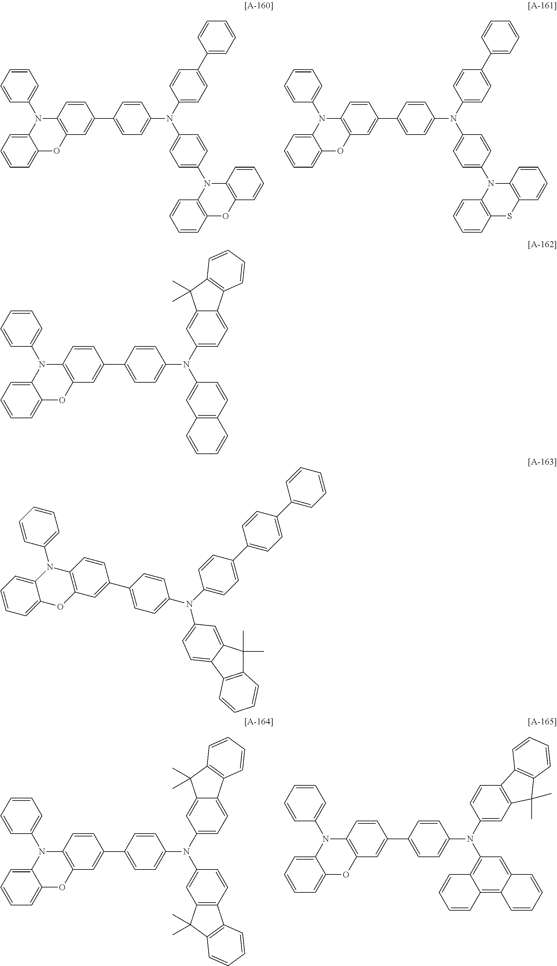


- The compound for an organic optoelectronic device may be represented by one of the following Chemical Formulae B-1 to B-81, but is not limited thereto.
-


- The compound for an organic optoelectronic device may be represented by the following Chemical Formulae C-1 to C-54, but is not limited thereto.
-


- The compound for an organic optoelectronic device may be represented by the following Chemical Formulae D-1 to D-36, but is not limited thereto.
-


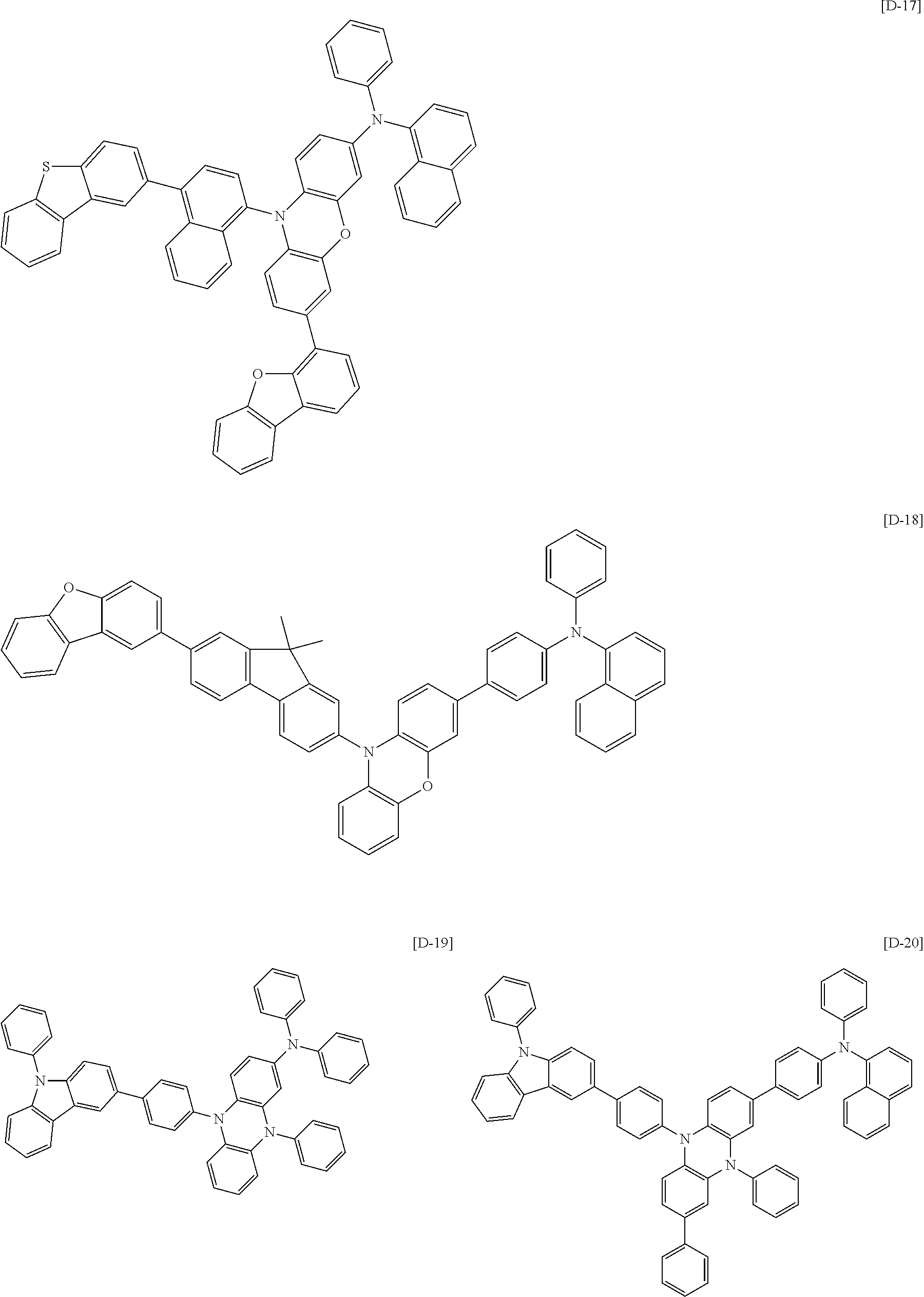


- The compound for an organic optoelectronic device may be represented by the following Chemical Formulae E-1 to E-18, but is not limited thereto.
-


- When the compound for an organic optoelectronic device according to the above-described embodiment is used in an electron blocking layer (or hole transport layer (HTL)) of an organic light emitting diode, electron inhibiting properties of important characteristics may tend to be deteriorated due to a functional group having electron characteristics in the molecule. Therefore, in an embodiment, the compound may not include a functional group having electron characteristics so that it may be used in an electron blocking layer. Examples of the functional group having electron characteristics may be benzoimidazole, pyridine, pyrazine, pyrimidine, triazine, quinoline, isoquinoline, and the like. The above descriptions are limited to using the compound in an electron blocking layer or hole transport layer (HTL) (or hole injection layer (HIL)).
- The compound for an organic optoelectronic device including the above compounds may have a glass transition temperature of greater than or equal to 110° C. and a thermal decomposition temperature of greater than or equal to 400° C., indicating improved thermal stability. Thereby, it may be possible to produce an organic optoelectronic device having a high efficiency.
- The compound for an organic optoelectronic device including the above compounds may play a role for emitting light or injecting and/or transporting holes, and also act as a light emitting host with an appropriate dopant. In other words, the compound for an organic optoelectronic device may be used as a phosphorescent or fluorescent host material, a blue light emitting dopant material, or an electron transport material.
- The compound for an organic optoelectronic device according to an example embodiment may be used for an organic thin layer, and it may improve the life-span characteristic, efficiency characteristic, electrochemical stability, and thermal stability of an organic photoelectric device, and decrease the driving voltage.
- Another example embodiment provides an organic optoelectronic device that includes the compound for an organic optoelectronic device according to an embodiment. The organic optoelectronic device may include, e.g., an organic photoelectric device, an organic light emitting diode, an organic solar cell, an organic transistor, an organic photo-conductor drum, an organic memory device, or the like. For example, the compound for an organic optoelectronic device according to an example embodiment may be included in an electrode or an electrode buffer layer in the organic solar cell to improve the quantum efficiency, and it may be used as an electrode material for a gate, a source-drain electrode, or the like in the organic transistor.
- Another embodiment includes an anode, a cathode, and at least one or more organic thin layer between the anode and the cathode, and at least one of the organic thin layers may include the compound for an organic optoelectronic device according to an example embodiment.
- The organic thin layer that may include the compound for an organic optoelectronic device may include a layer selected from an emission layer, a hole transport layer (HTL), a hole injection layer (HIL), an electron transport layer (ETL), an electron injection layer (EIL), a hole blocking layer, and a combination thereof. The at least one layer includes the compound for an organic optoelectronic device according to an example embodiment. Particularly, the compound for an organic optoelectronic device according to an example embodiment may be included in an electron transport layer (ETL) or electron injection layer (EIL). In addition, when the compound for an organic optoelectronic device is included in the emission layer, the compound for an organic optoelectronic device may be included as a phosphorescent or fluorescent host, and particularly, as a fluorescent blue dopant material.
-
FIGS. 1 to 5 illustrate cross-sectional views showing organic light emitting diodes including the compound for an organic optoelectronic device according to example embodiments. - Referring to
FIGS. 1 to 5 , organiclight emitting diodes thin layer 105 interposed between ananode 120 and acathode 110. - The
anode 120 may include an anode material having a large work function to help hole injection into an organic thin layer. The anode material may include, e.g., a metal such as nickel, platinum, vanadium, chromium, copper, zinc, gold, or alloys thereof; a metal oxide such as zinc oxide, indium oxide, indium tin oxide (ITO), or indium zinc oxide (IZO); a bonded metal and oxide such as ZnO:Al or SnO2:Sb; or a conductive polymer such as poly(3-methylthiophene), poly[3,4-(ethylene-1,2-dioxy)thiophene] (PEDT), polypyrrole, or polyaniline, etc. In an implementation, a transparent electrode including indium tin oxide (ITO) may be included as an anode. - The
cathode 110 may include a cathode material having a small work function to help electron injection into an organic thin layer. The cathode material may include, e.g., a metal such as magnesium, calcium, sodium, potassium, titanium, indium, yttrium, lithium, gadolinium, aluminum, silver, tin, lead, or alloys thereof; or a multi-layered material such as LiF/Al, Liq/Al, LiO2/Al, LiF/Ca, LiF/Al, or BaF2/Ca, etc. In an implementation, a metal electrode including aluminum may be included as a cathode. - Referring to
FIG. 1 , in an example embodiment the organicphotoelectric device 100 includes an organicthin layer 105 including only anemission layer 130. - Referring to
FIG. 2 , in an example embodiment a double-layered organicphotoelectric device 200 includes an organicthin layer 105 including anemission layer 230 including an electron transport layer (ETL), and a hole transport layer (HTL) 140. As shown inFIG. 2 , the organicthin layer 105 includes a double layer of theemission layer 230 and hole transport layer (HTL) 140. Theemission layer 130 also functions as an electron transport layer (ETL), and the hole transport layer (HTL) 140 layer may have an excellent binding property with a transparent electrode such as ITO or an excellent hole transport capability. - Referring to
FIG. 3 , in an example embodiment a three-layered organicphotoelectric device 300 includes an organicthin layer 105 including an electron transport layer (ETL) 150, anemission layer 130, and a hole transport layer (HTL) 140. Theemission layer 130 is independently installed, and layers having an excellent electron transport capability or an excellent hole transport capability may be separately stacked. - As shown in
FIG. 4 , in an example embodiment a four-layered organicphotoelectric device 400 includes an organicthin layer 105 including an electron injection layer (EIL) 160, anemission layer 130, a hole transport layer (HTL) 140, and a hole injection layer (HIL) 170 that may enhance adherence with the cathode of ITO. - As shown in
FIG. 5 , in an example embodiment a five layered organicphotoelectric device 500 includes an organicthin layer 105 including an electron transport layer (ETL) 150, anemission layer 130, a hole transport layer (HTL) 140, and a hole injection layer (HIL) 170, and further includes an electron injection layer (EIL) 160, which may provide a low voltage. - In
FIGS. 1 to 5 , the organicthin layer 105 including at least one selected from an electron transport layer (ETL) 150, an electron injection layer (EIL) 160, emission layers 130 and 230, a hole transport layer (HTL) 140, a hole injection layer (HIL) 170, and combinations thereof includes a compound for an organic optoelectronic device according to an embodiment. The compound for an organic optoelectronic device may be used for an electron transport layer (ETL) 150 including the electron transport layer (ETL) 150 or electron injection layer (EIL) 160. When it is used for the electron transport layer (ETL), it may be possible to provide an organic photoelectric device having a simpler structure by omitting an additional hole blocking layer (not shown). - Furthermore, when the compound for an organic photoelectric device is included in the emission layers 130 and 230, the compound for the organic photoelectric device may be included as a phosphorescent or fluorescent host or a fluorescent blue dopant.
- The organic light emitting diode may be fabricated by, e.g.: forming an anode on a substrate; forming an organic thin layer in accordance with a dry coating method such as evaporation, sputtering, plasma plating, and ion plating, or a wet coating method such as spin coating, dipping, and flow coating; and providing a cathode thereon.
- Another example embodiment provides a display device including an organic photoelectric device according to an embodiment.
- The following Examples and Comparative Examples are provided in order to highlight characteristics of one or more embodiments, but it will be understood that the Examples and Comparative Examples are not to be construed as limiting the scope of the embodiments, nor are the Comparative Examples to be construed as being outside the scope of the embodiments. Further, it will be understood that the embodiments are not limited to the particular details described in the Examples and Comparative Examples.
- (Preparation of Compound for Organic Optoelectronic Device)
- Synthesis of Intermediate
- Synthesis of Intermediate M-1
-

- 30 g (163.8 mmol) of phenoxazine, 30.8 g (196.6 mmol) of bromobenzene, 23.6 g (245.8 mmol) of sodium t-butoxide, and 1.0 g (4.92 mmol) of tri-tert-butylphosphine were dissolved in 330 ml of toluene, 0.94 g (1.64 mmol) of Pd(dba)2 was added thereto, and the mixture was agitated for 6 hours under a nitrogen atmosphere while being refluxed. When the reaction was complete, the resultant was extracted with ethyl acetate and distilled water, an organic layer obtained therefrom was dried with magnesium sulfate and filtered, and the filtered solution was concentrated under a reduced pressure. Then, the concentrated product was purified with n-hexane/dichloromethane (7:3 of a volume ratio) through silica gel column chromatography, obtaining 40.3 g of a white solid compound, an intermediate M-1 (95% of a yield).
- LC-Mass (calcd.: 259.10 g/mol, measured.: M+1=260 g/mol)
- Synthesis of Intermediate M-2
-

- 50 g (250.9 mmol) of phenothiazine, 47.3 g (301.1 mmol) of bromobenzene, 36.2 g (376.4 mmol) of sodium t-butoxide, and 1.52 g (7.53 mmol) of tri-tert-butylphosphine were dissolved in 500 ml of toluene, 1.44 g (2.51 mmol) of Pd(dba)2 was added thereto, and the mixture was agitated for 6 hours under a nitrogen atmosphere while being refluxed. When the reaction was complete, the resultant was extracted with ethyl acetate and distilled water, an organic layer obtained therefrom was dried with magnesium sulfate and filtered, and the filtered solution was concentrated under a reduced pressure. The concentrated product was purified with n-hexane/dichloromethane (7:3 of a volume ratio) through silica gel column chromatography, obtaining 61.7 g of a white solid compound, an intermediate M-2 (89% of a yield).
- LC-Mass (calcd.: 275.08 g/mol, measured.: M+1=276 g/mol)
- Synthesis of Intermediate M-3
-

- 40 g (154.2 mmol) of the intermediate M-1 was dissolved in 400 ml of chloroform, and another solution prepared by dissolving 27.4 g (154.2 mmol) of N-bromosuccinimide in 120 ml of dimethylformamide was slowly added thereto for 4 hours, while the former solution was agitated at 0° C. The reactant was agitated at room temperature for 2 hours and then extracted with distilled water and dichloromethane. An organic layer obtained therefrom was dried with potassium carbonate and filtered, and the filtered solution was concentrated under a reduced pressure. The concentrated product was purified with n-hexane through silica gel column chromatography, obtaining 31.8 g of a white solid compound, an intermediate M-3 (61% of a yield).
- LC-Mass (calcd.: 337.01 g/mol, measured.: M+1=339 g/mol)
- Synthesis of Intermediate M-4
-

- 60 g (217.9 mmol) of the intermediate M-2 was dissolved in 600 ml of chloroform, and a solution prepared by dissolving 38.8 g (38.8 mmol) of N-bromosuccinimide in 180 ml of dimethylformamide was slowly added thereto for 4 hours, while the former solution was agitated at 0° C. The reactant was agitated at room temperature for 2 hours and extracted with distilled water and dichloromethane. An organic layer obtained therefrom was dried with potassium carbonate and filtered, and the filtered solution was concentrated under a reduced pressure. The concentrated product was purified with n-hexane through silica gel column chromatography, obtaining 48.6 g of a white solid compound, an intermediate M-4 (63% of a yield).
- LC-Mass (calcd.: 352 g/mol, measured.: M+1=355 g/mol)
- Synthesis of Intermediate M-5
-

- 20 g (59.1 mmol) of the intermediate M-3, 9.2 g (59.1 mmol) of 4-chlorophenylboronic acid, and 0.68 g (0.59 mmol) of tetrakistriphenylphosphine palladium dissolved in 200 ml of toluene under a nitrogen atmosphere in a flask and, 100 ml of an aqueous solution in which 13 g (88.7 mmol) of potassium carbonate was dissolved was added thereto, and the mixture was agitated for 8 hours while being refluxed. When the reaction was complete, the resultant was extracted with ethyl acetate, the extracted solution was dried with magnesium sulfate and filtered, and the filtered solution was concentrated under a reduced pressure. The concentrated product was purified with n-hexane/dichloromethane (8:2 of a volume ratio) through silica gel column chromatography, obtaining 19.2 g of a white solid compound, an intermediate M-5 (88% of a yield).
- LC-Mass (calcd.: 369.00 g/mol, measured.: M+1=370 g/mol)
- Synthesis of Intermediate M-6
-

- 20.9 g (59.1 mmol) of the intermediate M-4, 9.2 g (59.1 mmol) of 4-chlorophenylboronic acid, and 0.68 g (0.59 mmol) of tetrakistriphenylphosphine palladium were dissolved in 200 ml of toluene under a nitrogen atmosphere in a flask, 100 ml of an aqueous solution in which 13 g (88.7 mmol) of potassium carbonate was dissolved was added thereto, and the mixture was agitated for 8 hours while being refluxed. When the reaction was complete, the resultant was extracted with ethyl acetate, an extracted solution was dried with magnesium sulfate and filtered, and the filtered solution was concentrated under a reduced pressure. The concentrated product was purified with n-hexane/dichloromethane (8:2 of a volume ratio) through silica gel column chromatography, obtaining 20.5 g of a white solid compound, an intermediate M-6 (90% of a yield).
- LC-Mass (calcd.: 386.00 g/mol, measured.: M+1=387 g/mol)
- Synthesis of Intermediate M-7
-

- 20 g (118.2 mmol) of 4-aminobiphenyl, 24.8 g (106.4 mmol) of 4-bromobiphenyl, 15.3 g (159.6 mmol) of sodium t-butoxide, and 0.65 g (3.19 mmol) of tri-tert-butylphosphine were dissolved in 590 ml of toluene, 0.61 g (1.06 mmol) of Pd(dba)2 was added thereto, and the mixture was agitated under a nitrogen atmosphere for 6 hours while being refluxed. When the reaction was complete, the resultant was extracted with ethyl acetate and distilled water, an organic layer obtained therefrom was dried with magnesium sulfate and filtered, and the filtered solution was concentrated under a reduced pressure. The concentrated product was purified with n-hexane/dichloromethane (7:3 of a volume ratio) through silica gel column chromatography, obtaining 26 g of a white solid compound, an intermediate M-7 (76% of a yield).
- LC-Mass (calcd.: 321.00 g/mol, measured.: M+1=321.41 g/mol)
- Synthesis of Intermediate M-8
-

- 20 g (118.2 mmol) of 4-aminobiphenyl, 29.1 g (106.4 mmol) of 2-bromo-9,9-dimethylfluorene, 15.3 g (159.6 mmol) of sodium t-butoxide, and 0.65 g (3.19 mmol) of tri-tert-butylphosphine were dissolved in 590 ml of toluene, 0.61 g (1.06 mmol) of Pd(dba)2 was added thereto, and the mixture was agitated for 6 hours under a nitrogen atmosphere while being refluxed. When the reaction was complete, the resultant was extracted with ethyl acetate and distilled water, an organic layer obtained therefrom was dried with magnesium sulfate and filtered, and the filtered solution was concentrated under a reduced pressure. The concentrated product was purified with n-hexane/dichloromethane (7:3 of a volume ratio) through silica gel column chromatography, obtaining 28.5 g of a white solid compound, an intermediate M-8 (74% of a yield).
- LC-Mass (calcd.: 361.00 g/mol, measured.: M+1=362.00 g/mol)
- Synthesis of Intermediate M-9
-

- 20 g (94.4 mmol) of 4-dibenzofuranboronic acid, 28 g (99.2 mmol) of 1-bromo-4-iodobenzene, and 1.08 g (0.94 mmol) of tetrakistriphenylphosphine palladium were dissolved in 240 ml of toluene and 120 ml of ethanol under a nitrogen atmosphere in a flask, 120 ml of an aqueous solution in which 28 g (188.8 mmol) of potassium carbonate was dissolved was added thereto, and the mixture was agitated for 12 hours while being refluxed. When the reaction was complete, the resultant was extracted with ethyl acetate, the extracted solution was dried with magnesium sulfite and filtered, and the filtered solution was concentrated under a reduced pressure. The concentrated product was purified with n-hexane/dichloromethane (9:1 of a volume ratio) through silica gel column chromatography, obtaining 27 g of a white solid compound, an intermediate M-9 (89% of a yield).
- LC-Mass (calcd.: 322.00 g/mol, measured.: M+1=323 g/mol)
- Synthesis of Intermediate M-10
-

- 30 g (178.4 mmol) of dibenzofuran was dissolved in 270 g of acetic acid in a round-bottomed flask, and a solution prepared by dissolving 29 g (181.5 mmol) of bromine in 6 g of acetic acid was slowly added thereto at 50° C. for 4 hours. The reaction solution was additionally agitated at 50° C. for 8 hours, cooled down, and added to distilled water. An orange solid was dissolved in dichloromethane, the solution was cleaned with a sodium thiosulfite aqueous solution, an organic layer obtained therefrom was dried with magnesium sulfite and filtered, and the filtered solution was concentrated under a reduced pressure. The concentrated product was recrystallized with dichloromethane/n-hexane, obtaining 10.1 g of a white solid compound, an intermediate M-10 (23% of a yield).
- GC-Mass (calcd.: 245.97 g/mol, measured.: M+1=246 g/mol)
- Synthesis of Intermediate M-11
-

- 20 g (127.9 mmol) of 4-chlorophenylboronic acid, 30.0 g (121.5 mmol) of the intermediate M-10, and 1.48 g (1.28 mmol) of tetrakistriphenylphosphine palladium were dissolved in 320 ml of toluene and 160 ml of ethanol in a flask under a nitrogen atmosphere, 160 ml of an aqueous solution in which 37.7 g (255.8 mmol) of potassium carbonate was dissolved was added thereto, and the mixture was agitated for 12 hours while being refluxed. When the reaction was complete, the resultant was extracted with ethyl acetate, the extracted solution was dried with magnesium sulfite and filtered, and the filtered solution was concentrated under a reduced pressure. The concentrated product was purified with n-hexane/dichloromethane (9:1 volume ratio) through silica gel column chromatography, obtaining 28.1 g of a white solid compound, an intermediate M-11 (83% of a yield).
- LC-Mass (calcd.: 278.05 g/mol, measured.: M+1=279 g/mol)
- Synthesis of Intermediate M-12
-

- 50 g (155.18 mmol) of 3-bromo-9-phenyl-9H-carbazole, 3.41 g (4.65 mmol) of Pd(dip)Cl2, 51.32 g (201.8 mmol) of bis(pinacolato)diboron, and 45.8 g (465.5 mmol) of potassium acetate were dissolved in 520 ml of 1,4-dioxane. The reactant was reflux-agitated under a nitrogen atmosphere for 12 hours and then three times extracted with dichloromethane and distilled water. The extracted solution was dried with magnesium sulfite and filtered, and the filtered solution was concentrated under a reduced pressure. The concentrated product was purified with n-hexane/dichloromethane (7:3 of a volume ratio) through silica gel column chromatography, obtaining 43 g of a white solid compound, an intermediate M-12 (75% of a yield).
- LC-Mass (calcd.: 369.19 g/mol, measured.: M+1=370 g/mol)
- Synthesis of Intermediate M-13
-

- 40 g (108.3 mmol) of the intermediate M-12, 30.6 g (108.3 mmol) of 1-bromo-4-iodobenzene, and 1.25 g (1.08 mmol) of tetrakistriphenylphosphine palladium were dissolved in 270 ml of toluene and 135 ml of ethanol in a flask under a nitrogen atmosphere. Then, 135 ml of an aqueous solution in which 31.9 g (58.9 mmol) of potassium carbonate was added to the solution, and the mixture was agitated for 12 hours while being refluxed. When the reaction was complete, the resultant was extracted with ethyl acetate, the extracted solution was dried with magnesium sulfite and filtered, and the filtered solution was concentrated under a reduced pressure. The concentrated product was purified with n-hexane/dichloromethane (7:3 of a volume ratio) through silica gel column chromatography, obtaining 35 g of a white solid compound, an intermediate M-13 (81% of a yield).
- LC-Mass (calcd.: 398.29 g/mol, measured.: M+1=399 g/mol)
- Synthesis of Intermediate M-14
-

- 10 g (42.9 mmol) of 4-bromobiphenyl was dissolved in 143 ml of anhydrous tetrahydrofuran in a round-bottomed flask under a nitrogen atmosphere. The solution was cooled down to −78° C. and agitated, 27 ml (42.9 mmol) of a 1.6 M n-butyl lithium hexane solution was slowly added thereto, and the mixture was reacted at −78° C. for 1 hour. 8.5 g (47.2 mmol) of phenazine was dissolved in 143 ml of anhydrous tetrahydrofuran in a round-bottomed flask under a nitrogen atmosphere. The solution was cooled down to −78° C. and agitated, a 4-biphenyl lithium solution was slowly added thereto, and the mixture was heated up to room temperature and reacted for 12 hours. Then, distilled water was added to the resultant to complete the reaction, the reaction solution was concentrated under a reduced pressure to remove tetrahydrofuran and then extracted with toluene/distilled water, an organic layer obtained therefrom was dried with sodium sulfate and filtered, and the filtered solution was concentrated under a reduced pressure. The concentrated product was recrystallized under nitrogen and then purified with toluene/ethanol, obtaining 7.2 g of a desired compound, an intermediate M-14 (50% of a yield). The obtained product was refrigerated under nitrogen.
- LC-Mass (calcd.: 336.00 g/mol, measured.: M+1=337.00 g/mol)
- Synthesis of Intermediate M-15
-

- 18.7 g (100 mmol) of 4-bromo-1,2-diaminobenzene and 22 g (200 mmol) of catechol were heated to 100° C. and agitated under nitrogen atmosphere in a round-bottomed flask until completely dissolved, and the solution was heated up to 180° C. and then heated and agitated for 48 hours. The resultant was cooled down to 80° C., toluene and distilled water were added thereto, and the mixture was agitated for 1 hour under a nitrogen atmosphere. The resultant was extracted with toluene and distilled water, an organic layer obtained therefrom was dried with sodium sulfate and filtered, and the filtered solution was concentrated under a reduced pressure. The concentrated product was recrystallized and purified with toluene/ethanol under nitrogen, obtaining 15.9 g of a compound, an intermediate M-15 (61% of a yield). The obtained product was refrigerated under nitrogen.
- LC-Mass (calcd.: 260.00 g/mol, measured.: M+1=261.00 g/mol)
- Synthesis of Intermediate M-16
-

- 10 g (38.3 mmol) of the intermediate M-15, 46.9 g (229.8 mmol) of iodobenzene, and 21.1 g (153.2 mmol) of potassium carbonate were dissolved in 130 ml of 1,2-dichlorobenzene, 0.49 g (7.66 mmol) of copper powder and 2.02 g (7.66 mmol) of 18-crown-6-ether were added thereto, and the mixture was agitated at 180° C. for 24 hours under a nitrogen atmosphere. When the reaction was complete, the resultant was extracted with dichloromethane and distilled water, an organic layer obtained therefrom was dried with magnesium sulfate and filtered, and the filtered solution was concentrated under a reduced pressure. The concentrated product was purified with n-hexane/dichloromethane (7:3 of a volume ratio) through silica gel column chromatography, obtaining 13.5 g of a compound, an intermediate M-16 (85% of a yield).
- LC-Mass (calcd.: 412.00 g/mol, measured.: M+1=413.00 g/mol)
-

- 10 g (27.0 mmol) of the intermediate M-5, 8.7 g (27.0 mmol) of the intermediate M-7, 3.9 g (40.5 mmol) of sodium t-butoxide, and 0.16 g (0.81 mmol) of tri-tert-butylphosphine were dissolved in 270 ml of toluene, 0.15 g (0.27 mmol) of Pd(dba)2 was added thereto, and the mixture was agitated under a nitrogen atmosphere for 12 hours while being refluxed. When the reaction was complete, the resultant was extracted with ethyl acetate and distilled water, an organic layer obtained therefrom was dried with magnesium sulfate and filtered, and the filtered solution was concentrated under a reduced pressure. The concentrated product was purified with n-hexane/dichloromethane (7:3 of a volume ratio) through silica gel column chromatography, obtaining 15.7 g of a white solid compound, an intermediate A-140 (89% of a yield).
- LC-Mass (calcd.: 654.00 g/mol, measured.: M+1=655.00 g/mol)
-

- 10 g (27.0 mmol) of the intermediate M-5, 9.8 g (27.0 mmol) of the intermediate M-8, 3.9 g (40.5 mmol) of sodium t-butoxide, and 0.16 g (0.81 mmol) of tri-tert-butylphosphine were dissolved in 270 ml of toluene, 0.15 g (0.27 mmol) of Pd(dba)2 was added thereto, and the mixture was agitated under a nitrogen atmosphere for 12 hours while being refluxed. When the reaction was complete, the resultant was extracted with ethyl acetate and distilled water, an organic layer obtained therefrom was dried with magnesium sulfate and filtered, and the filtered solution was concentrated under a reduced pressure. The concentrated product was purified with n-hexane/dichloromethane (7:3 of a volume ratio) through silica gel column chromatography, obtaining 17.1 g of a white solid compound, an intermediate A-142 (91% of a yield).
- LC-Mass (calcd.: 694.00 g/mol, measured.: M+1=695.00 g/mol)
-

- 10.4 g (27.0 mmol) of the intermediate M-6, 8.7 g (27.0 mmol) of the intermediate M-7, 3.9 g (40.5 mmol) of sodium t-butoxide, and 0.16 g (0.81 mmol) of tri-tert-butylphosphine were dissolved in 270 ml of toluene, 0.15 g (0.27 mmol) of Pd(dba)2 was added thereto, and the mixture was agitated under a nitrogen atmosphere for 12 hours while being refluxed. When the reaction was complete, the resultant was extracted with ethyl acetate and distilled water, an organic layer obtained therefrom was dried with magnesium sulfate and filtered, and the filtered solution was concentrated under a reduced pressure. The concentrated product was purified with n-hexane/dichloromethane (7:3 of a volume ratio) through silica gel column chromatography, obtaining 16.5 g of a white solid compound, an intermediate A-216 (91% of a yield).
- LC-Mass (calcd.: 670.00 g/mol, measured.: M+1=671.00 g/mol)
-

- 10.4 g (27.0 mmol) of the intermediate M-6, 9.8 g (27.0 mmol) of the intermediate M-8, 3.9 g (40.5 mmol) of sodium t-butoxide, and 0.16 g (0.81 mmol) of tri-tert-butylphosphine were dissolved in 270 ml of toluene, 0.15 g (0.27 mmol) of Pd(dba)2 was added thereto, and the mixture was agitated under a nitrogen atmosphere for 12 hours while being refluxed. When the reaction was complete, the resultant was extracted with ethyl acetate and distilled water, an organic layer obtained therefrom was dried with magnesium sulfate and filtered, and the filtered solution was concentrated under a reduced pressure. The concentrated product was purified with n-hexane/dichloromethane (7:3 of a volume ratio) through silica gel column chromatography, obtaining 16.9 g of a white solid compound, an intermediate A-217 (88% of a yield).
- LC-Mass (calcd.: 710.00 g/mol, measured.: M+1=711.00 g/mol)
-

- 10.8 g (27.0 mmol) of the intermediate M-13, 5 g (27.0 mmol) of phenoxazine, 3.9 g (40.5 mmol) of sodium t-butoxide, and 0.16 g (0.81 mmol) of tri-tert-butylphosphine were dissolved in 270 ml of toluene, 0.15 g (0.27 mmol) of Pd(dba)2 was added thereto, and the mixture was agitated under a nitrogen atmosphere for 12 hours while being refluxed. When the reaction was complete, the resultant was extracted with ethyl acetate and distilled water, an organic layer obtained therefrom was dried with magnesium sulfate and filtered, and the filtered solution was concentrated under a reduced pressure. The concentrated product was purified with n-hexane/dichloromethane (7:3 of a volume ratio) through silica gel column chromatography, obtaining 12.4 g of a white solid compound, an intermediate B-1 (92% of a yield).
- LC-Mass (calcd.: 500.00 g/mol, measured.: M+1=501.00 g/mol)
-

- 7.5 g (27.0 mmol) of the intermediate M-11, 5.4 g (27.0 mmol) of phenothiazine, 3.9 g (40.5 mmol) of sodium t-butoxide, and 0.16 g (0.81 mmol) of tri-tert-butylphosphine were dissolved in 270 ml of toluene, 0.15 g (0.27 mmol) of Pd(dba)2 was added thereto, and the mixture was agitated under a nitrogen atmosphere for 12 hours while being refluxed. When the reaction was complete, the resultant was extracted with ethyl acetate and distilled water, an organic layer obtained therefrom was dried with magnesium sulfate and filtered, and the filtered solution was concentrated under a reduced pressure. The concentrated product was purified with n-hexane/dichloromethane (7:3 of a volume ratio) through silica gel column chromatography, obtaining 10.8 g of a white solid compound, an intermediate B-35 (91% of a yield).
- LC-Mass (calcd.: 441.00 g/mol, measured.: M+1=442.00 g/mol)
-

- 7.5 g (27.0 mmol) of the intermediate M-11, 9.1 g (27.0 mmol) of the intermediate M-14, 3.9 g (40.5 mmol) of sodium t-butoxide, and 0.16 g (0.81 mmol) of tri-tert-butylphosphine were dissolved in 270 ml of toluene, 0.15 g (0.27 mmol) of Pd(dba)2 was added thereto, and the mixture was agitated under a nitrogen atmosphere for 12 hours while being refluxed. When the reaction was complete, the resultant was extracted with ethyl acetate and distilled water, an organic layer obtained therefrom was dried with magnesium sulfate and filtered, and the filtered solution was concentrated under a reduced pressure. The concentrated product was purified with n-hexane/dichloromethane (7:3 of a volume ratio) through silica gel column chromatography, obtaining 14 g of a white solid compound, an intermediate C-35 (90% of a yield).
- LC-Mass (calcd.: 576.00 g/mol, measured.: M+1=577.00 g/mol)
-

- 9.0 g (21.6 mmol) of the intermediate M-16, 6.2 g (21.6 mmol) of triphenylamine-4-boronic acid, and 0.26 g (0.108 mmol) of tetrakistriphenylphosphine palladium were dissolved in 216 ml of toluene under a nitrogen atmosphere in a flask. Subsequently, 150 ml of an aqueous solution in which 6.4 g (11.8 mmol) of potassium carbonate was dissolved was added to the solution, and the mixture was agitated for 12 hours while being refluxed. When the reaction was complete, the resultant was extracted with toluene, the extracted solution was dried with magnesium sulfate and filtered, and the filtered solution was concentrated under a reduced pressure. The concentrated product was purified with n-hexane/dichloromethane (7:3 of a volume ratio) through silica gel column chromatography, obtaining 10.6 g of a white solid compound A-237 (85% of a yield).
- LC-Mass (calcd.: 577.00 g/mol, measured.: M+1=578.00 g/mol)
- A glass substrate coated with ITO (Indium tin oxide) to form a 1500 Å-thick thin film was cleaned with a distilled water ultrasonic wave. After cleaning with distilled water, the glass substrate was ultra sonic wave-cleaned with a solvent such as isopropyl alcohol, acetone, methanol, and the like and moved to a plasma cleaner and then cleaned by using oxygen plasma for 5 minutes and moved to a vacuum-depositor. This ITO transparent electrode was used as an anode, 4,4′-bis[N-[4-{N,N-bis(3-methylphenyl)amino}-phenyl]-N-phenylamino]biphenyl (DNTPD) was vacuum-deposited on the ITO substrate to form a 600 Å-thick hole injection layer (HIL). Subsequently, the compound according to Example 1 was vacuum-deposited to form a 300 Å-thick hole transport layer (HTL). On the hole transport layer (HTL), a 250 Å-thick emission layer was vacuum-deposited by doping 9,10-di-(2-naphthyl)anthracene (ADN) as a host with 3 wt % of 2,5,8,11-tetra(tert-butyl)perylene (TBPe) as a dopant.
- Subsequently, Alq3 was vacuum-deposited to form a 250 Å-thick electron transport layer (ETL) on the emission layer. On the electron transport layer (ETL), 10 Å-thick LiF and 1000 Å-thick Al were sequentially vacuum-deposited to form a cathode, manufacturing an organic light emitting diode.
- The organic light emitting diode has a structure of five organic thin layers and specifically, a structure of:
-
- 1000 Å Al/10 Å LiF/250 Å Alq3/250 Å EML[ADN:TBPe=97:3]/300 Å HTL/600 Å DNTPD/1500 Å ITO.
- An organic light emitting diode was manufactured according to the same method as Example 9 except for using the compound according to Example 2 instead of the compound according to Example 1.
- An organic light emitting diode was manufactured according to the same method as Example 9 except for using the compound according to Example 3 instead of the compound according to Example 1.
- An organic light emitting diode was manufactured according to the same method as Example 9 except for using the compound according to Example 4 instead of the compound according to Example 1.
- An organic light emitting diode was manufactured according to the same method as Example 9 except for using the compound according to Example 5 instead of the compound according to Example 1.
- An organic light emitting diode was manufactured according to the same method as Example 9 except for using the compound according to Example 6 instead of the compound according to Example 1.
- An organic light emitting diode was manufactured according to the same method as Example 9 except for using the compound according to Example 7 instead of the compound according to Example 1.
- An organic light emitting diode was manufactured according to the same method as Example 9 except for using the compound according to Example 8 instead of the compound according to Example 1.
- An organic light emitting diode was manufactured according to the same method as Example 9 except for using NPB instead of the compound according to Example 1. The NPB has a structure shown below.
- An organic light emitting diode was manufactured according to the same method as Example 9 except for using HT1 instead of the compound according to Example 1. The HT1 has a structure shown below.
- An organic light emitting diode was manufactured according to the same method as Example 9 except for using HT2 instead of the compound according to Example 1. The HT1 has a structure shown below.
- An organic light emitting diode was manufactured according to the same method as Example 9 except for using HT3 instead of the compound according to Example 1. The HT3 has a structure shown below.
- The DNTPD, ADN, TBPe, NPB, HT1, HT2, and HT3 used for an organic light emitting diode respectively have a structure shown below.
-

- (Analysis and Characteristics Measurement of Compound)
- 1H-NMR Result Analysis
- The molecular weights of the intermediates M-1 to M-8 and the compounds according to Examples 1 to 2 were measured by using LC-MS for a structure analysis, and 1H-NMR thereof was measured by using a 300 MHz NMR equipment after dissolved in a CD2Cl2 solvent.
-
FIG. 6 shows 1H-NMR data of the compound A-140 according to Example 1,FIG. 7 shows 1H-NMR data of the compound A-142 according to Example 2,FIG. 8 shows 1H-NMR data of the compound A-216 according to Example 3, andFIG. 9 shows 1H-NMR data of the compound A-217 according to Example 4. - Referring to
FIGS. 6 , 7, 8, and 9, desired compounds were synthesized. - (Performance Measurement of Organic Light Emitting Diode)
- Current density and luminance changes depending on voltage and luminous efficiency of each organic light emitting diode according to Examples 9 to 16 and Comparative Examples 1 to 4 were measured. The measurements were specifically performed in the following method. The results were provided in the following Table 1.
- (1) Measurement of Current Density Change Depending on Voltage Change
- The manufactured organic light emitting diodes were measured for current value flowing in the unit device, while increasing the voltage from 0V to 10V using a current-voltage meter (Keithley 2400), and the measured current value was divided by an area to provide the result.
- (2) Measurement of Luminance Change Depending on Voltage Change
- The organic light emitting diodes were measured for luminance, while increasing the voltage faint 0V to 10V using a luminance meter (Minolta Cs-1000A).
- (3) Measurement of Luminous Efficiency
- Current efficiency (cd/A) and electric power efficiency (lm/W) at the same current density (10 mA/cm2) were calculated by using the luminance, current density, and voltages from the items (1) and (2).
-
TABLE 1 Compound used Volt- Color Effi- Half-life in hole transport age (EL ciency life-span (h) Devices layer (HTL) (V) color) (cd/A) at 1000 cd/m2 Example 9 A-140 6.2 Blue 5.7 1,510 Example 10 A-142 6.2 Blue 5.8 1,490 Example 11 A-216 6.3 Blue 5.6 1,360 Example 12 A-217 6.3 Blue 5.8 1,340 Example 13 B-1 6.5 Blue 4.9 1,250 Example 14 B-35 6.6 Blue 5.0 1,140 Example 15 C-35 6.6 Blue 5.0 1,210 Example 16 C-237 6.4 Blue 5.5 1,290 Comparative NPB 7.1 Blue 4.9 1,250 Example 1 Comparative HT1 7.0 Blue 4.1 1,080 Example 2 Comparative HT2 6.8 Blue 4.4 1,210 Example 3 Comparative HT3 6.6 Blue 4.1 1,050 Example 4 Current Density: 10 mA/cm2 - From the results of the Table 1, the organic light emitting diodes according to Example 9 to 16 showed low driving voltages and improved efficiency.
- In addition, the organic light emitting diodes according to Examples 9 to 11 and 16 showed improved half-life life-spans compared with the organic light emitting diodes according to Comparative Examples 1 to 4 and, particularly, the organic light emitting diode according to Example 9 showed a half-life life-span of 1,380 hours (h), which was greater than or equal to 20% improved half-life life-span compared with 1,250 hours of the organic light emitting diode according to Comparative Example 1. Considering that life-span of a device is important for commercial availability, the half-life life-span improvement of the devices according to the Examples indicates suitability for commercial application.
- By way of summation and review, examples of an organic optoelectronic device include an organic photoelectric device, an organic light emitting diode, an organic solar cell, an organic photo conductor drum, an organic transistor, and the like, Such devices may use a hole injecting or transport material, an electron injecting or transport material, and/or a light emitting material.
- An organic light emitting diode (OLED) has drawn attention due to a demand for flat panel displays. In general, organic light emission refers to conversion of electrical energy into photo-energy.
- Such an organic light emitting diode converts electrical energy into light by applying current to an organic light emitting material. It has a structure in which a functional organic material layer is interposed between an anode and a cathode. The organic material layer may include a multi-layer including different materials, for example a hole injection layer (HIL), a hole transport layer (HTL), an emission layer, an electron transport layer (ETL), and an electron injection layer (EIL), which may improve efficiency and stability of an organic photoelectric device.
- In such an organic light emitting diode, when a voltage is applied between an anode and a cathode, holes from the anode and electrons from the cathode are injected to an organic material layer and recombined to generate excitons having high energy. The generated excitons generate light having certain wavelengths while shifting to a ground state.
- A phosphorescent light emitting material may be used for a light emitting material of an organic photoelectric device in addition to the fluorescent light emitting material. Such a phosphorescent material emits lights by transporting the electrons from a ground state to an exited state, non-radiance transiting of a singlet exciton to a triplet exciton through intersystem crossing, and transiting a triplet exciton to a ground state to emit light.
- As described above, in an organic light emitting diode, an organic material layer may include a light emitting material and a charge transport material, for example a hole injection material, a hole transport material, an electron transport material, an electron injection material, or the like.
- The light emitting material may be classified as blue, green, and red light emitting materials according to emitted colors, and yellow and orange light emitting materials to emit colors approaching natural colors.
- When one material is used as a light emitting material, a maximum light emitting wavelength may be shifted to a long wavelength or color purity may decrease because of interactions between molecules, or device efficiency may decrease because of a light emitting quenching effect. Therefore, a host/dopant system may be used as a light emitting material in order to improve color purity, and increase luminous efficiency and stability through energy transfer.
- In an organic light emitting diode, a material constituting an organic material layer, for example a hole injection material, a hole transport material, a light emitting material, an electron transport material, an electron injection material, or a light emitting material such as a host and/or a dopant, are desirably stable and have good efficiency. This material development is also required for other organic optoelectronic devices.
- A low molecular weight organic light emitting diode may be manufactured as a thin film in a vacuum deposition method and may have good efficiency and life-span performance. A polymer organic light emitting diode may be manufactured in an inkjet or spin coating method, and may have an advantage of low initial cost and being applicable to a large-sized apparatus.
- Both low molecular weight organic light emitting and polymer organic light emitting diodes have an advantage of self-light emitting, high speed response, wide viewing angle, ultra-thin, high image quality, durability, large driving temperature range, and the like. In particular, they may have good visibility due to self-light emitting characteristics compared with a conventional LCD (liquid crystal display), and may have an advantage of decreasing thickness and weight of LCD up to a third, because they do not need a backlight.
- In addition, they may have a response speed 1000 times faster microsecond unit than LCD, and they may realize a high quality motion picture without after-image. Based on these advantages, they have been remarkably developed to have 80 times efficiency and more than 100 times life-span since they come out for the first time in the late 1980s. They keep being made larger, such as a 40-inch organic light emitting diode panel.
- It is desired that they simultaneously have improved luminous efficiency and life-span in order to be larger. Luminous efficiency may be improved by smooth combination between holes and electrons in an emission layer. An organic material in general may have slower electron mobility than hole mobility, which may lead to inefficient combination between holes and electrons. Accordingly, increasing electron injection and mobility from a cathode and simultaneously preventing movement of holes is desired.
- Preventing a material crystallization caused by Joule heat generated during device operation may improve life-span. Accordingly, it is desired that an organic compound have excellent electron injection and mobility, and high electrochemical stability.
- As described above, embodiments may provide a compound for an organic optoelectronic device that may act as light emission, or electron injection and transport material, and also act as a light emitting host along with an appropriate dopant. Embodiments may also provide an organic optoelectronic device having excellent life-span, efficiency, driving voltage, electrochemical stability, and thermal stability. Embodiments may provide a compound for an organic optoelectronic device that may exhibit excellent life-span, efficiency, electrochemical stability, and thermal stability, an organic light emitting diode including the compound, and a display device including the organic light emitting diode. Embodiments may also provide an organic optoelectronic device having excellent electrochemical and thermal stability and life-span characteristics, and high luminous efficiency at a low driving voltage.
- Example embodiments have been disclosed herein, and although specific terms are employed, they are used and are to be interpreted in a generic and descriptive sense only and not for purpose of limitation. In some instances, as would be apparent to one of ordinary skill in the art as of the filing of the present application, features, characteristics, and/or elements described in connection with a particular embodiment may be used singly or in combination with features, characteristics, and/or elements described in connection with other embodiments unless otherwise specifically indicated. Accordingly, it will be understood by those of skill in the art that various changes in form and details may be made without departing from the spirit and scope as set forth in the following claims.
Claims (19)
1. A compound for an organic optoelectronic device, the compound being represented by the following Chemical Formula 1:

wherein, in the above Chemical Formula 1,
R1 to R16 are the same or different, and are independently selected from hydrogen, deuterium, a halogen, a cyano group, a hydroxyl group, an amino group, a substituted or unsubstituted C1 to C20 amine group, a nitro group, a carboxyl group, a ferrocenyl group, a substituted or unsubstituted C1 to C20 alkyl group, a substituted or unsubstituted C6 to C30 aryl group, a substituted or unsubstituted C2 to C30 heteroaryl group, a substituted or unsubstituted C1 to C20 alkoxy group, a substituted or unsubstituted C6 to C20 aryloxy group, a substituted or unsubstituted C3 to C40 silyloxy group, a substituted or unsubstituted C1 to C20 acyl group, a substituted or unsubstituted C2 to C20 alkoxycarbonyl group, a substituted or unsubstituted C2 to C20 acyloxy group, a substituted or unsubstituted C2 to C20 acylamino group, a substituted or unsubstituted C2 to C20 alkoxycarbonylamino group, a substituted or unsubstituted C7 to C20 aryloxycarbonylamino group, a substituted or unsubstituted C1 to C20 sulfamoylamino group, a substituted or unsubstituted C1 to C20 sulfonyl group, a substituted or unsubstituted C1 to C20 alkylthiol group, a substituted or unsubstituted C6 to C20 arylthiol group, a substituted or unsubstituted C1 to C20 heterocyclothiol group, a substituted or unsubstituted C1 to C20 ureide group, and a substituted or unsubstituted C3 to C40 silyl group,
one of R1 to R8 links to Ar2 when Ar2 is present,
one of R9 to R16 links to Ar1 when Ar1 is present,
X1 and X2 are the same or different, and are independently NR17, O, S, SO2 (O═S═O), or PR17, wherein R17 is selected from a substituted or unsubstituted C1 to C20 alkyl group, a substituted or unsubstituted C6 to C30 aryl group, and a substituted or unsubstituted C2 to C30 heteroaryl group,
Ar1, Ar2, Ar3, and Ar5 are the same or different, and are independently a substituted or unsubstituted C6 to C30 arylene group or a substituted or unsubstituted C2 to C30 heteroarylene group,
Ar4 and Ar6 are the same or different, and are independently a substituted or unsubstituted C6 to C30 aryl group or a substituted or unsubstituted C3 to C30 heteroaryl group,
n, m, o, and p are the same or different, and are independently integers ranging from 0 to 4,
a and b are the same or different, and are independently integers of 0 or 1, provided that at least one of a or b is 1.
2. The compound for an organic optoelectronic device as claimed in claim 1 , wherein the compound is represented by the following Chemical Formula 2:

wherein, in the above Chemical Formula 2,
R1 to R5, R7, R8, and R18 are the same or different, and are independently selected from hydrogen, deuterium, a halogen, a cyano group, a hydroxyl group, an amino group, a substituted or unsubstituted C1 to C20 amine group, a nitro group, a carboxyl group, a ferrocenyl group, a substituted or unsubstituted C1 to C20 alkyl group, a substituted or unsubstituted C6 to C30 aryl group, a substituted or unsubstituted C2 to C30 heteroaryl group, a substituted or unsubstituted C1 to C20 alkoxy group, a substituted or unsubstituted C6 to C20 aryloxy group, a substituted or unsubstituted C3 to C40 silyloxy group, a substituted or unsubstituted C1 to C20 acyl group, a substituted or unsubstituted C2 to C20 alkoxycarbonyl group, a substituted or unsubstituted C2 to C20 acyloxy group, a substituted or unsubstituted C2 to C20 acylamino group, a substituted or unsubstituted C2 to C20 alkoxycarbonylamino group, a substituted or unsubstituted C7 to C20 aryloxycarbonylamino group, a substituted or unsubstituted C1 to C20 sulfamoylamino group, a substituted or unsubstituted C1 to C20 sulfonyl group, a substituted or unsubstituted C1 to C20 alkylthiol group, a substituted or unsubstituted C6 to C20 arylthiol group, a substituted or unsubstituted C1 to C20 heterocyclothiol group, a substituted or unsubstituted C1 to C20 ureide group, and a substituted or unsubstituted C3 to C40 silyl group,
X is NR17, O, S, SO2 (O═S═O), or PR17, wherein R17 is selected from a substituted or unsubstituted C1 to C20 alkyl group, a substituted or unsubstituted C6 to C30 aryl group, and a substituted or unsubstituted C2 to C30 heteroaryl group,
Ar2 is a substituted or unsubstituted C6 to C30 arylene group or a substituted or unsubstituted C2 to C30 heteroarylene group,
Ar3 and Ar5 are the same or different, and are independently a substituted or unsubstituted C6 to C30 arylene group or a substituted or unsubstituted C2 to C30 heteroarylene group,
Ar4 and Ar6 are the same or different, and are independently a substituted or unsubstituted C6 to C30 aryl group or a substituted or unsubstituted C3 to C30 heteroaryl group, and
n, o, and p are the same or different, and are independently integers ranging from 0 to 4.
3. The compound for an organic optoelectronic device as claimed in claim 1 , wherein the compound is represented by the following Chemical Formula 3:

wherein, in the above Chemical Formula 3,
R1 to R13, R15, and R16 are the same or different, and are independently selected from hydrogen, deuterium, a halogen, a cyano group, a hydroxyl group, an amino group, a substituted or unsubstituted C1 to C20 amine group, a nitro group, a carboxyl group, a ferrocenyl group, a substituted or unsubstituted C1 to C20 alkyl group, a substituted or unsubstituted C6 to C30 aryl group, a substituted or unsubstituted C2 to C30 heteroaryl group, a substituted or unsubstituted C1 to C20 alkoxy group, a substituted or unsubstituted C6 to C20 aryloxy group, a substituted or unsubstituted C3 to C40 silyloxy group, a substituted or unsubstituted C1 to C20 acyl group, a substituted or unsubstituted C2 to C20 alkoxycarbonyl group, a substituted or unsubstituted C2 to C20 acyloxy group, a substituted or unsubstituted C2 to C20 acylamino group, a substituted or unsubstituted C2 to C20 alkoxycarbonylamino group, a substituted or unsubstituted C7 to C20 aryloxycarbonylamino group, a substituted or unsubstituted C1 to C20 sulfamoylamino group, a substituted or unsubstituted C1 to C20 sulfonyl group, a substituted or unsubstituted C1 to C20 alkylthiol group, a substituted or unsubstituted C6 to C20 arylthiol group, a substituted or unsubstituted C1 to C20 heterocyclothiol group, a substituted or unsubstituted C1 to C20 ureide group, and a substituted or unsubstituted C3 to C40 silyl group,
X1 and X2 are the same or different, and are independently NR17, O, S, SO2(O═S═O), or PR17, wherein R17 is selected from a substituted or unsubstituted C1 to C20 alkyl group, a substituted or unsubstituted C6 to C30 aryl group, and a substituted or unsubstituted C2 to C30 heteroaryl group,
Ar1 is a substituted or unsubstituted C6 to C30 arylene group or a substituted or unsubstituted C2 to C30 heteroarylene group, and
n is an integer ranging from 0 to 4.
4. The compound for an organic optoelectronic device of claim 1 , wherein the compound is represented by the following Chemical Formula 4:

wherein, in the above Chemical Formula 4,
R1 to R8 and R10 to R16 are the same or different, and are independently selected from hydrogen, deuterium, a halogen, a cyano group, a hydroxyl group, an amino group, a substituted or unsubstituted C1 to C20 amine group, a nitro group, a carboxyl group, a ferrocenyl group, a substituted or unsubstituted C1 to C20 alkyl group, a substituted or unsubstituted C6 to C30 aryl group, a substituted or unsubstituted C2 to C30 heteroaryl group, a substituted or unsubstituted C1 to C20 alkoxy group, a substituted or unsubstituted C6 to C20 aryloxy group, a substituted or unsubstituted C3 to C40 silyloxy group, a substituted or unsubstituted C1 to C20 acyl group, a substituted or unsubstituted C2 to C20 alkoxycarbonyl group, a substituted or unsubstituted C2 to C20 acyloxy group, a substituted or unsubstituted C2 to C20 acylamino group, a substituted or unsubstituted C2 to C20 alkoxycarbonylamino group, a substituted or unsubstituted C7 to C20 aryloxycarbonylamino group, a substituted or unsubstituted C1 to C20 sulfamoylamino group, a substituted or unsubstituted C1 to C20 sulfonyl group, a substituted or unsubstituted C1 to C20 alkylthiol group, a substituted or unsubstituted C6 to C20 arylthiol group, a substituted or unsubstituted C1 to C20 heterocyclothiol group, a substituted or unsubstituted C1 to C20 ureide group, and a substituted or unsubstituted C3 to C40 silyl group,
X1 and X2 are the same or different, and are independently NR17, O, S, SO2 (O═S═O), or PR17, wherein R17 is selected from a substituted or unsubstituted C1 to C20 alkyl group, a substituted or unsubstituted C6 to C30 aryl group, and a substituted or unsubstituted C2 to C30 heteroaryl group,
Ar1 is a substituted or unsubstituted C6 to C30 arylene group or a substituted or unsubstituted C2 to C30 heteroarylene group, and
n is an integer ranging from 0 to 4.
5. The compound for an organic optoelectronic device as claimed in claim 1 , wherein the compound is represented by the following Chemical Formula 5:

wherein, in the above Chemical Formula 5,
R1 to R5, R7 to R13, R15, and R16 are the same or different, and are independently selected from hydrogen, deuterium, a halogen, a cyano group, a hydroxyl group, an amino group, a substituted or unsubstituted C1 to C20 amine group, a nitro group, a carboxyl group, a ferrocenyl group, a substituted or unsubstituted C1 to C20 alkyl group, a substituted or unsubstituted C6 to C30 aryl group, a substituted or unsubstituted C2 to C30 heteroaryl group, a substituted or unsubstituted C1 to C20 alkoxy group, a substituted or unsubstituted C6 to C20 aryloxy group, a substituted or unsubstituted C3 to C40 silyloxy group, a substituted or unsubstituted C1 to C20 acyl group, a substituted or unsubstituted C2 to C20 alkoxycarbonyl group, a substituted or unsubstituted C2 to C20 acyloxy group, a substituted or unsubstituted C2 to C20 acylamino group, a substituted or unsubstituted C2 to C20 alkoxycarbonylamino group, a substituted or unsubstituted C7 to C20 aryloxycarbonylamino group, a substituted or unsubstituted C1 to C20 sulfamoylamino group, a substituted or unsubstituted C1 to C20 sulfonyl group, a substituted or unsubstituted C1 to C20 alkylthiol group, a substituted or unsubstituted C6 to C20 arylthiol group, a substituted or unsubstituted C1 to C20 heterocyclothiol group, a substituted or unsubstituted C1 to C20 ureide group, and a substituted or unsubstituted C3 to C40 silyl group,
X1 and X2 are the same or different, and are independently NR17, O, S, SO2 (O═S═O), or PR17, wherein R17 is selected from a substituted or unsubstituted C1 to C20 alkyl group, a substituted or unsubstituted C6 to C30 aryl group, and a substituted or unsubstituted C2 to C30 heteroaryl group,
Ar1, Ar2, Ar3, and Ar5 are the same or different, and are independently a substituted or unsubstituted C6 to C30 arylene group or a substituted or unsubstituted C2 to C30 heteroarylene group,
Ar4 and Ar6 are the same or different, and are independently a substituted or unsubstituted C6 to C30 aryl group or a substituted or unsubstituted C3 to C30 heteroaryl group, and
n, m, o, and p are the same or different, and are independently integers ranging from 0 to 4.
6. The compound for an organic optoelectronic device as claimed in claim 1 , wherein the compound is represented by the following Chemical Formula 6:

wherein in the above Chemical Formula 6,
R1 to R5, R7, R8, and R10 to R16 are the same or different, and are independently selected from hydrogen, deuterium, a halogen, a cyano group, a hydroxyl group, an amino group, a substituted or unsubstituted C1 to C20 amine group, a nitro group, a carboxyl group, a ferrocenyl group, a substituted or unsubstituted C1 to C20 alkyl group, a substituted or unsubstituted C6 to C30 aryl group, a substituted or unsubstituted C2 to C30 heteroaryl group, a substituted or unsubstituted C1 to C20 alkoxy group, a substituted or unsubstituted C6 to C20 aryloxy group, a substituted or unsubstituted C3 to C40 silyloxy group, a substituted or unsubstituted C1 to C20 acyl group, a substituted or unsubstituted C2 to C20 alkoxycarbonyl group, a substituted or unsubstituted C2 to C20 acyloxy group, a substituted or unsubstituted C2 to C20 acylamino group, a substituted or unsubstituted C2 to C20 alkoxycarbonylamino group, a substituted or unsubstituted C7 to C20 aryloxycarbonylamino group, a substituted or unsubstituted C1 to C20 sulfamoylamino group, a substituted or unsubstituted C1 to C20 sulfonyl group, a substituted or unsubstituted C1 to C20 alkylthiol group, a substituted or unsubstituted C6 to C20 arylthiol group, a substituted or unsubstituted C1 to C20 heterocyclothiol group, a substituted or unsubstituted C1 to C20 ureide group, and a substituted or unsubstituted C3 to C40 silyl group,
X1 and X2 are the same or different, and are independently NR17, O, S, SO2 (O═S═O), or PR17, wherein R17 is selected from a substituted or unsubstituted C1 to C20 alkyl group, a substituted or unsubstituted C6 to C30 aryl group, and a substituted or unsubstituted C2 to C30 heteroaryl group,
Ar1, Ar2, Ar3, and Ar5 are the same or different, and are independently a substituted or unsubstituted C6 to C30 arylene group or a substituted or unsubstituted C2 to C30 heteroarylene group,
Ar4 and Ar6 are the same or different, and are independently a substituted or unsubstituted C6 to C30 aryl group or a substituted or unsubstituted C3 to C30 heteroaryl group, and
n, m, o, and p are the same or different, and are independently integers ranging from 0 to 4.
7. The compound for an organic optoelectronic device as claimed in claim 1 , wherein the compound is represented by one of the following Chemical Formulae A-1 to A-21 and A-23 to A-290:


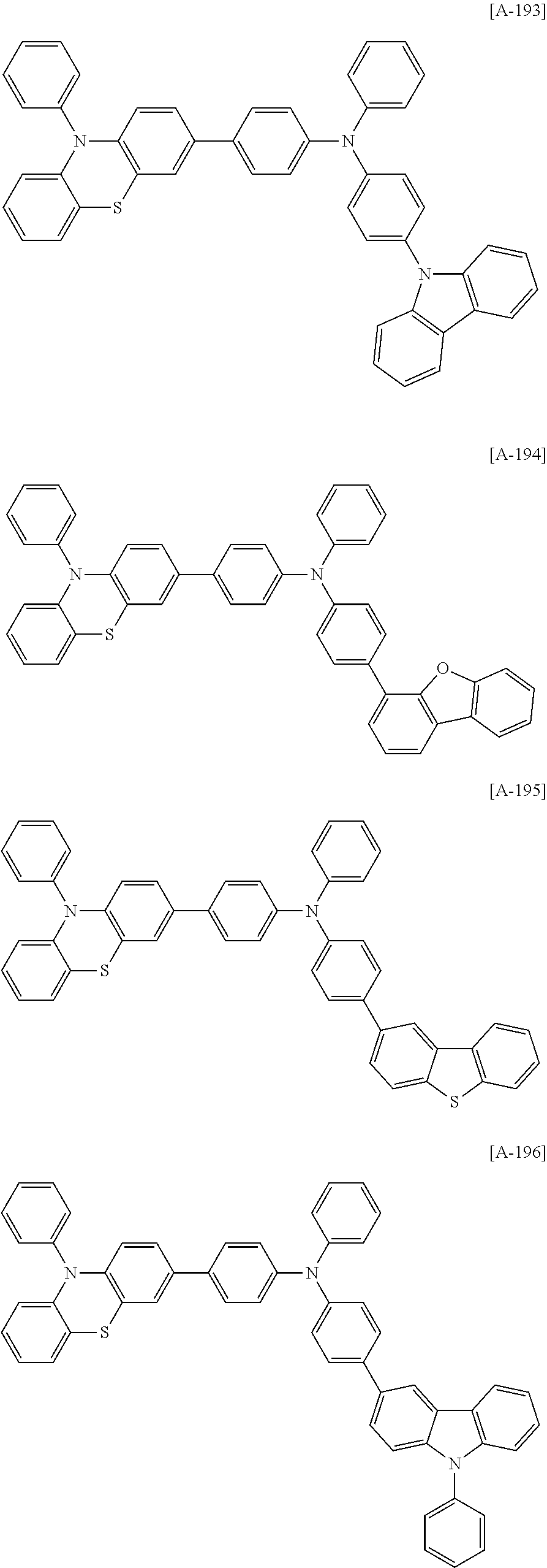


8. The compound for an organic optoelectronic device as claimed in claim 1 , wherein the compound is represented by one of the following Chemical Formulae B-1 to B-81:


9. The compound for an organic optoelectronic device as claimed in claim 1 , wherein the compound is represented by one of the following Chemical Formulae C-1 to C-54.


10. The compound for an organic optoelectronic device as claimed in claim 1 , the compound is represented by one of the following Chemical Formulae D-1 to D-36:


11. The compound for an organic optoelectronic device as claimed in claim 1 , wherein the compound is represented by one of the following Chemical Formulae E-1 to E-18:


12. The compound for an organic optoelectronic device as claimed in claim 1 , wherein the organic optoelectronic device is selected from an organic photoelectric device, an organic light emitting diode, an organic solar cell, an organic transistor, an organic photo-conductor drum, and an organic memory device.
13. An organic light emitting diode, comprising:
an anode, a cathode, and one or more organic thin layers between the anode and the cathode,
wherein at least one of the organic thin layers includes the compound for an organic optoelectronic device as claimed in claim 1 .
14. The organic light emitting diode as claimed in claim 13 , wherein the organic thin layer is selected from an emission layer, a hole transport layer (HTL), a hole injection layer (HIL), an electron transport layer (ETL), an electron injection layer (EIL), a hole blocking layer, and a combination thereof.
15. The organic light emitting diode as claimed in claim 13 , wherein the compound for an organic optoelectronic device is included in a hole transport layer (HTL) or a hole injection layer (HIL).
16. The organic light emitting diode as claimed in claim 13 , wherein the compound for an organic optoelectronic device is included in an emission layer.
17. The organic light emitting diode as claimed in claim 13 , wherein the compound for an organic optoelectronic device is used as a phosphorescent or fluorescent host material in an emission layer.
18. The organic light emitting diode as claimed in claim 13 , wherein the compound for an organic optoelectronic device is used as a fluorescent blue dopant material in an emission layer.
19. A display device comprising the organic light emitting diode as claimed in claim 13 .
Applications Claiming Priority (3)
| Application Number | Priority Date | Filing Date | Title |
|---|---|---|---|
| KR20110035292A KR101486562B1 (en) | 2011-04-15 | 2011-04-15 | Compound For Organic Optoelectronic Device, Organic Light Emitting Diode Including The Same and Display Including The Organic Light Emitting Diode |
| KR10-2011-0035292 | 2011-04-15 | ||
| PCT/KR2011/007312 WO2012141393A1 (en) | 2011-04-15 | 2011-10-04 | Compound for organic optoelectronic device, organic light-emitting diode comprising same, and display device comprising the organic light-emitting diode |
Related Parent Applications (1)
| Application Number | Title | Priority Date | Filing Date |
|---|---|---|---|
| PCT/KR2011/007312 Continuation WO2012141393A1 (en) | 2011-04-15 | 2011-10-04 | Compound for organic optoelectronic device, organic light-emitting diode comprising same, and display device comprising the organic light-emitting diode |
Publications (1)
| Publication Number | Publication Date |
|---|---|
| US20140042412A1 true US20140042412A1 (en) | 2014-02-13 |
Family
ID=47009530
Family Applications (1)
| Application Number | Title | Priority Date | Filing Date |
|---|---|---|---|
| US14/051,737 Abandoned US20140042412A1 (en) | 2011-04-15 | 2013-10-11 | Compound for organic optoelectronic device, organic light-emitting diode including the same and display device including the organic light-emitting diode |
Country Status (3)
| Country | Link |
|---|---|
| US (1) | US20140042412A1 (en) |
| KR (1) | KR101486562B1 (en) |
| WO (1) | WO2012141393A1 (en) |
Cited By (15)
| Publication number | Priority date | Publication date | Assignee | Title |
|---|---|---|---|---|
| US20140155591A1 (en) * | 2012-11-30 | 2014-06-05 | Samsung Display Co., Ltd. | Arylamine compound and electroluminescence device including the same |
| US20140155592A1 (en) * | 2012-11-30 | 2014-06-05 | Samsung Display Co., Ltd. | Arylamine compound and electroluminescence device using the same |
| US20140231774A1 (en) * | 2011-09-09 | 2014-08-21 | Lg Chem, Ltd. | Material for organic light-emitting device, and organic light-emitting device using same |
| US20140284578A1 (en) * | 2013-03-25 | 2014-09-25 | Semiconductor Energy Laboratory Co., Ltd. | Organic Compound, Light-Emitting Element, Light-Emitting Device, Electronic Device, and Lighting Device |
| TWI572595B (en) * | 2014-05-13 | 2017-03-01 | 三星Sdi股份有限公司 | Compound, organic optoelectric device and display device |
| EP3053985A4 (en) * | 2013-09-30 | 2017-05-17 | LG Chem, Ltd. | Heterocyclic compound and organic light-emitting element using same |
| US9812643B2 (en) | 2011-10-27 | 2017-11-07 | Merck Patent Gmbh | Materials for electronic devices |
| US9871203B2 (en) | 2012-02-10 | 2018-01-16 | Idemitsu Kosan Co., Ltd. | Aromatic amine derivative, organic electroluminescent element and electronic device |
| CN108148016A (en) * | 2018-01-22 | 2018-06-12 | 上海升翕光电科技有限公司 | A kind of luminous organic material and preparation method thereof and organic electroluminescence device |
| US20210020854A1 (en) * | 2019-07-17 | 2021-01-21 | Samsung Display Co., Ltd. | Organic electroluminescence device and polycyclic compound for organic electroluminescence device |
| WO2021080334A1 (en) * | 2019-10-23 | 2021-04-29 | 덕산네오룩스 주식회사 | Compound for organic electronic element, organic electronic element using same, and electronic device thereof |
| WO2021088590A1 (en) * | 2019-11-05 | 2021-05-14 | 陕西莱特光电材料股份有限公司 | Nitrogen-containing compound, electronic element and electronic apparatus |
| CN113087675A (en) * | 2021-03-29 | 2021-07-09 | 武汉华星光电半导体显示技术有限公司 | Organic compound, manufacturing method thereof and display panel |
| US11114622B2 (en) * | 2015-10-22 | 2021-09-07 | Samsung Display Co., Ltd. | Compound and organic light-emitting device including the same |
| US11608327B2 (en) | 2016-03-03 | 2023-03-21 | Merck Patent Gmbh | Materials for organic electroluminescent devices |
Families Citing this family (6)
| Publication number | Priority date | Publication date | Assignee | Title |
|---|---|---|---|---|
| KR102261104B1 (en) * | 2012-12-26 | 2021-06-04 | 에스에프씨 주식회사 | An electroluminescent compound and an electroluminescent device comprising the same |
| GB201306365D0 (en) | 2013-04-09 | 2013-05-22 | Kathirgamanathan Poopathy | Heterocyclic compounds and their use in electro-optical or opto-electronic devices |
| KR101664122B1 (en) * | 2013-07-26 | 2016-10-10 | 제일모직 주식회사 | COMPOUND, ORGANIC LiGHT EMITTING DIODE INCLUDING THE SAME, COMPOSITION INCLUDING THE SAME AND DISPLAY INCLUDING THE ORGANIC LiGHT EMITTING DIODE |
| CN103819423B (en) * | 2014-02-13 | 2015-04-15 | 江苏傲伦达科技实业股份有限公司 | Method for synthesizing N-aryl-phenoxazine compounds |
| JP6572682B2 (en) * | 2015-08-28 | 2019-09-11 | 住友化学株式会社 | Compound and light emitting device using the same |
| KR101976662B1 (en) * | 2016-02-18 | 2019-05-09 | 삼성에스디아이 주식회사 | Organic compound and organic optoelectric device and display device |
Family Cites Families (5)
| Publication number | Priority date | Publication date | Assignee | Title |
|---|---|---|---|---|
| JP5112601B2 (en) * | 2003-10-07 | 2013-01-09 | 三井化学株式会社 | Heterocyclic compound and organic electroluminescent device containing the compound |
| US8920942B2 (en) * | 2006-03-23 | 2014-12-30 | Konica Minolta Holdings, Inc. | Organic electroluminescent element, display device and illuminating device |
| JP2009267257A (en) * | 2008-04-28 | 2009-11-12 | Idemitsu Kosan Co Ltd | Material for organic electroluminescent element and organic electroluminescent element using the material |
| KR101324788B1 (en) * | 2009-12-31 | 2013-10-31 | (주)씨에스엘쏠라 | Organic light device and organic light compound for the same |
| JP2011178742A (en) * | 2010-03-03 | 2011-09-15 | Hodogaya Chem Co Ltd | Compound having phenoxazine ring structure or phenothiazine ring structure and organic electroluminescent element |
-
2011
- 2011-04-15 KR KR20110035292A patent/KR101486562B1/en active IP Right Grant
- 2011-10-04 WO PCT/KR2011/007312 patent/WO2012141393A1/en active Application Filing
-
2013
- 2013-10-11 US US14/051,737 patent/US20140042412A1/en not_active Abandoned
Cited By (27)
| Publication number | Priority date | Publication date | Assignee | Title |
|---|---|---|---|---|
| US20140231774A1 (en) * | 2011-09-09 | 2014-08-21 | Lg Chem, Ltd. | Material for organic light-emitting device, and organic light-emitting device using same |
| US9812643B2 (en) | 2011-10-27 | 2017-11-07 | Merck Patent Gmbh | Materials for electronic devices |
| US9871203B2 (en) | 2012-02-10 | 2018-01-16 | Idemitsu Kosan Co., Ltd. | Aromatic amine derivative, organic electroluminescent element and electronic device |
| US20140155591A1 (en) * | 2012-11-30 | 2014-06-05 | Samsung Display Co., Ltd. | Arylamine compound and electroluminescence device including the same |
| US9196841B2 (en) * | 2012-11-30 | 2015-11-24 | Samsung Display Co., Ltd. | Arylamine compound and electroluminescence device using the same |
| US20140155592A1 (en) * | 2012-11-30 | 2014-06-05 | Samsung Display Co., Ltd. | Arylamine compound and electroluminescence device using the same |
| US9496503B2 (en) * | 2013-03-25 | 2016-11-15 | Semiconductor Energy Laboratory Co., Ltd. | Organic compound, light-emitting element, light-emitting device, electronic device, and lighting device |
| US20140284578A1 (en) * | 2013-03-25 | 2014-09-25 | Semiconductor Energy Laboratory Co., Ltd. | Organic Compound, Light-Emitting Element, Light-Emitting Device, Electronic Device, and Lighting Device |
| US10103336B2 (en) | 2013-09-30 | 2018-10-16 | Lg Chem, Ltd. | Heterocyclic compound and organic light-emitting element using same |
| EP3053985A4 (en) * | 2013-09-30 | 2017-05-17 | LG Chem, Ltd. | Heterocyclic compound and organic light-emitting element using same |
| US10326082B2 (en) | 2013-09-30 | 2019-06-18 | Lg Chem, Ltd. | Heterocyclic compound and organic light-emitting element using same |
| US10263193B2 (en) | 2013-09-30 | 2019-04-16 | Lg Chem, Ltd. | Heterocyclic compound and organic light-emitting element using same |
| US10032997B2 (en) | 2013-09-30 | 2018-07-24 | Lg Chem, Ltd. | Heterocyclic compound and organic light-emitting element using same |
| TWI572595B (en) * | 2014-05-13 | 2017-03-01 | 三星Sdi股份有限公司 | Compound, organic optoelectric device and display device |
| US11563179B2 (en) | 2014-05-13 | 2023-01-24 | Samsung Sdi Co., Ltd. | Compound, organic optoelectronic element comprising same and display device thereof |
| JP2017518279A (en) * | 2014-05-13 | 2017-07-06 | サムスン エスディアイ カンパニー, リミテッドSamsung Sdi Co., Ltd. | Compound, organic optoelectronic device including the same, and display |
| US11114622B2 (en) * | 2015-10-22 | 2021-09-07 | Samsung Display Co., Ltd. | Compound and organic light-emitting device including the same |
| US12065431B2 (en) | 2016-03-03 | 2024-08-20 | Merck Patent Gmbh | Materials for organic electroluminescent devices |
| US11608327B2 (en) | 2016-03-03 | 2023-03-21 | Merck Patent Gmbh | Materials for organic electroluminescent devices |
| CN108148016A (en) * | 2018-01-22 | 2018-06-12 | 上海升翕光电科技有限公司 | A kind of luminous organic material and preparation method thereof and organic electroluminescence device |
| US20210020854A1 (en) * | 2019-07-17 | 2021-01-21 | Samsung Display Co., Ltd. | Organic electroluminescence device and polycyclic compound for organic electroluminescence device |
| WO2021080334A1 (en) * | 2019-10-23 | 2021-04-29 | 덕산네오룩스 주식회사 | Compound for organic electronic element, organic electronic element using same, and electronic device thereof |
| US11524970B2 (en) * | 2019-11-05 | 2022-12-13 | Shaanxi Lighte Optoelectronics Material Co., Ltd. | Nitrogen-containing compound, electronic element, and electronic device |
| US20220213124A1 (en) * | 2019-11-05 | 2022-07-07 | Shaanxi Lighte Optoelectronics Material Co., Ltd. | Nitrogen-containing compound, electronic element, and electronic device |
| WO2021088590A1 (en) * | 2019-11-05 | 2021-05-14 | 陕西莱特光电材料股份有限公司 | Nitrogen-containing compound, electronic element and electronic apparatus |
| WO2022205587A1 (en) * | 2021-03-29 | 2022-10-06 | 武汉华星光电半导体显示技术有限公司 | Organic compound and production method therefor, and display panel |
| CN113087675A (en) * | 2021-03-29 | 2021-07-09 | 武汉华星光电半导体显示技术有限公司 | Organic compound, manufacturing method thereof and display panel |
Also Published As
| Publication number | Publication date |
|---|---|
| WO2012141393A1 (en) | 2012-10-18 |
| KR101486562B1 (en) | 2015-01-28 |
| KR20120117501A (en) | 2012-10-24 |
| WO2012141393A9 (en) | 2013-10-31 |
Similar Documents
| Publication | Publication Date | Title |
|---|---|---|
| US20140042412A1 (en) | Compound for organic optoelectronic device, organic light-emitting diode including the same and display device including the organic light-emitting diode | |
| US10121973B2 (en) | Compound for organic optoelectronic device, organic light-emitting diode including same, and display device including organic light-emitting diode | |
| US20230209997A1 (en) | Organic alloy for organic optoelectronic device, organic optoelectronic device, and display device | |
| US9246107B2 (en) | Compound for organic optoelectronic device, organic light emitting diode including the same and display device including the organic light emitting diode | |
| US8993783B2 (en) | Compound for organic photoelectric device and organic photoelectric device including the same | |
| US9478753B2 (en) | Compound for organic optoelectronic device, organic light emitting diode including the same, and display device including the light emitting diode | |
| US8890126B2 (en) | Compound for optoelectronic device, organic light emitting diode including the same, and display including the organic light emitting diode | |
| US9559309B2 (en) | Compound for organic optoelectronic device, organic light emitting diode including the same, and display device including the organic light emitting diode | |
| US9450193B2 (en) | Compound for organic photoelectric device and organic photoelectric device including the same | |
| US9136481B2 (en) | Compound for an organic photoelectric device, organic photoelectric device including the same, and display device including the organic photoelectric device | |
| US10680182B2 (en) | Fluoranthene compound, and organic electronic device comprising same | |
| US20150263294A1 (en) | Compound for organic optoelectronic device, organic light-emitting device including same, and display device including the organic light- emitting diode | |
| US10381571B2 (en) | Compound, organic light emitting element comprising same, and display device comprising organic light emitting element | |
| US20150280136A1 (en) | Organic optoelectronic device, and display device including the same | |
| US10193081B2 (en) | Organic compound for optoelectric device and composition for optoelectric device and organic optoelectric device and display device | |
| KR101453768B1 (en) | Compound for organic photoelectric device and organic photoelectric device including the same | |
| US9502662B2 (en) | Compound for an organic optoelectronic device, organic light-emitting element comprising same, and display device comprising the organic light-emitting element | |
| US9899607B2 (en) | Compound for organic optoelectronic device, organic light emitting diode including the same and display including the organic light emitting diode | |
| US20130207092A1 (en) | Compound for organic photoelectric device and organic photoelectric device including the same | |
| US9793488B2 (en) | Compound for organic optoelectronic element, organic light-emitting element comprising same, and display device comprising the organic light-emitting element | |
| US9444054B2 (en) | Compound for organic optoelectronic device and organic light emitting diode including the same | |
| KR101638665B1 (en) | New compound and organic light emitting device using the same | |
| US20230200234A1 (en) | Organic compound, and electronic component and electronic device therefor | |
| US20150021563A1 (en) | Compound for organic optoelectronic device, organic light emitting diode including the same and display including the organic light emitting diode | |
| US9825242B2 (en) | Compound for organic optoelectric device, organic light-emitting diode including same, display device including organic light-emitting diode |
Legal Events
| Date | Code | Title | Description |
|---|---|---|---|
| AS | Assignment |
Owner name: CHEIL INDUSTRIES, INC., KOREA, REPUBLIC OF Free format text: ASSIGNMENT OF ASSIGNORS INTEREST;ASSIGNORS:RYU, DONG-WAN;JUNG, SUNG-HYUN;HUH, DAL-HO;AND OTHERS;REEL/FRAME:031388/0439 Effective date: 20130925 |
|
| STCB | Information on status: application discontinuation |
Free format text: EXPRESSLY ABANDONED -- DURING EXAMINATION |