US20090213253A1 - Solid-state imaging apparatus - Google Patents
Solid-state imaging apparatus Download PDFInfo
- Publication number
- US20090213253A1 US20090213253A1 US12/391,448 US39144809A US2009213253A1 US 20090213253 A1 US20090213253 A1 US 20090213253A1 US 39144809 A US39144809 A US 39144809A US 2009213253 A1 US2009213253 A1 US 2009213253A1
- Authority
- US
- United States
- Prior art keywords
- pixel
- section
- signal
- pixels
- electric potential
- Prior art date
- Legal status (The legal status is an assumption and is not a legal conclusion. Google has not performed a legal analysis and makes no representation as to the accuracy of the status listed.)
- Granted
Links
Images






Classifications
-
- H—ELECTRICITY
- H04—ELECTRIC COMMUNICATION TECHNIQUE
- H04N—PICTORIAL COMMUNICATION, e.g. TELEVISION
- H04N25/00—Circuitry of solid-state image sensors [SSIS]; Control thereof
- H04N25/70—SSIS architectures; Circuits associated therewith
- H04N25/76—Addressed sensors, e.g. MOS or CMOS sensors
-
- H—ELECTRICITY
- H04—ELECTRIC COMMUNICATION TECHNIQUE
- H04N—PICTORIAL COMMUNICATION, e.g. TELEVISION
- H04N25/00—Circuitry of solid-state image sensors [SSIS]; Control thereof
- H04N25/60—Noise processing, e.g. detecting, correcting, reducing or removing noise
- H04N25/62—Detection or reduction of noise due to excess charges produced by the exposure, e.g. smear, blooming, ghost image, crosstalk or leakage between pixels
- H04N25/628—Detection or reduction of noise due to excess charges produced by the exposure, e.g. smear, blooming, ghost image, crosstalk or leakage between pixels for reducing horizontal stripes caused by saturated regions of CMOS sensors
Definitions
- the present invention relates to solid-state imaging apparatus for use for example in a video camera, digital still camera, etc., and more particularly relates to the solid-state imaging apparatus using an amplified solid-state imaging device having an amplification function within its imaging region.
- MOS Metal Oxide Semiconductor
- image sensor image sensor
- CCD Charge Coupled Device
- MOS image sensors have an identical manufacturing process as other LSI's and thus are superior in providing many functions as they are readily made into an SOC (system on chip).
- MOS image sensors have an amplification circuit (amplifier) in each individual pixel to amplify signal electric charges within the pixel, they are less likely to be affected by noise due to the transmission path of signals.
- the signal electric charges in each pixel of the MOS image sensor can be extracted by means of a selection system so that in theory, the accumulation time and/or read sequence of signals can be arbitrarily controlled pixel by pixel.
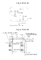
- FIG. 1 schematically illustrates an image in the case with an occurrence of the transverse stripe phenomenon at the time of incidence of high-luminance light. Shown in FIG.
- FIG. 2 shows a block diagram of a typical MOS image sensor. Pixels for converting light into electrical signal are two-dimensionally arranged into a matrix, where P(i, j) represents a unit pixel of i′ th row and j′ th column (i, j: an integral number). The pixel P(i, j) is to output a received light as voltage onto a vertical signal line SL-V(j) by means of a reset pulse ⁇ RS(i), a transfer pulse ⁇ TX(i), and a select pulse ⁇ SE(i) outputted from a vertical scanning circuit 101 .
- the pixel P(i, j) is connected to a constant current supply CCS(j) and to a CDS (Correlated Double Sampling) circuit CDS(j) through the vertical signal line SL-V(j).
- the CDS circuit CDS(j) is connected to a horizontal signal line SL-H through the vertical signal line SL-V(j).
- the CDS circuit CDS(j) eliminates variance of signal that is different from one pixel to another by differentiating between a reset signal and an image signal from the pixel (i, j) by means of a clamp pulse ⁇ CL and a sample-and-hold pulse ⁇ SH.
- An output from the CDS circuit CDS(j) is outputted onto the horizontal signal line SL-H by means of a column select pulse ⁇ HP outputted from the horizontal scanning circuit 102 so as to obtain a signal Vout amplified at an amplification circuit Amp.
- a column select pulse ⁇ HP outputted from the horizontal scanning circuit 102 so as to obtain a signal Vout amplified at an amplification circuit Amp.
- FIG. 3 shows a circuit diagram of the pixel P(i, j) and the constant current supply CCS(j) in FIG. 2 .
- a unit pixel P(i, j) includes: PD(i, j), a photodiode; Mtr(i, j), a transfer transistor; Msf(i, j), an amplification transistor; Mrs(i, j), a reset transistor; Mse(i, j), a select transistor; FD(i, j), a floating diffusion section; SL-V(j), a vertical signal line; Vgs(i, j), a gate-source voltage of the amplification transistor Msf(i, j); CCS(j), a constant current supply; Vccsgs(j), a gate-source voltage of the transistor of the constant current supply CCS(j); Vsl-v(j), a voltage of vertical signal line; SL-V(j), a vertical signal line; Vdd, a power supply
- FIG. 4 is a circuit diagram of the CDS circuit CDS(j) in FIG. 2 .
- FIG. 4 includes: Mcl(j), a clamp transistor; Msh(j), a sample-and-hold transistor; Ccl(j), a clamp capacitor; Csh(j), a sample-and-hold capacitor; Vcdso(i, j), an output voltage from the CDS circuit CDS(j); Vcl, a clamp voltage; ⁇ CL, a clamp pulse; and ⁇ SH, a sample-and-hold pulse.
- a clip circuit for example to clip voltage of the vertical signal line is separately provided to clip the vertical signal line by a predetermined voltage in the period of reading signal of light so that the voltage of the vertical signal line is controlled so as not to depart from an operation range of the current supply.
- a solid-state imaging apparatus including: a pixel section having a plurality of pixels two-dimensionally arranged into a matrix, each pixel containing a photoelectric conversion section for converting an incident light into signal electric charges, an accumulation section for accumulating the signal electric charges, a transfer section for transferring the signal electric charges to the accumulation section, an amplification section for amplifying and outputting as pixel signal the signal electric charges accumulated at the accumulation section, and a reset section for resetting the accumulation section by supplying an electric potential retained on a power supply line to the accumulation section, the pixel section having output signal lines provided column by column onto which the pixel signal is outputted, connected to the other end of a constant current supply having one end grounded; and a control section where, of a first one of the pixels and a second one of the pixels connected to the same one output signal line, taking the first pixel as one of the pixels subject to reading of pixel signal conforming to the incident light and the second pixel as non-subject one
- control section in the solid-state imaging apparatus sets the second pixel near to the first pixel.
- control section in the solid-state imaging apparatus causes an output when driving the reset section within the second pixel to be outputted from the second pixel onto the output signal line.
- the electric potential of the power supply line of the pixel in the pixel section in the solid-state imaging apparatus according-to the third aspect is changeable row by row by the control section, and the control section respectively sets a first electric potential corresponding to reading of pixel signal conforming to the incident light to the power supply line associated with the first pixel and a second electric potential corresponding to keeping and control of operation for the constant current supply to the power supply line associated with the second pixel.
- control section in the solid-state imaging apparatus causes an end timing of outputting from the second pixel onto the output signal line to be delayed from an end timing of outputting of the pixel signal from the first pixel onto the output signal line.
- the pixel section in the solid-state imaging apparatus is formed such that the power supply lines of all pixels are connected in common to a single power supply of which the electric potential is changeable by the control section, and the control section, taking a timing for driving the reset section within the second pixel as a first timing, drives the reset section of the first pixel by a second timing different from the first timing, and respectively changes the electric potential of the power supply at the first timing to a second electric potential corresponding to keeping and control of operation for the constant current supply and at the second timing to a first electric potential corresponding to reading of pixel signal conforming to the incident light.
- control section in the solid-state imaging apparatus maintains the electric potential of the power supply line of the second pixel to an electric potential corresponding to keeping and control of operation for the constant current supply and causes the reset section to remain in its driven state even after the outputting of the pixel signal from the first pixel onto the output signal line.
- FIG. 1 illustrates a manner of occurrence of the transverse stripe phenomenon when a high-luminance light is incident in the vicinity of a center of an image sensor.
- FIG. 2 is a block diagram schematically showing construction of a prior-art MOS image sensor.
- FIG. 3 is a circuit diagram showing construction of pixel in the MOS image sensor shown in FIG. 2 .
- FIG. 4 is a circuit diagram showing construction of a CDS circuit in the MOS image sensor shown in FIG. 2 .
- FIG. 5 illustrates operation when a high-luminance light enters the MOS image sensor shown in FIG. 2 .
- FIG. 6 is a block diagram schematically showing construction of a first embodiment of the solid-state imaging apparatus according to the invention.
- FIG. 7 is a circuit diagram showing construction of pixel in the first embodiment shown in FIG. 6 .
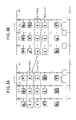
- FIGS. 8A and 8B illustrate the manner where the clip voltage generating pixel row is moved in accordance with movement of the signal reading pixel row.
- FIG. 9 shows the manner where the pixel power supply Vdd(i) is driven so as to cause an independent change row by row in the first embodiment shown in FIG. 6 .
- FIG. 10 is a timing chart for explaining read operation of pixel signal in the first embodiment shown in FIG. 6 .
- FIG. 11 is a partially omitted block diagram showing construction of a second embodiment of the solid-state imaging apparatus according to the invention.
- FIG. 12 is a circuit diagram showing construction of pixel in the second embodiment shown in FIG. 11 .
- FIG. 13 is a timing chart for explaining operation of the second embodiment shown in FIG. 11 .
- the present invention is to suppress an occurrence of the transverse stripe phenomenon at the time of incidence of high-luminance light with using an output of pixel of the pixel section without providing a separate clip circuit.
- variance in the suppressing operation is controlled by using the fact that the gate-source voltages of amplification transistor of pixels proximate to each other do take near values due to the manufacturing process.
- a pixel for generating clip voltage is selected so that it is always proximate to the pixel from which signal of light is read out, thereby generating a clip voltage for preventing the transverse stripe phenomenon at the time of incidence of high luminance light with using the fact that the gate-source voltages of the respective amplification transistors of the two pixels take near (substantially the same) values.
- a clip voltage generating pixel is set in the vicinity of a pixel for reading signal, and in accordance with movement of the pixel (row) to be read, the clip voltage generating pixel (row) connected to the same one vertical signal line SL-V(j) is also correspondingly moved.
- the values of the respective gate-source voltages Vgs of the amplification transistors in the clip voltage generating pixel and the pixel for reading signal of light are thereby made near to each other throughout the reading of light signals of all pixels.
- FIG. 6 is a block diagram of the MOS solid-state imaging apparatus according to the first embodiment, where like or corresponding components as in the prior-art example shown in FIG. 2 are denoted by like symbols, and a description thereof will be partially omitted.
- pixels P(i, j)(i, j being an integral number) are arranged into a two-dimensional array; it is different from the prior-art example shown in FIG. 2 in that the pixel power supply Vdd(i) to each pixel is made variable row by row, and the construction of the rest is identical as the prior-art example shown in FIG. 2 .
- the construction of CDS circuit CDS(j) is also identical to that in the prior-art example shown in FIG. 4 .
- FIG. 7 is a circuit diagram showing construction of a pixel P(i, j) in FIG. 6 ; it is of the same construction as the prior-art example shown in FIG. 3 except that the pixel power supply Vdd(i) is made variable row by row.
- FIGS. 8A and 8B typically illustrate the manner in which the clip voltage generating pixel is moved in accordance with movement of the pixel for reading signal.
- pixels of the third pixel row are the pixels for reading light signal
- pixels of the second pixel row connected to the same one vertical signal line SL-V(j) are the pixels for generating clip voltage.
- FIG. 8B shows the manner in which the signal reading pixel row has moved to the fourth row, and as a result of such moving, the clip voltage generating pixel row has been moved to the third row connected to the same one vertical signal line SL-V(j).
- the respective gate-source voltages Vgs of each amplification transistor of the light signal reading pixel and the clip voltage generating pixel are to take near values to each other.
- those pixels after ending light signal readout are used to generate clip voltage.
- FIG. 9 is a partially omitted block diagram showing the manner of driving the pixel power supply Vdd(i) in the first embodiment so that it is changed independently for each row, where a pixel power supply Vdd(i) is applied on the signal reading pixel row of the i′ th row, and where a pixel power supply Vdd(i-1) different from the pixel power supply Vdd(i) is applied on the clip voltage generating pixel row of the (i-1)′ th row.
- a power supply voltage Vdd is applied as pixel power supply Vdd(i) at the signal read pixel P(i, j), and a voltage (Vdd ⁇ Va) lower by Va than the power supply voltage Vdd is applied as pixel power supply Vdd(i-1) at the clip voltage generating pixel P(i-1, j).
- Vgs( 1 ) is the gate-source voltage of the amplification transistor of the signal read pixel P(i, j).
- both the clamp pulse ⁇ CL and the sample-and-hold pulse ⁇ SH of the CDS circuit are also at H level.
- the select pulse ⁇ SE(i) is brought to L level at the signal read pixel P(i, j) and the select pulse ⁇ SE(i-1) and the reset pulse ⁇ RS(i-1) to L level at the clip voltage generating pixel (i-1, j), and at the same time the sample-and-hold pulse ⁇ SH of the CDS circuit is brought to L level so as to effect processing by the CDS circuit.
- the timing that the select pulse ⁇ SE(i-1) is brought to L level is somewhat delayed from the time t 3 .
- Vgs( 1 ) is a gate-source voltage of the amplification transistor of the signal read pixel
- Vgs( 2 ) is a gate-source voltage of the amplification transistor of the clip voltage generating pixel
- Vrs( 1 ) is a reset level of the pixel to be read
- the clip voltage Vclip is a voltage at which the current supply CCS(j) does not enter its non-saturation region
- Vrs-sig is a signal output.
- Verr>0 clip operation is effective.
- the threshold to clip therefore, does not depend on the gate-source voltage of the amplification transistor.
- FIG. 11 is a block diagram showing in a partially omitted manner construction of the solid-state imaging apparatus according to the second embodiment.
- a pixel row of i′ th row is supposed as the pixel row for reading signal, a pixel row of (i-1)′ th row as the pixel row for generating clip voltage, and a pixel row of (i-2)′ th row as pixel row not to be read.
- FIG. 12 is a circuit diagram showing a pixel construction of unit pixel of the pixel section shown in FIG.
- each unit pixel is not provided with a select transistor as that in the pixel of the first embodiment but includes: a photodiode PD(i, j); a floating diffusion section FD(i, j); a transfer transistor Mtr(i, j); an amplification transistor Msf(i, j); and a reset transistor Mrs(i, j).
- One end of the amplification transistor of each pixel arranged in a column direction is respectively connected in common to a vertical signal line SL-V(j).
- a pixel power supply ⁇ Vdd to the power supply line connected in common to each pixel then is driven in a manner of pulse to 3 electric potentials, i.e. a power supply voltage Vdd, a clip voltage (Vdd ⁇ Va), and a voltage (Vdd ⁇ Va ⁇ Vb) lower than the clip voltage.
- the construction of the rest is similar to the first embodiment.
- FIG. 13 is a timing chart for explaining operation of the solid-state imaging apparatus according to the second embodiment having the above construction.
- the operation of this embodiment is different from the operation of the first embodiment only in the following operation based on the fact that the pixel is formed as having 3-transistor construction and the pixel power supply ⁇ Vdd is driven in a manner of pulse to 3 electric potentials.
- the pixel power supply ⁇ Vdd to the pixel row to become a non-read pixel row [(i-2)′ th row] is set to a voltage (Vdd ⁇ Va ⁇ Vb) that is lower than the clip voltage (Vdd ⁇ Va) so as not to output a pixel output of the non-read pixel row onto the vertical signal line SL-V(j) so that the signal readout of the row to be read is not affected.
- the output of a second pixel connected to the same one output signal line as the first pixel is used so that a constant current supply connected to one end of the output signal line is kept in its operable range. It is thereby possible to achieve a solid-state imaging apparatus capable of effectively suppressing the transverse stripe phenomenon at the time of incidence of high-luminance light with controlling variance without providing a separate clip circuit.
Landscapes
- Engineering & Computer Science (AREA)
- Multimedia (AREA)
- Signal Processing (AREA)
- Transforming Light Signals Into Electric Signals (AREA)
- Solid State Image Pick-Up Elements (AREA)
Abstract
Description
- This application claims benefit of Japanese Patent Application No. 2008-43969 filed in Japan Feb. 26, 2008, the contents of which are incorporated by this reference.
- The present invention relates to solid-state imaging apparatus for use for example in a video camera, digital still camera, etc., and more particularly relates to the solid-state imaging apparatus using an amplified solid-state imaging device having an amplification function within its imaging region.
- In recent years, MOS (Metal Oxide Semiconductor) type imaging devices (image sensor) are drawing attention and are practically used as solid-state imaging device. The MOS imaging devices are capable of being driven by a single power supply as compared to CCD (Charge Coupled Device) type imaging devices. Further, while CCD imaging devices require an exclusive process, the MOS image sensors have an identical manufacturing process as other LSI's and thus are superior in providing many functions as they are readily made into an SOC (system on chip). Furthermore, since the MOS image sensors have an amplification circuit (amplifier) in each individual pixel to amplify signal electric charges within the pixel, they are less likely to be affected by noise due to the transmission path of signals. Moreover, the signal electric charges in each pixel of the MOS image sensor can be extracted by means of a selection system so that in theory, the accumulation time and/or read sequence of signals can be arbitrarily controlled pixel by pixel.
- With the MOS image sensors, when a high-luminance light is incident on a partial region, a change in electric potential occurs along a left and right direction of the rows on which the high-luminance light is incident so that an image as if a white band-like light is incident is obtained. Such a phenomenon in the present specification will be referred to hereinafter as “transverse stripe phenomenon” at the time of incidence of high-luminance light.
FIG. 1 schematically illustrates an image in the case with an occurrence of the transverse stripe phenomenon at the time of incidence of high-luminance light. Shown inFIG. 1 is an output image when the high-luminance light is incident in the vicinity of a center of the image sensor, where a band-like transverse stripe due to change in electric potential is seen along the row direction on the left and right thereof. This transverse stripe phenomenon at the time of incidence of high-luminance light will be described below together with a typical operation of MOS image sensor. -
FIG. 2 shows a block diagram of a typical MOS image sensor. Pixels for converting light into electrical signal are two-dimensionally arranged into a matrix, where P(i, j) represents a unit pixel of i′ th row and j′ th column (i, j: an integral number). The pixel P(i, j) is to output a received light as voltage onto a vertical signal line SL-V(j) by means of a reset pulse φ RS(i), a transfer pulse φ TX(i), and a select pulse φ SE(i) outputted from avertical scanning circuit 101. The pixel P(i, j) is connected to a constant current supply CCS(j) and to a CDS (Correlated Double Sampling) circuit CDS(j) through the vertical signal line SL-V(j). The CDS circuit CDS(j) is connected to a horizontal signal line SL-H through the vertical signal line SL-V(j). The CDS circuit CDS(j) eliminates variance of signal that is different from one pixel to another by differentiating between a reset signal and an image signal from the pixel (i, j) by means of a clamp pulse φ CL and a sample-and-hold pulse φ SH. An output from the CDS circuit CDS(j) is outputted onto the horizontal signal line SL-H by means of a column select pulse φ HP outputted from thehorizontal scanning circuit 102 so as to obtain a signal Vout amplified at an amplification circuit Amp. By repeating the above operation for a predetermined number of pixels, two-dimensional image signals can be obtained. These operations are controlled by signals outputted from thevertical scanning circuit 101 and thehorizontal scanning circuit 102 under instructions from a controlsignal generation circuit 103. -
FIG. 3 shows a circuit diagram of the pixel P(i, j) and the constant current supply CCS(j) inFIG. 2 . A unit pixel P(i, j) includes: PD(i, j), a photodiode; Mtr(i, j), a transfer transistor; Msf(i, j), an amplification transistor; Mrs(i, j), a reset transistor; Mse(i, j), a select transistor; FD(i, j), a floating diffusion section; SL-V(j), a vertical signal line; Vgs(i, j), a gate-source voltage of the amplification transistor Msf(i, j); CCS(j), a constant current supply; Vccsgs(j), a gate-source voltage of the transistor of the constant current supply CCS(j); Vsl-v(j), a voltage of vertical signal line; SL-V(j), a vertical signal line; Vdd, a power supply voltage line; Vccsg, a gate voltage line of the transistor within the constant current supply CCS(j). -
FIG. 4 is a circuit diagram of the CDS circuit CDS(j) inFIG. 2 .FIG. 4 includes: Mcl(j), a clamp transistor; Msh(j), a sample-and-hold transistor; Ccl(j), a clamp capacitor; Csh(j), a sample-and-hold capacitor; Vcdso(i, j), an output voltage from the CDS circuit CDS(j); Vcl, a clamp voltage; φ CL, a clamp pulse; and φ SH, a sample-and-hold pulse. At the CDS circuit CDS(j), a reset signal (voltage at the time of attaining φ CL=Low) and a signal of light (voltage at the time of attaining φ SH=Low) of pixel in the column j are differentiated so as to output Vcdso(i, j). - An operation in the case where a high-luminance light is incident in the MOS image sensor having such construction will now be described by way of
FIG. 5 . - (1): when a light having a large light amount has entered the pixel (i, j), the electrical potential of the vertical signal line SL-V(j) at the time of outputting an image signal of the pixel (i, j) is extremely lowered so that a voltage outside of an operation range of the current supply CCS(j) (voltage in a non-saturation region of the drain-source voltage Vccsds of the transistor of the current supply CCS(j)) is applied on the current supply CCS(j).
- (2): as a result that the condition of (1) has been attained, the current supply CCS(j) is caused to operate in its non-saturation region so that the electric current becomes smaller than normal.
- (3): as a result that the condition of (2) has been attained, a total sum of the currents following through a ground line GL-H connected to each current supply is also reduced. A voltage drop due to wiring resistance Rgl-h(j+k) on the ground line connected to the current supply CCS(j) is thereby reduced so that the gate-source voltage Vccsgs of the transistor within the current supply CCS(j+k) becomes larger.
- (4): as a result that the condition of (3) has been attained, i.e. due to the fact that the gate-source voltage Vccsgs of the transistor within the current supply CCS(j+k) is increased, a current greater than normal is caused to flow through the vertical signal line SL-V(j+k) connected to the pixel P(i, j+k) on which the high-luminance light is not incident.
- (5): as a result that the condition of (4) has been attained, when the current is increased, the gate-source voltage Vgs of the amplification transistor within the pixel P(i, j+k) also becomes greater than that at the time of incidence of normal light, and as a result, the value of signal becomes greater than normal (lighter as an image).
- Accordingly, a dark region reflected as black on the image when condition is normal or a region on the left and right of the region on which the high-luminance light is incident is reflected on the image inevitably in a lighter-than-black condition when the high-luminance light is incident. As a result, a lighter band-like transverse stripe is observed along a row direction on the left and right of where the high-luminance light is incident.
- As a measure to avoid this transverse stripe phenomenon occurring at the time of incidence of high-luminance light, one constructed as in the following has been proposed for example in Japanese Patent Application Laid-Open 2001-230974. Specifically in the proposed construction, a clip circuit for example to clip voltage of the vertical signal line is separately provided to clip the vertical signal line by a predetermined voltage in the period of reading signal of light so that the voltage of the vertical signal line is controlled so as not to depart from an operation range of the current supply.
- In a first aspect of the invention, there is provided a solid-state imaging apparatus including: a pixel section having a plurality of pixels two-dimensionally arranged into a matrix, each pixel containing a photoelectric conversion section for converting an incident light into signal electric charges, an accumulation section for accumulating the signal electric charges, a transfer section for transferring the signal electric charges to the accumulation section, an amplification section for amplifying and outputting as pixel signal the signal electric charges accumulated at the accumulation section, and a reset section for resetting the accumulation section by supplying an electric potential retained on a power supply line to the accumulation section, the pixel section having output signal lines provided column by column onto which the pixel signal is outputted, connected to the other end of a constant current supply having one end grounded; and a control section where, of a first one of the pixels and a second one of the pixels connected to the same one output signal line, taking the first pixel as one of the pixels subject to reading of pixel signal conforming to the incident light and the second pixel as non-subject one of the pixels set in accordance with a location of the first pixel, an output from the second pixel onto the output signal line is used at the time of outputting of the pixel signal from the first pixel onto the output signal line to effect control so that an electric potential difference between the one end and the other end of the constant current supply is kept in a range where the constant current supply is operable.
- In a second aspect of the invention, the control section in the solid-state imaging apparatus according to the first aspect sets the second pixel near to the first pixel.
- In a third aspect of the invention, the control section in the solid-state imaging apparatus according to the first aspect causes an output when driving the reset section within the second pixel to be outputted from the second pixel onto the output signal line.
- In a fourth aspect of the invention, the electric potential of the power supply line of the pixel in the pixel section in the solid-state imaging apparatus according-to the third aspect is changeable row by row by the control section, and the control section respectively sets a first electric potential corresponding to reading of pixel signal conforming to the incident light to the power supply line associated with the first pixel and a second electric potential corresponding to keeping and control of operation for the constant current supply to the power supply line associated with the second pixel.
- In a fifth aspect of the invention, the control section in the solid-state imaging apparatus according to the first aspect causes an end timing of outputting from the second pixel onto the output signal line to be delayed from an end timing of outputting of the pixel signal from the first pixel onto the output signal line.
- In a sixth aspect of the invention, the pixel section in the solid-state imaging apparatus according to the third aspect is formed such that the power supply lines of all pixels are connected in common to a single power supply of which the electric potential is changeable by the control section, and the control section, taking a timing for driving the reset section within the second pixel as a first timing, drives the reset section of the first pixel by a second timing different from the first timing, and respectively changes the electric potential of the power supply at the first timing to a second electric potential corresponding to keeping and control of operation for the constant current supply and at the second timing to a first electric potential corresponding to reading of pixel signal conforming to the incident light.
- In a seventh aspect of the invention, the control section in the solid-state imaging apparatus according to the fourth aspect maintains the electric potential of the power supply line of the second pixel to an electric potential corresponding to keeping and control of operation for the constant current supply and causes the reset section to remain in its driven state even after the outputting of the pixel signal from the first pixel onto the output signal line.
-
FIG. 1 illustrates a manner of occurrence of the transverse stripe phenomenon when a high-luminance light is incident in the vicinity of a center of an image sensor. -
FIG. 2 is a block diagram schematically showing construction of a prior-art MOS image sensor. -
FIG. 3 is a circuit diagram showing construction of pixel in the MOS image sensor shown inFIG. 2 . -
FIG. 4 is a circuit diagram showing construction of a CDS circuit in the MOS image sensor shown inFIG. 2 . -
FIG. 5 illustrates operation when a high-luminance light enters the MOS image sensor shown inFIG. 2 . -
FIG. 6 is a block diagram schematically showing construction of a first embodiment of the solid-state imaging apparatus according to the invention. -
FIG. 7 is a circuit diagram showing construction of pixel in the first embodiment shown inFIG. 6 . -
FIGS. 8A and 8B illustrate the manner where the clip voltage generating pixel row is moved in accordance with movement of the signal reading pixel row. -
FIG. 9 shows the manner where the pixel power supply Vdd(i) is driven so as to cause an independent change row by row in the first embodiment shown inFIG. 6 . -
FIG. 10 is a timing chart for explaining read operation of pixel signal in the first embodiment shown inFIG. 6 . -
FIG. 11 is a partially omitted block diagram showing construction of a second embodiment of the solid-state imaging apparatus according to the invention. -
FIG. 12 is a circuit diagram showing construction of pixel in the second embodiment shown inFIG. 11 . -
FIG. 13 is a timing chart for explaining operation of the second embodiment shown inFIG. 11 . - Some embodiments of the solid-state imaging apparatus according to the present invention will be described below with reference to the drawings.
- The present invention is to suppress an occurrence of the transverse stripe phenomenon at the time of incidence of high-luminance light with using an output of pixel of the pixel section without providing a separate clip circuit. Specifically, variance in the suppressing operation is controlled by using the fact that the gate-source voltages of amplification transistor of pixels proximate to each other do take near values due to the manufacturing process. In particular, a pixel for generating clip voltage is selected so that it is always proximate to the pixel from which signal of light is read out, thereby generating a clip voltage for preventing the transverse stripe phenomenon at the time of incidence of high luminance light with using the fact that the gate-source voltages of the respective amplification transistors of the two pixels take near (substantially the same) values.
- A specific first embodiment will now be described. In the first embodiment, a clip voltage generating pixel is set in the vicinity of a pixel for reading signal, and in accordance with movement of the pixel (row) to be read, the clip voltage generating pixel (row) connected to the same one vertical signal line SL-V(j) is also correspondingly moved. The values of the respective gate-source voltages Vgs of the amplification transistors in the clip voltage generating pixel and the pixel for reading signal of light are thereby made near to each other throughout the reading of light signals of all pixels.
-
FIG. 6 is a block diagram of the MOS solid-state imaging apparatus according to the first embodiment, where like or corresponding components as in the prior-art example shown inFIG. 2 are denoted by like symbols, and a description thereof will be partially omitted. Also in the first embodiment, pixels P(i, j)(i, j being an integral number) are arranged into a two-dimensional array; it is different from the prior-art example shown inFIG. 2 in that the pixel power supply Vdd(i) to each pixel is made variable row by row, and the construction of the rest is identical as the prior-art example shown inFIG. 2 . The construction of CDS circuit CDS(j) is also identical to that in the prior-art example shown inFIG. 4 .FIG. 7 is a circuit diagram showing construction of a pixel P(i, j) inFIG. 6 ; it is of the same construction as the prior-art example shown inFIG. 3 except that the pixel power supply Vdd(i) is made variable row by row. -
FIGS. 8A and 8B typically illustrate the manner in which the clip voltage generating pixel is moved in accordance with movement of the pixel for reading signal. InFIG. 8A , pixels of the third pixel row are the pixels for reading light signal, and pixels of the second pixel row connected to the same one vertical signal line SL-V(j) are the pixels for generating clip voltage.FIG. 8B shows the manner in which the signal reading pixel row has moved to the fourth row, and as a result of such moving, the clip voltage generating pixel row has been moved to the third row connected to the same one vertical signal line SL-V(j). By moving the clip voltage generating pixel in this manner so that it comes near to the signal reading pixel, the respective gate-source voltages Vgs of each amplification transistor of the light signal reading pixel and the clip voltage generating pixel are to take near values to each other. In the construction shown inFIGS. 8A and 8B , those pixels after ending light signal readout are used to generate clip voltage. -
FIG. 9 is a partially omitted block diagram showing the manner of driving the pixel power supply Vdd(i) in the first embodiment so that it is changed independently for each row, where a pixel power supply Vdd(i) is applied on the signal reading pixel row of the i′ th row, and where a pixel power supply Vdd(i-1) different from the pixel power supply Vdd(i) is applied on the clip voltage generating pixel row of the (i-1)′ th row. - A read operation of the pixel signals will now be described by way of a timing chart shown in
FIG. 10 . First, a power supply voltage Vdd is applied as pixel power supply Vdd(i) at the signal read pixel P(i, j), and a voltage (Vdd−Va) lower by Va than the power supply voltage Vdd is applied as pixel power supply Vdd(i-1) at the clip voltage generating pixel P(i-1, j). At time t1, when the select pulse φ SE(i) and the reset pulse φ RS(i) for the signal read pixel P(i, j) are driven to H level, voltage Vfd(i, j) of the floating diffusion section is fixed to the power supply voltage Vdd. The voltage Vsl-v(j) on the vertical signal line SL-V(j) thereby attains Vrs(1)[=Vdd−Vgs(1)]. Here, Vgs(1) is the gate-source voltage of the amplification transistor of the signal read pixel P(i, j). Further at time t1, both the clamp pulse φ CL and the sample-and-hold pulse φ SH of the CDS circuit are also at H level. - Next at time t2, when the transfer pulse φ TX(i) of the signal read pixel P(i, j) is driven to H level, voltage of the floating diffusion section of the signal read pixel falls due to accumulated electric charges of photodiode, and attains Vfd(i, j)=Vfdsig. At time t2, of the clip voltage generating pixel P(i-1, j), the select pulse φ SE(i-1) and the reset pulse φ RS(i-1) attain H level, thereby voltage of the floating diffusion section is fixed to (Vdd−Va). It should be noted that, at time t2, the clamp pulse φ CL of the CDS circuit attains L level so that voltage Vsl−V(j) [=Vdd−Vgs(1)] of the vertical signal line SL-V(j) at that point in time is clamped.
- In the case where clip voltage by the clip voltage generating pixel is not to be generated, due to transfer of accumulated electric charges from the photodiode in the signal read pixel (i, j), the voltage Vsl-v(j) of the vertical signal line SL-V(j) falls to Vsig. The voltage Vsl-v(j) of the vertical signal line SL-V(j), however, is clipped to Vsig′=Vclip=[(Vdd−Va)−Vgs(2)] by the clip voltage generating pixel, thereby the constant current supply CCS(j) connected to the vertical signal line SL-V(j) does not enter its non-saturation region so that the transverse stripe phenomenon is suppressed (Vclip being a value at which the constant current supply CCS(j) does not enter its non-saturation region). At time t3, the select pulse φ SE(i) is brought to L level at the signal read pixel P(i, j) and the select pulse φ SE(i-1) and the reset pulse φ RS(i-1) to L level at the clip voltage generating pixel (i-1, j), and at the same time the sample-and-hold pulse φ SH of the CDS circuit is brought to L level so as to effect processing by the CDS circuit. Meantime, the timing that the select pulse φ SE(i-1) is brought to L level is somewhat delayed from the time t3.
- In the above clip operation, whether the output of the signal read pixel is clipped or not is determined by a value of Verr in the following equation (1), and if Verr>0, the output of the pixel to be read is clipped at Vclip. In equation (1): Vgs(1) is a gate-source voltage of the amplification transistor of the signal read pixel; Vgs(2) is a gate-source voltage of the amplification transistor of the clip voltage generating pixel; Vrs(1) is a reset level of the pixel to be read; the clip voltage Vclip is a voltage at which the current supply CCS(j) does not enter its non-saturation region; and Vrs-sig is a signal output.
- Verr>0: clip operation is effective.
-
- In the present embodiment, since an adjacent pixel connected to the same one vertical signal line SL-V(j) as the pixel to be read is used as the clip voltage generating pixel, the gate-source voltages Vgs of the amplification transistors of the two pixels are substantially the same [Vgs(2)=Vgs(1)]; it is seen from this that Verr in the above equation (1) is a constant not depending on the gate-source voltage Vgs of the amplification transistor. The threshold to clip, therefore, does not depend on the gate-source voltage of the amplification transistor.
- The signal output Vrs-sig′ when the clip operation is made effective is shown in the following equation (2).
-
- In the present embodiment, since an adjacent pixel connected to the same one vertical signal line SL-V(j) as the pixel for reading signal is used as the clip voltage generating pixel, the respective gate-source voltages Vgs of the amplification transistors of the two pixels are substantially the same [Vgs(2)=Vgs(1)] so that the signal output Vrs-sig′ in the above equation (2) takes a value consisting of Va only; an amount corresponding to the gate-source voltage Vgs of the amplification transistor is eliminated so that noise due to variance in the gate-source voltage Vgs is reduced.
- A second embodiment of the invention will now be described.
FIG. 11 is a block diagram showing in a partially omitted manner construction of the solid-state imaging apparatus according to the second embodiment. Here, only a portion corresponding to 3 rows by 3 columns is shown for ease of explanation as the pixel section having two-dimensionally arranged pixels, and a case is shown where a pixel row of i′ th row is supposed as the pixel row for reading signal, a pixel row of (i-1)′ th row as the pixel row for generating clip voltage, and a pixel row of (i-2)′ th row as pixel row not to be read.FIG. 12 is a circuit diagram showing a pixel construction of unit pixel of the pixel section shown inFIG. 11 , where each unit pixel is not provided with a select transistor as that in the pixel of the first embodiment but includes: a photodiode PD(i, j); a floating diffusion section FD(i, j); a transfer transistor Mtr(i, j); an amplification transistor Msf(i, j); and a reset transistor Mrs(i, j). One end of the amplification transistor of each pixel arranged in a column direction is respectively connected in common to a vertical signal line SL-V(j). A pixel power supply φ Vdd to the power supply line connected in common to each pixel then is driven in a manner of pulse to 3 electric potentials, i.e. a power supply voltage Vdd, a clip voltage (Vdd−Va), and a voltage (Vdd−Va−Vb) lower than the clip voltage. The construction of the rest is similar to the first embodiment. -
FIG. 13 is a timing chart for explaining operation of the solid-state imaging apparatus according to the second embodiment having the above construction. The operation of this embodiment is different from the operation of the first embodiment only in the following operation based on the fact that the pixel is formed as having 3-transistor construction and the pixel power supply φ Vdd is driven in a manner of pulse to 3 electric potentials. In particular, the pixel power supply φ Vdd to the pixel row to become a non-read pixel row [(i-2)′ th row] is set to a voltage (Vdd−Va−Vb) that is lower than the clip voltage (Vdd−Va) so as not to output a pixel output of the non-read pixel row onto the vertical signal line SL-V(j) so that the signal readout of the row to be read is not affected. - Also in the case of such construction, by sequentially moving the pixel row for reading signal and the pixel row for generating clip voltage similarly to the first embodiment, it is possible to obtain an image signal where the transverse stripe phenomenon is prevented. Then in the present embodiment, since the pixel power supply φ Vdd to all the pixel rows is driven in a manner of pulse, there is an advantage that the number of pixel power supply for controlling each pixel row can be reduced to thereby make the construction simpler.
- In the construction according to the present invention as has been described by way of the above embodiments, at the time of outputting the pixel signal of a first pixel of the pixel section, the output of a second pixel connected to the same one output signal line as the first pixel is used so that a constant current supply connected to one end of the output signal line is kept in its operable range. It is thereby possible to achieve a solid-state imaging apparatus capable of effectively suppressing the transverse stripe phenomenon at the time of incidence of high-luminance light with controlling variance without providing a separate clip circuit.
Claims (7)
Applications Claiming Priority (3)
| Application Number | Priority Date | Filing Date | Title |
|---|---|---|---|
| JP2008-43969 | 2008-02-26 | ||
| JP2008-043969 | 2008-02-26 | ||
| JP2008043969A JP5119000B2 (en) | 2008-02-26 | 2008-02-26 | Solid-state imaging device |
Publications (2)
| Publication Number | Publication Date |
|---|---|
| US20090213253A1 true US20090213253A1 (en) | 2009-08-27 |
| US8040416B2 US8040416B2 (en) | 2011-10-18 |
Family
ID=40997915
Family Applications (1)
| Application Number | Title | Priority Date | Filing Date |
|---|---|---|---|
| US12/391,448 Expired - Fee Related US8040416B2 (en) | 2008-02-26 | 2009-02-24 | Solid-state imaging apparatus |
Country Status (2)
| Country | Link |
|---|---|
| US (1) | US8040416B2 (en) |
| JP (1) | JP5119000B2 (en) |
Cited By (4)
| Publication number | Priority date | Publication date | Assignee | Title |
|---|---|---|---|---|
| US20170163921A1 (en) * | 2015-12-04 | 2017-06-08 | Canon Kabushiki Kaisha | Method for driving imaging apparatus |
| EP4184933A1 (en) * | 2021-11-19 | 2023-05-24 | Samsung Electronics Co., Ltd. | Image sensor device and operation method thereof |
| US11716550B2 (en) * | 2016-09-30 | 2023-08-01 | Canon Kabushiki Kaisha | Imaging apparatuses, systems, and moving imaging objects |
| US12096148B2 (en) | 2021-11-19 | 2024-09-17 | Samsung Electronics Co., Ltd. | Image sensor device and operation method thereof |
Families Citing this family (4)
| Publication number | Priority date | Publication date | Assignee | Title |
|---|---|---|---|---|
| JP5332314B2 (en) * | 2008-05-29 | 2013-11-06 | ソニー株式会社 | Solid-state imaging device and camera system |
| JP6052622B2 (en) * | 2011-04-22 | 2016-12-27 | パナソニックIpマネジメント株式会社 | Solid-state imaging device and driving method thereof |
| US8987788B2 (en) | 2011-09-26 | 2015-03-24 | Semiconductor Components Industries, Llc | Metal-strapped CCD image sensors |
| JP6265655B2 (en) | 2012-10-09 | 2018-01-24 | キヤノン株式会社 | Detection device and detection system |
Citations (3)
| Publication number | Priority date | Publication date | Assignee | Title |
|---|---|---|---|---|
| US20090295970A1 (en) * | 2008-06-03 | 2009-12-03 | Olympus Corporation | Solid-state imaging apparatus |
| US20100085448A1 (en) * | 2008-10-07 | 2010-04-08 | Olympus Corporation | Solid state imaging device |
| US7906752B2 (en) * | 2008-01-23 | 2011-03-15 | Olympus Corporation | Solid-state imaging apparatus |
Family Cites Families (5)
| Publication number | Priority date | Publication date | Assignee | Title |
|---|---|---|---|---|
| JP3685445B2 (en) * | 2000-02-18 | 2005-08-17 | キヤノン株式会社 | Solid-state imaging device and imaging system |
| JP2003209665A (en) * | 2002-01-16 | 2003-07-25 | Fuji Photo Film Co Ltd | Image reading method and image recording / reading apparatus |
| JP2008017011A (en) * | 2006-07-04 | 2008-01-24 | Nikon Corp | Solid-state imaging device |
| JP2008042674A (en) * | 2006-08-08 | 2008-02-21 | Canon Inc | Solid-state imaging device |
| JP5004327B2 (en) * | 2006-08-08 | 2012-08-22 | キヤノン株式会社 | Photoelectric conversion device and imaging system |
-
2008
- 2008-02-26 JP JP2008043969A patent/JP5119000B2/en not_active Expired - Fee Related
-
2009
- 2009-02-24 US US12/391,448 patent/US8040416B2/en not_active Expired - Fee Related
Patent Citations (3)
| Publication number | Priority date | Publication date | Assignee | Title |
|---|---|---|---|---|
| US7906752B2 (en) * | 2008-01-23 | 2011-03-15 | Olympus Corporation | Solid-state imaging apparatus |
| US20090295970A1 (en) * | 2008-06-03 | 2009-12-03 | Olympus Corporation | Solid-state imaging apparatus |
| US20100085448A1 (en) * | 2008-10-07 | 2010-04-08 | Olympus Corporation | Solid state imaging device |
Cited By (5)
| Publication number | Priority date | Publication date | Assignee | Title |
|---|---|---|---|---|
| US20170163921A1 (en) * | 2015-12-04 | 2017-06-08 | Canon Kabushiki Kaisha | Method for driving imaging apparatus |
| US10455177B2 (en) * | 2015-12-04 | 2019-10-22 | Canon Kabushiki Kaisha | Method for driving imaging apparatus |
| US11716550B2 (en) * | 2016-09-30 | 2023-08-01 | Canon Kabushiki Kaisha | Imaging apparatuses, systems, and moving imaging objects |
| EP4184933A1 (en) * | 2021-11-19 | 2023-05-24 | Samsung Electronics Co., Ltd. | Image sensor device and operation method thereof |
| US12096148B2 (en) | 2021-11-19 | 2024-09-17 | Samsung Electronics Co., Ltd. | Image sensor device and operation method thereof |
Also Published As
| Publication number | Publication date |
|---|---|
| JP5119000B2 (en) | 2013-01-16 |
| JP2009206547A (en) | 2009-09-10 |
| US8040416B2 (en) | 2011-10-18 |
Similar Documents
| Publication | Publication Date | Title |
|---|---|---|
| US11012651B2 (en) | Solid-state imaging device and electronic apparatus | |
| US8294798B2 (en) | Solid-state imaging apparatus | |
| US8184188B2 (en) | Methods and apparatus for high dynamic operation of a pixel cell | |
| US8730345B2 (en) | Solid-state imaging apparatus, driving method thereof and imaging system | |
| US8890982B2 (en) | Solid-state imaging device and driving method as well as electronic apparatus | |
| US7884870B2 (en) | Photoelectric conversion apparatus with current limiting units to limit excessive current to signal lines | |
| US8218042B2 (en) | Solid-state image-sensing device and camera provided therewith | |
| US7714920B2 (en) | Solid-state imaging device driving method | |
| US8040416B2 (en) | Solid-state imaging apparatus | |
| US20110001861A1 (en) | Solid-state imaging device | |
| US20050062867A1 (en) | Semiconductor device, and control method and device for driving unit component of semiconductor device | |
| US20080237446A1 (en) | Solid-state image pickup device and method | |
| US8384006B2 (en) | Image pickup apparatus | |
| US20140192241A1 (en) | Imaging apparatus and processing method thereof | |
| KR102538715B1 (en) | Solid-state image pickup device and driving method therefor, and electronic apparatus | |
| US7906752B2 (en) | Solid-state imaging apparatus | |
| US7985946B2 (en) | Solid state imaging device in digital camera including a correlate double sampling circuit | |
| US20090237538A1 (en) | Solid-state image pickup device | |
| JP4453306B2 (en) | Solid-state image sensor and driving method of solid-state image sensor | |
| JP2008042675A (en) | Photoelectric conversion device and imaging device | |
| JP2006270890A (en) | Imaging device and digital camera |
Legal Events
| Date | Code | Title | Description |
|---|---|---|---|
| AS | Assignment |
Owner name: OLYMPUS CORPORATION, JAPAN Free format text: ASSIGNMENT OF ASSIGNORS INTEREST;ASSIGNOR:FUKUOKA, NAOTO;REEL/FRAME:022344/0634 Effective date: 20090108 |
|
| ZAAA | Notice of allowance and fees due |
Free format text: ORIGINAL CODE: NOA |
|
| ZAAB | Notice of allowance mailed |
Free format text: ORIGINAL CODE: MN/=. |
|
| STCF | Information on status: patent grant |
Free format text: PATENTED CASE |
|
| FPAY | Fee payment |
Year of fee payment: 4 |
|
| AS | Assignment |
Owner name: OLYMPUS CORPORATION, JAPAN Free format text: CHANGE OF ADDRESS;ASSIGNOR:OLYMPUS CORPORATION;REEL/FRAME:039344/0502 Effective date: 20160401 |
|
| MAFP | Maintenance fee payment |
Free format text: PAYMENT OF MAINTENANCE FEE, 8TH YEAR, LARGE ENTITY (ORIGINAL EVENT CODE: M1552); ENTITY STATUS OF PATENT OWNER: LARGE ENTITY Year of fee payment: 8 |
|
| FEPP | Fee payment procedure |
Free format text: MAINTENANCE FEE REMINDER MAILED (ORIGINAL EVENT CODE: REM.); ENTITY STATUS OF PATENT OWNER: LARGE ENTITY |
|
| LAPS | Lapse for failure to pay maintenance fees |
Free format text: PATENT EXPIRED FOR FAILURE TO PAY MAINTENANCE FEES (ORIGINAL EVENT CODE: EXP.); ENTITY STATUS OF PATENT OWNER: LARGE ENTITY |
|
| STCH | Information on status: patent discontinuation |
Free format text: PATENT EXPIRED DUE TO NONPAYMENT OF MAINTENANCE FEES UNDER 37 CFR 1.362 |
|
| FP | Lapsed due to failure to pay maintenance fee |
Effective date: 20231018 |