US20060134547A1 - Low refractive index polymers as underlayers for silicon-containing photoresists - Google Patents
Low refractive index polymers as underlayers for silicon-containing photoresists Download PDFInfo
- Publication number
- US20060134547A1 US20060134547A1 US11/195,566 US19556605A US2006134547A1 US 20060134547 A1 US20060134547 A1 US 20060134547A1 US 19556605 A US19556605 A US 19556605A US 2006134547 A1 US2006134547 A1 US 2006134547A1
- Authority
- US
- United States
- Prior art keywords
- composition
- group
- underlayer
- polymer
- moiety
- Prior art date
- Legal status (The legal status is an assumption and is not a legal conclusion. Google has not performed a legal analysis and makes no representation as to the accuracy of the status listed.)
- Granted
Links
- 229920000642 polymer Polymers 0.000 title claims abstract description 49
- XUIMIQQOPSSXEZ-UHFFFAOYSA-N Silicon Chemical compound [Si] XUIMIQQOPSSXEZ-UHFFFAOYSA-N 0.000 title claims description 12
- 229910052710 silicon Inorganic materials 0.000 title claims description 12
- 239000010703 silicon Substances 0.000 title claims description 12
- 229920002120 photoresistant polymer Polymers 0.000 title description 5
- 239000000203 mixture Substances 0.000 claims abstract description 91
- 238000000034 method Methods 0.000 claims abstract description 46
- 230000008569 process Effects 0.000 claims abstract description 23
- 125000003118 aryl group Chemical group 0.000 claims abstract description 18
- 125000000391 vinyl group Chemical group [H]C([*])=C([H])[H] 0.000 claims abstract description 16
- 229920002554 vinyl polymer Polymers 0.000 claims abstract description 16
- 229920000058 polyacrylate Polymers 0.000 claims abstract description 11
- KJCVRFUGPWSIIH-UHFFFAOYSA-N 1-naphthol Chemical group C1=CC=C2C(O)=CC=CC2=C1 KJCVRFUGPWSIIH-UHFFFAOYSA-N 0.000 claims abstract description 9
- UFWIBTONFRDIAS-UHFFFAOYSA-N naphthalene-acid Natural products C1=CC=CC2=CC=CC=C21 UFWIBTONFRDIAS-UHFFFAOYSA-N 0.000 claims abstract description 8
- 150000002790 naphthalenes Chemical class 0.000 claims abstract description 8
- 125000000217 alkyl group Chemical group 0.000 claims abstract description 6
- 239000004215 Carbon black (E152) Substances 0.000 claims abstract description 3
- 229910052736 halogen Inorganic materials 0.000 claims abstract description 3
- 150000002367 halogens Chemical class 0.000 claims abstract description 3
- 229930195733 hydrocarbon Natural products 0.000 claims abstract description 3
- 150000002430 hydrocarbons Chemical class 0.000 claims abstract description 3
- 229910052739 hydrogen Inorganic materials 0.000 claims abstract description 3
- 239000001257 hydrogen Substances 0.000 claims abstract description 3
- 125000004435 hydrogen atom Chemical group [H]* 0.000 claims abstract description 3
- 125000002496 methyl group Chemical group [H]C([H])([H])* 0.000 claims abstract description 3
- 239000010410 layer Substances 0.000 claims description 70
- 239000000463 material Substances 0.000 claims description 52
- 230000005855 radiation Effects 0.000 claims description 39
- 239000000178 monomer Substances 0.000 claims description 29
- 238000003384 imaging method Methods 0.000 claims description 28
- 239000002253 acid Substances 0.000 claims description 24
- 239000000758 substrate Substances 0.000 claims description 22
- 150000001875 compounds Chemical class 0.000 claims description 15
- 238000004132 cross linking Methods 0.000 claims description 14
- 239000011229 interlayer Substances 0.000 claims description 13
- 239000004971 Cross linker Substances 0.000 claims description 10
- NIXOWILDQLNWCW-UHFFFAOYSA-M Acrylate Chemical compound [O-]C(=O)C=C NIXOWILDQLNWCW-UHFFFAOYSA-M 0.000 claims description 8
- 239000004593 Epoxy Substances 0.000 claims description 8
- -1 cyclic olefin Chemical class 0.000 claims description 7
- 239000004065 semiconductor Substances 0.000 claims description 7
- QYKIQEUNHZKYBP-UHFFFAOYSA-N Vinyl ether Chemical compound C=COC=C QYKIQEUNHZKYBP-UHFFFAOYSA-N 0.000 claims description 6
- 238000005530 etching Methods 0.000 claims description 6
- 229920003986 novolac Polymers 0.000 claims description 5
- 125000003903 2-propenyl group Chemical group [H]C([*])([H])C([H])=C([H])[H] 0.000 claims description 4
- NDMUQNOYNAWAAL-UHFFFAOYSA-N 3-diazo-1,4-dioxonaphthalene-2-sulfonic acid Chemical compound C1=CC=C2C(=O)C(=[N+]=[N-])C(S(=O)(=O)O)C(=O)C2=C1 NDMUQNOYNAWAAL-UHFFFAOYSA-N 0.000 claims description 4
- YCKRFDGAMUMZLT-UHFFFAOYSA-N Fluorine atom Chemical compound [F] YCKRFDGAMUMZLT-UHFFFAOYSA-N 0.000 claims description 4
- 125000003277 amino group Chemical group 0.000 claims description 4
- 125000004093 cyano group Chemical group *C#N 0.000 claims description 4
- 229910052731 fluorine Inorganic materials 0.000 claims description 4
- 239000011737 fluorine Substances 0.000 claims description 4
- VPVSTMAPERLKKM-UHFFFAOYSA-N glycoluril Chemical compound N1C(=O)NC2NC(=O)NC21 VPVSTMAPERLKKM-UHFFFAOYSA-N 0.000 claims description 4
- XGQJGMGAMHFMAO-UHFFFAOYSA-N 1,3,4,6-tetrakis(methoxymethyl)-3a,6a-dihydroimidazo[4,5-d]imidazole-2,5-dione Chemical group COCN1C(=O)N(COC)C2C1N(COC)C(=O)N2COC XGQJGMGAMHFMAO-UHFFFAOYSA-N 0.000 claims description 3
- 150000001412 amines Chemical class 0.000 claims description 3
- MWPLVEDNUUSJAV-UHFFFAOYSA-N anthracene Natural products C1=CC=CC2=CC3=CC=CC=C3C=C21 MWPLVEDNUUSJAV-UHFFFAOYSA-N 0.000 claims description 3
- 150000001491 aromatic compounds Chemical class 0.000 claims description 3
- 150000001735 carboxylic acids Chemical class 0.000 claims description 3
- 125000001046 glycoluril group Chemical group [H]C12N(*)C(=O)N(*)C1([H])N(*)C(=O)N2* 0.000 claims description 3
- 125000001841 imino group Chemical group [H]N=* 0.000 claims description 3
- 239000002184 metal Substances 0.000 claims description 3
- 229910052751 metal Inorganic materials 0.000 claims description 3
- 229920005573 silicon-containing polymer Polymers 0.000 claims description 3
- MCVVDMSWCQUKEV-UHFFFAOYSA-N (2-nitrophenyl)methyl 4-methylbenzenesulfonate Chemical compound C1=CC(C)=CC=C1S(=O)(=O)OCC1=CC=CC=C1[N+]([O-])=O MCVVDMSWCQUKEV-UHFFFAOYSA-N 0.000 claims description 2
- DLDWUFCUUXXYTB-UHFFFAOYSA-N (2-oxo-1,2-diphenylethyl) 4-methylbenzenesulfonate Chemical compound C1=CC(C)=CC=C1S(=O)(=O)OC(C=1C=CC=CC=1)C(=O)C1=CC=CC=C1 DLDWUFCUUXXYTB-UHFFFAOYSA-N 0.000 claims description 2
- JCILELGFCSYVCX-UHFFFAOYSA-N (3,5-dioxo-4-azatricyclo[5.2.1.02,6]dec-8-en-1-yl) trifluoromethanesulfonate Chemical group O=C1NC(=O)C2C1C1(OS(=O)(=O)C(F)(F)F)C=CC2C1 JCILELGFCSYVCX-UHFFFAOYSA-N 0.000 claims description 2
- MUVQKFGNPGZBII-UHFFFAOYSA-N 1-anthrol Chemical class C1=CC=C2C=C3C(O)=CC=CC3=CC2=C1 MUVQKFGNPGZBII-UHFFFAOYSA-N 0.000 claims description 2
- NJQJGRGGIUNVAB-UHFFFAOYSA-N 2,4,4,6-tetrabromocyclohexa-2,5-dien-1-one Chemical group BrC1=CC(Br)(Br)C=C(Br)C1=O NJQJGRGGIUNVAB-UHFFFAOYSA-N 0.000 claims description 2
- KUMMBDBTERQYCG-UHFFFAOYSA-N 2,6-bis(hydroxymethyl)-4-methylphenol Chemical group CC1=CC(CO)=C(O)C(CO)=C1 KUMMBDBTERQYCG-UHFFFAOYSA-N 0.000 claims description 2
- VPWNQTHUCYMVMZ-UHFFFAOYSA-N 4,4'-sulfonyldiphenol Chemical class C1=CC(O)=CC=C1S(=O)(=O)C1=CC=C(O)C=C1 VPWNQTHUCYMVMZ-UHFFFAOYSA-N 0.000 claims description 2
- 229930185605 Bisphenol Natural products 0.000 claims description 2
- RWSOTUBLDIXVET-UHFFFAOYSA-N Dihydrogen sulfide Chemical class S RWSOTUBLDIXVET-UHFFFAOYSA-N 0.000 claims description 2
- LELOWRISYMNNSU-UHFFFAOYSA-N Hydrocyanic acid Chemical group N#C LELOWRISYMNNSU-UHFFFAOYSA-N 0.000 claims description 2
- AVXURJPOCDRRFD-UHFFFAOYSA-N Hydroxylamine Chemical class ON AVXURJPOCDRRFD-UHFFFAOYSA-N 0.000 claims description 2
- 239000004642 Polyimide Substances 0.000 claims description 2
- 150000001298 alcohols Chemical class 0.000 claims description 2
- 150000001336 alkenes Chemical group 0.000 claims description 2
- 150000001345 alkine derivatives Chemical group 0.000 claims description 2
- 125000005907 alkyl ester group Chemical group 0.000 claims description 2
- 229920003180 amino resin Polymers 0.000 claims description 2
- 125000005520 diaryliodonium group Chemical group 0.000 claims description 2
- 239000012954 diazonium Substances 0.000 claims description 2
- 125000004464 hydroxyphenyl group Chemical group 0.000 claims description 2
- FPYJFEHAWHCUMM-UHFFFAOYSA-N maleic anhydride Chemical compound O=C1OC(=O)C=C1 FPYJFEHAWHCUMM-UHFFFAOYSA-N 0.000 claims description 2
- JRZJOMJEPLMPRA-UHFFFAOYSA-N olefin Natural products CCCCCCCC=C JRZJOMJEPLMPRA-UHFFFAOYSA-N 0.000 claims description 2
- 125000001997 phenyl group Chemical group [H]C1=C([H])C([H])=C(*)C([H])=C1[H] 0.000 claims description 2
- 229920003229 poly(methyl methacrylate) Polymers 0.000 claims description 2
- 229920000548 poly(silane) polymer Polymers 0.000 claims description 2
- 229920000647 polyepoxide Polymers 0.000 claims description 2
- 229920001721 polyimide Polymers 0.000 claims description 2
- 239000004926 polymethyl methacrylate Substances 0.000 claims description 2
- 229920001296 polysiloxane Polymers 0.000 claims description 2
- 150000003839 salts Chemical class 0.000 claims description 2
- 150000003459 sulfonic acid esters Chemical class 0.000 claims description 2
- 150000003460 sulfonic acids Chemical class 0.000 claims description 2
- 125000002023 trifluoromethyl group Chemical group FC(F)(F)* 0.000 claims description 2
- 229960000834 vinyl ether Drugs 0.000 claims description 2
- 150000001454 anthracenes Chemical class 0.000 claims 1
- 239000003989 dielectric material Substances 0.000 claims 1
- 150000002739 metals Chemical class 0.000 claims 1
- 230000003287 optical effect Effects 0.000 abstract description 12
- CERQOIWHTDAKMF-UHFFFAOYSA-M Methacrylate Chemical compound CC(=C)C([O-])=O CERQOIWHTDAKMF-UHFFFAOYSA-M 0.000 abstract description 5
- PQELYKMWGHLTPK-UHFFFAOYSA-N (5-hydroxynaphthalen-1-yl) 2-methylprop-2-enoate Chemical compound C1=CC=C2C(OC(=O)C(=C)C)=CC=CC2=C1O PQELYKMWGHLTPK-UHFFFAOYSA-N 0.000 description 14
- 239000002904 solvent Substances 0.000 description 13
- ZWEHNKRNPOVVGH-UHFFFAOYSA-N 2-Butanone Chemical compound CCC(C)=O ZWEHNKRNPOVVGH-UHFFFAOYSA-N 0.000 description 12
- WYURNTSHIVDZCO-UHFFFAOYSA-N Tetrahydrofuran Chemical group C1CCOC1 WYURNTSHIVDZCO-UHFFFAOYSA-N 0.000 description 10
- 239000003431 cross linking reagent Substances 0.000 description 10
- 238000006243 chemical reaction Methods 0.000 description 7
- 238000002310 reflectometry Methods 0.000 description 7
- 239000007787 solid Substances 0.000 description 7
- 230000015572 biosynthetic process Effects 0.000 description 6
- 238000001459 lithography Methods 0.000 description 6
- VLKZOEOYAKHREP-UHFFFAOYSA-N n-Hexane Chemical compound CCCCCC VLKZOEOYAKHREP-UHFFFAOYSA-N 0.000 description 6
- 239000000243 solution Substances 0.000 description 6
- 238000012546 transfer Methods 0.000 description 6
- OZAIFHULBGXAKX-UHFFFAOYSA-N 2-(2-cyanopropan-2-yldiazenyl)-2-methylpropanenitrile Chemical compound N#CC(C)(C)N=NC(C)(C)C#N OZAIFHULBGXAKX-UHFFFAOYSA-N 0.000 description 5
- 238000003786 synthesis reaction Methods 0.000 description 5
- YLQBMQCUIZJEEH-UHFFFAOYSA-N tetrahydrofuran Chemical group C=1C=COC=1 YLQBMQCUIZJEEH-UHFFFAOYSA-N 0.000 description 5
- OZAIFHULBGXAKX-VAWYXSNFSA-N AIBN Substances N#CC(C)(C)\N=N\C(C)(C)C#N OZAIFHULBGXAKX-VAWYXSNFSA-N 0.000 description 4
- WOBHKFSMXKNTIM-UHFFFAOYSA-N Hydroxyethyl methacrylate Chemical compound CC(=C)C(=O)OCCO WOBHKFSMXKNTIM-UHFFFAOYSA-N 0.000 description 4
- 150000004292 cyclic ethers Chemical group 0.000 description 4
- 238000004519 manufacturing process Methods 0.000 description 4
- 238000012545 processing Methods 0.000 description 4
- LLHKCFNBLRBOGN-UHFFFAOYSA-N propylene glycol methyl ether acetate Chemical compound COCC(C)OC(C)=O LLHKCFNBLRBOGN-UHFFFAOYSA-N 0.000 description 4
- 239000011248 coating agent Substances 0.000 description 3
- 238000000576 coating method Methods 0.000 description 3
- 229920001577 copolymer Polymers 0.000 description 3
- 239000003999 initiator Substances 0.000 description 3
- 238000004528 spin coating Methods 0.000 description 3
- 235000012431 wafers Nutrition 0.000 description 3
- XLYOFNOQVPJJNP-UHFFFAOYSA-N water Substances O XLYOFNOQVPJJNP-UHFFFAOYSA-N 0.000 description 3
- 229920002818 (Hydroxyethyl)methacrylate Polymers 0.000 description 2
- IJGRMHOSHXDMSA-UHFFFAOYSA-N Atomic nitrogen Chemical compound N#N IJGRMHOSHXDMSA-UHFFFAOYSA-N 0.000 description 2
- 102100026735 Coagulation factor VIII Human genes 0.000 description 2
- 101000911390 Homo sapiens Coagulation factor VIII Proteins 0.000 description 2
- PPBRXRYQALVLMV-UHFFFAOYSA-N Styrene Chemical compound C=CC1=CC=CC=C1 PPBRXRYQALVLMV-UHFFFAOYSA-N 0.000 description 2
- 238000010521 absorption reaction Methods 0.000 description 2
- 230000004913 activation Effects 0.000 description 2
- 230000002411 adverse Effects 0.000 description 2
- 239000012670 alkaline solution Substances 0.000 description 2
- IISBACLAFKSPIT-UHFFFAOYSA-N bisphenol A Chemical compound C=1C=C(O)C=CC=1C(C)(C)C1=CC=C(O)C=C1 IISBACLAFKSPIT-UHFFFAOYSA-N 0.000 description 2
- JHIVVAPYMSGYDF-UHFFFAOYSA-N cyclohexanone Chemical compound O=C1CCCCC1 JHIVVAPYMSGYDF-UHFFFAOYSA-N 0.000 description 2
- 238000005137 deposition process Methods 0.000 description 2
- URQUNWYOBNUYJQ-UHFFFAOYSA-N diazonaphthoquinone Chemical compound C1=CC=C2C(=O)C(=[N]=[N])C=CC2=C1 URQUNWYOBNUYJQ-UHFFFAOYSA-N 0.000 description 2
- 238000010894 electron beam technology Methods 0.000 description 2
- 125000004185 ester group Chemical group 0.000 description 2
- 238000001914 filtration Methods 0.000 description 2
- 238000009472 formulation Methods 0.000 description 2
- 238000010438 heat treatment Methods 0.000 description 2
- 229920001519 homopolymer Polymers 0.000 description 2
- 239000004615 ingredient Substances 0.000 description 2
- 238000012986 modification Methods 0.000 description 2
- 230000004048 modification Effects 0.000 description 2
- 238000000059 patterning Methods 0.000 description 2
- 238000001020 plasma etching Methods 0.000 description 2
- 125000003367 polycyclic group Chemical group 0.000 description 2
- 239000002356 single layer Substances 0.000 description 2
- 239000002002 slurry Substances 0.000 description 2
- 229920001897 terpolymer Polymers 0.000 description 2
- WGTYBPLFGIVFAS-UHFFFAOYSA-M tetramethylammonium hydroxide Chemical compound [OH-].C[N+](C)(C)C WGTYBPLFGIVFAS-UHFFFAOYSA-M 0.000 description 2
- GZQZKLFXWPAMFW-UHFFFAOYSA-N 1,2,3,4,5-pentafluoro-6-(1,2,2-trifluoroethenyl)benzene Chemical compound FC(F)=C(F)C1=C(F)C(F)=C(F)C(F)=C1F GZQZKLFXWPAMFW-UHFFFAOYSA-N 0.000 description 1
- BVOMRRWJQOJMPA-UHFFFAOYSA-N 1,2,3-trithiane Chemical group C1CSSSC1 BVOMRRWJQOJMPA-UHFFFAOYSA-N 0.000 description 1
- BGJSXRVXTHVRSN-UHFFFAOYSA-N 1,3,5-trioxane Chemical group C1OCOCO1 BGJSXRVXTHVRSN-UHFFFAOYSA-N 0.000 description 1
- LDMOEFOXLIZJOW-UHFFFAOYSA-N 1-dodecanesulfonic acid Chemical compound CCCCCCCCCCCCS(O)(=O)=O LDMOEFOXLIZJOW-UHFFFAOYSA-N 0.000 description 1
- 125000003821 2-(trimethylsilyl)ethoxymethyl group Chemical group [H]C([H])([H])[Si](C([H])([H])[H])(C([H])([H])[H])C([H])([H])C(OC([H])([H])[*])([H])[H] 0.000 description 1
- KTWCUGUUDHJVIH-UHFFFAOYSA-N 2-hydroxybenzo[de]isoquinoline-1,3-dione Chemical compound C1=CC(C(N(O)C2=O)=O)=C3C2=CC=CC3=C1 KTWCUGUUDHJVIH-UHFFFAOYSA-N 0.000 description 1
- NXKOSHBFVWYVIH-UHFFFAOYSA-N 2-n-(butoxymethyl)-1,3,5-triazine-2,4,6-triamine Chemical compound CCCCOCNC1=NC(N)=NC(N)=N1 NXKOSHBFVWYVIH-UHFFFAOYSA-N 0.000 description 1
- KXYAVSFOJVUIHT-UHFFFAOYSA-N 2-vinylnaphthalene Chemical compound C1=CC=CC2=CC(C=C)=CC=C21 KXYAVSFOJVUIHT-UHFFFAOYSA-N 0.000 description 1
- 101100434207 Arabidopsis thaliana ACT8 gene Proteins 0.000 description 1
- LSNNMFCWUKXFEE-UHFFFAOYSA-M Bisulfite Chemical compound OS([O-])=O LSNNMFCWUKXFEE-UHFFFAOYSA-M 0.000 description 1
- OKTJSMMVPCPJKN-UHFFFAOYSA-N Carbon Chemical compound [C] OKTJSMMVPCPJKN-UHFFFAOYSA-N 0.000 description 1
- XZMCDFZZKTWFGF-UHFFFAOYSA-N Cyanamide Chemical compound NC#N XZMCDFZZKTWFGF-UHFFFAOYSA-N 0.000 description 1
- 229920000877 Melamine resin Polymers 0.000 description 1
- IAXXETNIOYFMLW-COPLHBTASA-N [(1s,3s,4s)-4,7,7-trimethyl-3-bicyclo[2.2.1]heptanyl] 2-methylprop-2-enoate Chemical compound C1C[C@]2(C)[C@@H](OC(=O)C(=C)C)C[C@H]1C2(C)C IAXXETNIOYFMLW-COPLHBTASA-N 0.000 description 1
- 125000004054 acenaphthylenyl group Chemical group C1(=CC2=CC=CC3=CC=CC1=C23)* 0.000 description 1
- HXGDTGSAIMULJN-UHFFFAOYSA-N acetnaphthylene Natural products C1=CC(C=C2)=C3C2=CC=CC3=C1 HXGDTGSAIMULJN-UHFFFAOYSA-N 0.000 description 1
- 230000003667 anti-reflective effect Effects 0.000 description 1
- 238000013459 approach Methods 0.000 description 1
- 239000007864 aqueous solution Substances 0.000 description 1
- 230000002238 attenuated effect Effects 0.000 description 1
- 230000008901 benefit Effects 0.000 description 1
- 230000008033 biological extinction Effects 0.000 description 1
- 229940106691 bisphenol a Drugs 0.000 description 1
- 239000003990 capacitor Substances 0.000 description 1
- 229910052799 carbon Inorganic materials 0.000 description 1
- 238000005266 casting Methods 0.000 description 1
- 238000006555 catalytic reaction Methods 0.000 description 1
- 239000000919 ceramic Substances 0.000 description 1
- 239000007795 chemical reaction product Substances 0.000 description 1
- 238000005229 chemical vapour deposition Methods 0.000 description 1
- 239000011247 coating layer Substances 0.000 description 1
- 239000004020 conductor Substances 0.000 description 1
- 239000000470 constituent Substances 0.000 description 1
- 238000007796 conventional method Methods 0.000 description 1
- 238000013461 design Methods 0.000 description 1
- 238000001035 drying Methods 0.000 description 1
- 239000000975 dye Substances 0.000 description 1
- 238000009713 electroplating Methods 0.000 description 1
- 230000002708 enhancing effect Effects 0.000 description 1
- 238000001704 evaporation Methods 0.000 description 1
- 230000008020 evaporation Effects 0.000 description 1
- 230000009477 glass transition Effects 0.000 description 1
- VOZRXNHHFUQHIL-UHFFFAOYSA-N glycidyl methacrylate Chemical compound CC(=C)C(=O)OCC1CO1 VOZRXNHHFUQHIL-UHFFFAOYSA-N 0.000 description 1
- 238000005286 illumination Methods 0.000 description 1
- 230000001939 inductive effect Effects 0.000 description 1
- 238000009413 insulation Methods 0.000 description 1
- 239000012212 insulator Substances 0.000 description 1
- 230000003993 interaction Effects 0.000 description 1
- 238000005468 ion implantation Methods 0.000 description 1
- 229940119545 isobornyl methacrylate Drugs 0.000 description 1
- 238000002955 isolation Methods 0.000 description 1
- 150000007974 melamines Chemical class 0.000 description 1
- 238000001465 metallisation Methods 0.000 description 1
- 238000004377 microelectronic Methods 0.000 description 1
- 125000001624 naphthyl group Chemical group 0.000 description 1
- 229910052757 nitrogen Inorganic materials 0.000 description 1
- UHHKSVZZTYJVEG-UHFFFAOYSA-N oxepane Chemical group C1CCCOCC1 UHHKSVZZTYJVEG-UHFFFAOYSA-N 0.000 description 1
- AHHWIHXENZJRFG-UHFFFAOYSA-N oxetane Chemical group C1COC1 AHHWIHXENZJRFG-UHFFFAOYSA-N 0.000 description 1
- 239000002245 particle Substances 0.000 description 1
- 230000010363 phase shift Effects 0.000 description 1
- 238000005240 physical vapour deposition Methods 0.000 description 1
- 238000000623 plasma-assisted chemical vapour deposition Methods 0.000 description 1
- 229920006254 polymer film Polymers 0.000 description 1
- 239000011541 reaction mixture Substances 0.000 description 1
- 238000009877 rendering Methods 0.000 description 1
- 238000004626 scanning electron microscopy Methods 0.000 description 1
- 238000003756 stirring Methods 0.000 description 1
- 239000000126 substance Substances 0.000 description 1
- 239000004094 surface-active agent Substances 0.000 description 1
- 238000012360 testing method Methods 0.000 description 1
- AILGMPPHXLHASV-UHFFFAOYSA-N tetrathiane Chemical group C1CSSSS1 AILGMPPHXLHASV-UHFFFAOYSA-N 0.000 description 1
- 238000007669 thermal treatment Methods 0.000 description 1
- 238000012876 topography Methods 0.000 description 1
- 230000035899 viability Effects 0.000 description 1
Classifications
-
- G—PHYSICS
- G03—PHOTOGRAPHY; CINEMATOGRAPHY; ANALOGOUS TECHNIQUES USING WAVES OTHER THAN OPTICAL WAVES; ELECTROGRAPHY; HOLOGRAPHY
- G03F—PHOTOMECHANICAL PRODUCTION OF TEXTURED OR PATTERNED SURFACES, e.g. FOR PRINTING, FOR PROCESSING OF SEMICONDUCTOR DEVICES; MATERIALS THEREFOR; ORIGINALS THEREFOR; APPARATUS SPECIALLY ADAPTED THEREFOR
- G03F7/00—Photomechanical, e.g. photolithographic, production of textured or patterned surfaces, e.g. printing surfaces; Materials therefor, e.g. comprising photoresists; Apparatus specially adapted therefor
- G03F7/004—Photosensitive materials
- G03F7/09—Photosensitive materials characterised by structural details, e.g. supports, auxiliary layers
- G03F7/091—Photosensitive materials characterised by structural details, e.g. supports, auxiliary layers characterised by antireflection means or light filtering or absorbing means, e.g. anti-halation, contrast enhancement
-
- G—PHYSICS
- G03—PHOTOGRAPHY; CINEMATOGRAPHY; ANALOGOUS TECHNIQUES USING WAVES OTHER THAN OPTICAL WAVES; ELECTROGRAPHY; HOLOGRAPHY
- G03F—PHOTOMECHANICAL PRODUCTION OF TEXTURED OR PATTERNED SURFACES, e.g. FOR PRINTING, FOR PROCESSING OF SEMICONDUCTOR DEVICES; MATERIALS THEREFOR; ORIGINALS THEREFOR; APPARATUS SPECIALLY ADAPTED THEREFOR
- G03F7/00—Photomechanical, e.g. photolithographic, production of textured or patterned surfaces, e.g. printing surfaces; Materials therefor, e.g. comprising photoresists; Apparatus specially adapted therefor
- G03F7/004—Photosensitive materials
- G03F7/09—Photosensitive materials characterised by structural details, e.g. supports, auxiliary layers
- G03F7/094—Multilayer resist systems, e.g. planarising layers
-
- Y—GENERAL TAGGING OF NEW TECHNOLOGICAL DEVELOPMENTS; GENERAL TAGGING OF CROSS-SECTIONAL TECHNOLOGIES SPANNING OVER SEVERAL SECTIONS OF THE IPC; TECHNICAL SUBJECTS COVERED BY FORMER USPC CROSS-REFERENCE ART COLLECTIONS [XRACs] AND DIGESTS
- Y10—TECHNICAL SUBJECTS COVERED BY FORMER USPC
- Y10S—TECHNICAL SUBJECTS COVERED BY FORMER USPC CROSS-REFERENCE ART COLLECTIONS [XRACs] AND DIGESTS
- Y10S438/00—Semiconductor device manufacturing: process
- Y10S438/942—Masking
- Y10S438/948—Radiation resist
- Y10S438/952—Utilizing antireflective layer
Definitions
- This invention relates to an underlayer composition for silicon-containing photoresists, especially silicon-containing multilayer resists. More particularly, this invention relates to an underlayer composition that comprises a vinyl or acrylate polymer comprising a naphthalene moiety or naphthol moiety.
- the resolution capability of lithographic processes is generally a function of the wavelength of imaging radiation, the numerical aperture of the lens in the exposure tool and various resolution enhancing techniques used.
- Thinner resist also provides larger focus latitude and higher resolution.
- Thinning of a conventional single layer resist to improve resolution generally results in compromise of the etch resistance of the resist which is needed to transfer the desired image to the underlying material layer.
- multilayer lithographic processes e.g., bilayer processes
- a planarizing underlayer is used between the imaging resist layer (typically a silicon-containing resist) and the underlying material layer to be patterned by transfer from the patterned resist.
- the underlayer receives the pattern from the patterned resist layer, and then the patterned underlayer acts as a mask for the etching processes needed to transfer the pattern to the underlying material.
- Exemplary multilayer lithographic processes are described in U.S. Pat. Nos. 5,985,524, 6,444,408, 6,653,048, and U.S. Reissue Pat. No. RE38,282. These patents mention the use of polyacrylates as underlayers.
- U.S. Pat. No. 6,054,248 also discloses various polymers for use as underlayers.
- underlayers While planarizing underlayer materials exist in the art, there is a continued desire for improved compositions, especially compositions useful in lithographic processes using imaging radiation having a wavelength less than 200 nm (e.g., 193 nm).
- Known underlayers for I-line and 248 nm DUV multilayer lithographic applications are typically based on novolac or polyhydroxystyrene polymers.
- U.S. Pat. No. 6,340,734 discloses the use of diazonaphthoquinone (DNQ)/novolac or novolac resin as an underlayer material. These materials very strongly absorb 193 nm radiation, thus are not suitable for 193 nm lithographic applications.
- DNQ diazonaphthoquinone
- planarizing underlayer compositions should be sufficiently etchable with selectivity to the overlying photoresist (to yield a good profile in the etched underlayer) while being resistant to the etch process needed to pattern the underlying material layer. Additionally, the planarizing underlayer composition should have the desired optical characteristics (e.g., refractive index, optical density) such that the need for any additional antireflective layer is avoided. Examples of good refractive indexes for the underlayers are those that would provide the substrate reflectivity of about 1% or less. The planarizing underlayer composition should also have physical and chemical compatibility with the imaging resist layer to avoid unwanted interactions which may cause footing and/or scumming.
- compositions suitable for forming planarizing underlayers for multilayer lithographic processes characterized by the presence of (A) a polymer containing: (i) cyclic ether moieties, (ii) saturated polycyclic moieties, and (iii) aromatic moieties for compositions not requiring a separate crosslinker, or (B) a polymer containing: (i) saturated polycyclic moieties, and (ii) aromatic moieties for compositions requiring a separate crosslinker.
- the compositions provide outstanding optical, mechanical and etch selectivity properties, and are especially useful in lithographic processes using radiation less than 200 nm in wavelength to configure underlying material layers.
- the teaching uses highly absorbing aromatic moieties which then can only be incorporated with small quantity in the polymer composition.
- One drawback of lower ratio of aromatic moieties is that the resulting polymer would have lower etch resistance for patterning the material layer under the underlayer.
- the other drawback is that it would be very difficult to get the right optical properties in the synthetic process, such as rendering the polymer either too high in absorption when too much aromatic moieties are incorporated, or too low in absorption when not enough aromatic moieties are incorporated.
- U.S. Patent Application Pub. No. 2003/0073040A1 describes an underlayer film containing a polymer with a carbon content of 80 wt % or more.
- the polymer is an acenaphthylene polymer or its copolymer, which provides a very rigid composition. It is very difficult to tune the n and k values with this rigid composition.
- the invention is directed to a composition suitable for use as a planarizing underlayer in a multilayer lithographic process, the composition comprising a vinyl or acrylate polymer, the polymer comprising at least one substituted or unsubstituted naphthalene or naphthol moiety.
- the invention is directed to a method of forming a patterned material feature on a substrate.
- the method comprises: providing a material layer on a substrate; forming an underlayer on the material layer, the underlayer comprising a vinyl or acrylate polymer, the polymer comprising at least one substituted or unsubstituted naphthalene or naphthol moiety; forming a radiation-sensitive imaging layer on the underlayer; patternwise exposing the imaging layer to radiation, thereby creating a pattern of radiation-exposed regions in the imaging layer; selectively removing portions of the imaging layer and underlayer to expose portions of the material layer; and etching the exposed portions of the material layer, thereby forming the patterned material feature.
- the invention is directed to a method of forming a patterned material feature on a substrate.
- the method comprises: providing a material layer on a substrate; forming an underlayer on the material layer, the underlayer comprising a vinyl or acrylate polymer, the polymer comprising at least one substituted or unsubstituted naphthalene or naphthol moiety; forming an interlayer on the underlayer, the interlayer comprising a silicon-containing polymer; forming a radiation-sensitive imaging layer on the interlayer; patternwise exposing the imaging layer to radiation, thereby creating a pattern of radiation-exposed regions in the imaging layer; selectively removing portions of the imaging layer, interlayer and underlayer to expose portions of the material layer; and etching the exposed portions of the material layer, thereby forming the patterned material feature.
- the present invention relates to underlayer compositions which are useful in multilayer lithographic processes.
- the compositions of this invention provide outstanding optical properties, in lithographic structures containing the underlayers obtained from the compositions of the invention.
- the invention includes methods of making such lithographic structures and methods of using such lithographic structures to pattern underlying material layers on a substrate.
- this invention is directed to underlayer compositions comprising a vinyl or acrylate polymer, such as a methacrylate polymer.
- the polymer comprises at least one substituted or unsubstituted naphthalene or naphthol moiety, including mixtures thereof.
- R 1 is independently selected from an organic moiety or a halogen
- each A is independently a single bond or an organic moiety
- R 2 is hydrogen or a methyl group
- each X, Y and Z is an integer of 0 to 7, and Y+Z is 7 or less.
- the organic moiety mentioned above may be a substituted or unsubstituted hydrocarbon selected from the group consisting of a linear or branched alkyl, halogenated linear or branched alkyl, aryl, halogenated aryl, cyclic alkyl, and halogenated cyclic alkyl, and any combination thereof.
- R 1 may also comprise an —OH group in the organic moiety and other reactive sites besides —OH group such as amino groups, imino groups, carboxylic acids, and mixtures thereof.
- the polymer of the underlayer composition may further comprise a co-monomer with saturated carbon bonds.
- co-monomers with saturated carbon bonds will reduce the k value of the polymer.
- Suitable co-monomers include vinyl, acrylate (including methacrylate), maleic anhydride, cyclic olefin, vinylether, and mixtures thereof.
- the co-monomers with saturated carbon bonds may also contain a reactive site selected from the group consisting of alcohols, amino groups, imino groups, carboxylic acids, and mixtures thereof.
- the polymer of the underlayer composition may further comprise an aromatic co-monomer or co-monomers with double or triple bonds.
- aromatic co-monomers are vinyl and acrylate monomers (including methacrylate monomers) containing substituted and unsubstituted phenyl, hydroxyphenyl, anthracene and hydroxyanthracene groups.
- co-monomers with double or triple bonds include vinyl and acrylate monomers containing alkene, alkyne, cyano, and/or carbonitrile groups.
- the underlayer compositions preferably have a k value of about 0.08-0.8, more preferably about 0.12-0.5, and an n value of about 1.3-2.0, more preferably about 1.45-1.8.
- the polymer preferably contains a fluorine component.
- the fluorine may be present as a pentafluoroaryl group (e.g., as perfluorostyrene), a trifluoromethyl group (e.g., as a trifluoromethyacrylate) or in another form compatible with the other constituents of the planarizing layer composition and with the synthesis techniques used to form the polymer.
- the underlayer compositions of the invention are preferably substantially free of silicon, especially where the imaging layer is a silicon-containing resist.
- the polymers of the invention preferably have a weight average molecular weight, before any crosslinking reaction, of at least about 1000, more preferably a weight average molecular weight of about 5000-50000.
- the underlayer composition may further comprise an acid generator for inducing crosslinking of the inventive polymers.
- the acid generator is preferably an acid generator compound that liberates acid upon thermal treatment.
- thermal acid generators may be suitably employed, such as 2,4,4,6-tetrabromocyclohexa-dienone, benzoin tosylate, 2-nitrobenzyl tosylate and other alkyl esters of organic sulfonic acids. Compounds that generate a sulfonic acid upon activation are generally suitable.
- Other suitable thermally activated acid generators are described in U.S. Pat. Nos. 5,886,102 and 5,939,236.
- a radiation-sensitive acid generator may be employed as an alternative to a thermally activated acid generator or in combination with a thermally activated acid generator.
- suitable radiation-sensitive acid generators are described in U.S. Pat. Nos. 5,886,102 and 5,939,236.
- Preferred radiation-sensitive acid generators include: (trifluoromethylsulfonyloxy)-bicyclo[2.2.1]hept-5-ene-2,3-dicarboximide (“MDT”), onium salts, aromatic diazonium salts, sulfonium salts, diaryliodonium salts and sulfonic acid esters of N-hydroxyamides or -imides, as disclosed in U.S. Pat. No.
- a PAG that produces a weaker acid such as dodecane sulfonate of N-hydroxy-naphthalimide (“DDSN”) may be used.
- the radiation-sensitive acid generator should be compatible with the other components of the planarizing underlayer composition. Where a radiation-sensitive acid generator is used, the cure (crosslinking) temperature of the composition may be reduced by application of appropriate radiation to induce acid generation which in turn catalyzes the crosslinking reaction. Even if a radiation-sensitive acid generator is used, it is preferred to thermally treat the composition to accelerate the crosslinking process (e.g., for wafers in a production line).
- the crosslinking component is preferably a crosslinker that can be reacted with the inventive polymer in a manner which is catalyzed by generated acid and/or by heating.
- the crosslinking component used in the underlayer compositions may be any suitable crosslinking agent which is otherwise compatible with the other components of the composition.
- the crosslinking agents preferably act to crosslink the polymer component in the presence of a generated acid.
- Suitable organic cross-linking agents include, but are not limited to: amine-containing compounds, epoxy-containing compounds, compounds containing at least two vinyl ether groups, allyl substituted aromatic compounds, compounds containing at least two or more diazonaphthoquinone sulfonic acid ester groups and combinations thereof.
- Preferred crosslinking agents are glycoluril compounds such as tetramethoxymethyl glycoluril, methylpropyltetramethoxymethyl glycoluril, and methylphenyltetramethoxymethyl glycoluril, available under the POWDERLINK trademark from American Cyanamid Company.
- Other preferred crosslinking agents include 2,6-bis(hydroxymethyl)-p-cresol and compounds having the following structures: including their analogs and derivatives, such as those found in Japanese Laid-Open Patent Application (Kokai) No.
- etherified amino resins for example methylated or butylated melamine resins (N-methoxymethyl- or N-butoxymethyl-melamine respectively) or methylated/butylated glycolurils, for example as can be found in Canadian Patent No. 1,204,547.
- Other crosslinking agents such as bis-epoxies or bis-phenols (e.g., bisphenol-A) may also be used. Combinations of crosslinking agents may be used.
- the crosslinking component may be part of the inventive polymer structure.
- the polymer of the underlayer composition may further comprise a co-monomer containing a crosslinking moiety.
- Suitable crosslinking moieties include: amine containing compounds, epoxy containing materials, compounds containing vinyl ether groups, allyl substituted aromatic compounds, compounds containing diazonaphthoquinone sulfonic acid ester groups and combinations thereof.
- co-monomers containing epoxy type crosslinker are the cyclic ether moieties, and are preferably present in groups pending from monomers making up at least a portion of the backbone of the polymer.
- the cyclic ether moieties are pendant from acrylate monomers (e.g., an acrylate or methacrylate) as part of an ester group. If desired, other components may be present in the ester group. Examples of cyclic ether moieties include trioxane, tetrahydrofuran, oxetane, oxepane, trithiane, tetrathiane, and epoxy moieties.
- the underlayer compositions of the invention preferably contain (on a solids basis) (i) about 50-98 wt. % of the polymer, more preferably about 70-96 wt. %, (ii) about 1-50 wt. % of crosslinking component, more preferably about 3-25 wt. %, most preferably about 5-25 wt. %, and (iii) about 1-20 wt. % acid generator, more preferably about 1-15 wt. %.
- the underlayer compositions of the invention may be used in combination with any desired resist material in the formation of a lithographic structure.
- the resist is imageable with ultraviolet radiation (e.g., ⁇ 400 nm wavelength) or with electron beam radiation.
- ultraviolet radiation e.g., ⁇ 400 nm wavelength
- electron beam radiation examples of suitable resist materials are described in U.S. Pat. Nos. 5,861,231, 5,962,184 and 6,037,097.
- Preferred resists for bilayer applications using 193 nm radiation are disclosed in U.S. Pat. No. 6,444,408, the disclosure of which is incorporated herein by reference.
- the underlayer compositions of the invention may contain a solvent prior to their application to the desired substrate.
- the solvent may be any solvent conventionally used with resists which otherwise does not have any excessively adverse impact on the performance of the underlayer composition.
- Preferred solvents are propylene glycol monomethyl ether acetate or cyclohexanone.
- the amount of solvent in the composition for application to a substrate is preferably sufficient to achieve a solids content of about 5-20 wt. %. Higher solids content formulations will generally yield thicker coating layers.
- the compositions of the invention may further contain minor amounts of auxiliary components (e.g., surfactants, dyes).
- the underlayer compositions of the invention may be prepared by combining the polymer, acid generator, and any other desired ingredients using conventional methods.
- the compositions of the invention advantageously may be formed into underlayers on a substrate by spin-coating followed by baking to achieve crosslinking and solvent removal.
- the baking is preferably conducted at about 250° C. or less, more preferably about 150-230° C.
- the baking time may be varied depending on the layer thickness and bake temperature. At 215° C., a baking time of about two minutes is preferred.
- the thickness of the underlayer composition of the invention may be varied depending on the underlying topography and the intended etch protocol (for etching the material layer to be patterned).
- the thickness is preferably about 0.15-5.0 ⁇ m.
- compositions of the invention are especially useful for lithographic processes used in the manufacture of integrated circuits on semiconductor substrates.
- the compositions are especially useful for lithographic processes using 193 nm or shorter wavelength UV imaging radiation.
- Semiconductor lithographic applications generally involve transfer of a pattern to a layer of material on the semiconductor substrate.
- the material layer of the semiconductor substrate may be a metal conductor layer, a ceramic insulator layer, a semiconductor layer or other material depending on the stage of the manufacture process and the desired material set for the end product.
- the composition of the invention is preferably applied directly over the material layer to be patterned, preferably by spin-coating.
- the composition is then baked to remove solvent and to cure (crosslink) the composition.
- a radiation-sensitive resist layer can then be applied (directly or indirectly) over the cured underlayer composition of the invention.
- the resist is preferably a silicon-containing resist imageable with the desired wavelength of radiation.
- the solvent-containing resist composition is applied using spin coating or other technique.
- the substrate with the resist coating is then preferably heated (pre-exposure baked) to remove the solvent and improve the coherence of the resist layer.
- the thickness of the applied layer is preferably as thin as possible provided that the thickness is substantially uniform and that the resist layer can withstand subsequent processing to transfer the lithographic pattern to the underlayer, such as by reactive ion etching.
- the pre-exposure bake step is preferably conducted for about 10 seconds to 15 minutes, more preferably about 15 seconds to one minute.
- the pre-exposure bake temperature may vary depending on the glass transition temperature of the resist.
- the resist layer is then patternwise-exposed to the desired radiation (e.g., 193 nm ultraviolet radiation).
- the desired radiation e.g., 193 nm ultraviolet radiation
- scanning particle beams such as electron beam
- patternwise exposure may be achieved by scanning the beam across the substrate and selectively applying the beam in the desired pattern.
- wavelike radiation forms such as 193 nm ultraviolet (UV) radiation
- the patternwise exposure is conducted through a mask which is placed over the resist layer.
- the total exposure energy is preferably about 100 millijoules/cm 2 or less, more preferably about 50 millijoules cm 2 or less (e.g., 15-30 millijoules/cm 2 ).
- the resist layer is typically baked to further complete the acid-catalyzed reaction and to enhance the contrast of the exposed pattern.
- the post-exposure bake is preferably conducted at about 60-175° C., more preferably about 90-160° C.
- the post-exposure bake is preferably conducted for about 30 seconds to 5 minutes.
- the resist structure with the desired pattern is obtained (developed) by contacting the resist layer with an alkaline solution which selectively dissolves the areas of the resist which were exposed to radiation.
- alkaline solutions are aqueous solutions of tetramethyl ammonium hydroxide.
- the pattern from the resist structure may then be transferred to the exposed portions of the underlayer of the invention by reactive ion etching or other suitable etch techniques known in the art.
- the underlying material layer to be patterned may then be etched using an etchant appropriate to the material layer composition.
- exposed portions of the material layer may be subjected to electroplating, metal deposition, ion implantation, or other semiconductor processing techniques. Once the desired pattern transfer has taken place, any remaining underlayer and resist may be removed using conventional stripping techniques.
- compositions of the invention and resulting lithographic structures can be used to create patterned material layer structures such as metal wiring lines, holes for contacts or vias, insulation sections (e.g., damascene trenches or shallow trench isolation), trenches for capacitor structures, etc. as might be used in the design of integrated circuit devices.
- patterned material layer structures such as metal wiring lines, holes for contacts or vias, insulation sections (e.g., damascene trenches or shallow trench isolation), trenches for capacitor structures, etc. as might be used in the design of integrated circuit devices.
- the underlayer of this invention is first applied to the surface of the substrate, using a suitable deposition process such as spin-on coating.
- the underlayer preferably has a thickness of about 80 to about 8000 nm.
- a silicon containing polymer interlayer is applied to the upper surface of the underlayer utilizing a conventional deposition process such as spin-on coating, evaporation, chemical vapor deposition, plasma-assisted chemical vapor deposition, or physical vapor deposition.
- the thickness of the interlayer is preferably about 10 to about 500 nm, more preferably about 20 to about 200 nm.
- the interlayer may include polysiloxane, polysilane, silylated novolak, Si doped PMMA, silicon-polyimide, and/or polyvinylsilylsulfone.
- Suitable interlayer materials are the silicon containing spin on ARC/hardmask materials described in U.S. Pat. Nos. 6,420,088; 6,503,692; and 6,730,454.
- reaction solution was cooled to room temperature, diluted with 25 g of MEK and added dropwise to stirring 900 ml of hexane (1:8).
- the slurry was stirred for two hours before filtration.
- the resulting solid was air dried on the Buckner filter for 1.5 hours, redissolved in MEK (15% wt-wt) and reprecipitated in hexane (1:8).
- the slurry was stirred for two hours before filtration.
- the resulting solid was collected and air dried for 2-3 hours before final drying that was carried out at vacuum oven at 60° C. overnight. Yield was 90%.
- Each of the polymers synthesized in Examples 1-3 were dissolved in propylene glycol monomethyl ether acetate (PGMEA) in concentrations of 100 parts by weight.
- PMEA propylene glycol monomethyl ether acetate
- a crosslinking agent tetramethoxymethyl glycoluril in a concentration of 8 parts by weight and di(t-butylphenyl)iodoniumperfluorobutylsulfonate (DtBPI-PFBuS) in a concentration of 4 parts by weight were added to the solution, achieving 10 wt. % of total solids.
- the formulated solution was spin-coated on a silicon wafer baked on a hot plate at 215° C. for 180 seconds, then n and k values were measured with VB-250 VASE Ellipsometer manufactured by J.A.
- Reflectivity data of one polymer described in U.S. Patent Application Pub. No. 2002/0058204A1 were compared with the data of the underlayer compositions described in Example 5.
- the substrate reflectivities of this polymer (400 nm) under two bilayer resists with n and k values of 1.52, 0.03 and 1.66, 0.02 each were calculated. Both showed high reflectivity close to 2%, while Samples 2 and 3 of Example 5 exhibited low reflectivity ⁇ 1%.
- the copolymer shown above was formulated with PGMEA casting solvent, commercial thermal acid generator (TAG) and commercially available crosslinking agent.
- TAG commercial thermal acid generator
- the TAG was CDX-2178 from King Industries, and the crosslinker was Powderlink 1174 from DayChem Co., each added at 5 wt % relative to the solids.
- the TAG and crosslinking agent should be considered examples; many commercial embodiments can be used.
- Films were spin cast on 200 mm silicon wafers on a TEL ACT8 lithography processing track. The solvent content and spin speed were adjusted to provide films of 200 nm thickness. The films were baked at 200° C. for 90 seconds to crosslink the polymer film. An experimental 193 nm silicon containing bilayer resist (high activation energy) was then spin-coated on the film to provide a thickness of 150 nm. Lithography exposures were performed with a 193 nm 0.75 NA optical scanner, with conventional illumination and a partial coherence of 0.6. An attenuated phase shift test reticle was used with 120 nm contact hole features. Exposure dose was varied to find the proper anchor dose for these features and cross section SEMs were obtained.
Abstract

where each R1 is independently selected from an organic moiety or a halogen; each A is independently a single bond or an organic moiety; R2 is hydrogen or a methyl group; and each X, Y and Z is an integer of 0 to 7, and Y+Z is 7 or less. The organic moiety mentioned above may be a substituted or unsubstituted hydrocarbon selected from the group consisting of a linear or branched alkyl, halogenated linear or branched alkyl, aryl, halogenated aryl, cyclic alkyl, and halogenated cyclic alkyl, and any combination thereof. The compositions are suitable for use as a planarizing underlayer in a multilayer lithographic process, including a trilayer lithographic process.
Description
- This patent application is a continuation-in-part of U.S. patent application Ser. No. 11/013,971, filed on Dec. 16, 2004, now _.
- 1. Field of the Invention
- This invention relates to an underlayer composition for silicon-containing photoresists, especially silicon-containing multilayer resists. More particularly, this invention relates to an underlayer composition that comprises a vinyl or acrylate polymer comprising a naphthalene moiety or naphthol moiety.
- 2. Description of the Related Art
- In the microelectronics industry, there is a continued desire to reduce the size of structural features and/or to provide greater amount of circuitry for a given chip size. Advanced lithographic techniques are required to fabricate high performance and high density circuitry. Lithography impacts the manufacture of microscopic structures not only in terms of directly imaging patterns on the desired substrate, but also in terms of making masks typically used in such imaging.
- The resolution capability of lithographic processes is generally a function of the wavelength of imaging radiation, the numerical aperture of the lens in the exposure tool and various resolution enhancing techniques used. Thinner resist also provides larger focus latitude and higher resolution. Thinning of a conventional single layer resist to improve resolution generally results in compromise of the etch resistance of the resist which is needed to transfer the desired image to the underlying material layer. In order to obtain the resolution enhancement benefit of thinner imaging layers, multilayer lithographic processes (e.g., bilayer processes) have been developed. In multilayer lithographic processes, a planarizing underlayer is used between the imaging resist layer (typically a silicon-containing resist) and the underlying material layer to be patterned by transfer from the patterned resist. The underlayer receives the pattern from the patterned resist layer, and then the patterned underlayer acts as a mask for the etching processes needed to transfer the pattern to the underlying material. Exemplary multilayer lithographic processes are described in U.S. Pat. Nos. 5,985,524, 6,444,408, 6,653,048, and U.S. Reissue Pat. No. RE38,282. These patents mention the use of polyacrylates as underlayers. U.S. Pat. No. 6,054,248 also discloses various polymers for use as underlayers.
- While planarizing underlayer materials exist in the art, there is a continued desire for improved compositions, especially compositions useful in lithographic processes using imaging radiation having a wavelength less than 200 nm (e.g., 193 nm). Known underlayers for I-line and 248 nm DUV multilayer lithographic applications are typically based on novolac or polyhydroxystyrene polymers. For example, U.S. Pat. No. 6,340,734 discloses the use of diazonaphthoquinone (DNQ)/novolac or novolac resin as an underlayer material. These materials very strongly absorb 193 nm radiation, thus are not suitable for 193 nm lithographic applications.
- The planarizing underlayer compositions should be sufficiently etchable with selectivity to the overlying photoresist (to yield a good profile in the etched underlayer) while being resistant to the etch process needed to pattern the underlying material layer. Additionally, the planarizing underlayer composition should have the desired optical characteristics (e.g., refractive index, optical density) such that the need for any additional antireflective layer is avoided. Examples of good refractive indexes for the underlayers are those that would provide the substrate reflectivity of about 1% or less. The planarizing underlayer composition should also have physical and chemical compatibility with the imaging resist layer to avoid unwanted interactions which may cause footing and/or scumming.
- It is also desired to reduce the number of separate ingredients in the planarizing underlayer composition in order to enhance the economic viability of multilayer lithographic processes.
- U.S. Pat. No. 6,818,381 describes compositions suitable for forming planarizing underlayers for multilayer lithographic processes, characterized by the presence of (A) a polymer containing: (i) cyclic ether moieties, (ii) saturated polycyclic moieties, and (iii) aromatic moieties for compositions not requiring a separate crosslinker, or (B) a polymer containing: (i) saturated polycyclic moieties, and (ii) aromatic moieties for compositions requiring a separate crosslinker. The compositions provide outstanding optical, mechanical and etch selectivity properties, and are especially useful in lithographic processes using radiation less than 200 nm in wavelength to configure underlying material layers. The teaching uses highly absorbing aromatic moieties which then can only be incorporated with small quantity in the polymer composition. One drawback of lower ratio of aromatic moieties is that the resulting polymer would have lower etch resistance for patterning the material layer under the underlayer. The other drawback is that it would be very difficult to get the right optical properties in the synthetic process, such as rendering the polymer either too high in absorption when too much aromatic moieties are incorporated, or too low in absorption when not enough aromatic moieties are incorporated.
- U.S. Patent Application Pub. No. 2003/0073040A1 describes an underlayer film containing a polymer with a carbon content of 80 wt % or more. The polymer is an acenaphthylene polymer or its copolymer, which provides a very rigid composition. It is very difficult to tune the n and k values with this rigid composition.
- Simple vinyl and acrylate polymers containing aromatic units with high etch resistance and good optical properties are needed for underlayers. There is also a need to have good underlayer composition for a trilayer resist structure.
- It is an object of the invention to provide a new underlayer composition that exhibits high etch resistance and improved optical properties.
- Accordingly, in one aspect, the invention is directed to a composition suitable for use as a planarizing underlayer in a multilayer lithographic process, the composition comprising a vinyl or acrylate polymer, the polymer comprising at least one substituted or unsubstituted naphthalene or naphthol moiety.
- In another aspect, the invention is directed to a method of forming a patterned material feature on a substrate. The method comprises: providing a material layer on a substrate; forming an underlayer on the material layer, the underlayer comprising a vinyl or acrylate polymer, the polymer comprising at least one substituted or unsubstituted naphthalene or naphthol moiety; forming a radiation-sensitive imaging layer on the underlayer; patternwise exposing the imaging layer to radiation, thereby creating a pattern of radiation-exposed regions in the imaging layer; selectively removing portions of the imaging layer and underlayer to expose portions of the material layer; and etching the exposed portions of the material layer, thereby forming the patterned material feature.
- In yet another aspect, the invention is directed to a method of forming a patterned material feature on a substrate. The method comprises: providing a material layer on a substrate; forming an underlayer on the material layer, the underlayer comprising a vinyl or acrylate polymer, the polymer comprising at least one substituted or unsubstituted naphthalene or naphthol moiety; forming an interlayer on the underlayer, the interlayer comprising a silicon-containing polymer; forming a radiation-sensitive imaging layer on the interlayer; patternwise exposing the imaging layer to radiation, thereby creating a pattern of radiation-exposed regions in the imaging layer; selectively removing portions of the imaging layer, interlayer and underlayer to expose portions of the material layer; and etching the exposed portions of the material layer, thereby forming the patterned material feature.
- The present invention relates to underlayer compositions which are useful in multilayer lithographic processes. The compositions of this invention provide outstanding optical properties, in lithographic structures containing the underlayers obtained from the compositions of the invention. In another aspect, the invention includes methods of making such lithographic structures and methods of using such lithographic structures to pattern underlying material layers on a substrate.
- In one aspect, this invention is directed to underlayer compositions comprising a vinyl or acrylate polymer, such as a methacrylate polymer. The polymer comprises at least one substituted or unsubstituted naphthalene or naphthol moiety, including mixtures thereof. Some examples of this embodiment are shown below:

where each R1 is independently selected from an organic moiety or a halogen; each A is independently a single bond or an organic moiety; R2 is hydrogen or a methyl group; and each X, Y and Z is an integer of 0 to 7, and Y+Z is 7 or less. The organic moiety mentioned above may be a substituted or unsubstituted hydrocarbon selected from the group consisting of a linear or branched alkyl, halogenated linear or branched alkyl, aryl, halogenated aryl, cyclic alkyl, and halogenated cyclic alkyl, and any combination thereof. R1 may also comprise an —OH group in the organic moiety and other reactive sites besides —OH group such as amino groups, imino groups, carboxylic acids, and mixtures thereof. - In order to fine tune the refractive index (n) and extinction coefficient (k) of the underlayer, the polymer of the underlayer composition may further comprise a co-monomer with saturated carbon bonds. Such co-monomers with saturated carbon bonds will reduce the k value of the polymer. Suitable co-monomers include vinyl, acrylate (including methacrylate), maleic anhydride, cyclic olefin, vinylether, and mixtures thereof. The co-monomers with saturated carbon bonds may also contain a reactive site selected from the group consisting of alcohols, amino groups, imino groups, carboxylic acids, and mixtures thereof.
- To increase the k value, the polymer of the underlayer composition may further comprise an aromatic co-monomer or co-monomers with double or triple bonds. Examples of such aromatic co-monomers are vinyl and acrylate monomers (including methacrylate monomers) containing substituted and unsubstituted phenyl, hydroxyphenyl, anthracene and hydroxyanthracene groups. Examples of co-monomers with double or triple bonds include vinyl and acrylate monomers containing alkene, alkyne, cyano, and/or carbonitrile groups.
- The underlayer compositions preferably have a k value of about 0.08-0.8, more preferably about 0.12-0.5, and an n value of about 1.3-2.0, more preferably about 1.45-1.8.
- If the underlayer is to be used in a multilayer lithographic process using 157 nm imaging radiation, the polymer preferably contains a fluorine component. The fluorine may be present as a pentafluoroaryl group (e.g., as perfluorostyrene), a trifluoromethyl group (e.g., as a trifluoromethyacrylate) or in another form compatible with the other constituents of the planarizing layer composition and with the synthesis techniques used to form the polymer.
- The underlayer compositions of the invention are preferably substantially free of silicon, especially where the imaging layer is a silicon-containing resist.
- The polymers of the invention preferably have a weight average molecular weight, before any crosslinking reaction, of at least about 1000, more preferably a weight average molecular weight of about 5000-50000.
- To prevent intermixing between the underlayer and a resist layer above it, the underlayer composition may further comprise an acid generator for inducing crosslinking of the inventive polymers. The acid generator is preferably an acid generator compound that liberates acid upon thermal treatment. A variety of known thermal acid generators may be suitably employed, such as 2,4,4,6-tetrabromocyclohexa-dienone, benzoin tosylate, 2-nitrobenzyl tosylate and other alkyl esters of organic sulfonic acids. Compounds that generate a sulfonic acid upon activation are generally suitable. Other suitable thermally activated acid generators are described in U.S. Pat. Nos. 5,886,102 and 5,939,236.
- If desired, a radiation-sensitive acid generator may be employed as an alternative to a thermally activated acid generator or in combination with a thermally activated acid generator. Examples of suitable radiation-sensitive acid generators are described in U.S. Pat. Nos. 5,886,102 and 5,939,236. Preferred radiation-sensitive acid generators (PAG) include: (trifluoromethylsulfonyloxy)-bicyclo[2.2.1]hept-5-ene-2,3-dicarboximide (“MDT”), onium salts, aromatic diazonium salts, sulfonium salts, diaryliodonium salts and sulfonic acid esters of N-hydroxyamides or -imides, as disclosed in U.S. Pat. No. 4,731,605. Also, a PAG that produces a weaker acid such as dodecane sulfonate of N-hydroxy-naphthalimide (“DDSN”) may be used. The radiation-sensitive acid generator should be compatible with the other components of the planarizing underlayer composition. Where a radiation-sensitive acid generator is used, the cure (crosslinking) temperature of the composition may be reduced by application of appropriate radiation to induce acid generation which in turn catalyzes the crosslinking reaction. Even if a radiation-sensitive acid generator is used, it is preferred to thermally treat the composition to accelerate the crosslinking process (e.g., for wafers in a production line).
- The crosslinking component is preferably a crosslinker that can be reacted with the inventive polymer in a manner which is catalyzed by generated acid and/or by heating. Generally, the crosslinking component used in the underlayer compositions may be any suitable crosslinking agent which is otherwise compatible with the other components of the composition. The crosslinking agents preferably act to crosslink the polymer component in the presence of a generated acid. Suitable organic cross-linking agents include, but are not limited to: amine-containing compounds, epoxy-containing compounds, compounds containing at least two vinyl ether groups, allyl substituted aromatic compounds, compounds containing at least two or more diazonaphthoquinone sulfonic acid ester groups and combinations thereof. Preferred crosslinking agents are glycoluril compounds such as tetramethoxymethyl glycoluril, methylpropyltetramethoxymethyl glycoluril, and methylphenyltetramethoxymethyl glycoluril, available under the POWDERLINK trademark from American Cyanamid Company. Other preferred crosslinking agents include 2,6-bis(hydroxymethyl)-p-cresol and compounds having the following structures:

including their analogs and derivatives, such as those found in Japanese Laid-Open Patent Application (Kokai) No. 1-293339, as well as etherified amino resins, for example methylated or butylated melamine resins (N-methoxymethyl- or N-butoxymethyl-melamine respectively) or methylated/butylated glycolurils, for example as can be found in Canadian Patent No. 1,204,547. Other crosslinking agents such as bis-epoxies or bis-phenols (e.g., bisphenol-A) may also be used. Combinations of crosslinking agents may be used. - The crosslinking component may be part of the inventive polymer structure. Accordingly, the polymer of the underlayer composition may further comprise a co-monomer containing a crosslinking moiety. Suitable crosslinking moieties include: amine containing compounds, epoxy containing materials, compounds containing vinyl ether groups, allyl substituted aromatic compounds, compounds containing diazonaphthoquinone sulfonic acid ester groups and combinations thereof. Examples of co-monomers containing epoxy type crosslinker are the cyclic ether moieties, and are preferably present in groups pending from monomers making up at least a portion of the backbone of the polymer. Preferably, the cyclic ether moieties are pendant from acrylate monomers (e.g., an acrylate or methacrylate) as part of an ester group. If desired, other components may be present in the ester group. Examples of cyclic ether moieties include trioxane, tetrahydrofuran, oxetane, oxepane, trithiane, tetrathiane, and epoxy moieties.
- The underlayer compositions of the invention preferably contain (on a solids basis) (i) about 50-98 wt. % of the polymer, more preferably about 70-96 wt. %, (ii) about 1-50 wt. % of crosslinking component, more preferably about 3-25 wt. %, most preferably about 5-25 wt. %, and (iii) about 1-20 wt. % acid generator, more preferably about 1-15 wt. %.
- The underlayer compositions of the invention may be used in combination with any desired resist material in the formation of a lithographic structure. Preferably, the resist is imageable with ultraviolet radiation (e.g., <400 nm wavelength) or with electron beam radiation. Examples of suitable resist materials are described in U.S. Pat. Nos. 5,861,231, 5,962,184 and 6,037,097. Preferred resists for bilayer applications using 193 nm radiation are disclosed in U.S. Pat. No. 6,444,408, the disclosure of which is incorporated herein by reference.
- The underlayer compositions of the invention may contain a solvent prior to their application to the desired substrate. The solvent may be any solvent conventionally used with resists which otherwise does not have any excessively adverse impact on the performance of the underlayer composition. Preferred solvents are propylene glycol monomethyl ether acetate or cyclohexanone. The amount of solvent in the composition for application to a substrate is preferably sufficient to achieve a solids content of about 5-20 wt. %. Higher solids content formulations will generally yield thicker coating layers. The compositions of the invention may further contain minor amounts of auxiliary components (e.g., surfactants, dyes).
- The underlayer compositions of the invention may be prepared by combining the polymer, acid generator, and any other desired ingredients using conventional methods. The compositions of the invention advantageously may be formed into underlayers on a substrate by spin-coating followed by baking to achieve crosslinking and solvent removal. The baking is preferably conducted at about 250° C. or less, more preferably about 150-230° C. The baking time may be varied depending on the layer thickness and bake temperature. At 215° C., a baking time of about two minutes is preferred.
- The thickness of the underlayer composition of the invention may be varied depending on the underlying topography and the intended etch protocol (for etching the material layer to be patterned). The thickness is preferably about 0.15-5.0 μm.
- The compositions of the invention are especially useful for lithographic processes used in the manufacture of integrated circuits on semiconductor substrates. The compositions are especially useful for lithographic processes using 193 nm or shorter wavelength UV imaging radiation.
- Semiconductor lithographic applications generally involve transfer of a pattern to a layer of material on the semiconductor substrate. The material layer of the semiconductor substrate may be a metal conductor layer, a ceramic insulator layer, a semiconductor layer or other material depending on the stage of the manufacture process and the desired material set for the end product. The composition of the invention is preferably applied directly over the material layer to be patterned, preferably by spin-coating. The composition is then baked to remove solvent and to cure (crosslink) the composition. A radiation-sensitive resist layer can then be applied (directly or indirectly) over the cured underlayer composition of the invention. The resist is preferably a silicon-containing resist imageable with the desired wavelength of radiation.
- Typically, the solvent-containing resist composition is applied using spin coating or other technique. The substrate with the resist coating is then preferably heated (pre-exposure baked) to remove the solvent and improve the coherence of the resist layer. The thickness of the applied layer is preferably as thin as possible provided that the thickness is substantially uniform and that the resist layer can withstand subsequent processing to transfer the lithographic pattern to the underlayer, such as by reactive ion etching. The pre-exposure bake step is preferably conducted for about 10 seconds to 15 minutes, more preferably about 15 seconds to one minute. The pre-exposure bake temperature may vary depending on the glass transition temperature of the resist.
- After solvent removal, the resist layer is then patternwise-exposed to the desired radiation (e.g., 193 nm ultraviolet radiation). Where scanning particle beams such as electron beam are used, patternwise exposure may be achieved by scanning the beam across the substrate and selectively applying the beam in the desired pattern. Where wavelike radiation forms such as 193 nm ultraviolet (UV) radiation are used, the patternwise exposure is conducted through a mask which is placed over the resist layer. For 193 nm UV radiation, the total exposure energy is preferably about 100 millijoules/cm2 or less, more preferably about 50 millijoules cm2 or less (e.g., 15-30 millijoules/cm2).
- After the desired patternwise exposure, the resist layer is typically baked to further complete the acid-catalyzed reaction and to enhance the contrast of the exposed pattern. The post-exposure bake is preferably conducted at about 60-175° C., more preferably about 90-160° C. The post-exposure bake is preferably conducted for about 30 seconds to 5 minutes.
- After post-exposure bake, the resist structure with the desired pattern is obtained (developed) by contacting the resist layer with an alkaline solution which selectively dissolves the areas of the resist which were exposed to radiation. Preferred alkaline solutions (developers) are aqueous solutions of tetramethyl ammonium hydroxide. The resulting lithographic structure on the substrate is then typically dried to remove any remaining developer solvent.
- The pattern from the resist structure may then be transferred to the exposed portions of the underlayer of the invention by reactive ion etching or other suitable etch techniques known in the art.
- After the opening of the underlayer of the invention, the underlying material layer to be patterned may then be etched using an etchant appropriate to the material layer composition. Alternatively, exposed portions of the material layer may be subjected to electroplating, metal deposition, ion implantation, or other semiconductor processing techniques. Once the desired pattern transfer has taken place, any remaining underlayer and resist may be removed using conventional stripping techniques.
- Thus, the compositions of the invention and resulting lithographic structures can be used to create patterned material layer structures such as metal wiring lines, holes for contacts or vias, insulation sections (e.g., damascene trenches or shallow trench isolation), trenches for capacitor structures, etc. as might be used in the design of integrated circuit devices.
- In the trilayer approach, the underlayer of this invention is first applied to the surface of the substrate, using a suitable deposition process such as spin-on coating. The underlayer preferably has a thickness of about 80 to about 8000 nm. Next, a silicon containing polymer interlayer is applied to the upper surface of the underlayer utilizing a conventional deposition process such as spin-on coating, evaporation, chemical vapor deposition, plasma-assisted chemical vapor deposition, or physical vapor deposition. The thickness of the interlayer is preferably about 10 to about 500 nm, more preferably about 20 to about 200 nm. The interlayer may include polysiloxane, polysilane, silylated novolak, Si doped PMMA, silicon-polyimide, and/or polyvinylsilylsulfone. Suitable interlayer materials are the silicon containing spin on ARC/hardmask materials described in U.S. Pat. Nos. 6,420,088; 6,503,692; and 6,730,454.
- Examples of lithographic processes where the composition of the invention may be useful are disclosed in U.S. Pat. Nos. 4,855,017; 5,362,663; 5,429,710; 5,562,801; 5,618,751; 5,744,376; 5,801,094; 5,821,469; and 5,948,570. It should be understood, however, that the invention is not limited to any specific lithography technique or device structure.
- 1.01 g of 2-vinylnaphthalene, 1 g of 5-hydroxy-1-naphthalenyl methacrylate and 90 mg of 2,2′-azobis(2-methylpropionitrile) (AIBN) initiator were dissolved in 8.4 g of tetrahydrofuran (THF) and charged into a 3-neck flask. The system was then purged with N2 for 30 minutes before the temperature was raised to 70° C. The reaction was carried out under N2 overnight at 70° C. The solution was then precipitated in 1000 ml of deionized (Dl) water. The polymer was collected and dried in vacuum oven overnight at 65° C. Yield was 96%.

- 0.68 g of 2-vinyinaphthalene, 1.01 g of 5-hydroxy-1-naphthalenyl methacrylate, 0.38 g of hydroxyethyl methacrylate and 101 mg of AIBN initiator were dissolved in 10.8 g of THF and charged into a 3-neck flask. The system was then purged with N2 for 30 minutes before the temperature was raised to 72° C. The reaction was carried out under N2 overnight at 72° C. The solution was then precipitated in 1000 ml of Dl water. The polymer was collected and dried in vacuum oven overnight at 65° C. Yield was >90%.

- 1.0 g of 5-hydroxy-1-naphthalenyl methacrylate and 36 mg of AIBN initiator were dissolved in 6 g of THF and charged into a 3-neck flask. The system was then purged with N2 for 30 minutes before the temperature was raised to 72° C. The reaction was carried out under N2 overnight at 72° C. The solution was then precipitated in 2000 ml of Dl water. The polymer was collected and dried in vacuum oven overnight at 65° C.

- To a 250 ml 3-neck round bottom flask equipped with condenser, thermometer, a nitrogen inlet and a magnetic stirrer bar, the following were added: 5-hydroxy-1-naphthalenyl methacylate monomer (22.50 g, 0.098 mole), AIBN (0.98 g, 6% of total moles of monomers), n-DDT (0.39 g, 2% of total moles of monomers), and 90 g of methyl ethyl ketone (MEK) (20% wt-wt concentration). The reaction mixture was stirred at room temperature and bubbled with N2 flow for 45 minutes prior to turning the heating mantle on. The reaction was conducted for 13 hours at 67-70° C. with a blanket N2 flow. Then the reaction solution was cooled to room temperature, diluted with 25 g of MEK and added dropwise to stirring 900 ml of hexane (1:8). The slurry was stirred for two hours before filtration. The resulting solid was air dried on the Buckner filter for 1.5 hours, redissolved in MEK (15% wt-wt) and reprecipitated in hexane (1:8). The slurry was stirred for two hours before filtration. The resulting solid was collected and air dried for 2-3 hours before final drying that was carried out at vacuum oven at 60° C. overnight. Yield was 90%.
- Each of the polymers synthesized in Examples 1-3 were dissolved in propylene glycol monomethyl ether acetate (PGMEA) in concentrations of 100 parts by weight. A crosslinking agent tetramethoxymethyl glycoluril in a concentration of 8 parts by weight and di(t-butylphenyl)iodoniumperfluorobutylsulfonate (DtBPI-PFBuS) in a concentration of 4 parts by weight were added to the solution, achieving 10 wt. % of total solids. The formulated solution was spin-coated on a silicon wafer baked on a hot plate at 215° C. for 180 seconds, then n and k values were measured with VB-250 VASE Ellipsometer manufactured by J.A. Woollam Co. Inc. The measured optical properties of the film for 193 nm radiation are shown in the following table.
Sample Polymer Composition n at 193 nm k at 193 nm 1 VN/HNM(60/40) 1.3 0.25 2 VN/HNM/HEMA(37.5/37.5/25) 1.41 0.21 3 HNM 1.49 0.24 - Reflectivity data of one polymer described in U.S. Patent Application Pub. No. 2002/0058204A1 were compared with the data of the underlayer compositions described in Example 5. A terpolymer of styrene, glycidylmethacrylate and isobornylmethacrylate with monomer ratio of 30:45:25, provided n value of 1.68 and k value of 0.48. The substrate reflectivities of this polymer (400 nm) under two bilayer resists with n and k values of 1.52, 0.03 and 1.66, 0.02 each were calculated. Both showed high reflectivity close to 2%, while Samples 2 and 3 of Example 5 exhibited low reflectivity ≦1%.
-

- The copolymer shown above was formulated with PGMEA casting solvent, commercial thermal acid generator (TAG) and commercially available crosslinking agent. The TAG was CDX-2178 from King Industries, and the crosslinker was Powderlink 1174 from DayChem Co., each added at 5 wt % relative to the solids. The TAG and crosslinking agent should be considered examples; many commercial embodiments can be used.
- Films were spin cast on 200 mm silicon wafers on a TEL ACT8 lithography processing track. The solvent content and spin speed were adjusted to provide films of 200 nm thickness. The films were baked at 200° C. for 90 seconds to crosslink the polymer film. An experimental 193 nm silicon containing bilayer resist (high activation energy) was then spin-coated on the film to provide a thickness of 150 nm. Lithography exposures were performed with a 193 nm 0.75 NA optical scanner, with conventional illumination and a partial coherence of 0.6. An attenuated phase shift test reticle was used with 120 nm contact hole features. Exposure dose was varied to find the proper anchor dose for these features and cross section SEMs were obtained.
- Successful 193 nm lithography with a bilayer resist and an underlayer of this invention were demonstrated. That is, the underlayer successfully crosslinked and became compatible with the spin on resist, and did not adversely affect the photoresist profile. The optical constants of the underlayer were also tuned for adequate reflectivity control. Note that this case is merely an example, and many other photoresists (including single layer 193 nm resists) and processing conditions can be used with equal success.
- While the present invention has been particularly described in conjunction with a specific preferred embodiment and other alternative embodiments, it is evident that numerous alternatives, modifications and variations will be apparent to those skilled in the art in light of the foregoing description. It is therefore intended that the appended claims embrace all such alternatives, modifications and variations as falling within the true scope and spirit of the present invention.
Claims (29)
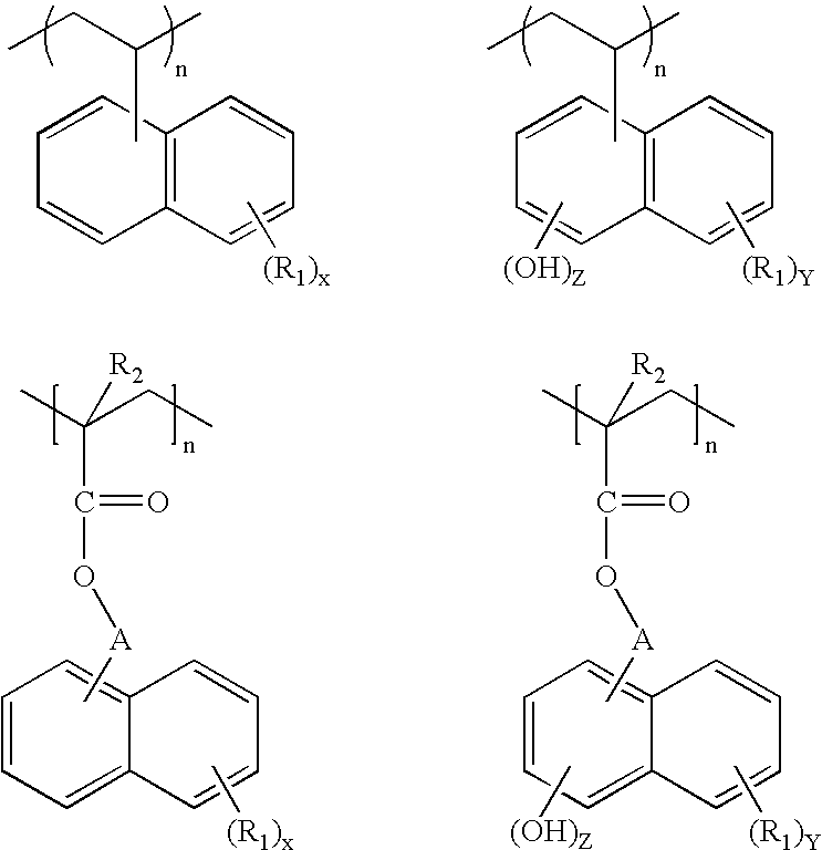

Priority Applications (5)
| Application Number | Priority Date | Filing Date | Title |
|---|---|---|---|
| US11/195,566 US7439302B2 (en) | 2004-12-16 | 2005-08-02 | Low refractive index polymers as underlayers for silicon-containing photoresists |
| CN2005800431800A CN101080669B (en) | 2004-12-16 | 2005-11-30 | Low refractive index polymers as underlayers for silicon-containing photoresists |
| EP05857596A EP1825325A4 (en) | 2004-12-16 | 2005-11-30 | Low refractive index polymers as underlayers for silicon-containing photoresists |
| JP2007546713A JP5220418B2 (en) | 2004-12-16 | 2005-11-30 | Low refractive index polymer as the base layer for silicon-containing photoresists |
| PCT/US2005/043210 WO2006096221A1 (en) | 2004-12-16 | 2005-11-30 | Low refractive index polymers as underlayers for silicon-containing photoresists |
Applications Claiming Priority (2)
| Application Number | Priority Date | Filing Date | Title |
|---|---|---|---|
| US11/013,971 US7326523B2 (en) | 2004-12-16 | 2004-12-16 | Low refractive index polymers as underlayers for silicon-containing photoresists |
| US11/195,566 US7439302B2 (en) | 2004-12-16 | 2005-08-02 | Low refractive index polymers as underlayers for silicon-containing photoresists |
Related Parent Applications (1)
| Application Number | Title | Priority Date | Filing Date |
|---|---|---|---|
| US11/013,971 Continuation-In-Part US7326523B2 (en) | 2004-12-16 | 2004-12-16 | Low refractive index polymers as underlayers for silicon-containing photoresists |
Publications (2)
| Publication Number | Publication Date |
|---|---|
| US20060134547A1 true US20060134547A1 (en) | 2006-06-22 |
| US7439302B2 US7439302B2 (en) | 2008-10-21 |
Family
ID=36596301
Family Applications (2)
| Application Number | Title | Priority Date | Filing Date |
|---|---|---|---|
| US11/013,971 Expired - Fee Related US7326523B2 (en) | 2004-12-16 | 2004-12-16 | Low refractive index polymers as underlayers for silicon-containing photoresists |
| US11/195,566 Active 2025-09-16 US7439302B2 (en) | 2004-12-16 | 2005-08-02 | Low refractive index polymers as underlayers for silicon-containing photoresists |
Family Applications Before (1)
| Application Number | Title | Priority Date | Filing Date |
|---|---|---|---|
| US11/013,971 Expired - Fee Related US7326523B2 (en) | 2004-12-16 | 2004-12-16 | Low refractive index polymers as underlayers for silicon-containing photoresists |
Country Status (3)
| Country | Link |
|---|---|
| US (2) | US7326523B2 (en) |
| JP (1) | JP5220418B2 (en) |
| CN (1) | CN101080669B (en) |
Cited By (20)
| Publication number | Priority date | Publication date | Assignee | Title |
|---|---|---|---|---|
| US20070087285A1 (en) * | 2005-10-13 | 2007-04-19 | International Business Machines Corporation | Top antireflective coating composition with low refractive index at 193nm radiation wavelength |
| US20080311508A1 (en) * | 2006-02-17 | 2008-12-18 | Internation Business Machines Corporation | Process of making a semiconductor device using multiple antireflective materials |
| US20090035704A1 (en) * | 2007-08-03 | 2009-02-05 | Hong Zhuang | Underlayer Coating Composition Based on a Crosslinkable Polymer |
| US20090042133A1 (en) * | 2007-08-10 | 2009-02-12 | Zhong Xiang | Antireflective Coating Composition |
| US20090130591A1 (en) * | 2007-11-21 | 2009-05-21 | Huirong Yao | Antireflective Coating Composition and Process Thereof |
| US20100009293A1 (en) * | 2008-07-08 | 2010-01-14 | Huirong Yao | Antireflective Coating Compositions |
| US20100009297A1 (en) * | 2008-07-08 | 2010-01-14 | Huirong Yao | Antireflective Coating Compositions |
| US20100081079A1 (en) * | 2008-09-30 | 2010-04-01 | Korea Kumho Petrochemical Co., Ltd. | Polymer for resist and resist composition manufactured using the same |
| US7691556B2 (en) | 2004-09-15 | 2010-04-06 | Az Electronic Materials Usa Corp. | Antireflective compositions for photoresists |
| US20100092894A1 (en) * | 2008-10-14 | 2010-04-15 | Weihong Liu | Bottom Antireflective Coating Compositions |
| US20100096663A1 (en) * | 2007-05-17 | 2010-04-22 | Nissan Chemical Industries, Ltd. | Photosensitive resin and process for producing microlens |
| US20100273321A1 (en) * | 2009-04-27 | 2010-10-28 | Taiwan Semiconductor Manufacturing Company, Ltd. | Wet soluble lithography |
| US20100285410A1 (en) * | 2009-05-11 | 2010-11-11 | Taiwan Semiconductor Manufacturing Company, Ltd. | Method For Manufacturing A Semiconductor Device Using A Modified Photosensitive Layer |
| US20110200938A1 (en) * | 2010-02-18 | 2011-08-18 | Huirong Yao | Antireflective Compositions and Methods of Using Same |
| US20110200941A1 (en) * | 2010-02-16 | 2011-08-18 | Keiichi Masunaga | Chemically amplified positive resist composition for eb or euv lithography and patterning process |
| US20110200942A1 (en) * | 2010-02-16 | 2011-08-18 | Keiichi Masunaga | Chemically amplified negative resist composition for eb or euv lithography and patterning process |
| US8445181B2 (en) | 2010-06-03 | 2013-05-21 | Az Electronic Materials Usa Corp. | Antireflective coating composition and process thereof |
| US20170003592A1 (en) * | 2014-03-24 | 2017-01-05 | Jsr Corporation | Pattern-forming method |
| US20170045819A1 (en) * | 2014-05-22 | 2017-02-16 | Nissan Chemical Industries, Ltd. | Resist underlayer film-forming composition for lithography containing polymer having acrylamide structure and acrylic acid ester structure |
| US10381481B1 (en) | 2018-04-27 | 2019-08-13 | Taiwan Semiconductor Manufacturing Co., Ltd. | Multi-layer photoresist |
Families Citing this family (13)
| Publication number | Priority date | Publication date | Assignee | Title |
|---|---|---|---|---|
| JP5112733B2 (en) | 2006-04-11 | 2013-01-09 | ローム・アンド・ハース・エレクトロニック・マテリアルズ,エル.エル.シー. | Coating composition for photolithography |
| JP5337398B2 (en) * | 2007-04-06 | 2013-11-06 | ローム・アンド・ハース・エレクトロニック・マテリアルズ,エル.エル.シー. | Coating composition |
| US8084193B2 (en) * | 2008-07-12 | 2011-12-27 | International Business Machines Corporation | Self-segregating multilayer imaging stack with built-in antireflective properties |
| JP5708938B2 (en) * | 2010-01-18 | 2015-04-30 | 日産化学工業株式会社 | Photosensitive resist underlayer film forming composition and resist pattern forming method |
| JPWO2012081619A1 (en) * | 2010-12-17 | 2014-05-22 | 日産化学工業株式会社 | Resist underlayer film forming composition and resist pattern forming method using the same |
| US8455312B2 (en) * | 2011-09-12 | 2013-06-04 | Cindy X. Qiu | Fabrication methods for T-gate and inverted L-gate structure for high frequency devices and circuits |
| CN103365094B (en) * | 2012-04-09 | 2015-09-02 | 中芯国际集成电路制造(上海)有限公司 | Dual photoresist structure and disposal route thereof |
| KR20170141278A (en) | 2013-01-28 | 2017-12-22 | 닛뽕소다 가부시키가이샤 | Coating agent |
| KR101771542B1 (en) | 2014-07-15 | 2017-09-05 | 삼성에스디아이 주식회사 | Hardmask composition and method of forming patterns using the hardmask composition |
| US10684546B2 (en) * | 2016-04-28 | 2020-06-16 | Nissan Chemical Corporation | Composition for forming resist underlayer film |
| JP6944255B2 (en) * | 2017-03-14 | 2021-10-06 | Hoya株式会社 | Manufacturing method of transfer mask and manufacturing method of semiconductor device |
| WO2019065246A1 (en) * | 2017-09-28 | 2019-04-04 | 日本ゼオン株式会社 | Resin composition and resin film |
| CN108997579B (en) * | 2018-07-31 | 2021-04-06 | 湖南工业大学 | Aromatic hyperbranched polyimide containing anthracene structure and preparation method and application thereof |
Citations (20)
| Publication number | Priority date | Publication date | Assignee | Title |
|---|---|---|---|---|
| US2739956A (en) * | 1953-06-15 | 1956-03-27 | Eastman Kodak Co | Methoxy vinylnaphthalenes and polymers thereof |
| US3575925A (en) * | 1968-06-17 | 1971-04-20 | Nat Starch Chem Corp | Photosensitive coating systems |
| US4592993A (en) * | 1980-11-05 | 1986-06-03 | Nippon Electric Co., Ltd. | Pattern forming and etching process using radiation sensitive negative resist |
| US4855017A (en) * | 1985-05-03 | 1989-08-08 | Texas Instruments Incorporated | Trench etch process for a single-wafer RIE dry etch reactor |
| US5362663A (en) * | 1992-01-09 | 1994-11-08 | International Business Machines Corporation | Method of forming double well substrate plate trench DRAM cell array |
| US5429710A (en) * | 1993-02-25 | 1995-07-04 | Sony Corporation | Dry etching method |
| US5443690A (en) * | 1993-05-12 | 1995-08-22 | Fujitsu Limited | Pattern formation material and pattern formation method |
| US5562801A (en) * | 1994-04-28 | 1996-10-08 | Cypress Semiconductor Corporation | Method of etching an oxide layer |
| US5618751A (en) * | 1996-05-23 | 1997-04-08 | International Business Machines Corporation | Method of making single-step trenches using resist fill and recess |
| US5663036A (en) * | 1994-12-13 | 1997-09-02 | International Business Machines Corporation | Microlithographic structure with an underlayer film comprising a thermolyzed azide |
| US5744376A (en) * | 1996-04-08 | 1998-04-28 | Chartered Semiconductor Manufacturing Pte, Ltd | Method of manufacturing copper interconnect with top barrier layer |
| US5801094A (en) * | 1997-02-28 | 1998-09-01 | United Microelectronics Corporation | Dual damascene process |
| US5861231A (en) * | 1996-06-11 | 1999-01-19 | Shipley Company, L.L.C. | Copolymers and photoresist compositions comprising copolymer resin binder component |
| US5919599A (en) * | 1997-09-30 | 1999-07-06 | Brewer Science, Inc. | Thermosetting anti-reflective coatings at deep ultraviolet |
| US6261743B1 (en) * | 1997-02-07 | 2001-07-17 | Shipley Company, L.L.C. | Antireflective coating compositions comprising photoacid generators |
| US20020076641A1 (en) * | 2000-09-07 | 2002-06-20 | Samsung Electronics Co., Ltd. | Photosensitive polymer having fused aromatic ring and photoresist composition containing the same |
| US20020094382A1 (en) * | 2000-12-01 | 2002-07-18 | Kansai Paint Co., Ltd. | Method of forming conductive pattern |
| US20020173594A1 (en) * | 1999-03-12 | 2002-11-21 | Arch Specialty Chemicals, Inc. | Thermally cured underlayer for lithographic application |
| US20030134224A1 (en) * | 2001-07-03 | 2003-07-17 | Fuji Photo Film Co., Ltd. | Positive resist composition |
| US20040058272A1 (en) * | 2002-09-06 | 2004-03-25 | Fuji Photo Film Co., Ltd. | Resist composition |
Family Cites Families (24)
| Publication number | Priority date | Publication date | Assignee | Title |
|---|---|---|---|---|
| DE3265701D1 (en) | 1981-02-13 | 1985-10-03 | Ciba Geigy Ag | Curable compositions containing an acid-curable resin, and process for curing them |
| JPS60116132A (en) | 1983-11-29 | 1985-06-22 | Fujitsu Ltd | Forming method of negative type resist pattern |
| JPH01293339A (en) | 1988-05-23 | 1989-11-27 | Tosoh Corp | Photoresist composition |
| US6165282A (en) | 1992-06-30 | 2000-12-26 | Southwest Research Institute | Method for contaminant removal using natural convection flow and changes in solubility concentration by temperature |
| US5948570A (en) | 1995-05-26 | 1999-09-07 | Lucent Technologies Inc. | Process for dry lithographic etching |
| US5886102A (en) | 1996-06-11 | 1999-03-23 | Shipley Company, L.L.C. | Antireflective coating compositions |
| US5962184A (en) | 1996-12-13 | 1999-10-05 | International Business Machines Corporation | Photoresist composition comprising a copolymer of a hydroxystyrene and a (meth)acrylate substituted with an alicyclic ester substituent |
| US6808869B1 (en) * | 1996-12-24 | 2004-10-26 | Fuji Photo Film Co., Ltd. | Bottom anti-reflective coating material composition and method for forming resist pattern using the same |
| JP3851402B2 (en) * | 1997-02-28 | 2006-11-29 | 富士写真フイルム株式会社 | Antireflection film material composition and resist pattern forming method using the same |
| US5985524A (en) | 1997-03-28 | 1999-11-16 | International Business Machines Incorporated | Process for using bilayer photoresist |
| US6037097A (en) | 1998-01-27 | 2000-03-14 | International Business Machines Corporation | E-beam application to mask making using new improved KRS resist system |
| US6087064A (en) | 1998-09-03 | 2000-07-11 | International Business Machines Corporation | Silsesquioxane polymers, method of synthesis, photoresist composition, and multilayer lithographic method |
| US6054248A (en) | 1999-03-12 | 2000-04-25 | Arch Specialty Chemicals, Inc. | Hydroxy-diisocyanate thermally cured undercoat for 193 nm lithography |
| JP3989149B2 (en) * | 1999-12-16 | 2007-10-10 | 富士フイルム株式会社 | Chemical amplification negative resist composition for electron beam or X-ray |
| US6444408B1 (en) | 2000-02-28 | 2002-09-03 | International Business Machines Corporation | High silicon content monomers and polymers suitable for 193 nm bilayer resists |
| US6420088B1 (en) | 2000-06-23 | 2002-07-16 | International Business Machines Corporation | Antireflective silicon-containing compositions as hardmask layer |
| JP3971088B2 (en) * | 2000-06-30 | 2007-09-05 | 株式会社東芝 | Pattern formation method |
| US6869899B2 (en) | 2001-07-12 | 2005-03-22 | International Business Machines Corporation | Lateral-only photoresist trimming for sub-80 nm gate stack |
| US7244549B2 (en) | 2001-08-24 | 2007-07-17 | Jsr Corporation | Pattern forming method and bilayer film |
| US20030215736A1 (en) * | 2002-01-09 | 2003-11-20 | Oberlander Joseph E. | Negative-working photoimageable bottom antireflective coating |
| JP2003228167A (en) * | 2002-02-01 | 2003-08-15 | Fuji Photo Film Co Ltd | Negative resist composition |
| US6730454B2 (en) | 2002-04-16 | 2004-05-04 | International Business Machines Corporation | Antireflective SiO-containing compositions for hardmask layer |
| US7038328B2 (en) * | 2002-10-15 | 2006-05-02 | Brewer Science Inc. | Anti-reflective compositions comprising triazine compounds |
| EP1780600B1 (en) * | 2004-07-02 | 2014-02-26 | Nissan Chemical Industries, Ltd. | Lower layer film forming composition for lithography including naphthalene ring having halogen atom |
-
2004
- 2004-12-16 US US11/013,971 patent/US7326523B2/en not_active Expired - Fee Related
-
2005
- 2005-08-02 US US11/195,566 patent/US7439302B2/en active Active
- 2005-11-30 CN CN2005800431800A patent/CN101080669B/en not_active Expired - Fee Related
- 2005-11-30 JP JP2007546713A patent/JP5220418B2/en not_active Expired - Fee Related
Patent Citations (22)
| Publication number | Priority date | Publication date | Assignee | Title |
|---|---|---|---|---|
| US2739956A (en) * | 1953-06-15 | 1956-03-27 | Eastman Kodak Co | Methoxy vinylnaphthalenes and polymers thereof |
| US3575925A (en) * | 1968-06-17 | 1971-04-20 | Nat Starch Chem Corp | Photosensitive coating systems |
| US4592993A (en) * | 1980-11-05 | 1986-06-03 | Nippon Electric Co., Ltd. | Pattern forming and etching process using radiation sensitive negative resist |
| US4855017A (en) * | 1985-05-03 | 1989-08-08 | Texas Instruments Incorporated | Trench etch process for a single-wafer RIE dry etch reactor |
| US5362663A (en) * | 1992-01-09 | 1994-11-08 | International Business Machines Corporation | Method of forming double well substrate plate trench DRAM cell array |
| US5429710A (en) * | 1993-02-25 | 1995-07-04 | Sony Corporation | Dry etching method |
| US5443690A (en) * | 1993-05-12 | 1995-08-22 | Fujitsu Limited | Pattern formation material and pattern formation method |
| US5562801A (en) * | 1994-04-28 | 1996-10-08 | Cypress Semiconductor Corporation | Method of etching an oxide layer |
| US5783361A (en) * | 1994-12-13 | 1998-07-21 | International Business Machines Corporation | Microlithographic structure with an underlayer film containing a thermolyzed azide compound |
| US5795701A (en) * | 1994-12-13 | 1998-08-18 | International Business Machines Corporation | Making of microlithographic structures with an underlayer film containing a thermolyzed azide compound |
| US5663036A (en) * | 1994-12-13 | 1997-09-02 | International Business Machines Corporation | Microlithographic structure with an underlayer film comprising a thermolyzed azide |
| US5744376A (en) * | 1996-04-08 | 1998-04-28 | Chartered Semiconductor Manufacturing Pte, Ltd | Method of manufacturing copper interconnect with top barrier layer |
| US5618751A (en) * | 1996-05-23 | 1997-04-08 | International Business Machines Corporation | Method of making single-step trenches using resist fill and recess |
| US5861231A (en) * | 1996-06-11 | 1999-01-19 | Shipley Company, L.L.C. | Copolymers and photoresist compositions comprising copolymer resin binder component |
| US6261743B1 (en) * | 1997-02-07 | 2001-07-17 | Shipley Company, L.L.C. | Antireflective coating compositions comprising photoacid generators |
| US5801094A (en) * | 1997-02-28 | 1998-09-01 | United Microelectronics Corporation | Dual damascene process |
| US5919599A (en) * | 1997-09-30 | 1999-07-06 | Brewer Science, Inc. | Thermosetting anti-reflective coatings at deep ultraviolet |
| US20020173594A1 (en) * | 1999-03-12 | 2002-11-21 | Arch Specialty Chemicals, Inc. | Thermally cured underlayer for lithographic application |
| US20020076641A1 (en) * | 2000-09-07 | 2002-06-20 | Samsung Electronics Co., Ltd. | Photosensitive polymer having fused aromatic ring and photoresist composition containing the same |
| US20020094382A1 (en) * | 2000-12-01 | 2002-07-18 | Kansai Paint Co., Ltd. | Method of forming conductive pattern |
| US20030134224A1 (en) * | 2001-07-03 | 2003-07-17 | Fuji Photo Film Co., Ltd. | Positive resist composition |
| US20040058272A1 (en) * | 2002-09-06 | 2004-03-25 | Fuji Photo Film Co., Ltd. | Resist composition |
Cited By (35)
| Publication number | Priority date | Publication date | Assignee | Title |
|---|---|---|---|---|
| US7691556B2 (en) | 2004-09-15 | 2010-04-06 | Az Electronic Materials Usa Corp. | Antireflective compositions for photoresists |
| US7544750B2 (en) * | 2005-10-13 | 2009-06-09 | International Business Machines Corporation | Top antireflective coating composition with low refractive index at 193nm radiation wavelength |
| US20070087285A1 (en) * | 2005-10-13 | 2007-04-19 | International Business Machines Corporation | Top antireflective coating composition with low refractive index at 193nm radiation wavelength |
| US20080311508A1 (en) * | 2006-02-17 | 2008-12-18 | Internation Business Machines Corporation | Process of making a semiconductor device using multiple antireflective materials |
| US7968270B2 (en) * | 2006-02-17 | 2011-06-28 | International Business Machines Corporation | Process of making a semiconductor device using multiple antireflective materials |
| US8940470B2 (en) * | 2007-05-17 | 2015-01-27 | Nissan Chemical Industries, Inc. | Photosensitive resin and process for producing microlens |
| US20100096663A1 (en) * | 2007-05-17 | 2010-04-22 | Nissan Chemical Industries, Ltd. | Photosensitive resin and process for producing microlens |
| US20090035704A1 (en) * | 2007-08-03 | 2009-02-05 | Hong Zhuang | Underlayer Coating Composition Based on a Crosslinkable Polymer |
| US20090042133A1 (en) * | 2007-08-10 | 2009-02-12 | Zhong Xiang | Antireflective Coating Composition |
| US8039201B2 (en) * | 2007-11-21 | 2011-10-18 | Az Electronic Materials Usa Corp. | Antireflective coating composition and process thereof |
| US20090130591A1 (en) * | 2007-11-21 | 2009-05-21 | Huirong Yao | Antireflective Coating Composition and Process Thereof |
| US8329387B2 (en) | 2008-07-08 | 2012-12-11 | Az Electronic Materials Usa Corp. | Antireflective coating compositions |
| US20100009297A1 (en) * | 2008-07-08 | 2010-01-14 | Huirong Yao | Antireflective Coating Compositions |
| US20100009293A1 (en) * | 2008-07-08 | 2010-01-14 | Huirong Yao | Antireflective Coating Compositions |
| US8221965B2 (en) | 2008-07-08 | 2012-07-17 | Az Electronic Materials Usa Corp. | Antireflective coating compositions |
| US20100081079A1 (en) * | 2008-09-30 | 2010-04-01 | Korea Kumho Petrochemical Co., Ltd. | Polymer for resist and resist composition manufactured using the same |
| US8187790B2 (en) * | 2008-09-30 | 2012-05-29 | Korea Kumho Petrochemical Co., Ltd. | Polymer for resist and resist composition manufactured using the same |
| US20100092894A1 (en) * | 2008-10-14 | 2010-04-15 | Weihong Liu | Bottom Antireflective Coating Compositions |
| US20100273321A1 (en) * | 2009-04-27 | 2010-10-28 | Taiwan Semiconductor Manufacturing Company, Ltd. | Wet soluble lithography |
| US8822347B2 (en) * | 2009-04-27 | 2014-09-02 | Taiwan Semiconductor Manufacturing Company, Ltd. | Wet soluble lithography |
| US20100285410A1 (en) * | 2009-05-11 | 2010-11-11 | Taiwan Semiconductor Manufacturing Company, Ltd. | Method For Manufacturing A Semiconductor Device Using A Modified Photosensitive Layer |
| US8304179B2 (en) | 2009-05-11 | 2012-11-06 | Taiwan Semiconductor Manufacturing Company, Ltd. | Method for manufacturing a semiconductor device using a modified photosensitive layer |
| US20110200941A1 (en) * | 2010-02-16 | 2011-08-18 | Keiichi Masunaga | Chemically amplified positive resist composition for eb or euv lithography and patterning process |
| US8426108B2 (en) * | 2010-02-16 | 2013-04-23 | Shin-Etsu Chemical Co., Ltd. | Chemically amplified positive resist composition for EB or EUV lithography and patterning process |
| US8470511B2 (en) * | 2010-02-16 | 2013-06-25 | Shin-Etsu Chemical Co., Ltd. | Chemically amplified negative resist composition for EB or EUV lithography and patterning process |
| US20110200942A1 (en) * | 2010-02-16 | 2011-08-18 | Keiichi Masunaga | Chemically amplified negative resist composition for eb or euv lithography and patterning process |
| US8507192B2 (en) | 2010-02-18 | 2013-08-13 | Az Electronic Materials Usa Corp. | Antireflective compositions and methods of using same |
| US20110200938A1 (en) * | 2010-02-18 | 2011-08-18 | Huirong Yao | Antireflective Compositions and Methods of Using Same |
| US8445181B2 (en) | 2010-06-03 | 2013-05-21 | Az Electronic Materials Usa Corp. | Antireflective coating composition and process thereof |
| US20170003592A1 (en) * | 2014-03-24 | 2017-01-05 | Jsr Corporation | Pattern-forming method |
| US10234762B2 (en) * | 2014-03-24 | 2019-03-19 | Jsr Corporation | Pattern-forming method |
| US20170045819A1 (en) * | 2014-05-22 | 2017-02-16 | Nissan Chemical Industries, Ltd. | Resist underlayer film-forming composition for lithography containing polymer having acrylamide structure and acrylic acid ester structure |
| US10295907B2 (en) * | 2014-05-22 | 2019-05-21 | Nissan Chemical Industries, Ltd. | Resist underlayer film-forming composition for lithography containing polymer having acrylamide structure and acrylic acid ester structure |
| US10381481B1 (en) | 2018-04-27 | 2019-08-13 | Taiwan Semiconductor Manufacturing Co., Ltd. | Multi-layer photoresist |
| US10777681B2 (en) | 2018-04-27 | 2020-09-15 | Taiwan Semiconductor Manufacturing Co., Ltd. | Multi-layer photoresist |
Also Published As
| Publication number | Publication date |
|---|---|
| US7326523B2 (en) | 2008-02-05 |
| JP5220418B2 (en) | 2013-06-26 |
| CN101080669A (en) | 2007-11-28 |
| CN101080669B (en) | 2012-08-29 |
| US7439302B2 (en) | 2008-10-21 |
| US20060134546A1 (en) | 2006-06-22 |
| JP2008524382A (en) | 2008-07-10 |
Similar Documents
| Publication | Publication Date | Title |
|---|---|---|
| US7439302B2 (en) | Low refractive index polymers as underlayers for silicon-containing photoresists | |
| US6818381B2 (en) | Underlayer compositions for multilayer lithographic processes | |
| US8263321B2 (en) | Polymer having antireflective properties and high carbon content, hardmask composition including the same, and process for forming a patterned material layer | |
| US7276327B2 (en) | Silicon-containing compositions for spin-on arc/hardmask materials | |
| US8445187B2 (en) | Hardmask composition having antireflective properties and method of patterning material on substrate using the same | |
| US7655386B2 (en) | Polymer having antireflective properties, hardmask composition including the same, process for forming a patterned material layer, and associated device | |
| US9116429B2 (en) | Resist underlayer polymer, resist underlayer composition including the same, and method of patterning using the same | |
| KR101813311B1 (en) | Underlayer film-forming composition and pattern forming process | |
| US7659051B2 (en) | Polymer having antireflective properties, hardmask composition including the same, and process for forming a patterned material layer | |
| US9040225B2 (en) | Developable bottom antireflective coating composition and pattern forming method using thereof | |
| KR100697979B1 (en) | Antireflective hardmask composition | |
| KR20140144658A (en) | Underlayer film-forming composition and pattern forming process | |
| CN102695986B (en) | Polymer containing an aromatic ring for a resist underlayer, and resist underlayer compound including the polymer | |
| JP2013156647A (en) | Anti-reflective coating composition | |
| TWI411628B (en) | Underlayer composition having anti-reflective property | |
| US7638266B2 (en) | Ultrathin polymeric photoacid generator layer and method of fabricating at least one of a device and a mask by using said layer | |
| KR100865684B1 (en) | High etch resistant hardmask composition having antireflective property, method of manufacturing of patterning materials and semiconductor ic device produced by the method | |
| EP1825325A1 (en) | Low refractive index polymers as underlayers for silicon-containing photoresists | |
| KR100836675B1 (en) | Hardmask composition having antireflective property, process of producing patterned materials by using the same and integrated circuit devices |
Legal Events
| Date | Code | Title | Description |
|---|---|---|---|
| FEPP | Fee payment procedure |
Free format text: PAYOR NUMBER ASSIGNED (ORIGINAL EVENT CODE: ASPN); ENTITY STATUS OF PATENT OWNER: LARGE ENTITY |
|
| STCF | Information on status: patent grant |
Free format text: PATENTED CASE |
|
| REMI | Maintenance fee reminder mailed | ||
| FPAY | Fee payment |
Year of fee payment: 4 |
|
| SULP | Surcharge for late payment | ||
| AS | Assignment |
Owner name: INTERNATIONAL BUSINESS MACHINES CORPORATION, NEW Y Free format text: ASSIGNMENT OF ASSIGNORS INTEREST;ASSIGNORS:BURNS, SEAN D;HUANG, WU-SONG S;KHOJASTEH, MAHMOUD;SIGNING DATES FROM 20150109 TO 20150119;REEL/FRAME:034818/0380 |
|
| AS | Assignment |
Owner name: GLOBALFOUNDRIES U.S. 2 LLC, NEW YORK Free format text: ASSIGNMENT OF ASSIGNORS INTEREST;ASSIGNOR:INTERNATIONAL BUSINESS MACHINES CORPORATION;REEL/FRAME:036550/0001 Effective date: 20150629 |
|
| AS | Assignment |
Owner name: GLOBALFOUNDRIES INC., CAYMAN ISLANDS Free format text: ASSIGNMENT OF ASSIGNORS INTEREST;ASSIGNORS:GLOBALFOUNDRIES U.S. 2 LLC;GLOBALFOUNDRIES U.S. INC.;REEL/FRAME:036779/0001 Effective date: 20150910 |
|
| FPAY | Fee payment |
Year of fee payment: 8 |
|
| AS | Assignment |
Owner name: WILMINGTON TRUST, NATIONAL ASSOCIATION, DELAWARE Free format text: SECURITY AGREEMENT;ASSIGNOR:GLOBALFOUNDRIES INC.;REEL/FRAME:049490/0001 Effective date: 20181127 |
|
| MAFP | Maintenance fee payment |
Free format text: PAYMENT OF MAINTENANCE FEE, 12TH YEAR, LARGE ENTITY (ORIGINAL EVENT CODE: M1553); ENTITY STATUS OF PATENT OWNER: LARGE ENTITY Year of fee payment: 12 |
|
| AS | Assignment |
Owner name: GLOBALFOUNDRIES U.S. INC., CALIFORNIA Free format text: ASSIGNMENT OF ASSIGNORS INTEREST;ASSIGNOR:GLOBALFOUNDRIES INC.;REEL/FRAME:054633/0001 Effective date: 20201022 |
|
| AS | Assignment |
Owner name: GLOBALFOUNDRIES INC., CAYMAN ISLANDS Free format text: RELEASE BY SECURED PARTY;ASSIGNOR:WILMINGTON TRUST, NATIONAL ASSOCIATION;REEL/FRAME:054636/0001 Effective date: 20201117 |
|
| AS | Assignment |
Owner name: GLOBALFOUNDRIES U.S. INC., NEW YORK Free format text: RELEASE BY SECURED PARTY;ASSIGNOR:WILMINGTON TRUST, NATIONAL ASSOCIATION;REEL/FRAME:056987/0001 Effective date: 20201117 |