US20020171908A1 - Low dispersion interleaver - Google Patents
Low dispersion interleaver Download PDFInfo
- Publication number
- US20020171908A1 US20020171908A1 US10/058,534 US5853402A US2002171908A1 US 20020171908 A1 US20020171908 A1 US 20020171908A1 US 5853402 A US5853402 A US 5853402A US 2002171908 A1 US2002171908 A1 US 2002171908A1
- Authority
- US
- United States
- Prior art keywords
- etalon
- resonator
- cavity
- sub
- effective
- Prior art date
- Legal status (The legal status is an assumption and is not a legal conclusion. Google has not performed a legal analysis and makes no representation as to the accuracy of the status listed.)
- Granted
Links
Images


Classifications
-
- G—PHYSICS
- G02—OPTICS
- G02B—OPTICAL ELEMENTS, SYSTEMS OR APPARATUS
- G02B6/00—Light guides; Structural details of arrangements comprising light guides and other optical elements, e.g. couplings
- G02B6/10—Light guides; Structural details of arrangements comprising light guides and other optical elements, e.g. couplings of the optical waveguide type
- G02B6/12—Light guides; Structural details of arrangements comprising light guides and other optical elements, e.g. couplings of the optical waveguide type of the integrated circuit kind
- G02B6/12007—Light guides; Structural details of arrangements comprising light guides and other optical elements, e.g. couplings of the optical waveguide type of the integrated circuit kind forming wavelength selective elements, e.g. multiplexer, demultiplexer
-
- G—PHYSICS
- G02—OPTICS
- G02B—OPTICAL ELEMENTS, SYSTEMS OR APPARATUS
- G02B6/00—Light guides; Structural details of arrangements comprising light guides and other optical elements, e.g. couplings
- G02B6/24—Coupling light guides
- G02B6/26—Optical coupling means
- G02B6/28—Optical coupling means having data bus means, i.e. plural waveguides interconnected and providing an inherently bidirectional system by mixing and splitting signals
- G02B6/293—Optical coupling means having data bus means, i.e. plural waveguides interconnected and providing an inherently bidirectional system by mixing and splitting signals with wavelength selective means
- G02B6/29302—Optical coupling means having data bus means, i.e. plural waveguides interconnected and providing an inherently bidirectional system by mixing and splitting signals with wavelength selective means based on birefringence or polarisation, e.g. wavelength dependent birefringence, polarisation interferometers
-
- G—PHYSICS
- G02—OPTICS
- G02B—OPTICAL ELEMENTS, SYSTEMS OR APPARATUS
- G02B6/00—Light guides; Structural details of arrangements comprising light guides and other optical elements, e.g. couplings
- G02B6/24—Coupling light guides
- G02B6/26—Optical coupling means
- G02B6/28—Optical coupling means having data bus means, i.e. plural waveguides interconnected and providing an inherently bidirectional system by mixing and splitting signals
- G02B6/293—Optical coupling means having data bus means, i.e. plural waveguides interconnected and providing an inherently bidirectional system by mixing and splitting signals with wavelength selective means
- G02B6/29346—Optical coupling means having data bus means, i.e. plural waveguides interconnected and providing an inherently bidirectional system by mixing and splitting signals with wavelength selective means operating by wave or beam interference
- G02B6/29347—Loop interferometers, e.g. Sagnac, loop mirror
-
- G—PHYSICS
- G02—OPTICS
- G02B—OPTICAL ELEMENTS, SYSTEMS OR APPARATUS
- G02B6/00—Light guides; Structural details of arrangements comprising light guides and other optical elements, e.g. couplings
- G02B6/24—Coupling light guides
- G02B6/26—Optical coupling means
- G02B6/28—Optical coupling means having data bus means, i.e. plural waveguides interconnected and providing an inherently bidirectional system by mixing and splitting signals
- G02B6/293—Optical coupling means having data bus means, i.e. plural waveguides interconnected and providing an inherently bidirectional system by mixing and splitting signals with wavelength selective means
- G02B6/29346—Optical coupling means having data bus means, i.e. plural waveguides interconnected and providing an inherently bidirectional system by mixing and splitting signals with wavelength selective means operating by wave or beam interference
- G02B6/29349—Michelson or Michelson/Gires-Tournois configuration, i.e. based on splitting and interferometrically combining relatively delayed signals at a single beamsplitter
-
- G—PHYSICS
- G02—OPTICS
- G02B—OPTICAL ELEMENTS, SYSTEMS OR APPARATUS
- G02B6/00—Light guides; Structural details of arrangements comprising light guides and other optical elements, e.g. couplings
- G02B6/24—Coupling light guides
- G02B6/26—Optical coupling means
- G02B6/28—Optical coupling means having data bus means, i.e. plural waveguides interconnected and providing an inherently bidirectional system by mixing and splitting signals
- G02B6/293—Optical coupling means having data bus means, i.e. plural waveguides interconnected and providing an inherently bidirectional system by mixing and splitting signals with wavelength selective means
- G02B6/29346—Optical coupling means having data bus means, i.e. plural waveguides interconnected and providing an inherently bidirectional system by mixing and splitting signals with wavelength selective means operating by wave or beam interference
- G02B6/2935—Mach-Zehnder configuration, i.e. comprising separate splitting and combining means
- G02B6/29352—Mach-Zehnder configuration, i.e. comprising separate splitting and combining means in a light guide
-
- G—PHYSICS
- G02—OPTICS
- G02B—OPTICAL ELEMENTS, SYSTEMS OR APPARATUS
- G02B6/00—Light guides; Structural details of arrangements comprising light guides and other optical elements, e.g. couplings
- G02B6/24—Coupling light guides
- G02B6/26—Optical coupling means
- G02B6/28—Optical coupling means having data bus means, i.e. plural waveguides interconnected and providing an inherently bidirectional system by mixing and splitting signals
- G02B6/293—Optical coupling means having data bus means, i.e. plural waveguides interconnected and providing an inherently bidirectional system by mixing and splitting signals with wavelength selective means
- G02B6/29346—Optical coupling means having data bus means, i.e. plural waveguides interconnected and providing an inherently bidirectional system by mixing and splitting signals with wavelength selective means operating by wave or beam interference
- G02B6/29358—Multiple beam interferometer external to a light guide, e.g. Fabry-Pérot, etalon, VIPA plate, OTDL plate, continuous interferometer, parallel plate resonator
-
- G—PHYSICS
- G02—OPTICS
- G02B—OPTICAL ELEMENTS, SYSTEMS OR APPARATUS
- G02B6/00—Light guides; Structural details of arrangements comprising light guides and other optical elements, e.g. couplings
- G02B6/24—Coupling light guides
- G02B6/26—Optical coupling means
- G02B6/28—Optical coupling means having data bus means, i.e. plural waveguides interconnected and providing an inherently bidirectional system by mixing and splitting signals
- G02B6/293—Optical coupling means having data bus means, i.e. plural waveguides interconnected and providing an inherently bidirectional system by mixing and splitting signals with wavelength selective means
- G02B6/29379—Optical coupling means having data bus means, i.e. plural waveguides interconnected and providing an inherently bidirectional system by mixing and splitting signals with wavelength selective means characterised by the function or use of the complete device
- G02B6/2938—Optical coupling means having data bus means, i.e. plural waveguides interconnected and providing an inherently bidirectional system by mixing and splitting signals with wavelength selective means characterised by the function or use of the complete device for multiplexing or demultiplexing, i.e. combining or separating wavelengths, e.g. 1xN, NxM
- G02B6/29386—Interleaving or deinterleaving, i.e. separating or mixing subsets of optical signals, e.g. combining even and odd channels into a single optical signal
-
- G—PHYSICS
- G02—OPTICS
- G02B—OPTICAL ELEMENTS, SYSTEMS OR APPARATUS
- G02B6/00—Light guides; Structural details of arrangements comprising light guides and other optical elements, e.g. couplings
- G02B6/24—Coupling light guides
- G02B6/26—Optical coupling means
- G02B6/27—Optical coupling means with polarisation selective and adjusting means
- G02B6/2706—Optical coupling means with polarisation selective and adjusting means as bulk elements, i.e. free space arrangements external to a light guide, e.g. polarising beam splitters
- G02B6/2713—Optical coupling means with polarisation selective and adjusting means as bulk elements, i.e. free space arrangements external to a light guide, e.g. polarising beam splitters cascade of polarisation selective or adjusting operations
- G02B6/272—Optical coupling means with polarisation selective and adjusting means as bulk elements, i.e. free space arrangements external to a light guide, e.g. polarising beam splitters cascade of polarisation selective or adjusting operations comprising polarisation means for beam splitting and combining
-
- G—PHYSICS
- G02—OPTICS
- G02B—OPTICAL ELEMENTS, SYSTEMS OR APPARATUS
- G02B6/00—Light guides; Structural details of arrangements comprising light guides and other optical elements, e.g. couplings
- G02B6/24—Coupling light guides
- G02B6/26—Optical coupling means
- G02B6/27—Optical coupling means with polarisation selective and adjusting means
- G02B6/2753—Optical coupling means with polarisation selective and adjusting means characterised by their function or use, i.e. of the complete device
- G02B6/2766—Manipulating the plane of polarisation from one input polarisation to another output polarisation, e.g. polarisation rotators, linear to circular polarisation converters
-
- G—PHYSICS
- G02—OPTICS
- G02B—OPTICAL ELEMENTS, SYSTEMS OR APPARATUS
- G02B6/00—Light guides; Structural details of arrangements comprising light guides and other optical elements, e.g. couplings
- G02B6/24—Coupling light guides
- G02B6/26—Optical coupling means
- G02B6/27—Optical coupling means with polarisation selective and adjusting means
- G02B6/2753—Optical coupling means with polarisation selective and adjusting means characterised by their function or use, i.e. of the complete device
- G02B6/2773—Polarisation splitting or combining
Definitions
- This invention relates to interferometers for use in optical communication networks, and more specifically to optical signal interleavers/deinterleavers designed to produce greatly reduced amounts of chromatic dispersion.
- a single optical fiber typically carries multiple independent data channels with each data channel assigned to a different optical wavelength.
- WDM wavelength division multiplexed
- Such networks are referred to as wavelength division multiplexed (WDM) networks.
- WDM wavelength division multiplexed
- data for different channels may be separated or combined using an optical frequency filter, in particular, an interleaver/deinterleaver (hereafter “interleaver”).
- An interleaver is a type of optical multiplexer which, when operating as an interleaver, combines subsets of channels from different fibers into a single optical beam.
- the interleaver When operating as a deinterleaver, the interleaver separates a single optical beam having a series of channels into two or more subset series of channels.
- an interleaver is used to separate or combine even and odd International Telecommunications Union (ITU) channels.
- ITU International Telecommunications Union
- FIG. 1 conceptually illustrates the function of an interleaver.
- the interleaver receives a first optical beam 100 , which comprises a number of even channels at frequencies f 2 , f 4 , f 6 .
- the frequencies of each channel are such that each of these channels is separated by the same amount, e.g. 100 GHz.
- the interleaver also receives a second optical beam 102 , which comprises a number of odd channels at frequencies f 1 , f 3 , f 5 . Similar to beam 100 , the frequencies of each of these channels are such that these channels are separated by the same amount, e.g. 100 GHz.
- the even and odd channels are offset from each other, normally an amount equal to half their separation distances, e.g. 50 GHz.
- the interleaver then interleaves the beams 100 and 102 to generate a beam 104 with the channels f 1 , f 2 , f 3 , f 4 , f 5 , f 6 , which are separated by 50 GHz.
- beam 104 is received and divided into beams 100 and 102 .
- Optical frequency interleavers are widely recognized as key components enabling the rapid expansion of WDM networks to higher channel counts and narrower channel spacing, while preserving inter-channel cross-talk performance, in combination with existing demultiplexer technologies. Because of the periodic frequency nature of the International Telecommunications Union (ITU) grid, interleavers tend to be constructed from combinations of one or more interferometric structures, such as etalons and Mach-Zehnder interferometers. The desirable features of interleaver pass bands include a flattop and high isolation in the stop-band.
- ITU International Telecommunications Union
- a Michelson interferometer uses a beamsplitter and two reflecting mirrors to separate wavelengths of a light signal into different optical paths. This type of interferometer provides a linear phase ramp dependent on the optical path difference between the two arms of the interferometer. The linear phase ramp generates a non-flat top response with no chromatic dispersion.
- an interferometer 200 comprises a beam splitter 202 (typically an approximately ⁇ fraction (50/50) ⁇ splitter), a plate 204 with a highly reflective (near 100%) coating 206 placed in one arm with spacers 207 a and 207 b preferably made from ultra low expansion material (ULE).
- a GT etalon 220 is placed in the other arm.
- the GT etalon 220 comprises a front plate 208 with a partially reflective (e.g., 15% reflectivity) coating 210 , spacers 211 a and 211 b preferably made from ultra low expansion material (ULE) and a back plate 214 with a highly reflective (near 100%) coating 212 . As shown, a gap of distance d separates front plate 208 and back plate 214 of the GT etalon 220 . Further, the GT etalon 220 is placed a distance L 2 from the beam splitter 202 , and the plate 206 is placed a distance L 1 from the beam splitter 202 .
- a partially reflective (e.g., 15% reflectivity) coating 210 spacers 211 a and 211 b preferably made from ultra low expansion material (ULE) and a back plate 214 with a highly reflective (near 100%) coating 212 .
- UEE ultra low expansion material
- a gap of distance d separates front plate 208 and back plate 214 of
- an incident beam B 1 comprising, for example, ITU even and odd channels is directed towards beam splitter 202 .
- Beam B 1 is split at splitter interface 222 into a beam B 3 and beam B 2 .
- Beam B 3 is directed towards plate 204 with highly reflective coating 206
- beam B 2 is directed towards GT etalon 220 .
- beam B 3 is reflected back to splitter 202 .
- Beam B 3 experiences a linear phase change per wavelength based upon the distance traveled from the splitter interface to plate 204 and back.
- An exemplary linear phase ramp of beam B 3 at splitter interface 222 is illustrated in FIG. 2 c as line 242 .
- beam B 2 is reflected back to splitter 202 .
- R is the power of reflectance of coating 210
- ⁇ is the vacuum wavelength
- ⁇ is the refractive index of the material inside GT etalon 220 .
- the material inside GT etalon 220 is air, resulting in a refractive index ⁇ equal to approximately 1.
- An exemplary non-linear phase ramp of beam B 2 at splitter interface 222 is illustrated in FIG. 2 c as line 240 for a 15% reflectivity of coating 210 .
- optical path difference ⁇ L is the difference between the distance L 1 and L 2 (i.e., L 1 ⁇ L 2 ).
- phase graphs illustrated in FIG. 2 c result when MGTI 200 is designed such that the optical path difference, ⁇ L, is one half, or multiples of one half, the GT air gap, d.
- GT etalon 220 perturbs the linear phase ramp of the interferometer 200 and produces a non-linear phase ramp.
- this non-linear phase ramp generates a flat top response function that is desired in telecommunication systems.
- ⁇ 2 ⁇ ⁇ ⁇ ⁇ d ⁇ + 2 ⁇ tan - 1 ⁇ [ 1 - R 1 + R ⁇ tan ⁇ ( 2 ⁇ ⁇ ⁇ ⁇ d ⁇ ) ]
- beam B 2 and B 3 meet at the splitter interface, part of beam B 2 is reflected, while part of beam B 3 is passed through, thereby forming beam B 4 .
- FIG. 2 c at the frequencies where these two portions are substantially 180° (i.e. ⁇ ) out of phase, destructive interference occurs, while constructive interference occurs at the frequencies where these two portions are substantially in phase.
- This spectral response is illustrated in FIG. 2 b as line 230 .
- This spectral response results in beam B 4 carrying a first sub-set of channels (e.g., the even channels).
- This spectral response is illustrated in FIG. 2 b as line 232 . This results in beam B 5 carrying a second sub-set of channels (e.g., the odd).
- the shape of the spectral responses of MGTI 200 is determined by the reflectivity of reflective coating 210 , while the period between transmission peaks, i.e. the interleaver free spectral range (FSR int ), of the spectral response is determined by the gap distance d of GT etalon 220 .
- interleaver Another type of interleaver (herein after referred to a “SEI”) is disclosed in U.S. Pat. No. 6,125,220 issued Sep. 26, 2000 to Copner et al, and U.S. Pat. No. 6,281,977 issued Aug. 28, 2001 in the name of J D S Fitel, which are both incorporated herein by reference.
- SEI serial-to-semiconductor
- the present invention provides for an interferometer comprising a beamsplitter and two optical resonators, e.g. GT etalons or ring resonators.
- the beamsplitter splits an input beam of light into a first sub-beam directed to follow a first path and a second sub-beam directed to follow a second path.
- the first resonator has a first effective cavity length and receives the first sub-beam.
- the second resonator has a second effective cavity length and receives the second sub-beam.
- the first path and the second path have an effective optical path difference approximately equal to one-half the first effective cavity length.
- the reflectivities of the front plates of the GT etalons are different, and are selected to provide a desired spectral response.
- the ratio of the reflectivities of the front plates should range from between 8:1 to 30:1.
- Some examples of reflectivities include: 45% and 4.5%, 35% and 2.5%, etc.
- the higher front reflectivity is selected from between 10%-90%, and more preferably between 25%-60%.
- the lower reflectivity plate varies from 1% to 10%.
- the two resonators are slightly de-phased from one another such that the dispersion slope of the first resonator is oppositely aligned, and preferably equal, with the dispersion slope of the second etalon, so that the overall dispersion of the device is greatly reduced.
- Another aspect of the present invention relates to an interferometer with a predetermined free spectral range (FSR) comprising:
- a polarization dependent delay section to produce an effective optical path difference of approximately L between orthogonally polarized components of an input beam of light
- a resonator optically coupled to said polarization dependent delay section, having a cavity length of substantially 2L;
- Another aspect of the present invention relates to an interferometer with a predetermined free spectral range (FSR) comprising:
- a optical resonator having a first port for launching an input beam of light, a second port for outputting reflected light from the resonator, a third port for outputting transmitted light from the resonator, and an effective cavity length; and first coupling means for combining the reflected and transmitted light from the optical resonator, wherein the reflected and transmitted light have a first effective optical path length difference between the optical resonator and the first coupling means of approximately half the effective cavity length.
- the aforementioned interferometer further comprises second coupling means for combining the reflected and transmitted light from the optical resonator, wherein the reflected light and the transmitted light have a second effective optical path length difference between the of approximately +/ ⁇ n( ⁇ c /4) or +/ ⁇ n(FSR/2), wherein ⁇ c is the center wavelength of the input beam of light, and n is an integer.
- FIG. 1 conceptually illustrates the function of an interleaver
- FIG. 2 a illustrates a standard Michelson interferometer with one mirror replaced with a Gires Tournois etalon (an MGTI) used as an interleaver;
- FIGS. 2 b and 2 c illustrate the spectral response and phase ramps, respectively, of an MGTI
- FIG. 3 a illustrates an interferometer according to the principles of the present invention
- FIG. 4 illustrates spectral responses of one embodiment of the present invention for a reflectivity ratio of 10:1 for a number of R1 reflectivities between 44-50% and the spectral response of an MGTI;
- FIG. 5 a illustrates another embodiment of an interferometer according to the principles of the present invention in which the two etalons are slightly de-phased from one another so as to reduce chromatic dispersion;
- FIG. 5 b illustrates how the dispersion profiles from the two GT's of FIG. 5 a align
- FIG. 5 c illustrates an example spectral intensity profile of the embodiment of FIG. 5 a designed as a 25 GHz interleaver
- FIG. 5 d illustrates an example dispersion profile of the embodiment of FIG. 5 a designed as a 25 GHz interleaver
- FIG. 6 a illustrates a top view of a polarization-based implementation of the embodiment of FIG. 5 a
- FIG. 6 b illustrates a side view of the polarization-based implementation of the embodiment of FIG. 6 a
- FIGS. 6 c and 6 d illustrate alternate embodiments of the phase delay section of the polarization-based implementation of the embodiment of FIG. 6 a;
- FIG. 7 a illustrates an alternate manner of injecting optical beams into the interferometer 300 or interferometer 500 ;
- FIG. 7 b illustrates the alternative manner of injecting optical beams of FIG. 7 a in use in a polarization dependent embodiment
- FIG. 8 a illustrates an alternate construction of the interferometer 300 or the interferometer 500 using a plate beam splitter 802 ;
- FIG. 8 b illustrates an alternative construction of the interferometer of FIG. 8 a using ring resonators
- FIG. 9 illustrates an embodiment to create two de-phased GT etalons using the fact that the resonance peak of a GT etalon changes as the angle of the incident beam is varied;
- FIG. 10 a illustrates an embodiment to further reduce the chromatic dispersion in the embodiment of FIG. 5 a;
- FIG. 10 b illustrates exemplary dispersion profiles for the cascaded interferometer of FIG. 10 a
- FIG. 10 c illustrates an exemplary resultant dispersion profile of the embodiment of FIG. 10 a
- FIGS. 10 d and 10 e collectively, conceptually illustrate the resulting spectral response of the embodiment of FIG. 10 a;
- FIG. 11 a conceptually illustrates another embodiment to further reduce the chromatic dispersion in the embodiment of FIG. 5 a;
- FIGS. 11 b and 11 c illustrate spectral responses and chromatic dispersion profiles for a double pass and quadruple pass respectively;
- FIG. 11 d illustrates one embodiment for multi-passing beams B 2 and B 3 through respective GT etalons based on polarization
- FIG. 12 a illustrates another embodiment to further reduce the chromatic dispersion in the embodiment of FIG. 5 a using multi-cavity etalons;
- FIG. 12 b illustrates a solid version of the multi-cavity etalon embodiment of FIG. 12 a
- FIGS. 12 c and 12 d illustrate spectral responses and chromatic dispersion profiles, respectively, for the embodiment of FIG. 12 a;
- FIGS. 12 e and 12 f illustrate polarization-based embodiments using multi-cavity etalons
- FIG. 12 g illustrates a hybrid version of the present invention for a steep sloped response using one single cavity etalon and one multi-cavity etalon;
- FIGS. 12 h and 12 i illustrate spectral responses and chromatic dispersion profiles, for two different sets of parameters in the embodiment of FIG. 12 g;
- FIG. 13 a illustrates an alternative embodiment of the present invention, wherein the transmitted and reflected fields from a single resonator are combined;
- FIG. 13 b illustrates the embodiment of FIG. 13 a with a multi-cavity etalon
- FIGS. 14 and 15 illustrate variations of the embodiment of FIG. 13.
- FIG. 3 a illustrates an interferometer 300 according to the principles of the present invention.
- interferometer 300 comprises two Gires-Tournois (GT) etalons in a Michelson interferometer configuration.
- interferometer 300 comprises a beam splitter 302 (preferably an approximately ⁇ fraction (50/50) ⁇ splitter), a first GT etalon 320 placed in one arm and a second GT etalon 330 placed in the other arm.
- GT Gires-Tournois
- First GT etalon 320 comprises: a front plate 308 , with a partially reflective coating 310 with reflectivity R1; spacers 311 a and 311 b , preferably made from ultra low expansion material (ULE); and a back plate 314 , with a highly reflective (near 100%) coating 312 . As shown, a cavity length of distance d separates front plate 308 and back plate 314 of first GT etalon 320 .
- Second GT etalon 330 is similar to first GT etalon 320 and comprises: a front plate 324 , with a partially reflective coating 326 with reflectivity R2; spacers 307 a and 307 b , preferably made from ultra low expansion material (ULE); and a back plate 304 , with a highly reflective (near 100%) coating 306 .
- Second GT etalon also has a cavity length of distance d separating front plate 324 from back plate 304 .
- an effective optical path difference between the two arms is introduced.
- this effective optical path difference is introduced by placing first GT etalon 320 a distance L from beam splitter 302 while placing GT etalon 330 adjacent beam splitter 302 .
- the interferometer of the present invention is similar to an MGTI, but with the mirror replaced with another GT etalon.
- the phase of the reflected E-field from the GT etalon is subtracted from the phase change induced from the optical path difference generated by the fixed 100% mirror.
- the phase between the reflected E-fields from the two GT etalons 320 and 330 is compared (i.e. subtracted).
- the input reflectance of each GT etalon is varied so as to achieve a custom spectral plot.
- the reflectivity of each of the coatings 310 and 326 of front plates 308 and 324 of GT etalons 320 and 330 are different and selected to provide a desired spectral response.
- the ratio of the reflectivity's of the front plates ranges from between 8:1 to 30:1, e.g. 45% and 5%, 35% and 2.5%, etc.
- the higher reflectivity R1 is selected from between 10%-90%, and more preferably between 25%-60%.
- the lower reflectivity R2 varies from 1% to 10%. It is also preferred that coating 310 in the arm with the optical path difference of L have the higher front reflectivity.
- interferometer 300 acts to deinterleave channels when a beam B 1 carrying a set of channels, for example ITU even and odd channels, is input.
- the spectral response of beam B 4 results in beam B 4 carrying a first sub-set of channels, for example, even ITU channels
- the spectral response of beam B 5 results in beam B 5 carrying a second sub-set of channels, for example, odd ITU channels.
- interferometer 300 acts to interleave channels when both beam B 4 carrying a first sub-set of channels (e.g., even ITU channels) and beam B 5 carrying a second sub-set of channels (e.g. odd ITU channels) are input to interleaver 300 .
- beam B 1 is output carrying the set of channels (e.g., the even and odd ITU channels).
- an incident beam B 1 directed towards beam splitter 302 is split at splitter interface 322 into a beam B 3 and beam B 2 .
- Beam B 3 is directed towards GT etalon 330
- beam B 2 is directed towards GT etalon 320 .
- Both beams B 3 and B 2 are reflected back to splitter 302 .
- Beam B 2 experiences a non-linear phase change from GT etalon 320 in addition to a phase change from optical path difference L.
- ⁇ represents the phase change resulting from the distance beam B 2 travels through beam splitter 302 from interface 322 to GT etalon 320 and back.
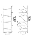
- An exemplary phase ramp of beam B 2 at splitter interface 322 is illustrated in FIG. 3 c as line 342 for a 45% reflectivity of coating 310 .
- beam B 3 also experiences a non-linear phase change from GT etalon 330 .
- ⁇ represents the phase change from the distance beam B 3 travels through beam splitter 302 from interface 322 to GT etalon 330 and back. Because beam splitter 302 is a cube, the distance beam B 3 travels through beam splitter 302 from interface 322 to GT etalon 330 and back is the same distance as beam B 2 . Therefore, the phase change resulting from traveling this distance, ⁇ , is the same as that for beam B 2 .
- An exemplary phase ramp of beam B 2 at splitter interface 320 is illustrated in FIG. 3 c as line 340 for a 4.5% reflectivity of coating 326 .
- beams B 2 and B 3 meet at the splitter interface, part of beam B 2 is reflected, while part of beam B 3 is passed through, thereby forming beam B 4 .
- FIG. 3 c at the frequencies where these two portions are substantially 180° (i.e. ⁇ ) out of phase, destructive interference occurs, while constructive interference occurs at the frequencies where these two portions are substantially in phase.
- This spectral response is illustrated in FIG. 3 b as line 332 .
- beam B 1 comprises a set of channels (f 2 , f 3 , f 4 , f 5 and f 6 as illustrated)
- this spectral response results in beam B 4 carrying a first sub-set of the channels, i.e. f 2 , f 4 and f 6 , which, for example, correspond to even ITU channels.
- This spectral response is illustrated in FIG. 3 b as line 334 .
- beam B 1 comprises a set of channels (f 2 , f 3 , f 4 , f 5 and f 6 as illustrated)
- this spectral response results in beam B 5 carrying a second sub-set of channels, i.e. f 3 and f 5 , which, for example, correspond to odd ITU channels.
- the shape of the spectral responses of interferometer 300 is determined by the reflectivity of coatings 310 and 326 .
- the phases of each beam are more closely matched in each passband.
- the phase difference between each beam is closer to ⁇ during each stop-band. This results in a spectral response, which has a wider pass band and steeper roll-off at the band edge when compared to an MGTI with equivalent FSR int .
- FIG. 4 lines 400 represent spectral responses for the present invention with a reflectivity ratio of 10:1 for a number of RI reflectivities between 44-50%.
- Line 402 represents the spectral response for an MGTI with a GT etalon having a front reflectivity of 15%.
- FIG. 5 a illustrates another embodiment of an interferometer 500 according to the principles of the present invention in which the two etalons are slightly de-phased from one another so as to reduce chromatic dispersion.
- interferometer 500 is similar to interferometer 300 , i.e. two almost identical GT etalons, 520 and 530 , (with cavity length of d) are initially placed on adjacent sides of a beamsplitter 502 , in a Michelson interferometer configuration with an effective optical path difference of a length L between them.
- the etalon 530 includes a front plate 524 with a partially reflective coating 526 , and a back plate 504 with an almost fully reflective coating 506 .
- the front and back plates 524 and 504 are separated by spacers 507 , which are preferably made from a ULE material.
- etalon 520 includes a back plate 514 with a reflective coating 512 , and a front plate 508 with a reflective coating 510 .
- the two plates 514 and 508 are held apart by ULE spaces 511 .
- interferometer 500 acts to deinterleave channels when a beam B 1 comprising a set of channels, for example, ITU even and odd channels is input.
- the spectral response of beam B 4 results in beam B 4 carrying a first sub-set of channels, for example, even ITU channels
- the spectral response of beam B 5 results in beam B 5 carrying a second sub-set of channels, for example, odd ITU channels.
- interferometer 500 acts to interleave channels when both beam B 4 carrying a first sub-set of channels (e.g., even ITU channels) and beam B 5 carrying a second sub-set of channels (e.g. odd ITU channels) are input to interferometer 500 .
- beam B 1 is output carrying the set of channels (e.g., the even and odd ITU channels).
- the GT etalons 530 and 520 are slightly de-phased from one another such that the positive dispersion slope of one is aligned with the negative dispersion slope of the other.
- This is preferably achieved by changing the effective cavity length of one of the GT etalons by a length ⁇ to shift the resonance peak of the GT etalon.
- the effective resonance peak is shifted by 1 ⁇ 2 (or an odd multiple thereof) of the etalon free spectral range (FSR GT ) in order to achieve minimal dispersion. This corresponds to approximately a ⁇ /4 shift in the cavity length, i.e.
- One method of changing the effective cavity length of one of the GT etalons is by physically changing the cavity length of the GT etalon by the length ⁇ . This is illustrated in FIG. 5 a by GT etalon 530 having a physical cavity length of d+ ⁇ . It will be appreciated by one of skill in the art, however, that there are other possible methods of changing the effective cavity length of one of the GT etalons.
- FIG. 5 b illustrates how the dispersion profiles from GT etalons 520 and 530 align when there is an approximately a ⁇ /4 shift in the cavity length of GT etalon 530 .
- Line 540 is the dispersion profile resulting from GT etalon 530
- line 542 is the dispersion profile resulting from GT etalon 520 .
- the resulting, minimal dispersion profile per wavelength is shown as line 544 .
- the resulting effective dispersion appears to mimic the average dispersion and under these circumstances the overall dispersion is reduced.
- the effective optical path difference becomes L+ ⁇ . Therefore, in the preferred embodiment in which there is an approximately ⁇ /4 shift in the effective cavity length (d ⁇ /4), the shift from L to acquire the optimal phase response is ⁇ /4. As such, the preferable length of the effective optical path difference is shifted from L to L ⁇ /4. Please note, if ⁇ is a positive shift in length d, then it will be a positive shift in length L. The same is true for a negative shift.
- the level of dispersion oscillates from a low dispersion where there is an interleaved output to a high dispersion where the interleaver output is destroyed. This occurs as the two dispersion slopes from GT etalons 520 and 530 are effectively added or subtracted depending on the optical phase difference.
- interferometer 500 with a variable effective cavity length of etalon 530 and variable effective optical path difference, a tunable dispersion compensator is provided.
- GT etalons 520 and 530 are weak, i.e. ⁇ 10%, and more preferably ⁇ 5%, so that the effective dispersion averaging (cancellation) is achieved over an extended wavelength.
- the reflectivities of coatings 526 and 510 are approximately 2%, but higher or lower reflectivies can be used.
- GT etalons 520 and 530 can have different reflectivities of coatings 526 and 510 , e.g. coating 526 with a reflectivity eof 2% and coating 510 with a reflectivity of 4%.
- Typical values obtainable for the embodiment of FIG. 5 a with a reflectivity of 2.2% for coatings 526 and 510 are as follows: 50 GHz Channel 25 GHz Channel Spacing Spacing MAX. DISPERSION +/ ⁇ 30 ps/nm +/ ⁇ 120 ps/nm BANDWIDTH @ 40.6 GHz 20.2 GHz 1 dB CROSSTALK >25 dB >22 dB
- FIG. 5 c Illustrated in FIG. 5 c is an exemplary spectral response for interferometer 500 designed as a 25 GHz interleaver with a reflectivity of 99.7% for coatings 506 and 512 , and a reflectivity of 2.5% for coatings 510 and 526 .
- Line 546 illustrates the spectral response for beam B 4
- line 548 illustrates the spectral response for beam B 5 .
- the effective optical path difference is L+ ⁇ /4; however, some re-phasing of the effective optical path difference may be able to further optimize this profile.
- FIG. 5 d illustrates the resulting dispersion profile per wavelength for the interleaver designed as a 25 GHz interleaver. As can be seen from FIG. 5 d , the overall dispersion magnitude for the interleaver according to the present invention is effectively reduced by a factor of 7 to 10, as compared to the conventional 25 GHz interleaver.
- FIGS. 6 a to 6 d illustrate polarization-based implementations of the present invention.
- interferometer 600 comprises a polarization dependent delay section 609 and a modified GT etalon 610 with a physical cavity length d.
- Interferometer 600 acts to deinterleave channels when an optical beam 601 comprising a set of channels, for example, ITU even and odd channels is input via a port 602 .
- the optical beam 601 can be launched linearly polarized or, as in the illustrated embodiment, be split into two orthogonally polarized optical beams 601 a and 601 b (not shown) by a walk-off crystal 603 , one of which passes through a half wave plate 604 , thereby forming two like-polarized sub-beams.
- the like polarized sub-beams 601 a and 601 b pass directly through a first polarization beam splitter (PBS) 605 , a non-reciprocal rotator 606 , and a second polarization beam splitter 607 without being affected.
- a quarter wave plate 608 rotates the polarization of both sub-beams 601 a and 601 b by 45° before entry into the delay section 609 .
- the non-reciprocal rotator 606 is preferably comprised by a Faraday rotator and a quarter wave plate, which are designed to rotate the polarization of beams traveling in one direction by 90°, while having no cumulative effect on the polarization of beams traveling in the opposite direction.
- the delay section 609 introduces an effective optical path difference between the s and p components in each of the sub-beams 601 a and 601 b , similar to the effective optical path difference introduced in interleaver 500 .
- Delay section 609 is preferably made from two birefringent crystals 611 and 612 whose materials (e.g. TiO 2 crystals and YVO 4 crystals) are chosen to improve the thermal stability of delay section 609 over a selected temperature range. It is within the spirit of the present invention, however, to use a single birefringent crystal, or more than two crystals whose materials are chosen to make delay section 609 temperature insensitive.
- delay section 609 is made from birefringent material, when two linearly polarized optical beams that have different planes of polarization pass therethrough, one of the beams travels at a faster velocity than the other. Therefore, the s and p components of the optical beams 601 a and 601 b experience an effective optical path difference when they pass through delay section 609 .
- the effective optical path difference is preferably designed to be approximately L+ ⁇ , where L is equal to one-half the cavity length d.
- the length of the delay section 609 may additionally be made variable so as to provide for an adjustable effective optical path difference.
- the modified GT etalon 610 comprises a front plate 615 with a partially reflective (e.g. 2%) coating 616 , spacers 617 a and 617 b (preferably made from ultra low expansion material (ULE)), a quarter waveplate 618 , and a back plate 619 with a highly reflective (near 100%) coating 620 .
- interferometer 600 operates similarly to interferometer 500 by de-phasing the operation of modified GT etalon 610 on the s and p components of the sub-beams 601 a and 601 b , such that the positive dispersion slope for its operation on the s components is aligned with the negative dispersion slope for its operation on the p components.
- the effective resonance peak is preferably shifted by about 1 ⁇ 2 of the etalon's free spectral range (FSR GT ) to achieve minimal dispersion. This corresponds to approximately a ⁇ /4 difference between the effective cavity lengths experienced by the s and p components of the sub-beams 601 a and 601 b .
- waveplate 618 is preferably a quarter-waveplate with its optical axis at 450 to the polarization planes of the sub-beams 601 a and 601 b .
- sub-sub-beams 621 a and 621 b each containing a part of one set of channels, are reflected toward a walk-off crystal 622 .
- a waveplate 623 rotates the polarization of one of the sub-sub-beams 621 a or 621 b , so that the two sub-sub-beams can be combined in the walk-off crystal 622 for output lens 624 and waveguide 625 .
- sub-sub-beams 626 a and 626 b pass through the PBS 607 , and have their polarizations rotated by 90° in the non-reciprocal rotator 606 . Accordingly, the sub-sub-beams 626 a and 626 b are reflected by the PBS 605 towards a walk-off crystal 627 .
- a waveplate 628 rotates the polarization of one of the sub-sub-beams 626 a or 626 b , so that the two sub-sub-beams can be combined in the walk-off crystal 627 for output lens 628 and waveguide 629 .
- FIGS. 6 c and 6 d illustrate alternate embodiments of the phase shifting section 609 , wherein the beam is physically separated into s and p components by a polarization beam splitter, such as a PBS cube 630 (FIG. 6 c ) or a walk-off crystal 635 (FIG. 6 d ).
- a polarization beam splitter such as a PBS cube 630 (FIG. 6 c ) or a walk-off crystal 635 (FIG. 6 d ).
- a delay section 640 which has an index of refraction that is different than air. Accordingly, when the sub-beams are recombined by a second PBS cube 645 or walk-off crystal 650 , a phase shift has been introduced therebetween.
- FIG. 7 a illustrates an alternate manner of injecting input optical beam
- FIG. 8 illustrates an alternate configuration
- FIG. 7 a illustrates an alternate manner of injecting optical beams that allows for a four-port device.
- An interferometer 700 is constructed according to the principles of either the interferometer of FIG. 3 a or the interferometer of FIG. 5 a , i.e. the path difference is either L of L+ ⁇ , and the cavity length of etalon 730 is either 2L or 2L+ ⁇ .
- the path difference is either L of L+ ⁇
- the cavity length of etalon 730 is either 2L or 2L+ ⁇ .
- optical beams are injected at an angle to the normal.
- each of the resulting beams are directed towards their respective GT etalon also at an angle to the normal of the respective GT etalon. This results in the reflected beams intersecting at a point along splitter interface 722 that is different than the point at which the optical beam was split.
- an optical beam when an optical beam is injected as beam B 1 as shown, it is split into a beam B 3 directed towards GT etalon 730 at an angle to the normal and a beam B 2 directed towards GT etalon 720 at an angle to the normal.
- beam B 3 and beam B 2 are reflected back as beams B 7 and B 8 , respectively, beams B 7 and B 8 intersect at splitter interface 722 and combine to create beams B 5 and B 4 as outputs.
- an optical beam when an optical beam is injected as beam B 5 , it is split into a beam B 7 directed towards GT etalon 730 at an angle to the normal and a beam B 8 directed towards GT etalon 720 at an angle to the normal.
- beams B 3 and B 2 intersect at splitter interface 722 and combine to create beams B 1 and B 6 as outputs.
- an optical beam can be input as either beam B 4 and B 6 .
- an optical beam is input as beam B 4 , it is split into a beam B 7 directed towards GT etalon 730 at an angle to the normal and a beam B 8 directed towards GT etalon 720 at an angle to the normal.
- beam B 7 and beam B 8 are reflected back as beams B 3 and B 2 , respectively, beams B 3 and B 2 intersect at splitter interface 722 and combine to create beams B 1 and B 6 as outputs.
- beam B 6 When an optical beam is injected as beam B 6 , it is split into a beam B 3 directed towards GT etalon 730 at an angle to the normal and a beam B 2 directed towards GT etalon 720 at an angle to the normal.
- beam B 3 and beam B 2 are reflected back as beams B 7 and B 8 , respectively, beams B 7 and B 8 intersect at splitter interface 722 and combine to create beams B 5 and B 4 as outputs.
- FIG. 7 b illustrates a polarization dependent version of the angled incidence embodiment of FIG. 7 a .
- Delay sections 740 and 745 are added to provide a relative delay of L or L+ ⁇ between the s and p components of the split beams B 2 and B 3 , respectively.
- waveplates 750 and 755 are included to provide the additional ⁇ /4 delay.
- FIG. 8 illustrates an alternate construction of interferometer 300 or interferometer 500 using a plate beam splitter 802 .
- a GT etalon 820 is constructed similar to GT etalon 320 or GT etalon 520 and is coupled to plate beam splitter 802 .
- GT etalon 830 is constructed similar to GT etalon 330 or GT etalon 530 and is coupled to plate beam splitter 802 .
- GT etalons 820 and 830 are coupled to plate beam splitter with an appropriate optical path difference.
- beam B 1 when an optical beam B 1 is injected at an angle to the normal of plate beamsplitter 802 , beam B 1 is split into a beam B 3 directed towards GT etalon 830 at an angle to the normal and a beam B 2 directed towards GT etalon 820 at an angle to the normal.
- beam B 3 and beam B 2 are reflected back as beams B 7 and B 8 , respectively, beams B 7 and B 8 intersect at splitter interface 822 and combine to create beams B 5 and B 4 as outputs.
- FIG. 8 b the GT etalons 820 and 830 , illustrated in FIG. 8 a , are replaced by ring resonators 850 and 860 .
- the ring resonator 840 includes a front body 870 with a partially reflective surface 872 , and two angled mirrors 875 .
- the ring resonator 860 includes a front body 880 with a partially reflective surface 882 , and two angled mirrors 885 . Any number of angled mirrors can be used to form the ring resonator, as known in the industry.
- the front body 880 has an index of refraction different than the remainder of the optical path, and is wider than the front body 870 , thereby creating an optical path length difference of L or L+ ⁇ as hereinbefore described.
- Tuning plates 890 are provided in the ring resonators 850 and 860 to enable the cavity length thereof to be tuned to 2L or 2L+ ⁇ as hereinbefore described.
- both cavities 850 and 860 also include a birefringent element, e.g. by replacing the tuning plates by waveplates 890 , for creating an additional cavity length difference of ⁇ /4 for the two orthogonal components, as hereinbefore described.
- a single resonator device as in FIGS. 6 a and 6 b , can also be constructed by using only one ring resonator 850 .
- FIG. 9 illustrates an embodiment to create two de-phased GT etalons using the fact that the resonance peak of a GT etalon changes as the angle of the incident beam is varied.
- a polarizing beam splitter 900 such as a Wallaston prism, splits an input beam B 1 into linearly polarized beams B 2 and B 3 have an angle therebetween. Both beams B 2 and B 3 are directed towards a GT etalon 902 with a cavity length d designed to be operable on the desired channel spacing. Beams B 2 and B 3 have different incidence angles because of the angle therebetween.
- FIG. 5 a provides for reduced dispersion.
- the dispersion magnitudes are ⁇ 100 ps/nm.
- this amount of dispersion is not acceptable.
- FIGS. 10 a , 11 a and 12 a illustrate embodiments to further reduce the chromatic dispersion produced by interferometer 500 of FIG. 5 a .
- the basis for all three embodiments is to provide a means for producing complementary dispersion profiles for compensating the interferometer's original dispersion profiles.
- the complementary dispersion profiles have similar periodicity and amplitudes as the original, but the compensating profiles have been shifted so that the positive slopes of one profile are aligned with the negative slopes of the other profile. Accordingly, overall dispersion is greatly reduced.
- FIG. 10 a illustrates an embodiment to further reduce the chromatic dispersion in the embodiment of FIG. 5 a by cascading the interferometer of FIG. 5 with a second similar interferometer.
- an interferometer 1000 like interferometer 500 has a second interferometer 1002 , similar to interferometer 1000 , placed in cascade for one of interferometer 1000 's outputs and a third interferometer 1004 , also similar to interferometer 1000 , placed in cascade for interferometer 1000 's other output.
- a first subset of channels (e.g. even ITU channels) is output as beam B 2 to interferometer 1002 with some remaining dispersion
- a second subset of channels (e.g. odd ITU channels) is output as beam B 3 to interferometer 1004 , also with some remaining dispersion.
- the interferometer 1002 compensates for this remaining dispersion in beam B 2 and outputs the first subset of channels with a further reduced dispersion profile.
- the interferometer 1004 compensates for the remaining dispersion in beam B 2 and outputs the second subset of channels with a further reduced dispersion profile 1030 .
- interferometer 1000 has the effective cavity length of GT etalon 1006 shifted by ⁇ /4 (i.e. d+ ⁇ /4) and the effective optical path difference is also shifted by ⁇ /4 (i.e. L+ ⁇ /4). This reduces the chromatic dispersion of interferometer 1000 .
- the remaining dispersion of interferometer 1000 has a quasi-periodic structure with a period of half of the channel spacing.
- An exemplary dispersion profile for interferometer 1000 is illustrated as line 1020 in FIG. 10 b.
- interferometer 1002 and interferometer 1004 can compensate for it when they have an additional effective cavity shift and an extra effective optical path difference.
- the additional effective cavity shift and an extra effective optical path difference shifts the dispersion profiles of interferometers 1002 and 1004 to compensate for the remaining dispersion of interferometer 1000 .
- Interferometer 1002 and interferometer 1004 preferably have an additional effective cavity shift of a quarter of a channel's spacing and an extra effective optical path difference of a half of a channel's spacing. Therefore, it is preferable for interferometer 1002 to have a GT etalon 1012 which has an additional ⁇ /8 shift (i.e.
- interferometer 1004 it is preferable for interferometer 1004 to have a GT etalon 1014 which has an additional ⁇ /8 shift (i.e. d+ ⁇ /4+ ⁇ /8) in the effective cavity length and an additional shift in the effective optical path difference between the two GT etalons 1014 and 1016 of ⁇ /16 (i.e. L+ ⁇ /4+ ⁇ /16).
- interferometer 1002 and interferometer 1004 each produce a shifted dispersion profile as described above. This is illustrated by line 1022 in FIG. 10 b .
- the shifted dispersion profile 1022 compensates for the dispersion profile 1020 , which produces a reduced dispersion profile 1030 as illustrated in FIG. 10 c.
- FIG. 10 d illustrates an exemplary passband 1040 of interleaver 1000 for a single channel and an exemplary passband 1042 of interferometer 1002 or 1004 for the same channel.
- the additional effective cavity shift and an extra effective optical path difference in interferometer 1002 or interferometer 1004 also cause a shift in the center frequency of passband 1042 relative to passband 1040 .
- the average passband is indicated by line 1046 .
- the resultant cascaded passband 1048 has higher isolation, i.e. steeper sides, but a reduced flat passband width. While the flat passband is reduced, the cascaded arrangement improves the isolation, which provides the ability to find better compromises in terms of bandwidth vs. isolation for individual devices.
- Typical values obtainable for the embodiment of FIG. 10 a with a reflectivity of 2.2% for the partially reflective coatings of the GT etalons are as follows: 50 GHz Channel 25 GHz Channel Spacing Spacing MAX. DISPERSION +/ ⁇ 6 ps/nm +/ ⁇ 23 ps/nm BANDWIDTH @ 28 GHz 14 GHz 1 dB CROSSTALK >35 dB >30 dB
- FIG. 11 a conceptually illustrates another embodiment to further reduce the chromatic dispersion in the embodiment of FIG. 5 a .
- This embodiment is similar to that of FIG. 5 except that the beams B 2 and B 3 are multi-passed two or more times through respective GT etalons 1120 and 1130 .
- the beams B 2 and B 3 are multi-passed two or more times through respective GT etalons 1120 and 1130 .
- the reflectivity of the front plates 1124 and 1108 needs to be reduced to give the same interleaver output.
- the level of reflectivity for front plates 1124 and 1108 is reduced, the sensitivity to the actual level of reflectivity increases. For instance, if the reflectivity of front plates 1124 and 1108 varies by more than 0.1% for a quadruple pass of beams B 2 and B 3 , significant changes in the profile may be observed.
- FIGS. 11 b and 11 c illustrate spectral responses and chromatic dispersion profiles for a double pass and quadruple pass respectively.
- the reflectivity of front plates 1124 and 1108 is 0.7%, while for the quadruple pass the reflectivity is lowered to 0.2%.
- the residual dispersion is reduced to ⁇ 70 ps/nm and the cancellation effect also becomes more effective because of the matching of the dispersion slopes and linearity.
- FIG. 11 c for a quadruple pass with front reflectivity's of 0.2%, the dispersion is further reduced to 35 ps/nm.
- FIG. 1 d illustrates one embodiment for multi-passing beams B 2 and B 3 through respective GT etalons based on polarization.
- a linear polarized optical beam B 1 is incident on a polarization beam splitter cube 1102 .
- Optical beam B 1 has a polarization orientation that is 45° to the effective fast axis of polarization beam splitter cube 1102 . This causes beam B 1 to be split into two linearly polarized beams B 1 3 and B 1 2 with orthogonal polarizations.
- Beam B 1 3 is directed towards GT etalon 1120
- beam B 1 2 is directed towards GT etalon 1130 .
- Beams B 1 3 and B 1 2 pass through quarter waveplates 1106 and 1107 , respectively, which causes beams B 1 3 and B 1 2 to become circularly polarized beams. On being reflected from each arm they re-pass through the corresponding quarter waveplate, which now causes beams B 1 3 and B 1 2 to become linear polarized light with a polarization orientation orthogonal to their original orientations. Therefore, reflected beam B 1 3 is reflected at splitter interface 1122 , while beam B 1 2 is transmitted through at splitter interface 1122 .
- beams B 1 3 and B 1 2 being directed towards rooftop reflector 1104 after combining at splitter interface 1122 .
- Rooftop reflector 1104 directs the combined beams B 1 3 and B 1 2 back to splitter interface 1122 , where beam B 1 3 is again directed towards GT etalon 1120 as beam B 2 3 and beam B 1 2 is again directed towards GT etalon 1130 as beam B 2 2.
- Beams B 2 2 and B 2 3 again pass through the respective GT etalons 1130 and 1120 and return to splitter interface 1122 .
- the effective optical path difference between the arms is made to be L + ⁇ 2
- Beams B 2 2 and B 2 3 are recombined at splitter interface and output as beam B 4 .
- An additional polarization beam splitter (not shown) is used to separate one set of channels from the other set of orthogonally polarized channels.
- FIG. 12 a illustrates another embodiment to further reduce the chromatic dispersion in the embodiment of FIG. 5 a .
- multi-cavity GT etalons 1220 and 1230 are used in the arms of the Michelson interferometer configuration with an effective optical path difference between the arms.
- multi-cavity GT etalons 1220 and 1230 have multiple cavities of cavity length d chosen to operate on predetermined channel spacing, e.g. 25 GHz.
- a back cavity 1240 of the multi-cavity GT etalon 1230 is similar to the cavity of GT etalon 530 and is formed from a back plate 1204 with a highly reflective (near 100%) coating 1206 and a wedge shaped intermediate plate 1224 having a partially reflective coating 1226 .
- a forward cavity 1222 of the GT etalon 1230 is formed from a front plate 1236 with a coating 1238 , providing very low reflectivity, and the intermediate plate 1224 .
- a back cavity 1242 of multi-cavity GT etalon 1220 is similar to the cavity of GT etalon 520 , and is formed from a back plate 1214 , with a highly reflective (near 100%) coating 1212 , and a wedge shaped intermediate plate 1208 having a partially reflective coating 1210 .
- a forward cavity 1232 of the GT etalon 1220 is formed from a front plate 1234 , with a coating 1244 providing very low reflectivity, and the intermediate plate 1208 .
- Preferable reflectivities are 99.5% for back coatings 1206 and 1212 , 2.2% for intermediate coatings 1210 and 1226 , and ⁇ 39 dB for front coatings 1240 and 1238 (corresponding to about 0.013%).
- the intermediate plates 1208 and 1224 are in the shape of wedges to prevent any back reflections from the front surfaces thereof from affecting the function of the forward resonant cavities 1222 and 1232 .
- GT etalons 1230 and 1220 are slightly de-phased from one another such that the positive dispersion slope of one is aligned with the negative dispersion slope of the other. This is preferably achieved by changing the effective cavity length of each of the cavities of GT etalon 1230 by a length ⁇ .
- the length ⁇ corresponds to approximately a ⁇ /4 shift in the cavity length.
- the arms of the interferometer configuration have an optical path difference, L, between them, which is preferably equal to one-half the cavity length d.
- the optical path difference L is also adjusted by ⁇ .
- interferometer 1200 acts to deinterleave channels when a beam B 1 comprising a set of channels, for example, ITU even and odd channels is input.
- the spectral response of beam B 4 results in beam B 4 carrying a first sub-set of channels, for example, even ITU channels
- the spectral response of beam B 5 results in beam B 5 carrying a second sub-set of channels, for example, odd ITU channels.
- interferometer 1200 acts to interleave channels when both beam B 4 carrying a first sub-set of channels (e.g., even ITU channels) and beam B 5 carrying a second sub-set of channels (e.g. odd ITU channels) are input to interleaver 1200 .
- beam B 1 is output carrying the set of channels (e.g., the even and odd ITU channels).
- FIG. 12 b is a schematic representation of a solid version of the multi-cavity etalon embodiment of FIG. 12 a , in which solid transparent blocks 1250 , 1251 , 1252 and 1253 with the appropriate coatings 1206 , 1226 , 1238 , 1244 , 1210 and 1212 thereon, define the resonant cavities.
- the blocks 1250 and 1251 are slightly longer (i.e. by ⁇ ) than the blocks 1252 and 1253 , for reasons that have been hereinbefore discussed.
- the beamsplitter 1260 is comprised of a triangular section 1262 and a trapezoidal section 1264 with a ⁇ fraction (50/50) ⁇ coating 1266 positioned therebetween.
- the trapezoidal section 1264 has the optical path length difference (i.e. L or L+ ⁇ ) built right in.
- interferometer 1200 has a similar spectral response as interleaver 500 .
- interferometer 1200 has a lower dispersion (line 1275 ) resulting from the forward resonant cavities 1222 and 1232 with the very low front reflectivity canceling the dispersion from the back cavities 1240 and 1242 , respectively.
- the dispersion from one of the forward cavities is represented by line 1280
- the dispersion from one of the back cavities is represented by line 1285 .
- FIGS. 12 e and 12 f illustrate polarization dependent versions of the multi-cavity GT embodiments.
- the embodiment disclosed in FIG. 12 e is similar to the embodiment of FIG. 12 a , with the addition of an optical path delay section 1250 in each arm, and a quarter wave plate 1260 in each cavity.
- the embodiment disclosed in FIG. 12 f is similar to the embodiment of FIG. 6 b , except that the single cavity GT etalon 600 is replace by a multi-cavity etalon 1290 .
- the multi-cavity etalon 1290 includes a front cavity 1292 and a rear cavity 1294 , which are defined by reflective surfaces R 1 , R 2 , and R 3 .
- Another method of greatly reducing chromatic dispersion in the signals exiting the interferometer 500 is by including a dispersion compensator 590 in front of the interferometer 500 .
- the dispersion compensator 590 introduces an initial dispersion profile to the input signal B 1 that is complementary to the dispersion profile resulting from transmission through the interferometer 500 . Accordingly, the overall dispersion of the system will be greatly reduced.
- the dispersion compensator 590 may comprise a GT etalon with the same FSR as the etalons 520 and 530 ; however, the optimum reflectivity of the front partially reflective surface of this GT etalon would be the same as that of the front reflective surfaces 1238 and 1244 of the multi-cavity etalon 1200 , i.e. ⁇ 39 dB or 0.013%.
- GT etalons can be assembled using solid or air-filled gaps.
- the dispersion compensator 590 comprises a Fabry-Perot (F-P) etalon with an FSR one half of the FSR of etalons 520 and 530 , e.g.
- the partially reflective surfaces of the F-P etalon of the dispersion compensator 590 should also be 2.2% to provide a dispersion profile that is complementary to that of the interferometer 500 , i.e. shifted enough so that the positive dispersion slopes of one profile line up with the negative dispersions slopes of the other.
- FIG. 12 g illustrates a hybrid version of the present invention with a multi-cavity etalon 1230 ′ (see FIG. 12 a ) in one arm and a single cavity etalon 520 ′ (see FIG. 5 a ) in the other arm.
- the arm with the single cavity etalon 520 ′ includes the L+ ⁇ delay line.
- the single cavity etalon 520 ′ has a front reflective coating 510 ′, which preferably ranges between 0% and 2%, and a rear reflective coating 512 ′, which preferably is close to 100%.
- the multi-cavity etalon 1230 ′ has a front reflective coating 1238 ′, which preferably ranges between 0% and 2%, an intermediate reflective coating 1226 ′, which preferably ranges between 20% and 50%, and a rear reflective coating 1206 ′, which preferably is close to 100%.
- the front cavity 1222 ′ is offset by A from the rear cavity 1240 ′.
- FIGS. 12 h and 12 i represent typical spectral responses for the interleaver of FIG. 12 g .
- both front reflective coatings 510 ′ and 1238 ′ have a reflectivity of 0.8%
- the intermediate reflective coating 1226 ′ has a reflectivity of 35%
- both rear reflective coatings have a reflectivity of 99.99%.
- both front reflective coatings 510 ′ and 1238 ′ have a reflectivity of 0.1%
- the intermediate reflective coating 1226 ′ has a reflectivity of 35%
- both rear reflective coatings have a reflectivity of 99.99%.
- FIG. 13 a illustrates the SEI version of the invention, in which a single etalon 1300 includes front and rear plates 1305 and 1310 with low reflectivity coatings, e.g. 2.2%.
- An input waveguide 1325 launches an input signal into the etalon 1300 , while a first output waveguide 1330 collects the reflected light and a second output waveguide 1335 collects the transmitted light.
- One of the output waveguides e.g.
- the modified SEI interleaver described above provides a flat top interleaver with low dispersion in the pass band (i.e. ⁇ 30 ps/nm).
- FIG. 13 b illustrates a multi-cavity version of the SEI, in which the etalon 1300 is replaced by a multi-cavity etalon 1375 including a first cavity 1380 , a second cavity 1385 , and a third cavity 1390 .
- a micro-optics version of the SEI interleaver is illustrated in FIG. 14. Instead of waveguides the transmitted and reflected fields travel through free space.
- a mirror 1410 reflects the reflected light from an etalon 1400 (single of multi-cavity) to a ⁇ fraction (50/50) ⁇ beam splitter/combiner 1415 , while a mirror 1420 reflects the transmitted light thereto.
- the mirror 1420 is recessed to provide the ⁇ /4 path length difference.
- a mirror 1425 directs the reflected light from the beam splitter/combiner 1415 back towards the beam splitter/combiner 1415 for recombining, while a mirror 1430 directs the transmitted light from the beam splitter/combiner 1415 back towards the beam splitter/combiner for recombining.
- the mirror 1430 is recessed to provide a path length difference of L. After recombination, the light containing a first set of channels, e.g. the odd ITU channels, is output a first output port 1435 , while the light containing a second set of channels, e.g. the even ITU channels, is output a second output port 1440 .
- FIG. 15 illustrates an alternative version of an SEI interleaver of FIG. 13, in which a ring resonator 1500 replaces the etalon 1300 .
- a multi-ring resonator can replace the single ring resonator 1500 .
Priority Applications (4)
| Application Number | Priority Date | Filing Date | Title |
|---|---|---|---|
| US10/058,534 US6683721B2 (en) | 2001-02-27 | 2002-01-28 | Low dispersion interleaver |
| EP02251219A EP1235086A3 (en) | 2001-02-27 | 2002-02-22 | Low dispersion interleaver |
| CA002372906A CA2372906A1 (en) | 2001-02-27 | 2002-02-22 | Low dispersion interleaver |
| CNB021237115A CN1305241C (zh) | 2001-02-27 | 2002-02-27 | 低色散交织器 |
Applications Claiming Priority (3)
| Application Number | Priority Date | Filing Date | Title |
|---|---|---|---|
| US27142801P | 2001-02-27 | 2001-02-27 | |
| US29398501P | 2001-05-30 | 2001-05-30 | |
| US10/058,534 US6683721B2 (en) | 2001-02-27 | 2002-01-28 | Low dispersion interleaver |
Publications (2)
| Publication Number | Publication Date |
|---|---|
| US20020171908A1 true US20020171908A1 (en) | 2002-11-21 |
| US6683721B2 US6683721B2 (en) | 2004-01-27 |
Family
ID=27369467
Family Applications (1)
| Application Number | Title | Priority Date | Filing Date |
|---|---|---|---|
| US10/058,534 Expired - Fee Related US6683721B2 (en) | 2001-02-27 | 2002-01-28 | Low dispersion interleaver |
Country Status (4)
Cited By (12)
| Publication number | Priority date | Publication date | Assignee | Title |
|---|---|---|---|---|
| US20030035212A1 (en) * | 2001-08-08 | 2003-02-20 | Accumux Technologies, Inc. | Athermal birefringent optical interleavers with flat-top passbands |
| US6643063B2 (en) * | 2001-11-14 | 2003-11-04 | Oplink Communications, Inc. | Deinterleaver with high isolation and dispersion compensation and 50/200GHz interleaver and deinterleaver |
| US6785000B2 (en) * | 2002-06-24 | 2004-08-31 | Jds Uniphase Corporation | Bulk optical interferometer |
| US20050270544A1 (en) * | 2004-06-04 | 2005-12-08 | Optoplex Corporation | Variable dispersion step-phase interferometers |
| US20090162066A1 (en) * | 2007-12-19 | 2009-06-25 | Nec Laboratories America, Inc. | Intra-Channel Equalizing Optical Interleaver |
| US20170261669A1 (en) * | 2014-11-29 | 2017-09-14 | Huawei Technologies Co., Ltd. | Phase retarder and optical comb filter thereof |
| US11159245B2 (en) * | 2019-07-03 | 2021-10-26 | Raytheon Company | Methods and apparatus for cavity angle tuning for operating condition optimization |
| US11290191B2 (en) | 2019-06-20 | 2022-03-29 | Raytheon Company | Methods and apparatus for tracking moving objects using symmetric phase change detection |
| US11303356B1 (en) | 2019-04-18 | 2022-04-12 | Raytheon Company | Methods and apparatus for maintaining receiver operating point with changing angle-of-arrival of a received signal |
| US11307395B2 (en) | 2019-05-23 | 2022-04-19 | Raytheon Company | Methods and apparatus for optical path length equalization in an optical cavity |
| US11353774B2 (en) * | 2019-07-15 | 2022-06-07 | Raytheon Company | Methods and apparatus for cavity length tuning for operating point optimization |
| US20230106876A1 (en) * | 2021-10-01 | 2023-04-06 | Lumentum Operations Llc | Bidirectional filter |
Families Citing this family (20)
| Publication number | Priority date | Publication date | Assignee | Title |
|---|---|---|---|---|
| US6519065B1 (en) * | 1999-11-05 | 2003-02-11 | Jds Fitel Inc. | Chromatic dispersion compensation device |
| WO2002067025A1 (fr) * | 2001-02-20 | 2002-08-29 | Sumitomo Osaka Cement Co., Ltd. | Résonateur optique et module de commande de longueur d'ondes utilisant ce résonateur |
| US6690846B2 (en) * | 2001-03-01 | 2004-02-10 | Chorum Technologies Lp | Dispersion-compensated optical wavelength router |
| AU2002345868A1 (en) * | 2001-06-25 | 2003-01-08 | Massachussets Institute Of Technology | Tunable chromatic dispersion compensation |
| US7158697B2 (en) * | 2002-04-29 | 2007-01-02 | Avanex Corporation | Optical multiplexer and demultiplexer apparatus utilizing multiple polarization beam splitters and reflection interferometers |
| WO2003096091A1 (en) * | 2002-05-07 | 2003-11-20 | Engana Pty Ltd | Narrowband filter method and apparatus |
| GB0210899D0 (en) * | 2002-05-13 | 2002-06-19 | Aston Photonic Tech Ltd | Dispersion compensator |
| US6992823B2 (en) * | 2002-06-24 | 2006-01-31 | Oplink Communications, Inc. | Chromatic dispersion compensator |
| US7061946B2 (en) * | 2002-11-13 | 2006-06-13 | Intel Corporation | Intra-cavity etalon with asymmetric power transfer function |
| US7050671B1 (en) * | 2003-01-17 | 2006-05-23 | Jds Uniphase Corporation | Tunable compensation of chromatic dispersion using etalons with tunable optical path length and non-tunable reflectivity |
| US7023620B1 (en) | 2003-07-03 | 2006-04-04 | Research Electro-Optics, Inc. | Beam array pitch controller |
| US7616372B2 (en) * | 2006-04-06 | 2009-11-10 | Jds Uniphase Corporation | Piano MEMS with hidden hinge |
| US7433054B1 (en) * | 2006-05-18 | 2008-10-07 | Lockheed Martin Corporation | Tunable Michelson and Mach-Zehnder interferometers modified with Gires-Tournois interferometers |
| US20140226164A1 (en) * | 2012-11-27 | 2014-08-14 | Optoplex Corporation | Low-dispersion step-phase interferometer |
| US20140176956A1 (en) * | 2012-11-27 | 2014-06-26 | Optoplex Corporation | Super-Steep Step-Phase Interferometer |
| WO2017023384A2 (en) * | 2015-05-08 | 2017-02-09 | Massachusetts Institute Of Technology | Apparatus and methods for reconfigurable optical receivers |
| CN105929197A (zh) * | 2016-04-15 | 2016-09-07 | 中国科学院合肥物质科学研究院 | 一种非对称空间外差干涉测量风速的方法 |
| CN105974158A (zh) * | 2016-06-16 | 2016-09-28 | 中国科学院合肥物质科学研究院 | 一种非对称空间外差光谱仪风速测量标定装置及方法 |
| WO2019028943A1 (zh) * | 2017-08-08 | 2019-02-14 | 江苏弘开传感科技有限公司 | 一种微波谐振腔的腔长测量装置、传感器 |
| CN110441863A (zh) * | 2019-07-17 | 2019-11-12 | 福州腾景光电科技有限公司 | 一种超宽通带高容量滤波器 |
Citations (3)
| Publication number | Priority date | Publication date | Assignee | Title |
|---|---|---|---|---|
| US3611436A (en) * | 1969-01-24 | 1971-10-05 | Bell Telephone Labor Inc | Mode-selective laser using resonant prisms |
| US20020122614A1 (en) * | 2001-03-01 | 2002-09-05 | Gan Zhou | Dispersion-compensated optical wavelength router |
| US6559992B2 (en) * | 2000-03-27 | 2003-05-06 | Chorum Technologies Lp | Adjustable chromatic dispersion compensation |
Family Cites Families (7)
| Publication number | Priority date | Publication date | Assignee | Title |
|---|---|---|---|---|
| US6130971A (en) | 1998-08-06 | 2000-10-10 | Avanex Corporation | Fiber optic dense wavelength division multiplexer with a phase differential method of wavelength separation utilizing a polarization beam splitter and a nonlinear interferometer |
| JP2000231063A (ja) * | 1998-12-23 | 2000-08-22 | Jds Uniphase Inc | 光共振器を含む干渉計式光デバイス |
| US6281977B1 (en) | 1998-12-23 | 2001-08-28 | Jds Fitel Inc. | Interferometric optical device including an optical resonator |
| CA2256963A1 (en) | 1998-12-23 | 2000-06-23 | Nigel Copner | Three port resonant optical cavity |
| US6252716B1 (en) | 1999-07-22 | 2001-06-26 | Jds Uniphase Photonics C.V. | Bulk optic interleaver |
| US6169604B1 (en) | 1999-02-10 | 2001-01-02 | Avanex Corporation | Nonlinear interferometer for fiber optic dense wavelength division multiplexer utilizing a phase bias element to separate wavelengths in an optical signal |
| US6169626B1 (en) | 1999-06-29 | 2001-01-02 | E-Tek Dynamics | Optical signal interleaver |
-
2002
- 2002-01-28 US US10/058,534 patent/US6683721B2/en not_active Expired - Fee Related
- 2002-02-22 EP EP02251219A patent/EP1235086A3/en not_active Withdrawn
- 2002-02-22 CA CA002372906A patent/CA2372906A1/en not_active Abandoned
- 2002-02-27 CN CNB021237115A patent/CN1305241C/zh not_active Expired - Fee Related
Patent Citations (3)
| Publication number | Priority date | Publication date | Assignee | Title |
|---|---|---|---|---|
| US3611436A (en) * | 1969-01-24 | 1971-10-05 | Bell Telephone Labor Inc | Mode-selective laser using resonant prisms |
| US6559992B2 (en) * | 2000-03-27 | 2003-05-06 | Chorum Technologies Lp | Adjustable chromatic dispersion compensation |
| US20020122614A1 (en) * | 2001-03-01 | 2002-09-05 | Gan Zhou | Dispersion-compensated optical wavelength router |
Cited By (15)
| Publication number | Priority date | Publication date | Assignee | Title |
|---|---|---|---|---|
| US20030035212A1 (en) * | 2001-08-08 | 2003-02-20 | Accumux Technologies, Inc. | Athermal birefringent optical interleavers with flat-top passbands |
| US6982831B2 (en) * | 2001-08-08 | 2006-01-03 | Oplink Communications, Inc. | Athermal birefringent optical interleavers with flat-top passbands |
| US6643063B2 (en) * | 2001-11-14 | 2003-11-04 | Oplink Communications, Inc. | Deinterleaver with high isolation and dispersion compensation and 50/200GHz interleaver and deinterleaver |
| US6785000B2 (en) * | 2002-06-24 | 2004-08-31 | Jds Uniphase Corporation | Bulk optical interferometer |
| US20050270544A1 (en) * | 2004-06-04 | 2005-12-08 | Optoplex Corporation | Variable dispersion step-phase interferometers |
| US8064768B2 (en) * | 2007-12-19 | 2011-11-22 | Nec Laboratories America, Inc. | Intra-channel equalizing optical interleaver |
| US20090162066A1 (en) * | 2007-12-19 | 2009-06-25 | Nec Laboratories America, Inc. | Intra-Channel Equalizing Optical Interleaver |
| US20170261669A1 (en) * | 2014-11-29 | 2017-09-14 | Huawei Technologies Co., Ltd. | Phase retarder and optical comb filter thereof |
| US10866350B2 (en) * | 2014-11-29 | 2020-12-15 | Huawei Technologies Co., Ltd. | Phase retarder and optical comb filter thereof |
| US11303356B1 (en) | 2019-04-18 | 2022-04-12 | Raytheon Company | Methods and apparatus for maintaining receiver operating point with changing angle-of-arrival of a received signal |
| US11307395B2 (en) | 2019-05-23 | 2022-04-19 | Raytheon Company | Methods and apparatus for optical path length equalization in an optical cavity |
| US11290191B2 (en) | 2019-06-20 | 2022-03-29 | Raytheon Company | Methods and apparatus for tracking moving objects using symmetric phase change detection |
| US11159245B2 (en) * | 2019-07-03 | 2021-10-26 | Raytheon Company | Methods and apparatus for cavity angle tuning for operating condition optimization |
| US11353774B2 (en) * | 2019-07-15 | 2022-06-07 | Raytheon Company | Methods and apparatus for cavity length tuning for operating point optimization |
| US20230106876A1 (en) * | 2021-10-01 | 2023-04-06 | Lumentum Operations Llc | Bidirectional filter |
Also Published As
| Publication number | Publication date |
|---|---|
| EP1235086A3 (en) | 2004-02-18 |
| CN1407750A (zh) | 2003-04-02 |
| EP1235086A2 (en) | 2002-08-28 |
| CA2372906A1 (en) | 2002-08-27 |
| US6683721B2 (en) | 2004-01-27 |
| CN1305241C (zh) | 2007-03-14 |
Similar Documents
| Publication | Publication Date | Title |
|---|---|---|
| US6683721B2 (en) | Low dispersion interleaver | |
| US6810171B2 (en) | Dispersion-compensated optical wavelength router | |
| Cao et al. | Interleaver technology: comparisons and applications requirements | |
| US6690513B2 (en) | Rhomb interleaver | |
| US6765679B2 (en) | Multi-cavity interferometer with dispersion compensating resonators | |
| US6301046B1 (en) | Interleaver/deinterleavers causing little or no dispersion of optical signals | |
| US6498680B1 (en) | Compact tunable optical wavelength interleaver | |
| US7173763B2 (en) | Optical interleaver and filter cell design with enhanced clear aperture | |
| US6845191B1 (en) | Optical filter for wavelength division multipled optical signals | |
| US6850364B2 (en) | Method and apparatus for an optical multiplexer and demultiplexer with an optical processing loop | |
| US6611340B2 (en) | Gires-tournois interferometer with Faraday rotators for optical signal interleaver | |
| US6624939B2 (en) | 50/100 and 50/200 GHz de-interleaver with high isolation and dispersion compensation | |
| US7268944B2 (en) | Optical interleaver, filter cell, and component design with reduced chromatic dispersion | |
| US20030090672A1 (en) | Deinterleaver with high isolation and dispersion compensation and 50/200GHz interleaver and deinterleaver | |
| EP1136857A2 (en) | Interleaver/deinterleavers causing little or no dispersion of optical signals | |
| US20140176956A1 (en) | Super-Steep Step-Phase Interferometer | |
| WO2001084200A2 (en) | Optical wdm device having polarization elements | |
| US20020094157A1 (en) | Polarization dependent filtering device utilizing a fabry-perot cavity | |
| US20140226164A1 (en) | Low-dispersion step-phase interferometer | |
| US7019901B2 (en) | Wavelength periodical filter | |
| US20020180980A1 (en) | Optical signal interleaver and deinterleaver devices with chromatic dispersion compensation | |
| Wang et al. | Analysis of retroreflector-introduced spectrum distortion in birefringent crystal-based interleaver filters | |
| US20030128433A1 (en) | Interleaver |
Legal Events
| Date | Code | Title | Description |
|---|---|---|---|
| AS | Assignment |
Owner name: JDS UNIPHASE CORPORATION, CALIFORNIA Free format text: ASSIGNMENT OF ASSIGNORS INTEREST;ASSIGNORS:COPNER, NIGEL;TAN, KIM LEONG;ABRAHAM, CHRISTOPHER JOHN;AND OTHERS;REEL/FRAME:012550/0163;SIGNING DATES FROM 20011217 TO 20020108 |
|
| CC | Certificate of correction | ||
| FPAY | Fee payment |
Year of fee payment: 4 |
|
| FPAY | Fee payment |
Year of fee payment: 8 |
|
| AS | Assignment |
Owner name: LUMENTUM OPERATIONS LLC, CALIFORNIA Free format text: ASSIGNMENT OF ASSIGNORS INTEREST;ASSIGNOR:JDS UNIPHASE CORPORATION;REEL/FRAME:036420/0340 Effective date: 20150731 |
|
| REMI | Maintenance fee reminder mailed | ||
| AS | Assignment |
Owner name: LUMENTUM OPERATIONS LLC, CALIFORNIA Free format text: CORRECTIVE ASSIGNMENT TO CORRECT INCORRECT PATENTS 7,868,247 AND 6,476,312 ON PAGE A-A33 PREVIOUSLY RECORDED ON REEL 036420 FRAME 0340. ASSIGNOR(S) HEREBY CONFIRMS THE ASSIGNMENT;ASSIGNOR:JDS UNIPHASE CORPORATION;REEL/FRAME:037562/0513 Effective date: 20150731 Owner name: LUMENTUM OPERATIONS LLC, CALIFORNIA Free format text: CORRECTIVE ASSIGNMENT TO CORRECT THE PATENTS LISTED ON PAGE A-A33 PREVIOUSLY RECORDED ON REEL 036420 FRAME 0340. ASSIGNOR(S) HEREBY CONFIRMS THE PATENT NUMBERS 7,868,247 AND 6,476,312 WERE LISTED IN ERROR AND SHOULD BE REMOVED;ASSIGNOR:JDS UNIPHASE CORPORATION;REEL/FRAME:037562/0513 Effective date: 20150731 |
|
| LAPS | Lapse for failure to pay maintenance fees | ||
| AS | Assignment |
Owner name: LUMENTUM OPERATIONS LLC, CALIFORNIA Free format text: CORRECTIVE ASSIGNMENT TO CORRECT THE PATENTS LISTED ON PAGE A-A33 PATENT NUMBERS 7,868,247 AND 6,476,312 WERE LISTED IN ERROR AND SHOULD BE REMOVED. PREVIOUSLY RECORDED ON REEL 036420 FRAME 0340. ASSIGNOR(S) HEREBY CONFIRMS THE ASSIGNMENT;ASSIGNOR:JDS UNIPHASE CORPORATION;REEL/FRAME:037627/0641 Effective date: 20150731 Owner name: LUMENTUM OPERATIONS LLC, CALIFORNIA Free format text: CORRECTIVE ASSIGNMENT TO CORRECT PATENTS 7,868,247 AND 6,476,312 LISTED ON PAGE A-A33 PREVIOUSLY RECORDED ON REEL 036420 FRAME 0340. ASSIGNOR(S) HEREBY CONFIRMS THE ASSIGNMENT;ASSIGNOR:JDS UNIPHASE CORPORATION;REEL/FRAME:037627/0641 Effective date: 20150731 |
|
| STCH | Information on status: patent discontinuation |
Free format text: PATENT EXPIRED DUE TO NONPAYMENT OF MAINTENANCE FEES UNDER 37 CFR 1.362 |
|
| FP | Lapsed due to failure to pay maintenance fee |
Effective date: 20160127 |
|
| FEPP | Fee payment procedure |
Free format text: PAYOR NUMBER ASSIGNED (ORIGINAL EVENT CODE: ASPN); ENTITY STATUS OF PATENT OWNER: LARGE ENTITY |