US20020135876A1 - Grating structures and methods of making the grating structures - Google Patents
Grating structures and methods of making the grating structures Download PDFInfo
- Publication number
- US20020135876A1 US20020135876A1 US09/789,888 US78988801A US2002135876A1 US 20020135876 A1 US20020135876 A1 US 20020135876A1 US 78988801 A US78988801 A US 78988801A US 2002135876 A1 US2002135876 A1 US 2002135876A1
- Authority
- US
- United States
- Prior art keywords
- grating
- piece
- substrate
- wells
- grating structure
- Prior art date
- Legal status (The legal status is an assumption and is not a legal conclusion. Google has not performed a legal analysis and makes no representation as to the accuracy of the status listed.)
- Granted
Links
- 238000000034 method Methods 0.000 title claims description 84
- 230000005540 biological transmission Effects 0.000 claims abstract description 82
- 238000004519 manufacturing process Methods 0.000 claims abstract description 8
- 239000000758 substrate Substances 0.000 claims description 74
- 239000000463 material Substances 0.000 claims description 57
- 229920002120 photoresistant polymer Polymers 0.000 claims description 30
- 230000000873 masking effect Effects 0.000 claims description 29
- 238000005530 etching Methods 0.000 claims description 17
- 239000003989 dielectric material Substances 0.000 claims description 14
- 238000005229 chemical vapour deposition Methods 0.000 claims description 7
- 238000011049 filling Methods 0.000 claims description 7
- 239000002253 acid Substances 0.000 claims description 3
- 238000000137 annealing Methods 0.000 claims description 3
- 238000000708 deep reactive-ion etching Methods 0.000 claims description 3
- 230000001427 coherent effect Effects 0.000 claims description 2
- 238000000059 patterning Methods 0.000 claims 2
- 238000010438 heat treatment Methods 0.000 claims 1
- 230000010287 polarization Effects 0.000 abstract description 27
- VYPSYNLAJGMNEJ-UHFFFAOYSA-N silicon dioxide Inorganic materials O=[Si]=O VYPSYNLAJGMNEJ-UHFFFAOYSA-N 0.000 description 22
- XUIMIQQOPSSXEZ-UHFFFAOYSA-N Silicon Chemical compound [Si] XUIMIQQOPSSXEZ-UHFFFAOYSA-N 0.000 description 17
- 229910052710 silicon Inorganic materials 0.000 description 17
- 239000010703 silicon Substances 0.000 description 17
- 230000003287 optical effect Effects 0.000 description 15
- 235000012239 silicon dioxide Nutrition 0.000 description 13
- 230000015572 biosynthetic process Effects 0.000 description 12
- 239000010453 quartz Substances 0.000 description 11
- 229910052581 Si3N4 Inorganic materials 0.000 description 9
- HQVNEWCFYHHQES-UHFFFAOYSA-N silicon nitride Chemical compound N12[Si]34N5[Si]62N3[Si]51N64 HQVNEWCFYHHQES-UHFFFAOYSA-N 0.000 description 9
- 238000004891 communication Methods 0.000 description 8
- 239000011248 coating agent Substances 0.000 description 7
- 238000000576 coating method Methods 0.000 description 7
- 230000000295 complement effect Effects 0.000 description 6
- 238000001039 wet etching Methods 0.000 description 6
- 238000001312 dry etching Methods 0.000 description 5
- 239000011521 glass Substances 0.000 description 5
- 239000011344 liquid material Substances 0.000 description 5
- 239000004033 plastic Substances 0.000 description 5
- 229920003023 plastic Polymers 0.000 description 5
- 239000000377 silicon dioxide Substances 0.000 description 5
- 239000011343 solid material Substances 0.000 description 5
- PXHVJJICTQNCMI-UHFFFAOYSA-N Nickel Chemical compound [Ni] PXHVJJICTQNCMI-UHFFFAOYSA-N 0.000 description 4
- 239000002585 base Substances 0.000 description 4
- 238000002835 absorbance Methods 0.000 description 3
- 238000010521 absorption reaction Methods 0.000 description 3
- 238000000151 deposition Methods 0.000 description 3
- 238000013461 design Methods 0.000 description 3
- 230000008020 evaporation Effects 0.000 description 3
- 238000001704 evaporation Methods 0.000 description 3
- 238000007373 indentation Methods 0.000 description 3
- 238000004518 low pressure chemical vapour deposition Methods 0.000 description 3
- 229910052751 metal Inorganic materials 0.000 description 3
- 239000002184 metal Substances 0.000 description 3
- 238000012986 modification Methods 0.000 description 3
- 230000004048 modification Effects 0.000 description 3
- 238000005240 physical vapour deposition Methods 0.000 description 3
- 238000001020 plasma etching Methods 0.000 description 3
- 238000000623 plasma-assisted chemical vapour deposition Methods 0.000 description 3
- 229910052814 silicon oxide Inorganic materials 0.000 description 3
- 238000004544 sputter deposition Methods 0.000 description 3
- 239000000126 substance Substances 0.000 description 3
- VYZAMTAEIAYCRO-UHFFFAOYSA-N Chromium Chemical compound [Cr] VYZAMTAEIAYCRO-UHFFFAOYSA-N 0.000 description 2
- 239000000853 adhesive Substances 0.000 description 2
- 230000001070 adhesive effect Effects 0.000 description 2
- 239000003513 alkali Substances 0.000 description 2
- 229910052804 chromium Inorganic materials 0.000 description 2
- 239000011651 chromium Substances 0.000 description 2
- 230000008878 coupling Effects 0.000 description 2
- 238000010168 coupling process Methods 0.000 description 2
- 238000005859 coupling reaction Methods 0.000 description 2
- 230000001419 dependent effect Effects 0.000 description 2
- 230000008021 deposition Effects 0.000 description 2
- 239000010432 diamond Substances 0.000 description 2
- 229910003460 diamond Inorganic materials 0.000 description 2
- 238000009792 diffusion process Methods 0.000 description 2
- 239000006185 dispersion Substances 0.000 description 2
- -1 for example Substances 0.000 description 2
- 239000007789 gas Substances 0.000 description 2
- 239000000203 mixture Substances 0.000 description 2
- 229910052759 nickel Inorganic materials 0.000 description 2
- 238000005457 optimization Methods 0.000 description 2
- 229920000642 polymer Polymers 0.000 description 2
- 229910021332 silicide Inorganic materials 0.000 description 2
- HBMJWWWQQXIZIP-UHFFFAOYSA-N silicon carbide Chemical compound [Si+]#[C-] HBMJWWWQQXIZIP-UHFFFAOYSA-N 0.000 description 2
- 229910010271 silicon carbide Inorganic materials 0.000 description 2
- LIVNPJMFVYWSIS-UHFFFAOYSA-N silicon monoxide Chemical class [Si-]#[O+] LIVNPJMFVYWSIS-UHFFFAOYSA-N 0.000 description 2
- 238000010306 acid treatment Methods 0.000 description 1
- 229910045601 alloy Inorganic materials 0.000 description 1
- 239000000956 alloy Substances 0.000 description 1
- 229910052782 aluminium Inorganic materials 0.000 description 1
- XAGFODPZIPBFFR-UHFFFAOYSA-N aluminium Chemical compound [Al] XAGFODPZIPBFFR-UHFFFAOYSA-N 0.000 description 1
- 230000015556 catabolic process Effects 0.000 description 1
- 238000006243 chemical reaction Methods 0.000 description 1
- 238000011109 contamination Methods 0.000 description 1
- 238000007796 conventional method Methods 0.000 description 1
- 238000006731 degradation reaction Methods 0.000 description 1
- 230000001066 destructive effect Effects 0.000 description 1
- 238000011161 development Methods 0.000 description 1
- 238000005516 engineering process Methods 0.000 description 1
- 230000009969 flowable effect Effects 0.000 description 1
- 238000001093 holography Methods 0.000 description 1
- 239000007788 liquid Substances 0.000 description 1
- 150000002739 metals Chemical class 0.000 description 1
- 239000000178 monomer Substances 0.000 description 1
- 230000003647 oxidation Effects 0.000 description 1
- 238000007254 oxidation reaction Methods 0.000 description 1
- 230000000737 periodic effect Effects 0.000 description 1
- 238000000206 photolithography Methods 0.000 description 1
- 238000009832 plasma treatment Methods 0.000 description 1
- 238000007517 polishing process Methods 0.000 description 1
- 229920003209 poly(hydridosilsesquioxane) Polymers 0.000 description 1
- 239000002243 precursor Substances 0.000 description 1
- 238000002360 preparation method Methods 0.000 description 1
- 238000012545 processing Methods 0.000 description 1
- 238000012552 review Methods 0.000 description 1
- 238000000926 separation method Methods 0.000 description 1
- FVBUAEGBCNSCDD-UHFFFAOYSA-N silicide(4-) Chemical compound [Si-4] FVBUAEGBCNSCDD-UHFFFAOYSA-N 0.000 description 1
- 239000007787 solid Substances 0.000 description 1
- 239000002904 solvent Substances 0.000 description 1
- 238000004611 spectroscopical analysis Methods 0.000 description 1
- 238000004528 spin coating Methods 0.000 description 1
- 238000000859 sublimation Methods 0.000 description 1
- 230000008022 sublimation Effects 0.000 description 1
- 229910021341 titanium silicide Inorganic materials 0.000 description 1
- 238000011282 treatment Methods 0.000 description 1
Images


Classifications
-
- G—PHYSICS
- G02—OPTICS
- G02B—OPTICAL ELEMENTS, SYSTEMS OR APPARATUS
- G02B5/00—Optical elements other than lenses
- G02B5/18—Diffraction gratings
- G02B5/1847—Manufacturing methods
-
- G—PHYSICS
- G02—OPTICS
- G02B—OPTICAL ELEMENTS, SYSTEMS OR APPARATUS
- G02B5/00—Optical elements other than lenses
- G02B5/18—Diffraction gratings
- G02B5/1866—Transmission gratings characterised by their structure, e.g. step profile, contours of substrate or grooves, pitch variations, materials
Definitions
- This invention relates to grating structures and methods of making the grating structures.
- the invention relates to transmission gratings and methods of making transmission gratings.
- Gratings and prisms are typical examples of optical elements used to separate light according to wavelength or combine light from different sources into a single beam.
- optical elements including, for example, applications in optical telecommunications, data communications, and spectroscopic analysis of gases, liquids, and solids. Additional examples are illustrated in PCT Patent Application Publication No. WO 00/40935, incorporated herein by reference.
- gratings there are a number of parameters to consider when designing a grating for a particular application.
- Grating design parameters include, for example, the material used for the grating, the type of grating (e.g., sinusoidal, triangular, blazed, or square/rectangular well), and the physical dimensions of the grating (e.g., the period of the grating, the depth of the grating, and the duty cycle of square/rectangular well gratings). All of these parameters can influence the amount of light that is diffracted by the grating, the efficiency of diffraction into a particular diffraction order, and the efficiency of diffraction for a particular polarization of light (e.g., transverse electrical (TE) or transverse magnetic (TM) polarizations).
- TE transverse electrical
- TM transverse magnetic
- the efficiency of diffraction for a particular condition can be defined as the ratio or percentage of the intensity of light diffracted for that condition versus the intensity of light incident on the grating.
- efficiency of diffraction into a particular order can be defined as the ratio or percentage of the intensity of light diffracted into that order versus the intensity of light incident on the grating.
- Other measures of diffraction efficiency such as diffraction efficiency for a particular polarization of light, can be determined using this general definition.
- Gratings can be designed for a variety of purposes and to achieve a variety of design and application objectives. In some embodiments, it is desirable to obtain high efficiency of diffraction into a single diffraction order. In some embodiments, it is desirable to obtain similar efficiency for TM and TE polarizations of light. In some embodiments, it is desirable to produce a structure that provides the grating with at least partial protection from contamination and damage. In some embodiments, it is desirable to provide the grating with passive temperature compensation to reduce or eliminate the temperature dependence of the output light of the grating.
- the present invention relates to grating structures and methods of making the grating structures.
- One embodiment is a transmission grating.
- the transmission grating includes a first piece and a second piece.
- the first piece has a surface defining a grating structure.
- the second piece is bonded to the surface of the first piece to encapsulate the grating structure.
- Another embodiment is a method of making a transmission grating.
- a grating structure is formed in a surface of a first piece.
- a second piece is bonded to the surface of the first piece to encapsulate the grating structure.
- One example of such a method includes treating (e.g., plasma or acid treating) at least one of the surface of the first and second pieces (and preferably a surface of both the first and second pieces) to form reactive groups. These reactive groups can then be used to bond the two pieces together.
- a high temperature anneal is performed after the initial bonding.
- Yet another embodiment is a transmission grating that includes a piece having a surface defining a grating structure.
- the grating structure has multiple wells that have an average aspect ratio (depth:width) of at least 7:1. Deeper wells with aspect ratios of at least 10:1 and 15:1 can be formed.
- such grating structures can provide individual diffraction efficiencies for TE and TM polarized light of at least 85% or 95% or more.
- Yet another embodiment is a transmission grating that includes a piece having a surface defining a grating structure.
- the grating structure provides individual diffraction efficiencies for TE and TM polarized light of at least 90% or more.
- Another embodiment is a method of making a transmission grating.
- a masking layer disposed on a substrate is patterned to expose multiple regions, corresponding to grating lines, of a surface of the substrate. These regions of the substrate are etched to form multiple wells in the substrate.
- the wells have an average depth:width aspect ratio of at least 3:1 and the average width of the wells at the surface of the substrate is typically no more than 1000 nm. Deeper wells with aspect ratios of at least 7:1, 10:1, and 15:1 can be formed.
- Another embodiment is a method of forming a grating structure.
- a waveguiding layer is formed on a substrate.
- a portion of the waveguiding layer is removed to form a grating structure that includes multiple wells that are spaced apart and have a substantially uniform period.
- Yet another embodiment is a method of forming a grating structure.
- a first grating structure is formed in a surface of a first piece of dielectric material.
- a second grating structure is formed in a surface of a second piece of dielectric material so that the first and second grating structures having a substantially similar grating periods.
- the first piece is disposed over the second piece with the first and second grating structures adjacent.
- An interference pattern between the first and second grating structures is observed.
- At least one of the first and second grating structures is moved based on the interference pattern to register the first and second grating structures.
- FIG. 1 is a schematic cross-sectional view of a reflective grating, according to the invention.
- FIG. 2 is a schematic cross-sectional view of one embodiment of a transmission grating; according to the invention.
- FIG. 3 is a graph of calculated diffraction efficiency (percentage, left y-axis for TE polarization, right y-axis for TM polarization) versus grating depth (x-axis, ⁇ m) for TE (light line) and TM (dark line) polarizations of light for a quartz transmission grating, according to the invention;
- FIG. 4 is a schematic cross-sectional view of a second embodiment of a transmission grating, according to the invention.
- FIG. 5 is a schematic cross-sectional view of a third embodiment of a transmission grating, according to the invention.
- FIGS. 6A to 6 G are schematic cross-sectional views illustrating steps in one embodiment of a method of forming a grating structure, according to the invention.
- FIG. 7 is a schematic cross-sectional view of an integrated optical structure containing a transmission grating, according to the invention.
- FIG. 8 is a schematic cross-sectional view of a fourth embodiment of a transmission grating, according to the invention.
- FIG. 9 is a schematic cross-sectional view of a fifth embodiment of a transmission grating, according to the invention.
- FIG. 10 is a schematic cross-sectional view of a sixth embodiment of a transmission grating, according to the invention.
- FIG. 11 is a schematic cross-sectional view of a seventh embodiment of a transmission grating, according to the invention.
- FIG. 12 is a schematic cross-sectional view of an eighth embodiment of a transmission grating, according to the invention.
- FIG. 13 is a schematic cross-sectional view of a ninth embodiment of a transmission grating, according to the invention, showing various parameters of the grating.
- the present invention is believed to be applicable to grating structures and methods of making grating structures.
- the present invention is directed to transmission gratings and methods of making transmission gratings. While the present invention is not so limited, an appreciation of various aspects of the invention will be gained through a discussion of the examples provided below.
- Grating structures typically fall in one of two categories: reflective grating structures and transmission grating structures.
- reflective grating structures 100 as illustrated in FIG. 1, light 102 is incident on a surface 104 that defines a grating structure 106 and is diffractively reflected 108 away from that surface.
- the grating structures include at least 100 and often at least 1000 individual grating lines.
- the number of grating lines per unit width is related to the grating period. For many optical telecommunications applications that utilize light having a wavelength of 1200 to 1600 nm, the period is typically 500 to 1600 nm. This results in about 600 to 2000 grating lines/mm.
- Other wavelengths of interest for data communications include about 700 to 900 nm.
- transmission gratings 200 For transmission gratings 200 , as illustrated in FIG. 2, light 202 is incident on a surface (e.g., the non-grated surface). The light travels through at least a portion of the transmission grating and is also diffracted by the grating structure 206 . Typically, when diffracted by the grating structure, the light 207 continues to travel away from the light source. It will be understood that light incident on the grated surface will be similarly diffracted away from the light source and transmitted through the grating material. Generally, the following discussion will describe the inventions with respect to transmission gratings. However, it will be recognized that at least some of the disclosure herein also relates to reflective gratings; particularly the methods of grating manufacture, as will be indicated below.
- the transmission grating 200 generally includes a substrate 204 that defines a grating structure 206 .
- light 202 is incident on a surface (e.g., the non-grated surface 208 ) of the substrate 204 .
- the light is both transmitted through at least a portion of the substrate 204 and diffracted by the grating structure 206 .
- the transmission grating 200 optionally contains an antireflection coating (not shown) on the non-grated surface 208 to reduce reflection at that surface.
- any antireflection coating material can be used, although, preferably, the antireflection coating has little or no absorbance in the wavelength region of light to be diffracted by the transmission grating.
- ⁇ is any integer (. . ., ⁇ 2, ⁇ 1, 0, 1, 2, . . .) and represents the diffraction order
- ⁇ is the wavelength of the incident light
- d is the period of the grating
- n in is the refractive index of the medium from which the light enters the transmission grating
- ⁇ is the angle from the grating normal at which the light is diffracted.
- a polychromatic light beam incident on the transmission grating is separated (e.g., dispersed) according to wavelength.
- a multiplexed optical communications signal can contain 10, 100, or more signals at different wavelengths of light that are separated by 5, 1, 0.5 nm, or less.
- the wavelength separation may only be partial if the dispersion by the grating is not sufficient to prevent overlap between the portions of the light beam with close wavelengths.
- several monochromatic light beams can be combined into a polychromatic light beam using the transmission grating (i.e., selecting the incident angles, ⁇ 1 , ⁇ 2 , . . . , so that ⁇ is the same or nearly the same for each light beam).
- any grating structure can be used.
- the grating structure is typically periodic; although, in some instances, there is some intentional or unintentional variability in the period. The variability is referred to as “chirp”, in some instances.
- Suitable grating structures include, for example, triangular, square/rectangular well (shown in FIG. 2), blazed, and sinusoidal grating structures.
- FIG. 4 Another example of a suitable transmission grating 400 is illustrated in FIG. 4.
- This transmission grating 400 includes a grating structure 404 disposed internally within a substrate 402 .
- the substrate 402 includes a first piece 408 , containing the grating structure 404 defined by a surface, and a second piece 410 .
- the first and second pieces 408 , 410 can be bonded, coupled, or otherwise combined together to form the substrate 402 using a variety of techniques.
- the first and second pieces 408 , 410 can be adhesively coupled using an optical adhesive or the two pieces can be mechanically coupled using a clamp or other fastener to hold the pieces together.
- the two pieces are reactively coupled or crosslinked using reactive groups on the surface of the two pieces that are, optionally, photochemically or thermally activated.
- the surface of one or both pieces or a coating on the surface(s) can be treated to generate reactive groups that can bond to the other surface. Examples of suitable treatments include acid or plasma treatments.
- the bonding between the pieces can be improved using a high temperature (e.g., about 1000° C. or more) annealing process.
- the grating structure 504 , 505 is formed in both of the first and second pieces 508 , 510 and the two grating structures are aligned to form a single grating structure with a depth greater than either of the two individual grating structures. This is one procedure that can be used to form a grating structure with deep wells or a large aspect ratio.
- bonded transmission gratings include a second piece 808 , 908 formed on a first piece 810 , 910 by deposition of material over and, optionally, within the grating structure 804 , 904 , as illustrated in FIGS. 8 and 9.
- Suitable deposition techniques include, for example, chemical vapor deposition (CVD) such as plasma enhanced chemical vapor deposition (PECVD) and low pressure chemical vapor deposition (LPCVD), physical vapor deposition such as sputtering and evaporation, spin on deposition of flowable materials (e.g., flowable oxides or oxide precursors), and coating of polymeric materials (e.g., solvated polymers or curable monomer compositions).
- CVD chemical vapor deposition
- PECVD plasma enhanced chemical vapor deposition
- LPCVD low pressure chemical vapor deposition
- physical vapor deposition such as sputtering and evaporation
- spin on deposition of flowable materials e.g., flowable oxides or oxide precursor
- bridging structures 915 are formed due to the limitation of diffusion of material into the grating structure 904 because of the narrow openings of the grating structure. This can be advantageous if it is desired to have a substantially open (e.g., unfilled) grating structure.
- the grating structure is filled and then the second piece is bonded, coupled, or otherwise combined together with the first piece.
- the grating structures 404 , 504 , 505 can be filled with a solid or liquid material before bonding the first piece 410 , 510 to the second piece 408 , 508 .
- the grating structure 1004 is filled with a solid or liquid material and a layer 1017 of that material is formed on the surface of the first piece 1010 . The second piece 1008 is then bonded to the first piece 1010 through the layer 1017 .
- the solid or liquid material has a different index of refraction than the first piece 410 , 510 , 1010 and, optionally, the second piece 408 , 508 , 1008 .
- Any solid or liquid material that meets this criterion can be used.
- the solid or liquid material has low or no absorbance of light over the wavelength range that will be diffracted by the grating.
- suitable materials include, for example, quartz and other silicon oxides, silicon, silicon nitride, silicon oxynitride, and plastics. Not all of these materials are suitable for the entire wavelength range. For example, silicon has substantial absorption below about 1200 nm.
- the materials used for the first and second pieces of the substrate are the same. In other embodiments, the materials are different.
- the substrate or pieces used to form the transmission grating are typically formed using a material that can substantially maintain the grating structure for a desired period of time, for example, at least one year or at least ten years.
- the material is typically selected to be transparent (e.g., absorbance of no more than 5% and, preferably, no more than 1%) for the wavelengths of light to be diffracted.
- suitable materials include, for example, quartz and other silicon oxides, silicon, silicon nitride, silicon oxynitride, plastics. Not all of these materials are suitable for the entire wavelength range.
- silicon has substantial absorption below about 1200 nm.
- FIG. 11 illustrates another embodiment of a transmission grating.
- This transmission grating includes a substrate 1102 formed of a first material and teeth 1104 formed using a second material with wells 1106 between the teeth.
- the substrate 1102 can be a quartz or silicon substrate and the teeth 1104 can be made from silicon nitride.
- One method of preparation of this structure includes forming a layer on the substrate and etching the layer to form the teeth 1104 and wells 1106 .
- the substrate 1102 can act as an etch stop.
- FIG. 12 illustrates yet another embodiment of a transmission grating.
- a first piece includes a substrate 1202 formed of a first material and teeth 1204 formed of a second material with wells 1206 between the teeth.
- a second piece 1208 is bonded to the teeth 1204 as discussed above.
- the first piece can be formed as discussed with respect to the embodiment of FIG. 11.
- One consideration when forming the structure illustrated in FIG. 5 is the registration of the two grating structures 504 , 505 .
- the registration of the two grating structures 504 , 505 there are three degrees of freedom when registering the two grating structures: the relative horizontal and vertical positions of the grating structures and the angle at which one of the structures is rotated relative to the other structure.
- registration methods may not provide exact alignment of the grating structures because of factors such as, for example, imperfections in the grating period and non-smooth surfaces.
- the registration techniques described herein can provide, in many instances, improved alignment of the grating structures over conventional techniques.
- One example of a suitable registration method includes observing the interference pattern using a microscope or other device and a light source to accurately align the two grating structures. This can be done by observing one, two, and, preferably, three or more positions on the grating structures. Preferably, at least three non-colinear points are observed.
- the two pieces 508 , 510 are individually positioned on transparent plates (e.g., glass or plastic plates) that are held slightly apart. This allows at least one of the plates to be moved in the horizontal and vertical directions and rotated by an angle to provide alignment.
- the interference pattern between the grating structures 504 , 505 is observed using one or more microscopes positioned over one or more points on the grating structures until registration is achieved and then pressure is applied to the plates to bring the pieces 508 , 510 into contact. The two pieces 508 , 510 are then bonded together, as described above.
- one or more complementary structures are formed on the surfaces of the pieces 508 , 510 that also define the grating structures 504 , 505 .
- a triangular, square, rectangular, or hemispheroidal projection can be formed extending from the surface of one piece (e.g., piece 508 ) and a complementary triangular, square, rectangular, or hemispheroidal indentation formed in the surface of the other piece (e.g., piece 510 ).
- These complementary structures can be engaged to provide registration.
- two or more complementary structures are used.
- the complementary structures are preferably formed during the formation of the grating structures 504 , 505 .
- the formation of the complementary structures should include a registration procedure with the grating structures 504 , 505 .
- These projections and indentations are preferably formed outside the region in which the grating structures are formed.
- the projections and indentations are preferably formed near the grating structure.
- the two pieces 408 , 410 can have the same or different thickness. Thickness is typically selected based on factors such as, for example, the application for which the grating is to be used, the materials of the grating, the depth of the grating structure, and the mechanical support needed to avoid or reduce damage to the grating structure.
- the two pieces of the transmission grating substrate are made of the same material and have the same thickness. If the light is incident on the surface of the grating at the Bragg angle (i.e., where
- Y in is the position along the grating at which the light is input
- n(T) is the temperature dependent index of refraction for the material used to form the pieces of the grating
- n 0 is the index of refraction of the material in which the grating is placed (e.g., air)
- d 1 and d 2 are the thicknesses of the first and second pieces, respectively.
- One advantage of the transmission gratings of FIGS. 4, 5, 8 , 9 , 10 , and 12 is that the grating structure is within the substrate. This facilitates keeping foreign material out of the grating and reducing degradation of the grating due to exposure to outside elements.
- the internal transmission grating structures also exhibit higher grating efficiency than open transmission grating structures, as can be demonstrated by numerical solution of Maxwell's equations.
- the transmission grating can also have one or more advantages over other wavelength dispersing components.
- the transmission grating does not require a reflective layer (e.g., a reflective metal layer) disposed over the grated substrate as used in typical reflective gratings. This can reduce the number of manufacturing steps and can reduce the number of material-related errors that can arise, such as, for example, imperfections in the reflective layer.
- a geometrical advantage because the transmission gratings do not block each other and they can introduce more degrees of freedom in a device design, as opposed to most optical elements that are typically used on-axis.
- the grating (whether a reflective or transmission grating) has been illustrated as an individual optical component.
- the grating can be formed on a substrate, as illustrated in FIG. 7.
- the optical structure 700 illustrated in FIG. 7 includes a substrate 702 having formed therein a grating 704 and a waveguiding layer 706 that carries light to and, optionally, from the grating.
- a top layer (not shown) is typically formed over the wave guiding layer.
- Other configurations of optical elements on a substrate can be formed.
- the structural parameters of the grating structure can be selected to obtain the desired diffraction properties. These parameters include, for example, the grating period (for example, the average center-to-center distance between two teeth or wells, which can be described as the number of grating lines per mm), the grating depth, the aspect ratio (for example, the well width divided by depth of the grating), the duty cycle (for example, the tooth width divided by grating period, in FIG. 2, the duty cycle is 50%), the angle of blazing for blazed gratings, and the grating chirp (grating period variation, whether intended or not).
- the grating period for example, the average center-to-center distance between two teeth or wells, which can be described as the number of grating lines per mm
- the grating depth the aspect ratio (for example, the well width divided by depth of the grating)
- the duty cycle for example, the tooth width divided by grating period, in FIG. 2, the duty cycle is 50%
- the parameters of the grating are selected to result in at least 50%, 75%, or 90% or more of the light being diffracted into a single diffraction order.
- this diffraction order is not the zero order, because zero order diffraction results in no wavelength dispersion.
- the diffraction of light into a single diffraction order or a small number of diffraction orders can be facilitated by a numerical optimization procedure with a piece of software (e.g., GsolverTM available from Grating Solver Development Company, Allen, Tex.).
- the grating parameters are selected so that the diffraction efficiency for the chosen order is high and substantially equal across the entire desired bandwidth of the grating.
- Factors that can influence the selection of grating parameters include, for example, high diffraction efficiency for a particular wavelength range, angle of incidence, and polarization; desired grating and device geometry; materials used for the grating; and manufacturability of the grating. Methods for selecting the structural parameters to obtain the desired amount of diffraction into a desired diffraction order are known in the art. Examples and optimization of transmission gratings are also known.
- the structural parameters are selected so that the difference in the percentage of light being diffracted into a desired diffraction order for the TM and TE polarizations of light is no more than 10%, 5%, or even 2%.
- the grating structure is formed to have at least 85%, 90%, 95%, or even 99% diffraction efficiency for both TM and TE polarizations.
- FIG. 3 illustrates a schematic graph of diffraction efficiency versus grating depth for TM and TE polarizations of light using a quartz transmission grating. As illustrated in the graph, to obtain the highest, substantially uniform diffraction efficiency for both polarizations (point A of FIG.
- grating efficiency for both polarizations can also be obtained for lower levels of overall grating efficiency (point B of FIG. 3) utilizing a shallower grating.
- the deep grating typically results in grating structures with relatively large aspect ratios.
- the width of a well in a square/rectangular well grating is typically about 300 to 1000 nm.
- the depth of the well can be in the range of 1.5 to 10 ⁇ m giving an aspect ratio (depth:well width) of 3:1, 5:1, 7:1, 10:1, 12:1, 15:1 or more to obtain high diffraction efficiency for both TM and TE polarizations.
- Another method for obtaining substantially uniform diffraction efficiency for both TE and TM polarizations includes splitting the TE and TM polarizations into individual light beams, turning the polarization of one beam by 90 degrees, and then using a grating having the desired diffraction efficiency for only one polarization.
- the TE and TM polarizations are split into two beams. One beam is sent to a first grating that has high diffraction efficiency for that polarization and the second beam is directed to a second grating that has high diffraction efficiency for the other polarization. These two beams are then recombined (e.g., focused at a single position).
- the grating structure can be formed by a variety of techniques.
- One technique includes mechanical ruling using a stylus or other ruling device having a hard tip, such as diamond or silicon carbide.
- Other techniques include the use of photolithographic methods, including mask-based photolithography; lithographic methods using a holographic mask, e.g., near-field holography; and direct holographic exposure to form a grating pattern in a photoresist material deposited on the substrate.
- the substrate can then be etched according to the grating pattern using any wet or dry etching techniques to form the grating. Appropriate wet and dry etching techniques and etchants typically depend on the material used for the substrate.
- High aspect ratio grating structures can be formed by aligning grating structures formed in two different pieces of a substrate, as illustrated in FIG. 5.
- the high aspect ratio grating structures can be formed in a single substrate.
- a new method of preparing a high aspect ratio grating is schematically illustrated in FIGS. 6A to 6 G.
- a suitable substrate 100 is selected.
- the substrate can be a single material or one or more layers disposed on a base layer.
- the substrate 100 includes the material in which the grating structure will be formed. Generally, this material is selected to be substantially transparent in the wavelength range of light that is to be diffracted using the grating structure.
- the material has little absorption (e.g., no more than 5% or 10%) in that wavelength range.
- suitable materials from which the grating structure can be formed include, for example, quartz, silica (SiO x ), silicon, silicon nitride, silicon oxynitride (SiO x N y ), and glass (including alkali glasses).
- the optional base layer can be made using any material including, for example, quartz, silica, silicon, and glass (including alkali glasses).
- a masking layer 102 is disposed on the substrate 100 .
- the masking layer 102 will be patterned, as described below, and used to protect regions of the substrate from etching in subsequent process steps.
- the masking layer can be formed using any material that is sufficiently resistant to the etchant used to form the grating structure so that the substrate 100 below the patterned masking layer is not substantially etched.
- Suitable materials for the masking layer 102 include, for example, metals, such as chromium, aluminum, and nickel; alloys or metal mixtures, such as nickel/chromium; silicides, such as titanium silicide; silicon nitride; silicon carbide; diamond; and silicon.
- the masking layer can be formed using any suitable layer formation techniques including, for example, chemical vapor deposition, physical vapor deposition such as sputtering and evaporation, sublimation, reactive conversion of a layer into another material (e.g., silicide formation), and coating.
- layer formation techniques including, for example, chemical vapor deposition, physical vapor deposition such as sputtering and evaporation, sublimation, reactive conversion of a layer into another material (e.g., silicide formation), and coating.
- the thickness of the masking layer 102 can depend on factors such as, for example, the resistance of the material to the etchant used to form the grating structure, the technique used to form the masking layer, and the desired depth of the grating structure. Examples of suitable thicknesses for the masking layer are in the range of 100 nm to 1000nm.
- a photoresist layer 104 is formed over the masking layer 102 , as illustrated in FIG. 6B.
- Any photoresist material can be used for the photoresist layer, including any negative or positive photoresist materials.
- the photoresist material and its thickness are selected such that the photoresist layer can also be used as the masking layer 102 (i.e., the photoresist material sufficiently resists the etchant used to form the grating structure). In such embodiments, a separate masking layer is not needed.
- the photoresist layer is developed by selective exposure to light to form a patterned photoresist layer 106 , as illustrated in FIG. 6C.
- Any photolithographic technique can be used, including, the formation of a pattern in the photoresist layer 104 by exposure of the photoresist layer to light through a mask or by a holographic exposure created by interference between light beams split from a coherent light source.
- the holographic exposure is performed without a mask and is generated by constructive and destructive interference of light from the two light beams. This can facilitate the formation of a grating pattern, including grating patterns having a period of 2 to 3 ⁇ m or less.
- the photoresist layer is etched to form a patterned photoresist layer 106 as illustrated in FIG. 6C.
- Any wet or dry etching technique can be used. In some instances, wet etching techniques are less preferred for any of the etching steps described herein because residue from the wet components may be left behind or absorbed by the substrate. This residue can later contaminate the grating structure as the residue diffuses, evaporates, or otherwise leaves the substrate.
- the masking layer 102 is also etched to form a patterned masking layer 108 , as illustrated in FIG. 6D. This etching can occur simultaneous to or subsequent to the etching of the photoresist layer 104 to form the patterned photoresist layer 106 . In some instances, because the masking layer is formed of a harder or substantially different material, the photoresist layer and masking layer are separately etched. Any wet or dry etching technique can be used. One particularly suitable etching technique is reactive ion etching (RIE). The etching technique and etchant are typically selected so that the substrate 100 is not substantially etched. Thus, the substrate 100 acts as an etch stop.
- RIE reactive ion etching
- the masking layer is formed on a previously patterned photoresist layer.
- the patterned portion of the photoresist layer is then dissolved in a solvent solution. This lifts off the portion of the masking layer to expose the substrate according to the pattern.
- an optional grating envelope pattern 110 is formed using a photoresist material (and, optionally, a masking material), as illustrated in FIG. 6E.
- This grating envelope pattern 110 is typically formed using any photolithographic technique, including methods substantially similar to those discussed above for the formation of the patterned photoresist layer 106 .
- the grating envelope pattern surrounds the region of the substrate in which the grating structure is to be formed so that there is no stray etching in other regions. This is particularly useful when the grating pattern is formed holographically without a mask.
- the patterned photoresist layer 106 , and patterned masking layer 108 can be formed and patterned in a manner (e.g., using a mask) that generates a grating envelope without the additional processing steps.
- the substrate 100 is then etched to form the grating structure 112 , as illustrated in FIG. 6F.
- the grating structure 112 has wells formed into the substrate 100 with an aspect ratio (depth:width) of at least 3:1. Typically, the well width is no more than 1 ⁇ m. The aspect ratio can be 5:1, 10:1, 12:1, 15:1 or greater.
- This typically requires the use of specialized etching techniques, such as, for example, deep reactive ion etching (DRIE) using, for example, high density plasma etching equipment. Examples of suitable devices for this technique include the ICP 380 Plasmalab system from Oxford Instruments, U.K. or the OmegaTM 201-1-M0RI from Trikon Technologies, U.K.
- DRIE deep reactive ion etching
- the etching can be performed as a timed etch to obtain a desired grating depth.
- an etch stop such as a buried layer of silicon or another material, can be provided to indicate that the desired grating depth has been achieved.
- a silicon etch stop could be converted into silicon dioxide subsequently by oxidation.
- the patterned masking layer 108 After forming the grating structure 112 , the patterned masking layer 108 , the patterned photoresist layer 106 , and the optional grating envelope pattern 110 are removed, as illustrated in FIG. 6G.
- the removal of these layers can be performed using, for example, wet or dry etching techniques selective to the base material.
- the second piece of the transmission grating can be coupled to the first piece containing the grating structure, as described above.
- the grating structure can be filled with a dielectric material different from the substrate.
- suitable materials include silica, silicon, silicon nitride, silicon oxynitride, and plastics. Such materials can be deposited by a variety of techniques, including, for example, spin coating techniques, physical vapor deposition such as sputtering and evaporation, and PECVD, LPCVD, or other chemical vapor deposition techniques, as described above. In some instances, only a portion of the grating structure is filled, as illustrated in FIG. 9.
- the filling material which typically extends at least several micrometers above the top surface of the substrate can be planarized to give a substantially smooth surface for coupling to the other piece of the transmission grating.
- This planarized surface can be above the surface of the substrate or the planarization can be performed to expose the surface of the substrate so that the filling material is substantially provided only within the grating structure.
- the planarization can be accomplished using, for example, chemical, mechanical, or chemical/mechanical polishing processes.
- a grating structure can be formed in quartz with a period of 1035 nm and a duty cycle of 51%.
- Each grating line has a depth of 6.7 ⁇ m, a well width of about 500 nm, and a length of 1 to 10 mm.
- the grating structure is bonded to a second quartz piece.
- the calculated first order diffraction efficiency for TE polarization is 97.8% and for TM polarization is 96.6%, as calculated by GsolverTM 4.1 for a wavelength of 1550 run and 32° angle of incidence.
- a grating structure can be formed on a quartz base material using silicon nitride (refractive index of 2.0) for the grating structure with a period of 1042 nm and a duty cycle of 51%.
- Each grating line has a depth of 2.0 ⁇ m, a well width of about 500 nm, and a length of 1 to 10 mm.
- the grating structure is bonded to a second quartz piece.
- the calculated first order diffraction efficiency for TE polarization is 89% and for TM polarization is 98%, as calculated by GsolverTM 4.1 for a wavelength of 1550 nm and 32° angle of incidence.
- a transmission grating structure can be formed in a waveguiding layer, as described above.
- the waveguiding layer has single mode confinement in the vertical direction (by selecting the thickness of the waveguiding layer) and no confinement in the horizontal direction.
- This waveguiding layer is formed on any substrate to provide structural support.
- a suitable waveguiding layer for optical communications, as described above, is silicon oxynitride.
- Other possible waveguiding materials include, for example, silicon dioxide, silicon nitride, silicon, and plastics.
- the grating structure is formed as a series of cuts through the waveguide films.
- the horizontal length as opposed to the depth, corresponds to the dimension illustrated as the x-axis of FIG. 3.
- a grating structure can be formed, as described above with a period of 1035 nm and a duty cycle of 51%.
- Each grating line has a horizontal depth of 6.7 ⁇ m, a well width of about 500 nm, and a vertical length of 5 ⁇ m.
- the grating structure is optionally filled with another material, such as a polymer, silicon oxide, or silicon nitride. Otherwise, the grating structure is filled with air or another gas.
Landscapes
- Physics & Mathematics (AREA)
- General Physics & Mathematics (AREA)
- Optics & Photonics (AREA)
- Engineering & Computer Science (AREA)
- Manufacturing & Machinery (AREA)
- Diffracting Gratings Or Hologram Optical Elements (AREA)
- Electroluminescent Light Sources (AREA)
Abstract
Description
- This invention relates to grating structures and methods of making the grating structures. In addition, the invention relates to transmission gratings and methods of making transmission gratings.
- Gratings and prisms are typical examples of optical elements used to separate light according to wavelength or combine light from different sources into a single beam. There are a wide variety of applications for such optical elements including, for example, applications in optical telecommunications, data communications, and spectroscopic analysis of gases, liquids, and solids. Additional examples are illustrated in PCT Patent Application Publication No.
WO 00/40935, incorporated herein by reference. With respect to gratings, there are a number of parameters to consider when designing a grating for a particular application. Grating design parameters include, for example, the material used for the grating, the type of grating (e.g., sinusoidal, triangular, blazed, or square/rectangular well), and the physical dimensions of the grating (e.g., the period of the grating, the depth of the grating, and the duty cycle of square/rectangular well gratings). All of these parameters can influence the amount of light that is diffracted by the grating, the efficiency of diffraction into a particular diffraction order, and the efficiency of diffraction for a particular polarization of light (e.g., transverse electrical (TE) or transverse magnetic (TM) polarizations). - The efficiency of diffraction for a particular condition (e.g., order, polarization, or both) can be defined as the ratio or percentage of the intensity of light diffracted for that condition versus the intensity of light incident on the grating. For example, efficiency of diffraction into a particular order can be defined as the ratio or percentage of the intensity of light diffracted into that order versus the intensity of light incident on the grating. Other measures of diffraction efficiency, such as diffraction efficiency for a particular polarization of light, can be determined using this general definition.
- Gratings can be designed for a variety of purposes and to achieve a variety of design and application objectives. In some embodiments, it is desirable to obtain high efficiency of diffraction into a single diffraction order. In some embodiments, it is desirable to obtain similar efficiency for TM and TE polarizations of light. In some embodiments, it is desirable to produce a structure that provides the grating with at least partial protection from contamination and damage. In some embodiments, it is desirable to provide the grating with passive temperature compensation to reduce or eliminate the temperature dependence of the output light of the grating.
- Generally, the present invention relates to grating structures and methods of making the grating structures. One embodiment is a transmission grating. The transmission grating includes a first piece and a second piece. The first piece has a surface defining a grating structure. The second piece is bonded to the surface of the first piece to encapsulate the grating structure.
- Another embodiment is a method of making a transmission grating. A grating structure is formed in a surface of a first piece. A second piece is bonded to the surface of the first piece to encapsulate the grating structure. One example of such a method includes treating (e.g., plasma or acid treating) at least one of the surface of the first and second pieces (and preferably a surface of both the first and second pieces) to form reactive groups. These reactive groups can then be used to bond the two pieces together. Optionally, a high temperature anneal is performed after the initial bonding.
- Yet another embodiment is a transmission grating that includes a piece having a surface defining a grating structure. The grating structure has multiple wells that have an average aspect ratio (depth:width) of at least 7:1. Deeper wells with aspect ratios of at least 10:1 and 15:1 can be formed. In some instances, such grating structures can provide individual diffraction efficiencies for TE and TM polarized light of at least 85% or 95% or more.
- Yet another embodiment is a transmission grating that includes a piece having a surface defining a grating structure. The grating structure provides individual diffraction efficiencies for TE and TM polarized light of at least 90% or more.
- Another embodiment is a method of making a transmission grating. A masking layer disposed on a substrate is patterned to expose multiple regions, corresponding to grating lines, of a surface of the substrate. These regions of the substrate are etched to form multiple wells in the substrate. The wells have an average depth:width aspect ratio of at least 3:1 and the average width of the wells at the surface of the substrate is typically no more than 1000 nm. Deeper wells with aspect ratios of at least 7:1, 10:1, and 15:1 can be formed.
- Another embodiment is a method of forming a grating structure. A waveguiding layer is formed on a substrate. A portion of the waveguiding layer is removed to form a grating structure that includes multiple wells that are spaced apart and have a substantially uniform period.
- Yet another embodiment is a method of forming a grating structure. A first grating structure is formed in a surface of a first piece of dielectric material. A second grating structure is formed in a surface of a second piece of dielectric material so that the first and second grating structures having a substantially similar grating periods. The first piece is disposed over the second piece with the first and second grating structures adjacent. An interference pattern between the first and second grating structures is observed. At least one of the first and second grating structures is moved based on the interference pattern to register the first and second grating structures.
- The above summary of the present invention is not intended to describe each disclosed embodiment or every implementation of the present invention. The Figures and the detailed description which follow more particularly exemplify these embodiments.
- The invention may be more completely understood in consideration of the following detailed description of various embodiments of the invention in connection with the accompanying drawings, in which:
- FIG. 1 is a schematic cross-sectional view of a reflective grating, according to the invention;
- FIG. 2 is a schematic cross-sectional view of one embodiment of a transmission grating; according to the invention;
- FIG. 3 is a graph of calculated diffraction efficiency (percentage, left y-axis for TE polarization, right y-axis for TM polarization) versus grating depth (x-axis, μm) for TE (light line) and TM (dark line) polarizations of light for a quartz transmission grating, according to the invention;
- FIG. 4 is a schematic cross-sectional view of a second embodiment of a transmission grating, according to the invention;
- FIG. 5 is a schematic cross-sectional view of a third embodiment of a transmission grating, according to the invention;
- FIGS. 6A to 6G are schematic cross-sectional views illustrating steps in one embodiment of a method of forming a grating structure, according to the invention;
- FIG. 7 is a schematic cross-sectional view of an integrated optical structure containing a transmission grating, according to the invention;
- FIG. 8 is a schematic cross-sectional view of a fourth embodiment of a transmission grating, according to the invention;
- FIG. 9 is a schematic cross-sectional view of a fifth embodiment of a transmission grating, according to the invention;
- FIG. 10 is a schematic cross-sectional view of a sixth embodiment of a transmission grating, according to the invention;
- FIG. 11 is a schematic cross-sectional view of a seventh embodiment of a transmission grating, according to the invention;
- FIG. 12 is a schematic cross-sectional view of an eighth embodiment of a transmission grating, according to the invention; and
- FIG. 13 is a schematic cross-sectional view of a ninth embodiment of a transmission grating, according to the invention, showing various parameters of the grating.
- While the invention is amenable to various modifications and alternative forms, specifics thereof have been shown by way of example in the drawings and will be described in detail. It should be understood, however, that the intention is not to limit the invention to the particular embodiments described. On the contrary, the intention is to cover all modifications, equivalents, and alternatives falling within the spirit and scope of the invention.
- The present invention is believed to be applicable to grating structures and methods of making grating structures. In particular, the present invention is directed to transmission gratings and methods of making transmission gratings. While the present invention is not so limited, an appreciation of various aspects of the invention will be gained through a discussion of the examples provided below.
- Grating structures typically fall in one of two categories: reflective grating structures and transmission grating structures. Generally, for reflective grating
structures 100, as illustrated in FIG. 1, light 102 is incident on asurface 104 that defines agrating structure 106 and is diffractively reflected 108 away from that surface. It will be noted that only a few lines of each of the grating structures are illustrated in each of the Figures for clarity. Typically, the grating structures include at least 100 and often at least 1000 individual grating lines. The number of grating lines per unit width is related to the grating period. For many optical telecommunications applications that utilize light having a wavelength of 1200 to 1600 nm, the period is typically 500 to 1600 nm. This results in about 600 to 2000 grating lines/mm. Other wavelengths of interest for data communications include about 700 to 900 nm. - For
transmission gratings 200, as illustrated in FIG. 2, light 202 is incident on a surface (e.g., the non-grated surface). The light travels through at least a portion of the transmission grating and is also diffracted by thegrating structure 206. Typically, when diffracted by the grating structure, the light 207 continues to travel away from the light source. It will be understood that light incident on the grated surface will be similarly diffracted away from the light source and transmitted through the grating material. Generally, the following discussion will describe the inventions with respect to transmission gratings. However, it will be recognized that at least some of the disclosure herein also relates to reflective gratings; particularly the methods of grating manufacture, as will be indicated below. Examples of devices and methods illustrating applications of transmission gratings are provided in U.S. patent application Ser. No. ______, entitled “Wavelength Division Multiplexed Device”, Attorney Docket No. 980.1085US01, filed on even date herewith, and U.S. patent application Ser. No. ______, entitled “Passive Temperature Compensated Optical Devices and Methods of Manufacture and Use”, Attorney Docket No. 2316.1374 US01, filed on even date herewith, both of which are incorporated by reference. - The transmission grating 200 generally includes a
substrate 204 that defines agrating structure 206. In operation, light 202 is incident on a surface (e.g., the non-grated surface 208) of thesubstrate 204. The light is both transmitted through at least a portion of thesubstrate 204 and diffracted by thegrating structure 206. It will be understood that light incident on the grated surface will be similarly diffracted away from the light source and transmitted through the substrate. The transmission grating 200 optionally contains an antireflection coating (not shown) on thenon-grated surface 208 to reduce reflection at that surface. Typically, any antireflection coating material can be used, although, preferably, the antireflection coating has little or no absorbance in the wavelength region of light to be diffracted by the transmission grating. - Light incident on the transmission grating at an angle, a, from an axis perpendicular to the incident surface (i.e., the grating normal) is typically diffracted from the grating surface according to the diffraction equation:
- mλ=d(n outsinβ−n insinα) (1)
- where m is any integer (. . ., −2, −1, 0, 1, 2, . . .) and represents the diffraction order, λis the wavelength of the incident light; d is the period of the grating; n in is the refractive index of the medium from which the light enters the transmission grating; nout is the refractive index of the medium into which the light is diffracted (for example, for a transmission grating disposed in air, nin=nout=1); and β is the angle from the grating normal at which the light is diffracted. Because the diffraction angle, β, is wavelength-dependent, a polychromatic light beam incident on the transmission grating is separated (e.g., dispersed) according to wavelength. For example, a multiplexed optical communications signal can contain 10, 100, or more signals at different wavelengths of light that are separated by 5, 1, 0.5 nm, or less. The wavelength separation may only be partial if the dispersion by the grating is not sufficient to prevent overlap between the portions of the light beam with close wavelengths. In addition, by proper choice of incident light angle according to equation (1), several monochromatic light beams can be combined into a polychromatic light beam using the transmission grating (i.e., selecting the incident angles, α1, α2, . . . , so that β is the same or nearly the same for each light beam).
- In general, any grating structure can be used. The grating structure is typically periodic; although, in some instances, there is some intentional or unintentional variability in the period. The variability is referred to as “chirp”, in some instances. Suitable grating structures include, for example, triangular, square/rectangular well (shown in FIG. 2), blazed, and sinusoidal grating structures.
- Another example of a suitable transmission grating 400 is illustrated in FIG. 4. This transmission grating 400 includes a
grating structure 404 disposed internally within asubstrate 402. In one embodiment, thesubstrate 402 includes afirst piece 408, containing thegrating structure 404 defined by a surface, and asecond piece 410. The first andsecond pieces substrate 402 using a variety of techniques. For example, the first andsecond pieces - In one embodiment, illustrated in FIG. 5, the
grating structure second pieces - Other examples of bonded transmission gratings include a
second piece first piece grating structure - Chemical vapor deposition techniques that limit diffusion of the chemical vapor components can, at least in some instances, result in the formation of bridging
structures 915, as illustrated in FIG. 9. The bridgingstructures 915 are formed due to the limitation of diffusion of material into thegrating structure 904 because of the narrow openings of the grating structure. This can be advantageous if it is desired to have a substantially open (e.g., unfilled) grating structure. - In another embodiment, the grating structure is filled and then the second piece is bonded, coupled, or otherwise combined together with the first piece. For example, referring to FIGS. 4 and 5, the
grating structures first piece second piece grating structure 1004 is filled with a solid or liquid material and alayer 1017 of that material is formed on the surface of thefirst piece 1010. Thesecond piece 1008 is then bonded to thefirst piece 1010 through thelayer 1017. In any of these embodiments, the solid or liquid material has a different index of refraction than thefirst piece second piece - In some embodiments of the grating structures illustrated in FIGS. 4, 5, 8, 9, and 10, the materials used for the first and second pieces of the substrate are the same. In other embodiments, the materials are different. The substrate or pieces used to form the transmission grating are typically formed using a material that can substantially maintain the grating structure for a desired period of time, for example, at least one year or at least ten years. In addition, the material is typically selected to be transparent (e.g., absorbance of no more than 5% and, preferably, no more than 1%) for the wavelengths of light to be diffracted. For wavelength ranges within 700 to 1600 nm, used in communications applications, suitable materials include, for example, quartz and other silicon oxides, silicon, silicon nitride, silicon oxynitride, plastics. Not all of these materials are suitable for the entire wavelength range. For example, silicon has substantial absorption below about 1200 nm.
- FIG. 11 illustrates another embodiment of a transmission grating. This transmission grating includes a substrate 1102 formed of a first material and
teeth 1104 formed using a second material withwells 1106 between the teeth. For example, the substrate 1102 can be a quartz or silicon substrate and theteeth 1104 can be made from silicon nitride. One method of preparation of this structure includes forming a layer on the substrate and etching the layer to form theteeth 1104 andwells 1106. The substrate 1102 can act as an etch stop. - FIG. 12 illustrates yet another embodiment of a transmission grating. In this embodiment, a first piece includes a
substrate 1202 formed of a first material andteeth 1204 formed of a second material withwells 1206 between the teeth. Asecond piece 1208 is bonded to theteeth 1204 as discussed above. The first piece can be formed as discussed with respect to the embodiment of FIG. 11. - One consideration when forming the structure illustrated in FIG. 5 is the registration of the two
grating structures - One example of a suitable registration method includes observing the interference pattern using a microscope or other device and a light source to accurately align the two grating structures. This can be done by observing one, two, and, preferably, three or more positions on the grating structures. Preferably, at least three non-colinear points are observed. In one embodiment, the two
pieces grating structures pieces pieces - In another registration method, one or more complementary structures are formed on the surfaces of the
pieces grating structures grating structures grating structures - Returning to FIG. 4, the two
pieces - In one embodiment, the two pieces of the transmission grating substrate are made of the same material and have the same thickness. If the light is incident on the surface of the grating at the Bragg angle (i.e., where |α|=|β|), the position at which the light exits the transmission grating 400 will be substantially temperature independent. Generally, using the typical diffraction model and equations, the first order diffraction light beam exits the grating at a position yout according to the following equation and illustrated in FIG. 13:
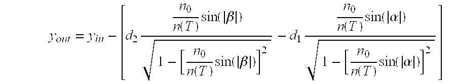
- where Y in is the position along the grating at which the light is input, n(T) is the temperature dependent index of refraction for the material used to form the pieces of the grating, n0 is the index of refraction of the material in which the grating is placed (e.g., air), and d1 and d2 are the thicknesses of the first and second pieces, respectively. When d1=d2 and |α|=|β|, the output position yout is substantially temperature independent.
- One advantage of the transmission gratings of FIGS. 4, 5, 8, 9, 10, and 12 is that the grating structure is within the substrate. This facilitates keeping foreign material out of the grating and reducing degradation of the grating due to exposure to outside elements. The internal transmission grating structures also exhibit higher grating efficiency than open transmission grating structures, as can be demonstrated by numerical solution of Maxwell's equations. In addition, it is possible to coat both outer surfaces of the transmission grating with an antireflection coating to reduce losses due to reflection.
- The transmission grating can also have one or more advantages over other wavelength dispersing components. For example, the transmission grating does not require a reflective layer (e.g., a reflective metal layer) disposed over the grated substrate as used in typical reflective gratings. This can reduce the number of manufacturing steps and can reduce the number of material-related errors that can arise, such as, for example, imperfections in the reflective layer. In addition, there can be a geometrical advantage, because the transmission gratings do not block each other and they can introduce more degrees of freedom in a device design, as opposed to most optical elements that are typically used on-axis.
- In the preceding description and Figures, the grating (whether a reflective or transmission grating) has been illustrated as an individual optical component. Alternatively, the grating can be formed on a substrate, as illustrated in FIG. 7. As an example, the
optical structure 700 illustrated in FIG. 7 includes asubstrate 702 having formed therein agrating 704 and awaveguiding layer 706 that carries light to and, optionally, from the grating. A top layer (not shown) is typically formed over the wave guiding layer. Other configurations of optical elements on a substrate can be formed. - The structural parameters of the grating structure can be selected to obtain the desired diffraction properties. These parameters include, for example, the grating period (for example, the average center-to-center distance between two teeth or wells, which can be described as the number of grating lines per mm), the grating depth, the aspect ratio (for example, the well width divided by depth of the grating), the duty cycle (for example, the tooth width divided by grating period, in FIG. 2, the duty cycle is 50%), the angle of blazing for blazed gratings, and the grating chirp (grating period variation, whether intended or not).
- In some embodiments, the parameters of the grating are selected to result in at least 50%, 75%, or 90% or more of the light being diffracted into a single diffraction order. Typically, this diffraction order is not the zero order, because zero order diffraction results in no wavelength dispersion. The diffraction of light into a single diffraction order or a small number of diffraction orders can be facilitated by a numerical optimization procedure with a piece of software (e.g., Gsolver™ available from Grating Solver Development Company, Allen, Tex.). Preferably, the grating parameters are selected so that the diffraction efficiency for the chosen order is high and substantially equal across the entire desired bandwidth of the grating. Factors that can influence the selection of grating parameters include, for example, high diffraction efficiency for a particular wavelength range, angle of incidence, and polarization; desired grating and device geometry; materials used for the grating; and manufacturability of the grating. Methods for selecting the structural parameters to obtain the desired amount of diffraction into a desired diffraction order are known in the art. Examples and optimization of transmission gratings are also known.
- In addition, in some embodiments, the structural parameters are selected so that the difference in the percentage of light being diffracted into a desired diffraction order for the TM and TE polarizations of light is no more than 10%, 5%, or even 2%. In some embodiments, the grating structure is formed to have at least 85%, 90%, 95%, or even 99% diffraction efficiency for both TM and TE polarizations. FIG. 3 illustrates a schematic graph of diffraction efficiency versus grating depth for TM and TE polarizations of light using a quartz transmission grating. As illustrated in the graph, to obtain the highest, substantially uniform diffraction efficiency for both polarizations (point A of FIG. 3) requires a substantially deep grating. Substantially uniform grating efficiency for both polarizations can also be obtained for lower levels of overall grating efficiency (point B of FIG. 3) utilizing a shallower grating. The deep grating typically results in grating structures with relatively large aspect ratios. For example, for optical communications applications, the width of a well in a square/rectangular well grating is typically about 300 to 1000 nm. The depth of the well can be in the range of 1.5 to 10 μm giving an aspect ratio (depth:well width) of 3:1, 5:1, 7:1, 10:1, 12:1, 15:1 or more to obtain high diffraction efficiency for both TM and TE polarizations.
- Another method for obtaining substantially uniform diffraction efficiency for both TE and TM polarizations, if desired, includes splitting the TE and TM polarizations into individual light beams, turning the polarization of one beam by 90 degrees, and then using a grating having the desired diffraction efficiency for only one polarization. In another method, the TE and TM polarizations are split into two beams. One beam is sent to a first grating that has high diffraction efficiency for that polarization and the second beam is directed to a second grating that has high diffraction efficiency for the other polarization. These two beams are then recombined (e.g., focused at a single position).
- The grating structure can be formed by a variety of techniques. One technique includes mechanical ruling using a stylus or other ruling device having a hard tip, such as diamond or silicon carbide. Other techniques include the use of photolithographic methods, including mask-based photolithography; lithographic methods using a holographic mask, e.g., near-field holography; and direct holographic exposure to form a grating pattern in a photoresist material deposited on the substrate. The substrate can then be etched according to the grating pattern using any wet or dry etching techniques to form the grating. Appropriate wet and dry etching techniques and etchants typically depend on the material used for the substrate.
- High aspect ratio grating structures can be formed by aligning grating structures formed in two different pieces of a substrate, as illustrated in FIG. 5. Alternatively, the high aspect ratio grating structures can be formed in a single substrate. A new method of preparing a high aspect ratio grating is schematically illustrated in FIGS. 6A to 6G. In this method, a
suitable substrate 100 is selected. The substrate can be a single material or one or more layers disposed on a base layer. Thesubstrate 100 includes the material in which the grating structure will be formed. Generally, this material is selected to be substantially transparent in the wavelength range of light that is to be diffracted using the grating structure. Preferably, the material has little absorption (e.g., no more than 5% or 10%) in that wavelength range. For many communications applications, which utilize light having wavelengths in the range of about 1200 to 1600 nm, suitable materials from which the grating structure can be formed include, for example, quartz, silica (SiOx), silicon, silicon nitride, silicon oxynitride (SiOxNy), and glass (including alkali glasses). The optional base layer can be made using any material including, for example, quartz, silica, silicon, and glass (including alkali glasses). - Typically, a
masking layer 102 is disposed on thesubstrate 100. Themasking layer 102 will be patterned, as described below, and used to protect regions of the substrate from etching in subsequent process steps. Generally, the masking layer can be formed using any material that is sufficiently resistant to the etchant used to form the grating structure so that thesubstrate 100 below the patterned masking layer is not substantially etched. Suitable materials for themasking layer 102 include, for example, metals, such as chromium, aluminum, and nickel; alloys or metal mixtures, such as nickel/chromium; silicides, such as titanium silicide; silicon nitride; silicon carbide; diamond; and silicon. The masking layer can be formed using any suitable layer formation techniques including, for example, chemical vapor deposition, physical vapor deposition such as sputtering and evaporation, sublimation, reactive conversion of a layer into another material (e.g., silicide formation), and coating. - The thickness of the
masking layer 102 can depend on factors such as, for example, the resistance of the material to the etchant used to form the grating structure, the technique used to form the masking layer, and the desired depth of the grating structure. Examples of suitable thicknesses for the masking layer are in the range of 100 nm to 1000nm. - After formation of the
masking layer 102, aphotoresist layer 104 is formed over themasking layer 102, as illustrated in FIG. 6B. Any photoresist material can be used for the photoresist layer, including any negative or positive photoresist materials. In some alternative embodiments, the photoresist material and its thickness are selected such that the photoresist layer can also be used as the masking layer 102 (i.e., the photoresist material sufficiently resists the etchant used to form the grating structure). In such embodiments, a separate masking layer is not needed. - The photoresist layer is developed by selective exposure to light to form a patterned
photoresist layer 106, as illustrated in FIG. 6C. Any photolithographic technique can be used, including, the formation of a pattern in thephotoresist layer 104 by exposure of the photoresist layer to light through a mask or by a holographic exposure created by interference between light beams split from a coherent light source. In preferred embodiments, the holographic exposure is performed without a mask and is generated by constructive and destructive interference of light from the two light beams. This can facilitate the formation of a grating pattern, including grating patterns having a period of 2 to 3 μm or less. - Following formation of the pattern in the
photoresist layer 104, the photoresist layer is etched to form a patternedphotoresist layer 106 as illustrated in FIG. 6C. Any wet or dry etching technique can be used. In some instances, wet etching techniques are less preferred for any of the etching steps described herein because residue from the wet components may be left behind or absorbed by the substrate. This residue can later contaminate the grating structure as the residue diffuses, evaporates, or otherwise leaves the substrate. - The
masking layer 102 is also etched to form apatterned masking layer 108, as illustrated in FIG. 6D. This etching can occur simultaneous to or subsequent to the etching of thephotoresist layer 104 to form the patternedphotoresist layer 106. In some instances, because the masking layer is formed of a harder or substantially different material, the photoresist layer and masking layer are separately etched. Any wet or dry etching technique can be used. One particularly suitable etching technique is reactive ion etching (RIE). The etching technique and etchant are typically selected so that thesubstrate 100 is not substantially etched. Thus, thesubstrate 100 acts as an etch stop. - In an alternative method, the masking layer is formed on a previously patterned photoresist layer. The patterned portion of the photoresist layer is then dissolved in a solvent solution. This lifts off the portion of the masking layer to expose the substrate according to the pattern.
- Returning to FIGS. 6A to 6G, after forming the patterned photoresist and masking
layers grating envelope pattern 110 is formed using a photoresist material (and, optionally, a masking material), as illustrated in FIG. 6E. Thisgrating envelope pattern 110 is typically formed using any photolithographic technique, including methods substantially similar to those discussed above for the formation of the patternedphotoresist layer 106. The grating envelope pattern surrounds the region of the substrate in which the grating structure is to be formed so that there is no stray etching in other regions. This is particularly useful when the grating pattern is formed holographically without a mask. Alternatively, the patternedphotoresist layer 106, andpatterned masking layer 108 can be formed and patterned in a manner (e.g., using a mask) that generates a grating envelope without the additional processing steps. - The
substrate 100 is then etched to form thegrating structure 112, as illustrated in FIG. 6F. Thegrating structure 112 has wells formed into thesubstrate 100 with an aspect ratio (depth:width) of at least 3:1. Typically, the well width is no more than 1 μm. The aspect ratio can be 5:1, 10:1, 12:1, 15:1 or greater. This typically requires the use of specialized etching techniques, such as, for example, deep reactive ion etching (DRIE) using, for example, high density plasma etching equipment. Examples of suitable devices for this technique include the ICP 380 Plasmalab system from Oxford Instruments, U.K. or the Omega™ 201-1-M0RI from Trikon Technologies, U.K. The etching can be performed as a timed etch to obtain a desired grating depth. Alternatively, an etch stop, such as a buried layer of silicon or another material, can be provided to indicate that the desired grating depth has been achieved. A silicon etch stop could be converted into silicon dioxide subsequently by oxidation. - After forming the
grating structure 112, the patternedmasking layer 108, the patternedphotoresist layer 106, and the optionalgrating envelope pattern 110 are removed, as illustrated in FIG. 6G. The removal of these layers can be performed using, for example, wet or dry etching techniques selective to the base material. - After formation of the
grating structure 112, the second piece of the transmission grating can be coupled to the first piece containing the grating structure, as described above. As an option, after formation of the grating structure, the grating structure can be filled with a dielectric material different from the substrate. Examples of suitable materials include silica, silicon, silicon nitride, silicon oxynitride, and plastics. Such materials can be deposited by a variety of techniques, including, for example, spin coating techniques, physical vapor deposition such as sputtering and evaporation, and PECVD, LPCVD, or other chemical vapor deposition techniques, as described above. In some instances, only a portion of the grating structure is filled, as illustrated in FIG. 9. - After filling the grating structure, the filling material, which typically extends at least several micrometers above the top surface of the substrate can be planarized to give a substantially smooth surface for coupling to the other piece of the transmission grating. This planarized surface can be above the surface of the substrate or the planarization can be performed to expose the surface of the substrate so that the filling material is substantially provided only within the grating structure. The planarization can be accomplished using, for example, chemical, mechanical, or chemical/mechanical polishing processes.
- By way of example, a grating structure can be formed in quartz with a period of 1035 nm and a duty cycle of 51%. Each grating line has a depth of 6.7 μm, a well width of about 500 nm, and a length of 1 to 10 mm. The grating structure is bonded to a second quartz piece. The calculated first order diffraction efficiency for TE polarization is 97.8% and for TM polarization is 96.6%, as calculated by Gsolver™ 4.1 for a wavelength of 1550 run and 32° angle of incidence.
- As another example, a grating structure can be formed on a quartz base material using silicon nitride (refractive index of 2.0) for the grating structure with a period of 1042 nm and a duty cycle of 51%. Each grating line has a depth of 2.0 μm, a well width of about 500 nm, and a length of 1 to 10 mm. The grating structure is bonded to a second quartz piece. The calculated first order diffraction efficiency for TE polarization is 89% and for TM polarization is 98%, as calculated by Gsolver™ 4.1 for a wavelength of 1550 nm and 32° angle of incidence.
- As an alternative to making an isolated transmission grating, a transmission grating structure can be formed in a waveguiding layer, as described above. In one example, the waveguiding layer has single mode confinement in the vertical direction (by selecting the thickness of the waveguiding layer) and no confinement in the horizontal direction. This waveguiding layer is formed on any substrate to provide structural support. A suitable waveguiding layer for optical communications, as described above, is silicon oxynitride. Other possible waveguiding materials include, for example, silicon dioxide, silicon nitride, silicon, and plastics.
- The grating structure is formed as a series of cuts through the waveguide films. In this embodiment, the horizontal length, as opposed to the depth, corresponds to the dimension illustrated as the x-axis of FIG. 3. Thus, a grating structure can be formed, as described above with a period of 1035 nm and a duty cycle of 51%. Each grating line has a horizontal depth of 6.7 μm, a well width of about 500 nm, and a vertical length of 5 μm. The grating structure is optionally filled with another material, such as a polymer, silicon oxide, or silicon nitride. Otherwise, the grating structure is filled with air or another gas.
- The present invention should not be considered limited to the particular examples described above, but rather should be understood to cover all aspects of the invention as fairly set out in the attached claims. Various modifications, equivalent processes, as well as numerous structures to which the present invention may be applicable will be readily apparent to those of skill in the art to which the present invention is directed upon review of the instant specification.
Claims (39)
Priority Applications (4)
| Application Number | Priority Date | Filing Date | Title |
|---|---|---|---|
| US09/789,888 US6762880B2 (en) | 2001-02-21 | 2001-02-21 | Grating structures and methods of making the grating structures |
| EP02741110A EP1366379A2 (en) | 2001-02-21 | 2002-02-20 | Grating structures and methods of making the grating structures |
| PCT/IB2002/002871 WO2002086560A2 (en) | 2001-02-21 | 2002-02-20 | Grating structures and methods of making the grating structures |
| AU2002314474A AU2002314474A1 (en) | 2001-02-21 | 2002-02-20 | Grating structures and methods of making the grating structures |
Applications Claiming Priority (1)
| Application Number | Priority Date | Filing Date | Title |
|---|---|---|---|
| US09/789,888 US6762880B2 (en) | 2001-02-21 | 2001-02-21 | Grating structures and methods of making the grating structures |
Publications (2)
| Publication Number | Publication Date |
|---|---|
| US20020135876A1 true US20020135876A1 (en) | 2002-09-26 |
| US6762880B2 US6762880B2 (en) | 2004-07-13 |
Family
ID=25148987
Family Applications (1)
| Application Number | Title | Priority Date | Filing Date |
|---|---|---|---|
| US09/789,888 Expired - Fee Related US6762880B2 (en) | 2001-02-21 | 2001-02-21 | Grating structures and methods of making the grating structures |
Country Status (4)
| Country | Link |
|---|---|
| US (1) | US6762880B2 (en) |
| EP (1) | EP1366379A2 (en) |
| AU (1) | AU2002314474A1 (en) |
| WO (1) | WO2002086560A2 (en) |
Cited By (28)
| Publication number | Priority date | Publication date | Assignee | Title |
|---|---|---|---|---|
| US20030090802A1 (en) * | 2001-11-12 | 2003-05-15 | Network Photonics, Inc | High-efficiency low-polarization-dependent-loss lamellar diffraction-grating profile and production process |
| FR2843203A1 (en) * | 2002-07-31 | 2004-02-06 | Jobin Yvon Sa | Surface-relief transmission diffraction grating in which the modulation height and average separation of the grating lines is selected so that S and P polarization components are transmitted with 10 percent efficiency |
| US20040033003A1 (en) * | 2002-08-16 | 2004-02-19 | Ansheng Liu | Silicon-based tunable single passband optical filter |
| WO2004029678A1 (en) * | 2001-09-14 | 2004-04-08 | Fibera, Inc | Optical grating fabrication |
| US20040136073A1 (en) * | 2002-11-01 | 2004-07-15 | Sumitomo Electric Industries, Ltd. | Transmitted type diffractive optical element |
| WO2004081620A1 (en) | 2003-03-13 | 2004-09-23 | Asahi Glass Company Limited | Diffraction element and optical device |
| US20040212890A1 (en) * | 2003-01-24 | 2004-10-28 | Manabu Shiozaki | Diffraction grating element |
| US20050007586A1 (en) * | 2003-07-09 | 2005-01-13 | Ibsen Photonics A/S | Transmission spectrometer with improved spectral and temperature characteristics |
| US6900939B2 (en) * | 2002-02-28 | 2005-05-31 | Canon Kabushiki Kaisha | Polarization insensitive beam splitting grating and apparatus using it |
| US20050196528A1 (en) * | 2004-03-05 | 2005-09-08 | Muneharu Akiyoshi | Method of manufacturing display device |
| EP1596226A1 (en) * | 2003-02-18 | 2005-11-16 | Sumitomo Electric Industries, Ltd. | Diffraction lattice element, production method for diffraction lattice element, and design method for diffraction lattice element |
| US20080038660A1 (en) * | 2004-05-21 | 2008-02-14 | Sergio Doneda | Method Of Making Grating Structures Having High Aspect Ratio |
| WO2008017458A1 (en) * | 2006-08-07 | 2008-02-14 | Fraunhofer-Gesellschaft Zur Förderung Der Amgewamdten Forschung E.V. | Enclosed, binary transmission grating |
| US20080316493A1 (en) * | 2007-06-19 | 2008-12-25 | Mitutoyo Corporation | Surface reflection encoder scale and surface reflection encoder using the same |
| US20090116790A1 (en) * | 2007-11-05 | 2009-05-07 | Mossberg Thomas W | Highly efficient optical gratings with reduced thickness requirements and impedance- matching layers |
| US20090128908A1 (en) * | 2005-11-09 | 2009-05-21 | Tatsuhiro Nakazawa | Polarization Split Element and Production Method Thereof, and Optical Pickup, Optical Device, Optical Isolator and Polarizing Hologram Provided with the Polarization Split Element |
| WO2010127339A2 (en) * | 2009-05-01 | 2010-11-04 | Toyota Motor Engineering And Manufacturing North America, Inc. | Grating structure for directing non-polarized light |
| US20120092771A1 (en) * | 2010-10-18 | 2012-04-19 | International Business Machines Corporation | Embedded vertical optical grating for heterogeneous integration |
| US20150063753A1 (en) * | 2013-09-05 | 2015-03-05 | Southern Methodist University | Enhanced coupling strength gratings |
| CN104459852A (en) * | 2013-09-22 | 2015-03-25 | 清华大学 | Preparation method of metal grating |
| WO2018039271A1 (en) * | 2016-08-22 | 2018-03-01 | Magic Leap, Inc. | Nanograting method and apparatus |
| CN108474878A (en) * | 2016-01-08 | 2018-08-31 | 大日本印刷株式会社 | Diffraction optical element and light irradiation device |
| WO2020009748A1 (en) | 2018-06-29 | 2020-01-09 | Applied Materials, Inc. | Using flowable cvd to gap fill micro/nano structures for optical components |
| US10802184B2 (en) | 2014-04-28 | 2020-10-13 | Ii-Vi Delaware Inc. | Reflective diffraction gratings employing efficiency enhancement or etch barrier layers |
| JP2021530736A (en) * | 2018-07-13 | 2021-11-11 | バリアン・セミコンダクター・エクイップメント・アソシエイツ・インコーポレイテッド | Systems and methods for optimally forming a grid of diffractive optics |
| US20220075109A1 (en) * | 2019-01-31 | 2022-03-10 | Facebook Technologies, Llc | Duty cycle range increase for waveguide combiners |
| CN114325907A (en) * | 2020-09-30 | 2022-04-12 | 京东方科技集团股份有限公司 | Wavy grating, display panel and manufacturing method of wavy grating |
| TWI827934B (en) * | 2020-06-03 | 2024-01-01 | 美商應用材料股份有限公司 | Waveguide combiner and method of fabricating the same |
Families Citing this family (17)
| Publication number | Priority date | Publication date | Assignee | Title |
|---|---|---|---|---|
| JP2003297718A (en) * | 2002-03-29 | 2003-10-17 | Seiko Epson Corp | Fine hole forming method, semiconductor device manufacturing method, semiconductor device, display, and electronic apparatus |
| US7065271B2 (en) * | 2002-10-25 | 2006-06-20 | Intel Corporation | Optical grating coupler |
| US20040201892A1 (en) * | 2003-04-03 | 2004-10-14 | Sumitomo Electric Industries, Ltd. | Diffraction grating element, optical module and optical communications system |
| JP4608679B2 (en) * | 2005-03-17 | 2011-01-12 | 財団法人新産業創造研究機構 | Manufacturing method of phase type diffraction grating and amplitude type diffraction grating used in X-ray Talbot interferometer |
| US7554734B1 (en) | 2006-04-28 | 2009-06-30 | Johan Christer Holm | Polarization independent grating |
| US20110043918A1 (en) * | 2006-12-08 | 2011-02-24 | David Thomas Crouse | Devices and methods for light control in material composites |
| KR20080075753A (en) * | 2007-02-13 | 2008-08-19 | 삼성전자주식회사 | Wire grid polarizer and method of manufacturing the same |
| US8116002B2 (en) * | 2007-08-27 | 2012-02-14 | Lumella Inc. | Grating device with adjusting layer |
| JP2011509418A (en) * | 2007-12-10 | 2011-03-24 | リサーチ・ファウンデーション・オブ・ザ・シティー・ユニヴァーシティー・オブ・ニュー・ヨーク | Subwavelength structure, apparatus and method for light control in material composites |
| US7751461B2 (en) * | 2008-08-01 | 2010-07-06 | Newport Corporation | Linewidth-narrowed excimer laser cavity |
| US8264773B2 (en) * | 2009-05-01 | 2012-09-11 | Toyota Motor Engineering And Manufacturing North America, Inc. | Grating structure for splitting light |
| US20110075260A1 (en) * | 2009-09-28 | 2011-03-31 | Hamamatsu Photonics K.K. | Grating device and method of fabricating the same |
| US8675279B2 (en) | 2009-12-15 | 2014-03-18 | Toyota Motor Engineering And Manufacturing North America, Inc. | Grating structure for dividing light |
| US10473834B2 (en) | 2016-11-21 | 2019-11-12 | Stmicroelectronics (Research & Development) Limited | Wafer level microstructures for an optical lens |
| FR3059110A1 (en) | 2016-11-21 | 2018-05-25 | Stmicroelectronics (Crolles 2) Sas | OPTICAL DIFFUSER AND METHOD FOR MANUFACTURING THE SAME |
| JP7025189B2 (en) * | 2017-12-05 | 2022-02-24 | 株式会社ミツトヨ | Scale and its manufacturing method |
| US11391957B2 (en) | 2018-10-29 | 2022-07-19 | Stmicroelectronics (Research & Development) Limited | Embedded transmissive diffractive optical elements |
Citations (2)
| Publication number | Priority date | Publication date | Assignee | Title |
|---|---|---|---|---|
| US6167112A (en) * | 1996-01-12 | 2000-12-26 | Bastian Nieman | X-ray microscope with zone plates |
| US20030076594A1 (en) * | 2001-01-16 | 2003-04-24 | Kramer Charles J. | Novel surface-relief diffraction grating |
Family Cites Families (30)
| Publication number | Priority date | Publication date | Assignee | Title |
|---|---|---|---|---|
| JPS5267343A (en) | 1975-10-27 | 1977-06-03 | Hitachi Ltd | Double spectroscope |
| US4251137A (en) | 1977-09-28 | 1981-02-17 | Rca Corporation | Tunable diffractive subtractive filter |
| US4153330A (en) | 1977-12-01 | 1979-05-08 | Bell Telephone Laboratories, Incorporated | Single-mode wavelength division optical multiplexer |
| US4279464A (en) | 1979-12-18 | 1981-07-21 | Northern Telecom Limited | Integrated optical wavelength demultiplexer |
| US4484797A (en) * | 1981-07-20 | 1984-11-27 | Rca Corporation | Diffractive subtractive color filter responsive to angle of incidence of polychromatic illuminating light |
| US4773063A (en) | 1984-11-13 | 1988-09-20 | University Of Delaware | Optical wavelength division multiplexing/demultiplexing system |
| DE3605516A1 (en) | 1985-02-21 | 1986-09-04 | Canon K.K., Tokio/Tokyo | OPTICAL FUNCTIONAL ELEMENT AND OPTICAL FUNCTIONAL DEVICE |
| FR2579044B1 (en) | 1985-03-13 | 1988-02-26 | Commissariat Energie Atomique | DEVICE FOR MULTIPLEXING MULTIPLE LIGHT SIGNALS IN INTEGRATED OPTICS |
| US4715027A (en) | 1986-05-29 | 1987-12-22 | Polaroid Corporation | Integrated optic multi/demultiplexer |
| US4736360A (en) | 1986-07-21 | 1988-04-05 | Polaroid Corporation | Bulk optic echelon multi/demultiplexer |
| FR2609180B1 (en) | 1986-12-31 | 1989-11-03 | Commissariat Energie Atomique | MULTIPLEXER-DEMULTIPLEXER USING A CONCAVE ELLIPTICAL NETWORK AND CONDUCTED IN INTEGRATED OPTICS |
| US4852079A (en) | 1987-11-23 | 1989-07-25 | Allied-Signal Inc. | Optical spectral analyzer |
| US5639300A (en) | 1987-12-07 | 1997-06-17 | Massachusetts Institute Of Technology | Epitaxy with reusable template |
| US5355237A (en) | 1993-03-17 | 1994-10-11 | The United States Of America As Represented By The Administrator Of The National Aeronautics And Space Administration | Wavelength-division multiplexed optical integrated circuit with vertical diffraction grating |
| US5526155A (en) | 1993-11-12 | 1996-06-11 | At&T Corp. | High-density optical wavelength division multiplexing |
| US5793912A (en) | 1994-06-09 | 1998-08-11 | Apa Optics, Inc. | Tunable receiver for a wavelength division multiplexing optical apparatus and method |
| JPH10507844A (en) * | 1994-09-09 | 1998-07-28 | ボード オブ スーパーバイザーズ オブ ルイジアナ ステート ユニバーシティ アンド アグリカルチュラル アンド メカニカル カレッジ | Micro structure and manufacturing method thereof |
| US5852505A (en) | 1994-12-28 | 1998-12-22 | Lucent Technologies Inc. | Dense waveguide division multiplexers implemented using a first stage fourier filter |
| NL9500004A (en) | 1995-01-02 | 1996-08-01 | Nederland Ptt | Integrated optical wavelength demultiplexer. |
| JPH0918452A (en) | 1995-06-30 | 1997-01-17 | Oki Electric Ind Co Ltd | Light wavelength converter element and light wavelength converter device |
| JPH0943440A (en) | 1995-07-28 | 1997-02-14 | Toshiba Corp | Integrated optical multiplexer/demultiplexer |
| US5808763A (en) | 1995-10-31 | 1998-09-15 | Jds Fitel Inc. | Optical demultiplexor |
| CA2231642A1 (en) | 1996-08-29 | 1998-03-05 | Corning Incorporated | Switchable wavelength add/drop component |
| US5745616A (en) | 1996-11-27 | 1998-04-28 | Lucent Technologies Inc. | Waveguide grating router and method of making same having relatively small dimensions |
| US6084695A (en) | 1997-02-14 | 2000-07-04 | Photonetics | Optical fiber wavelength multiplexer and demutiplexer |
| US5796479A (en) | 1997-03-27 | 1998-08-18 | Hewlett-Packard Company | Signal monitoring apparatus for wavelength division multiplexed optical telecommunication networks |
| JP3472092B2 (en) | 1997-07-28 | 2003-12-02 | キヤノン株式会社 | Diffractive optical element and optical system using the same |
| US5999672A (en) | 1997-12-13 | 1999-12-07 | Light Chip, Inc. | Integrated bi-directional dual axial gradient refractive index/diffraction grating wavelength division multiplexer |
| JP4336412B2 (en) | 1998-06-16 | 2009-09-30 | キヤノン株式会社 | Diffractive optical element and optical system using the same |
| DE60016170D1 (en) | 1999-01-08 | 2004-12-30 | Ibsen Photonics As Farum | SPECTROMETER |
-
2001
- 2001-02-21 US US09/789,888 patent/US6762880B2/en not_active Expired - Fee Related
-
2002
- 2002-02-20 WO PCT/IB2002/002871 patent/WO2002086560A2/en not_active Application Discontinuation
- 2002-02-20 EP EP02741110A patent/EP1366379A2/en not_active Withdrawn
- 2002-02-20 AU AU2002314474A patent/AU2002314474A1/en not_active Abandoned
Patent Citations (2)
| Publication number | Priority date | Publication date | Assignee | Title |
|---|---|---|---|---|
| US6167112A (en) * | 1996-01-12 | 2000-12-26 | Bastian Nieman | X-ray microscope with zone plates |
| US20030076594A1 (en) * | 2001-01-16 | 2003-04-24 | Kramer Charles J. | Novel surface-relief diffraction grating |
Cited By (69)
| Publication number | Priority date | Publication date | Assignee | Title |
|---|---|---|---|---|
| WO2004029678A1 (en) * | 2001-09-14 | 2004-04-08 | Fibera, Inc | Optical grating fabrication |
| US20030090802A1 (en) * | 2001-11-12 | 2003-05-15 | Network Photonics, Inc | High-efficiency low-polarization-dependent-loss lamellar diffraction-grating profile and production process |
| US6900939B2 (en) * | 2002-02-28 | 2005-05-31 | Canon Kabushiki Kaisha | Polarization insensitive beam splitting grating and apparatus using it |
| FR2843203A1 (en) * | 2002-07-31 | 2004-02-06 | Jobin Yvon Sa | Surface-relief transmission diffraction grating in which the modulation height and average separation of the grating lines is selected so that S and P polarization components are transmitted with 10 percent efficiency |
| US20040033003A1 (en) * | 2002-08-16 | 2004-02-19 | Ansheng Liu | Silicon-based tunable single passband optical filter |
| US7245792B2 (en) * | 2002-08-16 | 2007-07-17 | Intel Corporation | Silicon-based tunable single passband optical filter |
| US20040136073A1 (en) * | 2002-11-01 | 2004-07-15 | Sumitomo Electric Industries, Ltd. | Transmitted type diffractive optical element |
| US7085054B2 (en) | 2003-01-24 | 2006-08-01 | Sumitomo Electric Industries, Ltd. | Diffraction grating element |
| US20040212890A1 (en) * | 2003-01-24 | 2004-10-28 | Manabu Shiozaki | Diffraction grating element |
| US6917471B2 (en) | 2003-01-24 | 2005-07-12 | Sumitomo Electric Industries, Ltd. | Diffraction grating element |
| US20060262305A1 (en) * | 2003-01-24 | 2006-11-23 | Sumitomo Electric Industries, Ltd. | Diffraction grating element |
| US20050231805A1 (en) * | 2003-01-24 | 2005-10-20 | Sumitomo Electric Industries, Ltd. | Diffraction grating element |
| JP4600577B2 (en) * | 2003-02-18 | 2010-12-15 | 住友電気工業株式会社 | Diffraction grating element |
| EP2214037A1 (en) * | 2003-02-18 | 2010-08-04 | Sumitomo Electric Industries, Ltd. | Diffraction grating element, and production method of diffraction grating element |
| JPWO2004074888A1 (en) * | 2003-02-18 | 2006-06-01 | 住友電気工業株式会社 | Diffraction grating element, diffraction grating element manufacturing method, and diffraction grating element design method |
| EP1596226A1 (en) * | 2003-02-18 | 2005-11-16 | Sumitomo Electric Industries, Ltd. | Diffraction lattice element, production method for diffraction lattice element, and design method for diffraction lattice element |
| JP4600578B2 (en) * | 2003-02-18 | 2010-12-15 | 住友電気工業株式会社 | Diffraction grating element |
| EP1596226A4 (en) * | 2003-02-18 | 2009-09-02 | Sumitomo Electric Industries | Diffraction lattice element, production method for diffraction lattice element, and design method for diffraction lattice element |
| JP4600579B2 (en) * | 2003-02-18 | 2010-12-15 | 住友電気工業株式会社 | Diffraction grating element |
| JP2009187016A (en) * | 2003-02-18 | 2009-08-20 | Sumitomo Electric Ind Ltd | Diffraction grating element |
| JP2009187017A (en) * | 2003-02-18 | 2009-08-20 | Sumitomo Electric Ind Ltd | Diffraction grating element |
| JP2009187018A (en) * | 2003-02-18 | 2009-08-20 | Sumitomo Electric Ind Ltd | Diffraction grating element |
| EP1602947A4 (en) * | 2003-03-13 | 2007-03-28 | Asahi Glass Co Ltd | Diffraction element and optical device |
| EP1602947A1 (en) * | 2003-03-13 | 2005-12-07 | Asahi Glass Company Ltd. | Diffraction element and optical device |
| WO2004081620A1 (en) | 2003-03-13 | 2004-09-23 | Asahi Glass Company Limited | Diffraction element and optical device |
| US7180590B2 (en) * | 2003-07-09 | 2007-02-20 | Ibsen Photonics A/S | Transmission spectrometer with improved spectral and temperature characteristics |
| US20050007586A1 (en) * | 2003-07-09 | 2005-01-13 | Ibsen Photonics A/S | Transmission spectrometer with improved spectral and temperature characteristics |
| US7449215B2 (en) * | 2004-03-05 | 2008-11-11 | Toshiba Matsushita Display Technology Co., Ltd. | Method of manufacturing display device |
| US20050196528A1 (en) * | 2004-03-05 | 2005-09-08 | Muneharu Akiyoshi | Method of manufacturing display device |
| US20080038660A1 (en) * | 2004-05-21 | 2008-02-14 | Sergio Doneda | Method Of Making Grating Structures Having High Aspect Ratio |
| US20090128908A1 (en) * | 2005-11-09 | 2009-05-21 | Tatsuhiro Nakazawa | Polarization Split Element and Production Method Thereof, and Optical Pickup, Optical Device, Optical Isolator and Polarizing Hologram Provided with the Polarization Split Element |
| WO2008017458A1 (en) * | 2006-08-07 | 2008-02-14 | Fraunhofer-Gesellschaft Zur Förderung Der Amgewamdten Forschung E.V. | Enclosed, binary transmission grating |
| US7916305B2 (en) * | 2007-06-19 | 2011-03-29 | Mitutoyo Corporation | Surface reflection encoder scale and surface reflection encoder using the same |
| US20080316493A1 (en) * | 2007-06-19 | 2008-12-25 | Mitutoyo Corporation | Surface reflection encoder scale and surface reflection encoder using the same |
| US20090116790A1 (en) * | 2007-11-05 | 2009-05-07 | Mossberg Thomas W | Highly efficient optical gratings with reduced thickness requirements and impedance- matching layers |
| US8165436B2 (en) * | 2007-11-05 | 2012-04-24 | Lightsmyth Technologies Inc. | Highly efficient optical gratings with reduced thickness requirements and impedance-matching layers |
| US8989537B2 (en) | 2007-11-05 | 2015-03-24 | Lightsmyth Technologies, Inc. | Highly efficient optical gratings with reduced thickness requirements and impedance-matching layers |
| WO2010127339A3 (en) * | 2009-05-01 | 2011-02-03 | Toyota Motor Engineering And Manufacturing North America, Inc. | Grating structure for directing non-polarized light |
| US8098430B2 (en) | 2009-05-01 | 2012-01-17 | Toyota Motor Engineering And Manufacturing North America, Inc. | Grating structure for directing non-polarized light |
| US20100277937A1 (en) * | 2009-05-01 | 2010-11-04 | Toyota Motor Engineering And Manufacturing North America, Inc. | Grating structure for directing non-polarized light |
| WO2010127339A2 (en) * | 2009-05-01 | 2010-11-04 | Toyota Motor Engineering And Manufacturing North America, Inc. | Grating structure for directing non-polarized light |
| US8767299B2 (en) * | 2010-10-18 | 2014-07-01 | International Business Machines Corporation | Embedded vertical optical grating for heterogeneous integration |
| US20120092771A1 (en) * | 2010-10-18 | 2012-04-19 | International Business Machines Corporation | Embedded vertical optical grating for heterogeneous integration |
| US20150063753A1 (en) * | 2013-09-05 | 2015-03-05 | Southern Methodist University | Enhanced coupling strength gratings |
| US10620379B2 (en) | 2013-09-05 | 2020-04-14 | Southern Methodist University | Enhanced coupling strength grating having a cover layer |
| US10620378B2 (en) | 2013-09-05 | 2020-04-14 | Southern Methodist University | Method of making an enhanced coupling strength grating having a cover layer |
| US10371898B2 (en) * | 2013-09-05 | 2019-08-06 | Southern Methodist University | Enhanced coupling strength grating having a cover layer |
| CN104459852A (en) * | 2013-09-22 | 2015-03-25 | 清华大学 | Preparation method of metal grating |
| US10802184B2 (en) | 2014-04-28 | 2020-10-13 | Ii-Vi Delaware Inc. | Reflective diffraction gratings employing efficiency enhancement or etch barrier layers |
| CN108474878A (en) * | 2016-01-08 | 2018-08-31 | 大日本印刷株式会社 | Diffraction optical element and light irradiation device |
| US10983263B2 (en) | 2016-08-22 | 2021-04-20 | Magic Leap, Inc. | Diffractive waveguide and eyepiece having image multiplying grating overlapping with outcoupling grating |
| US10444419B2 (en) | 2016-08-22 | 2019-10-15 | Magic Leap, Inc. | Dithering methods and apparatus for wearable display device |
| US11604310B2 (en) | 2016-08-22 | 2023-03-14 | Magic Leap, Inc. | Multi-layer diffractive eyepiece with front cover plate and wavelength-selective reflector |
| US10481317B2 (en) | 2016-08-22 | 2019-11-19 | Magic Leap, Inc. | Nanograting method and apparatus |
| US10627559B2 (en) | 2016-08-22 | 2020-04-21 | Magic Leap, Inc. | Projector architecture incorporating artifact mitigation |
| US10725223B2 (en) | 2016-08-22 | 2020-07-28 | Magic Leap, Inc. | Multi-layer diffractive eyepiece with wavelength-selective reflector |
| WO2018039271A1 (en) * | 2016-08-22 | 2018-03-01 | Magic Leap, Inc. | Nanograting method and apparatus |
| US10823894B2 (en) | 2016-08-22 | 2020-11-03 | Magic Leaps, Inc. | Nanograting method and apparatus |
| CN109863446A (en) * | 2016-08-22 | 2019-06-07 | 奇跃公司 | Nanometer method and apparatus |
| US11428859B2 (en) | 2016-08-22 | 2022-08-30 | Magic Leap, Inc. | Projector architecture incorporating artifact mitigation |
| US11822112B2 (en) | 2016-08-22 | 2023-11-21 | Magic Leap, Inc. | Projector architecture incorporating artifact mitigation |
| EP3814811A4 (en) * | 2018-06-29 | 2022-03-16 | Applied Materials, Inc. | Using flowable cvd to gap fill micro/nano structures for optical components |
| WO2020009748A1 (en) | 2018-06-29 | 2020-01-09 | Applied Materials, Inc. | Using flowable cvd to gap fill micro/nano structures for optical components |
| CN112384831A (en) * | 2018-06-29 | 2021-02-19 | 应用材料公司 | Gap filling of micro/nano structures for optical components using flowable CVD |
| JP2021530736A (en) * | 2018-07-13 | 2021-11-11 | バリアン・セミコンダクター・エクイップメント・アソシエイツ・インコーポレイテッド | Systems and methods for optimally forming a grid of diffractive optics |
| JP7288950B2 (en) | 2018-07-13 | 2023-06-08 | バリアン・セミコンダクター・エクイップメント・アソシエイツ・インコーポレイテッド | Systems and methods for optimally forming gratings in diffractive optical elements |
| US20220075109A1 (en) * | 2019-01-31 | 2022-03-10 | Facebook Technologies, Llc | Duty cycle range increase for waveguide combiners |
| TWI827934B (en) * | 2020-06-03 | 2024-01-01 | 美商應用材料股份有限公司 | Waveguide combiner and method of fabricating the same |
| CN114325907A (en) * | 2020-09-30 | 2022-04-12 | 京东方科技集团股份有限公司 | Wavy grating, display panel and manufacturing method of wavy grating |
Also Published As
| Publication number | Publication date |
|---|---|
| AU2002314474A1 (en) | 2002-11-05 |
| WO2002086560A3 (en) | 2003-06-05 |
| US6762880B2 (en) | 2004-07-13 |
| WO2002086560A2 (en) | 2002-10-31 |
| EP1366379A2 (en) | 2003-12-03 |
Similar Documents
| Publication | Publication Date | Title |
|---|---|---|
| US6762880B2 (en) | Grating structures and methods of making the grating structures | |
| US7393793B2 (en) | Tunable-wavelength optical filter and method of manufacturing the same | |
| JP3902678B2 (en) | Manufacturing method of diffraction grating and light guide | |
| US20150029588A1 (en) | Control of Light Wavefronts | |
| KR20050105383A (en) | Wire grid polarizer and thereof manufacture method | |
| US9157799B2 (en) | Optical wavelength dispersion device and method of manufacturing the same | |
| JP2007538275A (en) | Method for manufacturing a diffraction grating structure having a high aspect ratio | |
| US9910195B2 (en) | Optical wavelength dispersion device and method of manufacturing the same | |
| US8279525B2 (en) | Three-dimensional diffractive structure, method for making, and applications thereof | |
| US8092701B2 (en) | Grating, negative and replica gratings of the grating, and method of manufacturing the same | |
| JP2002169022A (en) | Optical element, spectroscopic device and integrated optical device using the same | |
| JP3675314B2 (en) | Diffraction grating | |
| US6428944B1 (en) | Fabrication of gratings in planar waveguide devices | |
| US6756185B2 (en) | Method for making integrated optical waveguides and micromachined features | |
| JPH06317705A (en) | Diffraction element and optical multiplxing/ demultiplxing device using the same | |
| JP4151073B2 (en) | Optical element and manufacturing method thereof | |
| JP4162976B2 (en) | Optical element using one-dimensional photonic crystal | |
| Roth | SPACE VARIANT GUIDED MODE RESONANCE FILTERS | |
| JPH11305023A (en) | Production of silicon diffraction grating | |
| Huang | Design and fabrication of polymeric waveguide Bragg grating devices | |
| Lee et al. | Si-based UV transparent subwavelength optical elements | |
| Ho | Grating based multi/demultiplexing devices for wavelength division multiplexing network systems |
Legal Events
| Date | Code | Title | Description |
|---|---|---|---|
| AS | Assignment |
Owner name: ADC DANMARK APS, DENMARK Free format text: ASSIGNMENT OF ASSIGNORS INTEREST;ASSIGNORS:HOLM JOHAN CHRISTER;MADSEN, HENRIK;WEICHEL, STEEN;AND OTHERS;REEL/FRAME:011835/0055;SIGNING DATES FROM 20010221 TO 20010305 |
|
| AS | Assignment |
Owner name: IBSEN PHOTONICS A/S, DENMARK Free format text: ASSIGNMENT OF ASSIGNORS INTEREST;ASSIGNOR:ADC DANMARK APS;REEL/FRAME:012804/0933 Effective date: 20011031 |
|
| FPAY | Fee payment |
Year of fee payment: 4 |
|
| REMI | Maintenance fee reminder mailed | ||
| LAPS | Lapse for failure to pay maintenance fees | ||
| STCH | Information on status: patent discontinuation |
Free format text: PATENT EXPIRED DUE TO NONPAYMENT OF MAINTENANCE FEES UNDER 37 CFR 1.362 |
|
| FP | Lapsed due to failure to pay maintenance fee |
Effective date: 20120713 |