US12347380B2 - Display apparatus - Google Patents
Display apparatus Download PDFInfo
- Publication number
- US12347380B2 US12347380B2 US18/600,515 US202418600515A US12347380B2 US 12347380 B2 US12347380 B2 US 12347380B2 US 202418600515 A US202418600515 A US 202418600515A US 12347380 B2 US12347380 B2 US 12347380B2
- Authority
- US
- United States
- Prior art keywords
- display area
- insulating layer
- display
- groove
- contact portion
- Prior art date
- Legal status (The legal status is an assumption and is not a legal conclusion. Google has not performed a legal analysis and makes no representation as to the accuracy of the status listed.)
- Active
Links
Images


Classifications
-
- G—PHYSICS
- G09—EDUCATION; CRYPTOGRAPHY; DISPLAY; ADVERTISING; SEALS
- G09G—ARRANGEMENTS OR CIRCUITS FOR CONTROL OF INDICATING DEVICES USING STATIC MEANS TO PRESENT VARIABLE INFORMATION
- G09G3/00—Control arrangements or circuits, of interest only in connection with visual indicators other than cathode-ray tubes
- G09G3/20—Control arrangements or circuits, of interest only in connection with visual indicators other than cathode-ray tubes for presentation of an assembly of a number of characters, e.g. a page, by composing the assembly by combination of individual elements arranged in a matrix no fixed position being assigned to or needed to be assigned to the individual characters or partial characters
- G09G3/22—Control arrangements or circuits, of interest only in connection with visual indicators other than cathode-ray tubes for presentation of an assembly of a number of characters, e.g. a page, by composing the assembly by combination of individual elements arranged in a matrix no fixed position being assigned to or needed to be assigned to the individual characters or partial characters using controlled light sources
- G09G3/30—Control arrangements or circuits, of interest only in connection with visual indicators other than cathode-ray tubes for presentation of an assembly of a number of characters, e.g. a page, by composing the assembly by combination of individual elements arranged in a matrix no fixed position being assigned to or needed to be assigned to the individual characters or partial characters using controlled light sources using electroluminescent panels
- G09G3/32—Control arrangements or circuits, of interest only in connection with visual indicators other than cathode-ray tubes for presentation of an assembly of a number of characters, e.g. a page, by composing the assembly by combination of individual elements arranged in a matrix no fixed position being assigned to or needed to be assigned to the individual characters or partial characters using controlled light sources using electroluminescent panels semiconductive, e.g. using light-emitting diodes [LED]
- G09G3/3208—Control arrangements or circuits, of interest only in connection with visual indicators other than cathode-ray tubes for presentation of an assembly of a number of characters, e.g. a page, by composing the assembly by combination of individual elements arranged in a matrix no fixed position being assigned to or needed to be assigned to the individual characters or partial characters using controlled light sources using electroluminescent panels semiconductive, e.g. using light-emitting diodes [LED] organic, e.g. using organic light-emitting diodes [OLED]
- G09G3/3225—Control arrangements or circuits, of interest only in connection with visual indicators other than cathode-ray tubes for presentation of an assembly of a number of characters, e.g. a page, by composing the assembly by combination of individual elements arranged in a matrix no fixed position being assigned to or needed to be assigned to the individual characters or partial characters using controlled light sources using electroluminescent panels semiconductive, e.g. using light-emitting diodes [LED] organic, e.g. using organic light-emitting diodes [OLED] using an active matrix
- G09G3/3233—Control arrangements or circuits, of interest only in connection with visual indicators other than cathode-ray tubes for presentation of an assembly of a number of characters, e.g. a page, by composing the assembly by combination of individual elements arranged in a matrix no fixed position being assigned to or needed to be assigned to the individual characters or partial characters using controlled light sources using electroluminescent panels semiconductive, e.g. using light-emitting diodes [LED] organic, e.g. using organic light-emitting diodes [OLED] using an active matrix with pixel circuitry controlling the current through the light-emitting element
-
- H—ELECTRICITY
- H10—SEMICONDUCTOR DEVICES; ELECTRIC SOLID-STATE DEVICES NOT OTHERWISE PROVIDED FOR
- H10K—ORGANIC ELECTRIC SOLID-STATE DEVICES
- H10K59/00—Integrated devices, or assemblies of multiple devices, comprising at least one organic light-emitting element covered by group H10K50/00
- H10K59/10—OLED displays
- H10K59/12—Active-matrix OLED [AMOLED] displays
- H10K59/124—Insulating layers formed between TFT elements and OLED elements
-
- H—ELECTRICITY
- H10—SEMICONDUCTOR DEVICES; ELECTRIC SOLID-STATE DEVICES NOT OTHERWISE PROVIDED FOR
- H10K—ORGANIC ELECTRIC SOLID-STATE DEVICES
- H10K59/00—Integrated devices, or assemblies of multiple devices, comprising at least one organic light-emitting element covered by group H10K50/00
- H10K59/10—OLED displays
- H10K59/12—Active-matrix OLED [AMOLED] displays
- H10K59/131—Interconnections, e.g. wiring lines or terminals
-
- G—PHYSICS
- G09—EDUCATION; CRYPTOGRAPHY; DISPLAY; ADVERTISING; SEALS
- G09G—ARRANGEMENTS OR CIRCUITS FOR CONTROL OF INDICATING DEVICES USING STATIC MEANS TO PRESENT VARIABLE INFORMATION
- G09G2300/00—Aspects of the constitution of display devices
- G09G2300/04—Structural and physical details of display devices
- G09G2300/0404—Matrix technologies
- G09G2300/0408—Integration of the drivers onto the display substrate
-
- G—PHYSICS
- G09—EDUCATION; CRYPTOGRAPHY; DISPLAY; ADVERTISING; SEALS
- G09G—ARRANGEMENTS OR CIRCUITS FOR CONTROL OF INDICATING DEVICES USING STATIC MEANS TO PRESENT VARIABLE INFORMATION
- G09G2300/00—Aspects of the constitution of display devices
- G09G2300/04—Structural and physical details of display devices
- G09G2300/0421—Structural details of the set of electrodes
- G09G2300/0426—Layout of electrodes and connections
-
- G—PHYSICS
- G09—EDUCATION; CRYPTOGRAPHY; DISPLAY; ADVERTISING; SEALS
- G09G—ARRANGEMENTS OR CIRCUITS FOR CONTROL OF INDICATING DEVICES USING STATIC MEANS TO PRESENT VARIABLE INFORMATION
- G09G2300/00—Aspects of the constitution of display devices
- G09G2300/08—Active matrix structure, i.e. with use of active elements, inclusive of non-linear two terminal elements, in the pixels together with light emitting or modulating elements
- G09G2300/0809—Several active elements per pixel in active matrix panels
- G09G2300/0819—Several active elements per pixel in active matrix panels used for counteracting undesired variations, e.g. feedback or autozeroing
-
- G—PHYSICS
- G09—EDUCATION; CRYPTOGRAPHY; DISPLAY; ADVERTISING; SEALS
- G09G—ARRANGEMENTS OR CIRCUITS FOR CONTROL OF INDICATING DEVICES USING STATIC MEANS TO PRESENT VARIABLE INFORMATION
- G09G2300/00—Aspects of the constitution of display devices
- G09G2300/08—Active matrix structure, i.e. with use of active elements, inclusive of non-linear two terminal elements, in the pixels together with light emitting or modulating elements
- G09G2300/0809—Several active elements per pixel in active matrix panels
- G09G2300/0842—Several active elements per pixel in active matrix panels forming a memory circuit, e.g. a dynamic memory with one capacitor
- G09G2300/0861—Several active elements per pixel in active matrix panels forming a memory circuit, e.g. a dynamic memory with one capacitor with additional control of the display period without amending the charge stored in a pixel memory, e.g. by means of additional select electrodes
Definitions
- aspects of one or more embodiments relate to a display apparatus.
- aspects of one or more embodiments include a high-resolution display apparatus that may be relatively robust, resistant, and flexible to external impact.
- a display apparatus includes a substrate in which a first display area, a second display area, a third display area between the first display area and the second display area, and a non-display area are defined, a first connection pixel circuit arranged in the first display area, a second connection pixel circuit arranged in the second display area, a driver circuit arranged in the third display area, a signal connection line connected to a first contact portion of the first connection pixel circuit and a second contact portion of the second connection pixel circuit and extending in a first direction to pass the third display area, and an inorganic insulating layer including a first groove between the driver circuit and at least any one of the first contact portion and the second contact portion, the first groove extending in a second direction and crossing the signal connection line in a plane.
- the first contact portion may be arranged on an edge portion of the first connection pixel circuit that is adjacent to the driver circuit, and the second contact portion may be arranged on an edge portion of the second connection pixel circuit that is adjacent to the driver circuit.
- the signal connection line may be provided in plural, and the plurality of grooves may further include a third groove between two adjacent signal connection lines among the plurality of signal connection lines.
- the first display area, the third display area, and the second display area may be arranged in the first direction.
- FIG. 2 is an example cross-sectional view of a portion of the display apparatus of FIG. 1 , taken along a line I-I′ according to some embodiments;
- FIGS. 5 and 6 are enlarged plan views showing a region II of FIG. 1 according to some embodiments.
- FIG. 7 is an example cross-sectional view of a portion of the display apparatus of FIG. 6 , taken along a line III-III′ according to some embodiments;
- FIG. 8 is an example cross-sectional view of a portion of the display apparatus of FIG. 5 , taken along a line IV-IV′ according to some embodiments.
- FIG. 9 is an example cross-sectional view of a portion of the display apparatus of FIG. 5 , taken along a line V-V′ according to some embodiments.
- the expression “at least one of a, b, or c” indicates only a, only b, only c, both a and b, both a and c, both b and c, all of a, b, and c, or any combination of a, b, and/or c.
- a layer, region, or component when a layer, region, or component is referred to as being connected to another layer, region, or component, it can be directly and/or indirectly connected to the other layer, region, or component. That is, for example, intervening layers, regions, or components may be present.
- a layer, region, or component when referred to as being electrically connected to another layer, region, or component, it can be directly or indirectly electrically connected to the other layer, region, or component.
- the x-axis, the y-axis, and the z-axis are not limited to three axes of the rectangular coordinate system, and may be interpreted in a broader sense.
- the x-axis, the y-axis, and the z-axis may be perpendicular to one another, or may represent different directions that are not perpendicular to one another.
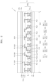
- FIG. 1 is a schematic plan view of a display apparatus according to some embodiments.
- a display apparatus 1 may display a moving image (e.g., video images) or a still image (e.g., static images) and may be used as a display screen for various products, for example, a portable electronic apparatus, such as a mobile phone, a smartphone, a tablet Personal Computer (PC), a mobile communication terminal, a personal digital assistant, an e-book terminal, a Portable Multimedia Player (PMP), a navigation device, or an Ultra Mobile PC (UMPC), a television (TV), a laptop, a monitor, a billboard, an Internet of Things (IoT) device, and the like.
- a portable electronic apparatus such as a mobile phone, a smartphone, a tablet Personal Computer (PC), a mobile communication terminal, a personal digital assistant, an e-book terminal, a Portable Multimedia Player (PMP), a navigation device, or an Ultra Mobile PC (UMPC), a television (TV), a laptop, a monitor, a billboard, an Internet of Things (IoT) device, and the like.
- the display apparatus 1 may be used in a wearable device, such as a smartwatch, a watch phone, an eyewear display, or a head-mounted display (HMD). Also, the display apparatus 1 may be used as a display screen in an instrument cluster of a vehicle, a Center Information Display (CID) mounted on a center fascia or a dashboard of a vehicle, a room mirror display replacing a side-view mirror of a vehicle, or a car headrest monitor provided for rear-seat entertainment.
- a wearable device such as a smartwatch, a watch phone, an eyewear display, or a head-mounted display (HMD).
- the display apparatus 1 may be used as a display screen in an instrument cluster of a vehicle, a Center Information Display (CID) mounted on a center fascia or a dashboard of a vehicle, a room mirror display replacing a side-view mirror of a vehicle, or a car headrest monitor provided for rear-seat entertainment.
- CID Center Information Display
- the display apparatus 1 may be overall planar, bent, or curved. According to some embodiments, the display apparatus 1 may be bent so that display surfaces may face each other. According to some embodiments, the display apparatus 1 may be bent to make the display surface face outwards.
- the term “display surface” may indicate a surface on which images are displayed, the display surface may include a display area DA and a non-display area NDA, and images may be provided to a user through the display area DA.
- the term “bent” may indicate that a shape is not constant and may be changed from an original shape to another one, and may indicate that a display surface is folded along one or more lines, that is, a folding axis, curved, or rolled like a scroll.
- the display apparatus 1 may externally provide or display images by using light emitted from the display area DA. Because the display apparatus 1 includes a substrate 100 , the substrate 100 may include the display area DA and the non-display area NDA. In other words, the display area DA and the non-display area NDA may be defined on the substrate 100 .
- the non-display area NDA may surround at least a portion of the display area DA. According to some embodiments, the non-display area NDA may surround (e.g., in a periphery or outside a footprint of) the display area DA.
- the substrate 100 may include various materials, such as glass, metals, and plastic. According to some embodiments, the substrate 100 may include a flexible material.
- the flexible material may be a material that is relatively easily curved, bent, folded, or rolled.
- the substrate 100 including the flexible material may include ultra-thin glass, metal, or plastic.
- the display area DA may have a rectangular shape.
- the display area DA may have a polygonal shape, such as a triangle, a pentagon, or a hexagon, a circular shape, an oval shape, or an atypical shape.
- the display area DA may have rounded corners, rounded edges, a general circular shape, and/or a general elliptical shape.
- pixels P including various display elements, such as organic light-emitting diodes OLED, may be arranged.
- the pixel P may be provided in the plural, and the pixels P may be arranged in various forms, such as a stripe form, a Pentile form, and a mosaic form, to realize images.
- each pixel P indicates a sub-pixel emitting light of a different color and may be, for example, one of a red sub-pixel, a green sub-pixel, and a blue sub-pixel.
- the display area DA may include any suitable number of pixels P (e.g., arranged in a matrix configuration of rows and columns) according to the design and size of the display apparatus 1 .
- an organic light-emitting display apparatus is described, but the display apparatus is not limited thereto.
- the display apparatus may be, for example, an inorganic light-emitting display apparatus (or an inorganic EL display apparatus) or a quantum dot light-emitting display apparatus.
- an emission layer of a display element included in a display apparatus may include an organic material, an inorganic material, quantum dots, both an organic material and quantum dots, both an inorganic material and quantum dots, or an organic material, an inorganic material, and quantum dots.
- the display apparatus 1 may include a display panel 10 .
- the display apparatus 1 may further include a support layer that may overlap the display panel 10 , and a cover window for protecting the display panel 10 may be further located above the display panel 10 .
- the driver circuits DC may be arranged in the third display area DA 3 . That is, the third display elements DE 3 arranged in the third display area DA 3 may overlap at least any one of the driver circuits DC.
- the driver circuits DC such as the first driver circuit DC 1 and the second driver circuit DC 2 may be arranged in the display area DA, and some of the display elements DE are located above the driver circuits DC. That is, the third display area DA 3 may include the driver circuits DC and the third display element DE 3 overlapping the same.
- the third pixel circuit PC 3 controlling the emission of the third display element DE 3 may be located in the first display area DA 1 as the third connection line CL 3 extends. Accordingly, as the driver circuitry, the power supply line, or the like may be located under the display elements DE, a dead space that may be generated because of the driver circuitry or the power supply line may be effectively relatively reduced.
- FIGS. 3 and 4 each are a schematic equivalent circuit diagram of any one of pixel circuits arranged in a display panel.
- the pixel circuits PC of pixels P shown in FIGS. 3 and 4 may be the first pixel circuit PC 1 of the first pixel P 1 , the second pixel circuit PC 2 of the second pixel P 2 , and the third pixel circuit PC 3 of the third pixel P 3 .
- the pixel circuit PC of the pixel P is referred to as a pixel circuit PC for convenience.
- FIG. 3 shows that the first transistor T 1 to the seventh transistor T 7 each are a P-type transistor.
- the first transistor T 1 to the seventh transistor T 7 may each be an N-type transistor, or some of the first transistor T 1 to the seventh transistor T 7 may each be an N-type transistor, and the others thereof may each be a P-type transistor.
- FIG. 4 shows that the third transistor T 3 and the fourth transistor T 4 among the first transistor T 1 to the seventh transistor T 7 each are an N-type transistor, and the others thereof each are a P-type transistor.
- the third transistor T 3 and the fourth transistor T 4 may respectively include semiconductor layers including oxide, and the other transistors may respectively include semiconductor layers including silicon.
- FIGS. 5 and 6 are enlarged plan views of examples of a portion of the display panel corresponding to the region II of FIG. 1 .
- the fourth groove GV 4 may extend in the first direction (e.g., the x direction) and may be arranged in the third display area DA 3 .
- the fourth groove GV 4 may be arranged between the signal connection line SCL and the driver circuit DC.
- the fourth groove GV 4 may be arranged in parallel with adjacent signal connection lines SCL.
- the grooves GV may be arranged to surround to the pixel circuit area PCA in addition to the first groove GV 1 to the fourth groove GV 4 .
- the grooves GV may be formed in a first insulating layer IL 1 described below.
- the grooves GV may have shapes in which portions of the first insulating layer IL are removed.
- the first insulating layer IL 1 may be an inorganic insulating layer and include insulating layers.
- the second insulating layer IL 2 may be buried in the grooves GV.
- the second insulating layer IL 2 may be an organic insulating layer. Because the second insulating layer IL 2 buried in the grooves GV includes an organic material, the propagation of cracks, which are formed in the first insulating layer IL 1 of a pixel because of external impact, to adjacent pixels may be prevented or relatively reduced.
- the driver circuit DC is arranged in the display area DA, and thus, the dead space may be relatively reduced and the display apparatus may be robust to the external impact. Also, in an area where the driver circuit DC is arranged, coupling occurring between adjacent signal connection lines SCL or between the signal connection line SCL and the driver circuit DC may be relatively reduced.
- the display element DE may be located above the pixel circuit PC and the driver circuit DC.
- the display element DE may be located directly on the pixel circuit PC to overlap the same or may be offset from the pixel circuit PC and arranged to partially overlap a pixel circuit PC of another pixel in an adjacent row and/or column. Alternatively, the display element DE may not overlap the pixel circuit PC connected thereto.
- the display element DE may be an organic light-emitting diode OLED.
- the first display element DE 1 and the second display element DE 2 may be arranged in the first display area DA 1 and the second display area DA 2 .
- the third display element DE 3 may be arranged in the third display area DA 3 .
- the third pixel circuit PC 3 connected to the third display element DE 3 may be arranged in the first display area DA 1 and the second display area DA 2 not in the third display area DA 3 . That is, the third display element DE 3 may be connected to the pixel circuit PC arranged in the display area DA other than the third display area DA 3 , but may be arranged above the driver circuit DC in the third display area DA 3 .
- FIG. 7 is an example cross-sectional view of a portion of the display apparatus of FIG. 6 , taken along a line III-III′.
- the display panel 10 may include the second display area DA 2 and the third display area DA 3 .
- the first pixel circuit PC 1 , the second pixel circuit PC 2 , and the third pixel circuit PC 3 may be arranged in the second display area DA 2 .
- the first driver circuit DC 1 and the second driver circuit DC 2 may be arranged.
- the first display element DE 1 electrically connected to the first pixel circuit PC 1 and the second display element DE 2 electrically connected to the second pixel circuit PC 2 may be arranged.
- the third display element DE 3 electrically connected to the third pixel circuit PC 3 may be arranged. Accordingly, the second display element DE 2 may overlap any one of the second pixel circuit PC 2 and the third pixel circuit PC 3 , and the third display element DE 3 may overlap any one of the driver circuits DC.
- a barrier layer 110 may be located above the substrate 100 .
- the barrier layer 110 may prevent or decrease the penetration of impurities from the substrate 100 , etc. to a first semiconductor layer Act 1 and a second semiconductor layer Act 2 .
- the barrier layer 110 may include an inorganic material, such as oxide or nitride, an organic material, or a compound of organic and inorganic materials and have a single-layer structure or a multilayered structure including organic and inorganic materials.
- a buffer layer 111 of the first insulating layer IL 1 may be located above the barrier layer 110 .
- the first insulating layer IL 1 may include silicon oxide (SiO x ), silicon nitride (SiN x ), silicon oxynitride (SiON), aluminum oxide (Al 2 O 3 ), titanium oxide (TiO 2 ), tantalum oxide (Ta 2 O 5 ), hafnium oxide (HfO 2 ), zinc oxide (ZnO 2 ), or the like.
- the first insulating layer IL 1 may include the buffer layer 111 , a first gate insulating layer 113 , a second gate insulating layer 115 , and an interlayer insulating layer 117 .
- the first gate insulating layer 113 may be located above the buffer layer 111 to cover the semiconductor layer ACT.
- a signal line SL may be located above the first gate insulating layer 113 .
- the signal line SL may include a conductive material including molybdenum (Mo), Al, copper (Cu), or Ti and may be a layer or layers including the above material.
- the signal line SL may be a single Mo layer.
- the second gate insulating layer 115 may be located above the first gate insulating layer 113 to cover the signal line SL.
- a gate electrode GE may be located above the second gate insulating layer 115 .
- the gate electrode GE may include a conductive material including Mo, Al, Cu, or Ti and may be a layer or layers including the above material.
- the gate electrode GE may be a single Mo layer.
- the interlayer insulating layer 117 may be located above the second gate insulating layer 115 to cover the gate electrode GE.
- a source drain electrode SD may be located above the interlayer insulating layer 117 .
- the source drain electrode SD may be connected to a lower electrode through at least one contact hole formed in the interlayer insulating layer 117 .
- the source drain electrode SD may include a conductive material including Mo, Al, Cu, or Ti and may be a layer or layers including the above material.
- the source drain electrode SD may have a multilayered structure of Ti/Al/Ti.
- the grooves GV may be formed in the first insulating layer IL 1 .
- the grooves GV may be formed in at least one of the buffer layer 111 , the first gate insulating layer 113 , the second gate insulating layer 115 , or the interlayer insulating layer 117 .
- the grooves GV may be formed by penetrating the second gate insulating layer 115 and the interlayer insulating layer 117 . That is, as shown in FIG. 7 , as the grooves GV include openings formed in the second gate insulating layer 115 and the interlayer insulating layer 117 , a portion of the signal line SL may be exposed.
- the grooves GV may be formed by penetrating only the interlayer insulating layer 117 .
- the grooves GV may be arranged between adjacent pixel circuits PC and/or adjacent driver circuits DC.
- the second insulating layer IL 2 may be located above the interlayer insulating layer 117 to cover the source drain electrode SD. A portion of the second insulating layer IL 2 may be buried in the grooves GV, and other portions of the second insulating layer IL 2 may be located above the interlayer insulating layer 117 .
- the second insulating layer IL 2 may include a material different from that in the first insulating layer IL 1 .
- the second insulating layer IL 2 may be a layer or layers including an organic material and provide a flat upper surface.
- the dielectric constant of the second insulating layer IL 2 may be less than or equal to about 3.5. As the second insulating layer IL 2 is buried in the grooves GV, a step difference in the first insulating layer IL 1 , which may be generated by the grooves GV, may be removed or relatively reduced.
- connection electrode CE may be located above the second insulating layer IL 2 . According to some embodiments, some connection electrodes CE may be connected to the source drain electrode SD through a contact hole formed in the second insulating layer IL 2 .
- the connection electrode CE may include a conductive material including Mo, Al, Cu, or Ti and may be a layer or layers including the above material.
- the connection electrode CE may have a multilayered structure of Ti/Al/Ti.
- connection line CL may include the same material as a pixel electrode 210 described below.
- a portion of the connection line CL may include a conductive material including Mo, Al, Cu, or Ti, and other portions of the connection line CL may include the same material as the pixel electrode 210 .
- a fourth insulating layer 121 may be located above the third insulating layer 119 to cover the connection line CL.
- the fourth insulating layer 121 may be a layer or layers including an organic material and provide a flat upper surface.
- the fourth insulating layer 121 may include a general-purpose polymer, such as BCB, polyimide, HMDSO, PMMA, or PS, a polymer derivative having a phenol-based group, an acryl-based polymer, an imide-based polymer, an aryl-ether-based polymer, an amide-based polymer, a fluorine-based polymer, a p-xylene-based polymer, a vinyl alcohol-based polymer, and any blend thereof.
- a general-purpose polymer such as BCB, polyimide, HMDSO, PMMA, or PS
- a polymer derivative having a phenol-based group such as BCB, polyimide, HMDSO, PMMA, or PS
- the first display element DE 1 to the third display element DE 3 may be located above the fourth insulating layer 121 .
- the first display element DE 1 to the third display element DE 3 may be organic light-emitting diodes OLED.
- Each of the first display element DE 1 to the third display element DE 3 may include the pixel electrode 210 , an intermediate layer 220 including an organic emission layer, and an opposite electrode 230 .
- the first display element DE 1 to the third display element DE 3 may be connected to the connection line CL through at least one contact hole formed in the fourth insulating layer 121 .
- the pixel electrode 210 may be a (semi-)light-transmissive electrode or a reflection electrode.
- the pixel electrode 210 may include a reflection layer including silver (Ag), magnesium (Mg), Al, platinum (Pt), palladium (Pd), gold (Au), nickel (Ni), neodymium (Nd), iridium (Ir), chromium (Cr), or a combination thereof, and a transparent or translucent electrode layer formed on the reflection layer.
- the transparent or translucent electrode layer may include at least one material selected from the group consisting of indium tin oxide (ITO), indium zinc oxide (IZO), zinc oxide (ZnO), indium oxide (In 2 O 3 ), indium gallium oxide (IGO), and aluminum zinc oxide (AZO).
- ITO indium tin oxide
- IZO indium zinc oxide
- ZnO zinc oxide
- IGO indium gallium oxide
- AZO aluminum zinc oxide
- the pixel electrode 210 may have a multilayered structure of ITO/Ag/ITO.
- a bank layer 123 may be located above the fourth insulating layer 121 .
- the bank layer 123 may cover edges of the pixel electrode 210 and have an opening exposing a central portion of the pixel electrode 210 .
- An emission area of each of the first display element DE 1 to the third display element DE 3 may be defined by the opening.
- the bank layer 123 may increase the distance between the edge of the pixel electrode 210 and the opposite electrode 230 located above the pixel electrode 210 and thus may prevent arcs, etc. from being generated on the edge of the pixel electrode 210 .
- the bank layer 123 may include one or more organic insulating materials selected from the group consisting of polyimide, polyamide, acryl resin, BCB, and phenol resin and may be formed through a spin coating method or the like.
- the bank layer 123 may include an organic insulating material.
- the bank layer 123 may include an inorganic insulating material, such as SiN x , SiON, or SiO x .
- the bank layer 123 may include an organic insulating material and an inorganic insulating material.
- the bank layer 123 may include a light-shielding material and may be black.
- the display elements DE may be easily damaged by external moisture, oxygen, or the like so that an encapsulation layer may cover the display elements DE to protect the same.
- the encapsulation layer may cover the display area and extend to at least a portion of the peripheral area.
- the encapsulation layer may include a first inorganic encapsulation layer, an organic encapsulation layer, and a second inorganic encapsulation layer.
- a distance from an upper surface of the substrate 100 to a lower surface of each of the third groove GV 3 and the fourth groove GV 4 may be less than or equal to a distance from the upper surface of the substrate 100 to a lower surface of the signal connection line SCL.
- the lower surface of the groove GV refers to an upper surface of a layer exposed by the groove GV.
- the display apparatus is mainly described, but one or more embodiments are not limited thereto.
- a method of manufacturing a display apparatus to manufacture such a display apparatus may also be included in the scope of embodiments according to the present disclosure.
- a high-resolution display apparatus that is relatively robust and flexible to external impact may be realized.
- the scope of the disclosure is not limited by the effects.
Landscapes
- Engineering & Computer Science (AREA)
- Microelectronics & Electronic Packaging (AREA)
- Physics & Mathematics (AREA)
- Computer Hardware Design (AREA)
- General Physics & Mathematics (AREA)
- Theoretical Computer Science (AREA)
- Devices For Indicating Variable Information By Combining Individual Elements (AREA)
- Electroluminescent Light Sources (AREA)
Abstract
Description
Claims (20)
Applications Claiming Priority (4)
| Application Number | Priority Date | Filing Date | Title |
|---|---|---|---|
| KR10-2023-0039063 | 2023-03-24 | ||
| KR20230039063 | 2023-03-24 | ||
| KR10-2023-0077062 | 2023-06-15 | ||
| KR1020230077062A KR20240144687A (en) | 2023-03-24 | 2023-06-15 | Display apparatus |
Publications (2)
| Publication Number | Publication Date |
|---|---|
| US20240321207A1 US20240321207A1 (en) | 2024-09-26 |
| US12347380B2 true US12347380B2 (en) | 2025-07-01 |
Family
ID=92802897
Family Applications (1)
| Application Number | Title | Priority Date | Filing Date |
|---|---|---|---|
| US18/600,515 Active US12347380B2 (en) | 2023-03-24 | 2024-03-08 | Display apparatus |
Country Status (1)
| Country | Link |
|---|---|
| US (1) | US12347380B2 (en) |
Citations (9)
| Publication number | Priority date | Publication date | Assignee | Title |
|---|---|---|---|---|
| US20160118451A1 (en) * | 2014-10-22 | 2016-04-28 | Lg Display Co., Ltd. | Flexible thin film transistor substrate and flexible organic light emitting display device |
| JP2017168308A (en) | 2016-03-16 | 2017-09-21 | 株式会社Joled | Display device |
| US20170288168A1 (en) * | 2016-03-29 | 2017-10-05 | Samsung Display Co., Ltd. | Display device |
| US10868096B2 (en) | 2018-02-28 | 2020-12-15 | Samsung Display Co., Ltd. | Display device |
| US11177335B2 (en) | 2017-11-15 | 2021-11-16 | Samsung Display Co., Ltd. | Display device |
| US20220246086A1 (en) | 2021-02-01 | 2022-08-04 | Samsung Display Co., Ltd. | Display device |
| US11435792B2 (en) | 2019-08-02 | 2022-09-06 | Wuhan China Star Optoelectronics Semiconductor Display Technology Co., Ltd. | Display panel and display device |
| US20220309974A1 (en) | 2019-07-15 | 2022-09-29 | Samsung Display Co., Ltd. | Display device |
| JP2022166675A (en) | 2021-04-21 | 2022-11-02 | 株式会社ジャパンディスプレイ | Display device |
-
2024
- 2024-03-08 US US18/600,515 patent/US12347380B2/en active Active
Patent Citations (12)
| Publication number | Priority date | Publication date | Assignee | Title |
|---|---|---|---|---|
| US20160118451A1 (en) * | 2014-10-22 | 2016-04-28 | Lg Display Co., Ltd. | Flexible thin film transistor substrate and flexible organic light emitting display device |
| JP2017168308A (en) | 2016-03-16 | 2017-09-21 | 株式会社Joled | Display device |
| US20220005918A1 (en) | 2016-03-16 | 2022-01-06 | Joled Inc. | Display device having multiple protective films and wiring layer |
| US20170288168A1 (en) * | 2016-03-29 | 2017-10-05 | Samsung Display Co., Ltd. | Display device |
| US11177335B2 (en) | 2017-11-15 | 2021-11-16 | Samsung Display Co., Ltd. | Display device |
| US10868096B2 (en) | 2018-02-28 | 2020-12-15 | Samsung Display Co., Ltd. | Display device |
| US20220309974A1 (en) | 2019-07-15 | 2022-09-29 | Samsung Display Co., Ltd. | Display device |
| US11435792B2 (en) | 2019-08-02 | 2022-09-06 | Wuhan China Star Optoelectronics Semiconductor Display Technology Co., Ltd. | Display panel and display device |
| US20220246086A1 (en) | 2021-02-01 | 2022-08-04 | Samsung Display Co., Ltd. | Display device |
| KR20220111779A (en) | 2021-02-01 | 2022-08-10 | 삼성디스플레이 주식회사 | Display device |
| JP2022166675A (en) | 2021-04-21 | 2022-11-02 | 株式会社ジャパンディスプレイ | Display device |
| US11609463B2 (en) | 2021-04-21 | 2023-03-21 | Japan Display Inc. | Display device |
Also Published As
| Publication number | Publication date |
|---|---|
| US20240321207A1 (en) | 2024-09-26 |
Similar Documents
| Publication | Publication Date | Title |
|---|---|---|
| US11678537B2 (en) | Display apparatus | |
| US20240065034A1 (en) | Display apparatus and method of manufacturing the same | |
| US12610698B2 (en) | Display apparatus | |
| US12446443B2 (en) | Display panel and display device | |
| US20240188399A1 (en) | Display apparatus and method of providing the same | |
| US12408524B2 (en) | Display device | |
| US20240155891A1 (en) | Display apparatus | |
| US12568742B2 (en) | Display panel and electronic device including same | |
| US20240090259A1 (en) | Display apparatus | |
| US12347380B2 (en) | Display apparatus | |
| US20240049508A1 (en) | Display device and method of manufacturing the same | |
| US12550533B2 (en) | Display panel with openings in corners, display device including the display panel and electronic device including the display device | |
| US20230309344A1 (en) | Display panel, electronic apparatus, and method of manufacturing display panel | |
| US11651712B2 (en) | Display panel and display device | |
| US20230071192A1 (en) | Display panel, display device, and method of manufacturing display panel | |
| US20240049550A1 (en) | Display apparatus | |
| US20240306439A1 (en) | Display apparatus | |
| US12547288B2 (en) | Display device | |
| CN118695677A (en) | Display device | |
| US20260059968A1 (en) | Display apparatus and method of manufacturing the same | |
| US20240099082A1 (en) | Display apparatus | |
| US12342700B2 (en) | Display apparatus | |
| US20250221270A1 (en) | Display apparatus | |
| KR102903985B1 (en) | Display panel and display device | |
| US20240324349A1 (en) | Display apparatus |
Legal Events
| Date | Code | Title | Description |
|---|---|---|---|
| FEPP | Fee payment procedure |
Free format text: ENTITY STATUS SET TO UNDISCOUNTED (ORIGINAL EVENT CODE: BIG.); ENTITY STATUS OF PATENT OWNER: LARGE ENTITY |
|
| AS | Assignment |
Owner name: SAMSUNG DISPLAY CO., LTD., KOREA, REPUBLIC OF Free format text: ASSIGNMENT OF ASSIGNORS INTEREST;ASSIGNOR:CHOI, JONGHYUN;REEL/FRAME:066802/0263 Effective date: 20231030 |
|
| STPP | Information on status: patent application and granting procedure in general |
Free format text: DOCKETED NEW CASE - READY FOR EXAMINATION |
|
| STPP | Information on status: patent application and granting procedure in general |
Free format text: NON FINAL ACTION MAILED |
|
| STPP | Information on status: patent application and granting procedure in general |
Free format text: RESPONSE TO NON-FINAL OFFICE ACTION ENTERED AND FORWARDED TO EXAMINER |
|
| STPP | Information on status: patent application and granting procedure in general |
Free format text: NOTICE OF ALLOWANCE MAILED -- APPLICATION RECEIVED IN OFFICE OF PUBLICATIONS |
|
| STCF | Information on status: patent grant |
Free format text: PATENTED CASE |