US12337583B2 - Optical laminate - Google Patents
Optical laminate Download PDFInfo
- Publication number
- US12337583B2 US12337583B2 US17/598,134 US202017598134A US12337583B2 US 12337583 B2 US12337583 B2 US 12337583B2 US 202017598134 A US202017598134 A US 202017598134A US 12337583 B2 US12337583 B2 US 12337583B2
- Authority
- US
- United States
- Prior art keywords
- less
- layer
- reddening
- weight
- resistant layer
- Prior art date
- Legal status (The legal status is an assumption and is not a legal conclusion. Google has not performed a legal analysis and makes no representation as to the accuracy of the status listed.)
- Active, expires
Links
Images


Classifications
-
- G—PHYSICS
- G02—OPTICS
- G02B—OPTICAL ELEMENTS, SYSTEMS OR APPARATUS
- G02B5/00—Optical elements other than lenses
- G02B5/30—Polarising elements
- G02B5/3025—Polarisers, i.e. arrangements capable of producing a definite output polarisation state from an unpolarised input state
-
- B—PERFORMING OPERATIONS; TRANSPORTING
- B32—LAYERED PRODUCTS
- B32B—LAYERED PRODUCTS, i.e. PRODUCTS BUILT-UP OF STRATA OF FLAT OR NON-FLAT, e.g. CELLULAR OR HONEYCOMB, FORM
- B32B27/00—Layered products comprising a layer of synthetic resin
- B32B27/06—Layered products comprising a layer of synthetic resin as the main or only constituent of a layer, which is next to another layer of the same or of a different material
- B32B27/08—Layered products comprising a layer of synthetic resin as the main or only constituent of a layer, which is next to another layer of the same or of a different material of synthetic resin
-
- B—PERFORMING OPERATIONS; TRANSPORTING
- B32—LAYERED PRODUCTS
- B32B—LAYERED PRODUCTS, i.e. PRODUCTS BUILT-UP OF STRATA OF FLAT OR NON-FLAT, e.g. CELLULAR OR HONEYCOMB, FORM
- B32B27/00—Layered products comprising a layer of synthetic resin
- B32B27/18—Layered products comprising a layer of synthetic resin characterised by the use of special additives
- B32B27/20—Layered products comprising a layer of synthetic resin characterised by the use of special additives using fillers, pigments, thixotroping agents
-
- B—PERFORMING OPERATIONS; TRANSPORTING
- B32—LAYERED PRODUCTS
- B32B—LAYERED PRODUCTS, i.e. PRODUCTS BUILT-UP OF STRATA OF FLAT OR NON-FLAT, e.g. CELLULAR OR HONEYCOMB, FORM
- B32B27/00—Layered products comprising a layer of synthetic resin
- B32B27/30—Layered products comprising a layer of synthetic resin comprising vinyl (co)polymers; comprising acrylic (co)polymers
- B32B27/306—Layered products comprising a layer of synthetic resin comprising vinyl (co)polymers; comprising acrylic (co)polymers comprising vinyl acetate or vinyl alcohol (co)polymers
-
- B—PERFORMING OPERATIONS; TRANSPORTING
- B32—LAYERED PRODUCTS
- B32B—LAYERED PRODUCTS, i.e. PRODUCTS BUILT-UP OF STRATA OF FLAT OR NON-FLAT, e.g. CELLULAR OR HONEYCOMB, FORM
- B32B27/00—Layered products comprising a layer of synthetic resin
- B32B27/30—Layered products comprising a layer of synthetic resin comprising vinyl (co)polymers; comprising acrylic (co)polymers
- B32B27/308—Layered products comprising a layer of synthetic resin comprising vinyl (co)polymers; comprising acrylic (co)polymers comprising acrylic (co)polymers
-
- B—PERFORMING OPERATIONS; TRANSPORTING
- B32—LAYERED PRODUCTS
- B32B—LAYERED PRODUCTS, i.e. PRODUCTS BUILT-UP OF STRATA OF FLAT OR NON-FLAT, e.g. CELLULAR OR HONEYCOMB, FORM
- B32B27/00—Layered products comprising a layer of synthetic resin
- B32B27/36—Layered products comprising a layer of synthetic resin comprising polyesters
-
- B—PERFORMING OPERATIONS; TRANSPORTING
- B32—LAYERED PRODUCTS
- B32B—LAYERED PRODUCTS, i.e. PRODUCTS BUILT-UP OF STRATA OF FLAT OR NON-FLAT, e.g. CELLULAR OR HONEYCOMB, FORM
- B32B27/00—Layered products comprising a layer of synthetic resin
- B32B27/40—Layered products comprising a layer of synthetic resin comprising polyurethanes
-
- B—PERFORMING OPERATIONS; TRANSPORTING
- B32—LAYERED PRODUCTS
- B32B—LAYERED PRODUCTS, i.e. PRODUCTS BUILT-UP OF STRATA OF FLAT OR NON-FLAT, e.g. CELLULAR OR HONEYCOMB, FORM
- B32B3/00—Layered products comprising a layer with external or internal discontinuities or unevennesses, or a layer of non-planar shape; Layered products comprising a layer having particular features of form
- B32B3/26—Layered products comprising a layer with external or internal discontinuities or unevennesses, or a layer of non-planar shape; Layered products comprising a layer having particular features of form characterised by a particular shape of the outline of the cross-section of a continuous layer; characterised by a layer with cavities or internal voids ; characterised by an apertured layer
- B32B3/266—Layered products comprising a layer with external or internal discontinuities or unevennesses, or a layer of non-planar shape; Layered products comprising a layer having particular features of form characterised by a particular shape of the outline of the cross-section of a continuous layer; characterised by a layer with cavities or internal voids ; characterised by an apertured layer characterised by an apertured layer, the apertures going through the whole thickness of the layer, e.g. expanded metal, perforated layer, slit layer regular cells B32B3/12
-
- B—PERFORMING OPERATIONS; TRANSPORTING
- B32—LAYERED PRODUCTS
- B32B—LAYERED PRODUCTS, i.e. PRODUCTS BUILT-UP OF STRATA OF FLAT OR NON-FLAT, e.g. CELLULAR OR HONEYCOMB, FORM
- B32B5/00—Layered products characterised by the non- homogeneity or physical structure, i.e. comprising a fibrous, filamentary, particulate or foam layer; Layered products characterised by having a layer differing constitutionally or physically in different parts
- B32B5/16—Layered products characterised by the non- homogeneity or physical structure, i.e. comprising a fibrous, filamentary, particulate or foam layer; Layered products characterised by having a layer differing constitutionally or physically in different parts characterised by features of a layer formed of particles, e.g. chips, powder or granules
-
- B—PERFORMING OPERATIONS; TRANSPORTING
- B32—LAYERED PRODUCTS
- B32B—LAYERED PRODUCTS, i.e. PRODUCTS BUILT-UP OF STRATA OF FLAT OR NON-FLAT, e.g. CELLULAR OR HONEYCOMB, FORM
- B32B5/00—Layered products characterised by the non- homogeneity or physical structure, i.e. comprising a fibrous, filamentary, particulate or foam layer; Layered products characterised by having a layer differing constitutionally or physically in different parts
- B32B5/22—Layered products characterised by the non- homogeneity or physical structure, i.e. comprising a fibrous, filamentary, particulate or foam layer; Layered products characterised by having a layer differing constitutionally or physically in different parts characterised by the presence of two or more layers which are next to each other and are fibrous, filamentary, formed of particles or foamed
- B32B5/30—Layered products characterised by the non- homogeneity or physical structure, i.e. comprising a fibrous, filamentary, particulate or foam layer; Layered products characterised by having a layer differing constitutionally or physically in different parts characterised by the presence of two or more layers which are next to each other and are fibrous, filamentary, formed of particles or foamed one layer being formed of particles, e.g. chips, granules, powder
-
- B—PERFORMING OPERATIONS; TRANSPORTING
- B32—LAYERED PRODUCTS
- B32B—LAYERED PRODUCTS, i.e. PRODUCTS BUILT-UP OF STRATA OF FLAT OR NON-FLAT, e.g. CELLULAR OR HONEYCOMB, FORM
- B32B7/00—Layered products characterised by the relation between layers; Layered products characterised by the relative orientation of features between layers, or by the relative values of a measurable parameter between layers, i.e. products comprising layers having different physical, chemical or physicochemical properties; Layered products characterised by the interconnection of layers
- B32B7/02—Physical, chemical or physicochemical properties
- B32B7/023—Optical properties
-
- B—PERFORMING OPERATIONS; TRANSPORTING
- B32—LAYERED PRODUCTS
- B32B—LAYERED PRODUCTS, i.e. PRODUCTS BUILT-UP OF STRATA OF FLAT OR NON-FLAT, e.g. CELLULAR OR HONEYCOMB, FORM
- B32B7/00—Layered products characterised by the relation between layers; Layered products characterised by the relative orientation of features between layers, or by the relative values of a measurable parameter between layers, i.e. products comprising layers having different physical, chemical or physicochemical properties; Layered products characterised by the interconnection of layers
- B32B7/04—Interconnection of layers
- B32B7/12—Interconnection of layers using interposed adhesives or interposed materials with bonding properties
-
- C—CHEMISTRY; METALLURGY
- C08—ORGANIC MACROMOLECULAR COMPOUNDS; THEIR PREPARATION OR CHEMICAL WORKING-UP; COMPOSITIONS BASED THEREON
- C08F—MACROMOLECULAR COMPOUNDS OBTAINED BY REACTIONS ONLY INVOLVING CARBON-TO-CARBON UNSATURATED BONDS
- C08F22/00—Homopolymers and copolymers of compounds having one or more unsaturated aliphatic radicals each having only one carbon-to-carbon double bond, and at least one being terminated by a carboxyl radical and containing at least one other carboxyl radical in the molecule; Salts, anhydrides, esters, amides, imides or nitriles thereof
- C08F22/10—Esters
- C08F22/1006—Esters of polyhydric alcohols or polyhydric phenols, e.g. ethylene glycol dimethacrylate
-
- C—CHEMISTRY; METALLURGY
- C08—ORGANIC MACROMOLECULAR COMPOUNDS; THEIR PREPARATION OR CHEMICAL WORKING-UP; COMPOSITIONS BASED THEREON
- C08L—COMPOSITIONS OF MACROMOLECULAR COMPOUNDS
- C08L29/00—Compositions of homopolymers or copolymers of compounds having one or more unsaturated aliphatic radicals, each having only one carbon-to-carbon double bond, and at least one being terminated by an alcohol, ether, aldehydo, ketonic, acetal or ketal radical; Compositions of hydrolysed polymers of esters of unsaturated alcohols with saturated carboxylic acids; Compositions of derivatives of such polymers
- C08L29/02—Homopolymers or copolymers of unsaturated alcohols
- C08L29/04—Polyvinyl alcohol; Partially hydrolysed homopolymers or copolymers of esters of unsaturated alcohols with saturated carboxylic acids
-
- C—CHEMISTRY; METALLURGY
- C08—ORGANIC MACROMOLECULAR COMPOUNDS; THEIR PREPARATION OR CHEMICAL WORKING-UP; COMPOSITIONS BASED THEREON
- C08L—COMPOSITIONS OF MACROMOLECULAR COMPOUNDS
- C08L35/00—Compositions of homopolymers or copolymers of compounds having one or more unsaturated aliphatic radicals, each having only one carbon-to-carbon double bond, and at least one being terminated by a carboxyl radical, and containing at least one other carboxyl radical in the molecule, or of salts, anhydrides, esters, amides, imides or nitriles thereof; Compositions of derivatives of such polymers
- C08L35/02—Homopolymers or copolymers of esters
-
- C—CHEMISTRY; METALLURGY
- C09—DYES; PAINTS; POLISHES; NATURAL RESINS; ADHESIVES; COMPOSITIONS NOT OTHERWISE PROVIDED FOR; APPLICATIONS OF MATERIALS NOT OTHERWISE PROVIDED FOR
- C09D—COATING COMPOSITIONS, e.g. PAINTS, VARNISHES OR LACQUERS; FILLING PASTES; CHEMICAL PAINT OR INK REMOVERS; INKS; CORRECTING FLUIDS; WOODSTAINS; PASTES OR SOLIDS FOR COLOURING OR PRINTING; USE OF MATERIALS THEREFOR
- C09D4/00—Coating compositions, e.g. paints, varnishes or lacquers, based on organic non-macromolecular compounds having at least one polymerisable carbon-to-carbon unsaturated bond ; Coating compositions, based on monomers of macromolecular compounds of groups C09D183/00 - C09D183/16
-
- G—PHYSICS
- G02—OPTICS
- G02B—OPTICAL ELEMENTS, SYSTEMS OR APPARATUS
- G02B1/00—Optical elements characterised by the material of which they are made; Optical coatings for optical elements
- G02B1/04—Optical elements characterised by the material of which they are made; Optical coatings for optical elements made of organic materials, e.g. plastics
-
- G—PHYSICS
- G02—OPTICS
- G02B—OPTICAL ELEMENTS, SYSTEMS OR APPARATUS
- G02B1/00—Optical elements characterised by the material of which they are made; Optical coatings for optical elements
- G02B1/08—Optical elements characterised by the material of which they are made; Optical coatings for optical elements made of polarising materials
-
- G—PHYSICS
- G02—OPTICS
- G02B—OPTICAL ELEMENTS, SYSTEMS OR APPARATUS
- G02B5/00—Optical elements other than lenses
- G02B5/30—Polarising elements
-
- G—PHYSICS
- G02—OPTICS
- G02B—OPTICAL ELEMENTS, SYSTEMS OR APPARATUS
- G02B5/00—Optical elements other than lenses
- G02B5/30—Polarising elements
- G02B5/3025—Polarisers, i.e. arrangements capable of producing a definite output polarisation state from an unpolarised input state
- G02B5/3033—Polarisers, i.e. arrangements capable of producing a definite output polarisation state from an unpolarised input state in the form of a thin sheet or foil, e.g. Polaroid
-
- B—PERFORMING OPERATIONS; TRANSPORTING
- B32—LAYERED PRODUCTS
- B32B—LAYERED PRODUCTS, i.e. PRODUCTS BUILT-UP OF STRATA OF FLAT OR NON-FLAT, e.g. CELLULAR OR HONEYCOMB, FORM
- B32B2255/00—Coating on the layer surface
- B32B2255/10—Coating on the layer surface on synthetic resin layer or on natural or synthetic rubber layer
-
- B—PERFORMING OPERATIONS; TRANSPORTING
- B32—LAYERED PRODUCTS
- B32B—LAYERED PRODUCTS, i.e. PRODUCTS BUILT-UP OF STRATA OF FLAT OR NON-FLAT, e.g. CELLULAR OR HONEYCOMB, FORM
- B32B2255/00—Coating on the layer surface
- B32B2255/20—Inorganic coating
-
- B—PERFORMING OPERATIONS; TRANSPORTING
- B32—LAYERED PRODUCTS
- B32B—LAYERED PRODUCTS, i.e. PRODUCTS BUILT-UP OF STRATA OF FLAT OR NON-FLAT, e.g. CELLULAR OR HONEYCOMB, FORM
- B32B2260/00—Layered product comprising an impregnated, embedded, or bonded layer wherein the layer comprises an impregnation, embedding, or binder material
- B32B2260/02—Composition of the impregnated, bonded or embedded layer
- B32B2260/025—Particulate layer
-
- B—PERFORMING OPERATIONS; TRANSPORTING
- B32—LAYERED PRODUCTS
- B32B—LAYERED PRODUCTS, i.e. PRODUCTS BUILT-UP OF STRATA OF FLAT OR NON-FLAT, e.g. CELLULAR OR HONEYCOMB, FORM
- B32B2260/00—Layered product comprising an impregnated, embedded, or bonded layer wherein the layer comprises an impregnation, embedding, or binder material
- B32B2260/04—Impregnation, embedding, or binder material
- B32B2260/046—Synthetic resin
-
- B—PERFORMING OPERATIONS; TRANSPORTING
- B32—LAYERED PRODUCTS
- B32B—LAYERED PRODUCTS, i.e. PRODUCTS BUILT-UP OF STRATA OF FLAT OR NON-FLAT, e.g. CELLULAR OR HONEYCOMB, FORM
- B32B2264/00—Composition or properties of particles which form a particulate layer or are present as additives
- B32B2264/10—Inorganic particles
- B32B2264/102—Oxide or hydroxide
- B32B2264/1021—Silica
-
- B—PERFORMING OPERATIONS; TRANSPORTING
- B32—LAYERED PRODUCTS
- B32B—LAYERED PRODUCTS, i.e. PRODUCTS BUILT-UP OF STRATA OF FLAT OR NON-FLAT, e.g. CELLULAR OR HONEYCOMB, FORM
- B32B2264/00—Composition or properties of particles which form a particulate layer or are present as additives
- B32B2264/20—Particles characterised by shape
- B32B2264/203—Expanded, porous or hollow particles
- B32B2264/2032—Hollow spheres
-
- B—PERFORMING OPERATIONS; TRANSPORTING
- B32—LAYERED PRODUCTS
- B32B—LAYERED PRODUCTS, i.e. PRODUCTS BUILT-UP OF STRATA OF FLAT OR NON-FLAT, e.g. CELLULAR OR HONEYCOMB, FORM
- B32B2264/00—Composition or properties of particles which form a particulate layer or are present as additives
- B32B2264/30—Particles characterised by physical dimension
- B32B2264/301—Average diameter smaller than 100 nm
-
- B—PERFORMING OPERATIONS; TRANSPORTING
- B32—LAYERED PRODUCTS
- B32B—LAYERED PRODUCTS, i.e. PRODUCTS BUILT-UP OF STRATA OF FLAT OR NON-FLAT, e.g. CELLULAR OR HONEYCOMB, FORM
- B32B2264/00—Composition or properties of particles which form a particulate layer or are present as additives
- B32B2264/30—Particles characterised by physical dimension
- B32B2264/302—Average diameter in the range from 100 nm to 1000 nm
-
- B—PERFORMING OPERATIONS; TRANSPORTING
- B32—LAYERED PRODUCTS
- B32B—LAYERED PRODUCTS, i.e. PRODUCTS BUILT-UP OF STRATA OF FLAT OR NON-FLAT, e.g. CELLULAR OR HONEYCOMB, FORM
- B32B2307/00—Properties of the layers or laminate
- B32B2307/40—Properties of the layers or laminate having particular optical properties
- B32B2307/416—Reflective
-
- B—PERFORMING OPERATIONS; TRANSPORTING
- B32—LAYERED PRODUCTS
- B32B—LAYERED PRODUCTS, i.e. PRODUCTS BUILT-UP OF STRATA OF FLAT OR NON-FLAT, e.g. CELLULAR OR HONEYCOMB, FORM
- B32B2307/00—Properties of the layers or laminate
- B32B2307/40—Properties of the layers or laminate having particular optical properties
- B32B2307/42—Polarizing, birefringent, filtering
-
- B—PERFORMING OPERATIONS; TRANSPORTING
- B32—LAYERED PRODUCTS
- B32B—LAYERED PRODUCTS, i.e. PRODUCTS BUILT-UP OF STRATA OF FLAT OR NON-FLAT, e.g. CELLULAR OR HONEYCOMB, FORM
- B32B2307/00—Properties of the layers or laminate
- B32B2307/50—Properties of the layers or laminate having particular mechanical properties
- B32B2307/514—Oriented
-
- B—PERFORMING OPERATIONS; TRANSPORTING
- B32—LAYERED PRODUCTS
- B32B—LAYERED PRODUCTS, i.e. PRODUCTS BUILT-UP OF STRATA OF FLAT OR NON-FLAT, e.g. CELLULAR OR HONEYCOMB, FORM
- B32B2307/00—Properties of the layers or laminate
- B32B2307/70—Other properties
- B32B2307/71—Resistive to light or to UV
-
- B—PERFORMING OPERATIONS; TRANSPORTING
- B32—LAYERED PRODUCTS
- B32B—LAYERED PRODUCTS, i.e. PRODUCTS BUILT-UP OF STRATA OF FLAT OR NON-FLAT, e.g. CELLULAR OR HONEYCOMB, FORM
- B32B2307/00—Properties of the layers or laminate
- B32B2307/70—Other properties
- B32B2307/712—Weather resistant
-
- B—PERFORMING OPERATIONS; TRANSPORTING
- B32—LAYERED PRODUCTS
- B32B—LAYERED PRODUCTS, i.e. PRODUCTS BUILT-UP OF STRATA OF FLAT OR NON-FLAT, e.g. CELLULAR OR HONEYCOMB, FORM
- B32B2307/00—Properties of the layers or laminate
- B32B2307/70—Other properties
- B32B2307/732—Dimensional properties
-
- B—PERFORMING OPERATIONS; TRANSPORTING
- B32—LAYERED PRODUCTS
- B32B—LAYERED PRODUCTS, i.e. PRODUCTS BUILT-UP OF STRATA OF FLAT OR NON-FLAT, e.g. CELLULAR OR HONEYCOMB, FORM
- B32B2457/00—Electrical equipment
- B32B2457/20—Displays, e.g. liquid crystal displays, plasma displays
-
- B—PERFORMING OPERATIONS; TRANSPORTING
- B32—LAYERED PRODUCTS
- B32B—LAYERED PRODUCTS, i.e. PRODUCTS BUILT-UP OF STRATA OF FLAT OR NON-FLAT, e.g. CELLULAR OR HONEYCOMB, FORM
- B32B2605/00—Vehicles
- B32B2605/006—Transparent parts other than made from inorganic glass, e.g. polycarbonate glazings
-
- C—CHEMISTRY; METALLURGY
- C08—ORGANIC MACROMOLECULAR COMPOUNDS; THEIR PREPARATION OR CHEMICAL WORKING-UP; COMPOSITIONS BASED THEREON
- C08K—Use of inorganic or non-macromolecular organic substances as compounding ingredients
- C08K7/00—Use of ingredients characterised by shape
- C08K7/22—Expanded, porous or hollow particles
- C08K7/24—Expanded, porous or hollow particles inorganic
- C08K7/26—Silicon- containing compounds
Definitions
- the present application relates to an optical laminate or a reddening-resistant layer.
- the optical functional layer may be a polarizing layer or a retardation layer.
- the optical functional layer is a polarizing layer
- the kind of the optical functional layer is not limited to a polarizing layer.
- the optical laminate may be a polarizing plate.
- polarizing layer and polarizing plate refer to different objects.
- the term polarizing layer may refer to, for example, a multilayer or a monolayer exhibiting a polarizing function solely, and the polarizing plate may refer to a laminate comprising other elements having no polarizing function together with the polarizing layer.
- other elements included together with the polarizing layer may be exemplified by a protective film or a protective layer of the polarizing layer, the reddening-resistant layer, a retardation layer, an adhesive layer, a pressure-sensitive adhesive layer, a hard coating layer or a low reflection layer, and the like, but is not limited thereto.
- the iodine-based polarizing layer is a polarizing layer to which an iodine-based material is applied as the anisotropic absorbent material.
- an iodine-based material may be applied, or a dichroic dye such as an azo dye may be applied.
- the former case may be called an iodine-based polarizing layer, and the latter case may be called a dye-based polarizing layer.
- the iodine-based polarizing layer may exhibit excellent optical performance (for example, high transmittance, high polarization degree, and high contrast) as compared to the dye-based polarizing layer.
- the iodine-based polarizing layer has significantly lowered heat resistance as compared with the dye-based polarizing layer.
- the iodine-based material included in the iodine-based polarizing layer is decomposed under high temperature and/or high humidity conditions to easily generate I 2 materials, which cause reddening through inappropriate absorption of the visible light region. Therefore, in applications where durability in high temperature and/or high humidity conditions is required, the dye-based polarizing layer is sometimes applied even if there is a corresponding loss of optical characteristics.
- the iodine-based polarizing layer even when the iodine-based polarizing layer is applied, furthermore, even when such an iodine-based polarizing layer is maintained and used under harsh conditions such as significantly high temperature conditions, the reddening of the iodine-based polarizing layer can be effectively prevented, alleviated, reduced, suppressed and/or delayed. Therefore, according to the present application, the disadvantages of the iodine-based polarizing layer are remedied, while making use of the advantages of the iodine-based polarizing layer.
- the kind of polarizing layer applied in the present application is not limited to the iodine-based polarizing layer.
- the polarizing layer applied in the examples of the present application is an iodine-based PVA polarizing layer, and such a polarizing layer is usually produced by dyeing and stretching a PVA disc film.
- additional processes such as swelling, crosslinking, washing and/or complementary color processes may also be performed, and a process of producing the PVA polarizing layer through such processes is well known.
- an iodine-based PVA polarizing layer comprising a zinc component may be used, in order to secure durability, particularly, high temperature reliability of the optical laminate.
- the zinc component is exemplified by zinc and/or zinc ions, and the like.
- the PVA polarizing layer may also comprise a potassium component such as potassium or potassium ions as an additional component. If the polarizing layer containing such components is used, an optical laminate, in which durability is maintained stably even at high temperature conditions, can be provided.
- the ratio of the potassium and/or zinc component can be further adjusted.
- the ratio (K/Zn) of the potassium component (K) and the zinc component (Zn) included in the PVA polarizing layer may be in a range of 0.2 to 8.
- the ratio (K/Zn) may be about 0.4 or more, 0.6 or more, 0.8 or more, 1 or more, 1.5 or more, 2 or more, or 2.5 or more, and may be 7.5 or less, 7 or less, 6.5 or less, 6 or less, 5.5 or less, about 5 or less, about 4.5 or less, or about 4 or less.
- the ratio may be a molar ratio or a weight ratio.
- the content of the potassium component included in the PVA polarizing layer may be about 0.1 to 2 weight %.
- the potassium component may be about 0.15 weight % or more, about 0.2 weight % or more, about 0.25 weight % or more, about 0.3 weight % or more, about 0.35 weight % or more, 0.4 weight % or more, or about 0.45 weight % or more, about 0.5 weight % or more, about 0.55 weight % or more, about 0.6 weight % or more, about 0.65 weight % or more, about 0.7 weight % or more, about 0.75 weight % or more, or about 0.8 weight % or more, and may be about 1.95 weight % or less, about 1.9 weight % or less, about 1.85 weight % or less, about 1.8 weight % or less, about 1.75 weight % or less, about 1.7 weight % or less, about 1.65 weight % or less, about 1.6 weight % or less, about 1.55 weight % or less, about 1.5 weight % or less, about
- Equation 3 d is the thickness ( ⁇ m) of the PVA polarizing layer, and R is the weight ratio (K/Zn) of the weight (K, unit: weight %) of the potassium component and the weight (Zn, unit: weight %) of the zinc component contained in the polarizing layer.
- a polarizing layer having excellent reliability at high temperature By comprising potassium and zinc components in the polarizing layer, a polarizing layer having excellent reliability at high temperature can be provided.
- the value of 1/(1+0.025d/R) in Equation 3 may be about 0.75 or more, 0.8 or more, or 0.85 or more, and the value of 1/(1+0.025d/R) may be about 0.97 or less, about 0.95 or less, or about 0.93 or less or so.
- the polarizing layer applied in examples of the present application may be a polarizing layer produced according to a known method for producing a polarizing layer.
- the polarizing layer comprising the potassium and/or zinc component when it is intended to be applied as the polarizing layer, it may be produced by controlling process conditions in the known process for producing a polarizing layer such that zinc and/or potassium may be included in the polarizing layer.
- the PVA polarizing layer is usually produced by dyeing and stretching a PVA film (disc film), where optionally, swelling, crosslinking, washing and/or complementary color processes may be further performed in the production process of the PVA polarizing layer.
- the stretching process may be performed in a separate process, or may also be performed simultaneously with other processes such as dyeing, swelling and/or crosslinking.
- a treatment solution such as a dyeing solution, a crosslinking solution, a swelling solution, a washing solution and/or a complementary color solution is applied, where it may be determined whether the potassium and/or zinc components are included by controlling the components of this treatment solution, or the ratio of the components, and the like, may be adjusted.
- the anisotropic absorbent material may be adsorbed and/or oriented to the PVA film.
- a dyeing process may be performed together with the stretching process, if necessary.
- the dyeing may be performed by immersing the film in a solution containing an anisotropic absorbent material, for example, an iodine solution.
- an iodine solution an aqueous solution or the like containing iodine ions by iodide (I 2 ) and a iodinated compound which is a solubilizing agent may be used.
- iodinated compound for example, potassium iodide, lithium iodide, sodium iodide, zinc iodide, aluminum iodide, lead iodide, copper iodide, barium iodide, calcium iodide, tin iodide or titanium iodide, and the like, may be used.
- concentration of iodine and/or iodide ions in the iodine solution may be adjusted in consideration of the desired optical characteristics of the polarizing layer, and such an adjustment manner is known.
- the content of iodine in the dyeing solution may be about 0.01 to about 5 weight %, and the concentration of the iodinated compound may be about 0.01 to about 10 weight %.
- the iodine content may be 0.05 weight % or more, 0.1 weight % or more, or 0.15 weight % or more, and may be 4.5 weight % or less, 4 weight % or less, 3.5 weight % or less, 3 weight % or less, 2.5 weight % or less, 2 weight % or less, 1.5 weight % or less, 1 weight % or less, or 0.5 weight % or less or so.
- the concentration of the iodinated compound may be 0.05 weight % or more, 0.1 weight % or more, 0.5 weight % or more, 1 weight % or more, 1.5 weight % or more, or 2 weight % or more, and may be 9 weight % or less, 8 weight % or less, 7 weight % or less, 6 weight % or less, 5 weight % or less, 4 weight % or less, or 3 weight % or less or so.
- the temperature of the iodine solution is usually about 20° C. to 50° C. or 25° C. to 40° C., and the like, and the immersion time is usually about 10 seconds to 300 seconds or 20 seconds to 240 seconds, and the like, without being limited thereto.
- the stretching process is generally performed by uniaxial stretching, other types of stretching such as biaxial stretching may also be applied, if necessary.
- This stretching may also be performed together with the dyeing process and/or the crosslinking process to be described below.
- the stretching method is not particularly limited and, for example, a wet method may be applied.
- a wet method it is common to perform stretching after dyeing.
- the stretching may be performed together with crosslinking, and may also be performed multiple times or in multiple stages.
- the above-described iodinated compound can be contained in the treatment solution applied to the wet stretching method.
- the concentration of the iodinated compound in the treatment solution may be about 0.01 to about 10 weight %.
- the concentration of the iodinated compound may be 0.05 weight % or more, 0.1 weight % or more, 0.5 weight % or more, 1 weight % or more, 1.5 weight % or more, or 2 weight % or more, and may be 9 weight % or less, 8 weight % or less, 7 weight % or less, 6 weight % or less, 5 weight % or less, 4 weight % or less, or 3.5 weight % or less or so.
- the treatment temperature is usually in a range of 25° C. or more, 30° C. to 85° C. or 40° C. to 70° C., and the like, and the treatment time is usually 10 seconds to 800 seconds or 30 seconds to 500 seconds, without being limited thereto.
- the total draw ratio may be adjusted in consideration of the orientation characteristics, and the like, where the total draw ratio may be 3 to 10 times, 4 to 8 times or 5 to 7 times based on the original length of the PVA film, but is not limited thereto.
- the total draw ratio may mean a cumulative draw ratio including the stretching in the respective processes.
- Such a total draw ratio may be adjusted to an appropriate range in consideration of orientation, processability or stretching cutting possibility of the polarizing layer, and the like.
- the swelling process may be performed in addition to the dyeing and stretching, which is normally performed before the dyeing process. Contamination or an antiblocking agent on the PVA film surface can be washed by the swelling, whereby there is also an effect of reducing unevenness such as dyeing deviation.
- the swelling process water, distilled water or pure water, and the like can be usually used.
- the main component of the relevant treatment liquid is water, and if necessary, a small amount of an iodinated compound such as potassium iodide or an additive such as a surfactant, or alcohol, and the like can be included therein.
- the treatment temperature in the swelling process is usually about 20° C. to 45° C., or about 20° C. to 40° C., but is not limited thereto. Since the swelling deviations can cause dyeing deviations, the process variables can be adjusted so that the occurrence of such swelling deviations is suppressed as much as possible. Optionally, the proper stretching may also be performed in the swelling process.
- the draw ratio may be 6.5 times or less, 1.2 to 6.5 times, 2 times to 4 times, or 2 times to 3 times, based on the original length of the PVA-based film.
- the stretching in the swelling process can control the degree of the stretching performed in the stretching process performed after the swelling so that the stretching failure of the film does not occur.
- An iodinated compound such as potassium iodide can be contained in an aqueous solution of boric acid or the like.
- the concentration of the iodinated compound in the boric acid aqueous solution may be about 0.01 to about 10 weight %.
- the concentration of the iodinated compound may be 0.05 weight % or more, 0.1 weight % or more, 0.5 weight % or more, 1 weight % or more, 1.5 weight % or more, or 2 weight % or more, and may be 9 weight % or less, 8 weight % or less, 7 weight % or less, 6 weight % or less, 5 weight % or less, 4 weight % or less, or 3.5 weight % or less.
- a metal ion treatment may be performed, which may be generally referred to as a complementary color process.
- a treatment is performed, for example, by immersing a PVA film in an aqueous solution containing a metal salt.
- the metal component such as metal ions can be introduced in the polarizing layer, and in this process, the type or ratio of the metal component may be adjusted.
- metal ions of transition metals such as cobalt, nickel, zinc, chromium, aluminum, copper, manganese or iron can be exemplified, and the color tone can also be adjusted by selecting a proper kind among them.
- a zinc component may be included in a treatment liquid (aqueous solution containing a metal salt) applied in the complementary color process.
- the zinc component may also be applied during other processes, where the zinc component may also be included in another treatment liquid such as a dyeing solution or a crosslinking solution, or a separate treatment liquid.
- the zinc component may be introduced by dissolving one or more zinc salts selected from, for example, zinc chloride, zinc iodide, zinc sulfate, zinc nitrate, zinc acetate, and the like, in the aqueous solution.
- the concentration of the zinc salt may be adjusted to about 0.01 to about 10 weight % to achieve the desired zinc content.
- the concentration of the zinc salt may be 0.05 weight % or more, 0.1 weight % or more, 0.5 weight % or more, 1 weight % or more, 1.5 weight % or more, or 2 weight % or more, and may be 9 weight % or less, 8 weight % or less, 7 weight % or less, 6 weight % or less, 5 weight % or less, 4 weight % or less, or 3 weight % or less or so.
- a potassium component may also be included in the treatment liquid.
- the potassium component may be exemplified by a potassium salt such as potassium iodide.
- the concentration of the potassium salt may be about 0.01 to 10 weight % or so.
- a drying process may be performed to produce a polarizing layer.
- the drying process may be performed at an appropriate temperature for a suitable time, and such conditions are not particularly limited.
- the thickness of the polarizing layer is not limited. In the present application, since a generally known polarizing layer may be applied, the applied thickness is also a usual thickness. Usually, the thickness of the polarizing layer may be in a range of 5 ⁇ m to 80 ⁇ m, but is not limited thereto.
- the optical laminate of this application comprises the reddening-resistant layer.
- the present application relates to an optical laminate or display device comprising the reddening-resistant layer, or to the reddening-resistant layer.
- reddening-resistant layer is a layer capable of preventing, alleviating, reducing, suppressing and/or delaying the reddening of the optical laminate and/or optical functional layer, as mentioned above.
- the reddening of the optical laminate and/or optical functional layer is expected to be caused by heat and/or moisture, or at least accelerated by heat and/or moisture. As the applications of display devices expand, and the optical laminate and/or the optical functional layer are more exposed to higher temperatures, reddening may be caused in the optical functional layer or the optical laminate in such new applications even if reddening has not been a problem previously.
- a layer which plays a role in blocking heat applied to the optical laminate and/or the optical functional layer, reducing the degree of the applied heat or slowing down the heat transfer rate, may be applied as the reddening-resistant layer.
- the reddening-resistant layer is a void-containing layer (porous layer) to be described below, or a laminate comprising the void-containing layer (porous layer) which may be a layer present sufficiently adjacent to the optical functional layer.
- the reddening-resistant layer By making the reddening-resistant layer into a void-containing layer (porous layer) or a layer comprising the void-containing layer (porous layer), heat transfer can be effectively blocked.
- the optical functional layer may be a layer which causes reddening, like the aforementioned iodine-based polarizing layer.
- the presence of the reddening-resistant layer sufficiently adjacent to the optical functional layer means a case where the position of the reddening-resistant layer and the distance between the reddening-resistant layer and the optical functional layer is adjusted so that the reddening-resistant layer can block the heat transfer to the optical functional layer at a level capable of preventing, alleviating, reducing, suppressing and/or delaying the reddening.
- a layer having a configuration similar to that of the reddening-resistant layer of the present application, which is described below exists, such a layer cannot be said to be the reddening-resistant layer mentioned in the present application, unless such a layer is present at a position and a distance that can block the heat transfer to the optical functional layer.
- the sufficiently adjacent presence may mean a case where the distance between the optical functional layer, which causes the reddening, and the reddening-resistant layer is about 90 ⁇ m or less, about 85 ⁇ m or less, about 80 ⁇ m or less, about 75 ⁇ m or less, about 70 ⁇ m or less, about 65 ⁇ m or less, about 60 ⁇ m or less, about 55 ⁇ m or less, about 50 ⁇ m or less, about 45 ⁇ m or less, about 40 ⁇ m or less, about 35 ⁇ m or less, about 30 ⁇ m or less, about 25 ⁇ m or less, about 20 ⁇ m or less, about 15 ⁇ m or less, about 10 ⁇ m or less, about 5 ⁇ m or less, about 1 ⁇ m or less, about 0.9 ⁇ m or less, about 0.8 ⁇ m or less, about 0.7 ⁇ m or less, about 0.6 ⁇ m or less, about 0.5 ⁇ m or less, about 0.4 ⁇ m or less, about 0.3 ⁇ m or less, or about
- the sufficient adjacency also includes the case where the optical functional layer and the reddening-resistant layer contact each other, where the distance is 0 ⁇ m. Therefore, the lower limit of the distance is 0 ⁇ m.
- the distance may be about 0.01 ⁇ m or more, about 0.02 ⁇ m or more, about 0.03 ⁇ m or more, about 0.04 ⁇ m or more, about 0.05 ⁇ m or more, about 0.09 ⁇ m or more, or about 0.1 ⁇ m or more, and the like.
- the distance may be the shortest interval, the maximum interval or the average interval between the facing surfaces of the reddening-resistant layer and the optical functional layer.
- the reddening-resistant layer is a void-containing layer (porous layer) to be described below, or a laminate comprising the void-containing layer (porous layer), which may be a layer having a sufficient thickness capable of preventing the reddening of the optical functional layer. That is, even when the reddening-resistant layer is made into a void-containing layer (porous layer) or a layer comprising the void-containing layer (porous layer), heat transfer cannot be effectively blocked unless a suitable thickness is secured.
- the sufficient thickness may be, for example, about 200 nm or more, about 250 nm or more, about 300 nm or more, about 350 nm or more, about 400 nm or more, about 450 nm or more, about 500 nm or more, about 550 nm or more, about 600 nm or more, about 650 nm or more, about 700 nm or more, about 750 nm or more, about 800 nm or more, about 850 nm or more, or about 900 nm or more, and the like.
- the upper limit of the thickness is not particularly limited.
- the upper limit of the thickness of the reddening-resistant layer or the void-containing layer (porous layer) may be selected in consideration of the thickness required for the optical laminate, and the like as long as the effect of preventing, alleviating, reducing, suppressing and/or delaying heat transfer is ensured, without any special limitation.
- the thickness of the reddening-resistant layer or the void-containing layer (porous layer) may be about 3,000 nm or less, about 2,900 nm or less, about 2,800 nm or less, about 2,700 nm or less, about 2,600 nm or less, about 2,500 nm or less, about 2,400 nm or less, about 2,300 nm or less, about 2,200 nm or less, about 2,100 nm or less, about 2,000 nm or less, or about 1,950 nm or less, and the like.
- the reddening-resistant layer may be a layer having a thermal diffusivity in a predetermined range.
- the reddening-resistant layer may have a thermal diffusivity, after forming the relevant reddening-resistant layer on a polymer film to produce a laminate, measured at 95° C. with respect to the laminate of 90% or less relative to the thermal diffusivity of the polymer film alone.
- the reddening-resistant layer may satisfy Equation 4.
- reddening-resistant layer may refer to a void-containing layer (porous layer) itself or a laminate comprising at least the void-containing layer (porous layer). Therefore, the reddening-resistant layer of Equation 4 may be a void-containing layer (porous layer) or a laminate comprising the same. H L ⁇ 0.9 ⁇ H P . [Equation 4]
- Equation 4 H L is a thermal diffusivity of a laminate of a polymer film and the reddening-resistant layer formed on one side of the polymer film, and H P is the thermal diffusivity of the polymer film.
- H L may be about 0.10 ⁇ H P or more, about 0.11 ⁇ H P or more, about 0.12 ⁇ H P or more, about 0.13 ⁇ H P or more, about 0.14 ⁇ H P or more, about 0.15 ⁇ H P or more, about 0.16 ⁇ H P or more, about 0.17 ⁇ H P or more, about 0.18 ⁇ H P or more, about 0.19 ⁇ H P or more, about 0.20 ⁇ H P or more, about 0.21 ⁇ H P or more, about 0.22 ⁇ H P or more, about 0.23 ⁇ H P or more, about 0.24 ⁇ H P or more, about 0.25 ⁇ H P or more, about 0.26 ⁇ H P or more, about 0.27 ⁇ H P or more, about 0.28 ⁇ H P or more, about 0.29 ⁇ H P or more, about 0.30 ⁇ H P or more, about 0.31 ⁇ H P or more, about 0.32 ⁇ H P or more, about 0.33 ⁇ H P or more, about 0.34 ⁇ H P or more, about 0.35 ⁇ H P or more, about 0.36 ⁇ H P or more, about 0.37 ⁇
- the reddening-resistant layer or the void-containing layer may be controlled.
- the reddening-resistant layer or the void-containing layer may be directly attached to the optical functional layer, or may be attached to another layer of the optical laminate adjacent to the optical functional layer.
- the relevant reddening-resistant layer or void-containing layer (porous layer) may be attached to the optical functional layer or another layer while having excellent adhesiveness therewith, thereby more effectively preventing, alleviating, reducing, suppressing and/or delaying the reddening.
- the reddening-resistant layer or the void-containing layer (porous layer) may include at least one surface having a surface area ratio of about 0.02 or more as measured by an atomic force microscope (AFM).
- AFM atomic force microscope
- at least one of the main surfaces of the reddening-resistant layer or the void-containing layer (porous layer), or both surfaces may have the above surface area ratio.
- the surface of the reddening-resistant layer or void-containing layer (porous layer) having the above surface area ratio may be a surface facing the optical functional layer or another layer to which the reddening-resistant layer or the void-containing layer (porous layer) is attached.
- the surface area ratio of the reddening-resistant layer or the void-containing layer (porous layer) may be about 0.022 or more, about 0.024 or more, about 0.026 or more, about 0.028 or more, about 0.03 or more, about 0.032 or more, or about 0.034 or more, and may be about 0.5 or less, about 0.45 or less, about 0.4 or less, about 0.35 or less, about 0.3 or less, or about 0.25 or less or so.
- the surface area ratio can be measured by the method as described in the examples.
- the reflectance may be measured according to the manner described in the examples herein.
- the reddening-resistant layer or the void-containing layer (porous layer) may have infrared reflectance of about 2% or more. In another example, the reflectance may be about 2.5% or more, about 3% or more, about 3.5% or more, or about 4% or more. Since it means the reddening-resistant layer or the void-containing layer (porous layer) can appropriately block and/or delay the heat applied to the optical laminate and/or the optical functional layer with increasing reflectance, the upper limit is not particularly limited. Exemplarily, the infrared reflectance may be about 10% or less, about 9% or less, about 8% or less, about 7% or less, about 6% or less, or about 5% or less, and the like.
- the reddening-resistant layer or the void-containing layer various layers may be applied without particular limitation, as long as they have suitable transmittance that can be applied to the optical laminate and have the above characteristics (thermal diffusivity, surface area ratio and/or reflectance). If they have the above characteristics, it is possible to prevent, alleviate, reduce, suppress and/or delay the reddening, so that as long as the transmittance is properly secured, all can be theoretically applied in the present application.
- the transmittance required in the optical laminate may be about 70% or more, about 75% or more, about 80% or more, about 85% or more, or about 90% or more. The higher the value of the transmittance, the more suitable it is, so that the upper limit thereof is not particularly limited.
- the reddening-resistant layer for example, a void-containing layer (porous layer) or a layer comprising the void-containing layer (porous layer) can be applied. That is, as described above, in the present application, the reddening-resistant layer may refer to the void-containing layer (porous layer) itself, or may also refer to the laminate comprising the void-containing layer (porous layer) and other layers as long as it satisfies the purpose of preventing the reddening. In one example, the reddening-resistant layer may exhibit the aforementioned characteristics (thermal diffusivity, surface area ratio and/or infrared reflectance) by comprising the void-containing layer (porous layer).
- the above-mentioned thermal diffusivity, surface area ratio and/or infrared reflectance may be for the void-containing layer (porous layer), or may also be for the laminate comprising at least the void-containing layer (porous layer).
- the type of other elements included in the reddening-resistant layer together with the void-containing layer (porous layer) is not particularly limited, which may be, for example, elements constituting the optical laminate such as the polarizing layer or its protective film and the retardation film.
- the void-containing layer is a layer comprising at least one or more voids therein, where the reddening-resistant layer can perform the function of preventing, alleviating, reducing, suppressing and/or delaying heat transfer through these voids.
- the void-containing layer when the void-containing layer is referred to as a porous layer, at least two or more voids are included inside the void-containing layer.
- the reddening-resistant layer comprises the void-containing layer (porous layer).
- the shape of the voids included in the void-containing layer (porous layer) is not particularly limited, which may be substantially spherical or ellipsoidal, or other various types of voids may be all applied.
- the size (diameter) of the voids may be in a range of approximately 0.5 nm to 100 nm.
- the size of the void means the particle diameter, and when the void is not spherical, the void has been assumed to have the same volume sphere and it is the particle diameter of the sphere at that time.
- the size of the void may be about 1 nm or more, about 2 nm or more, about 3 nm or more, about 4 nm or more, about 5 nm or more, about 6 nm or more, about 7 nm or more, about 8 nm or more, about 9 nm or more, about 10 nm or more, about 11 nm or more, about 12 nm or more, about 13 nm or more, about 14 nm or more, about 15 nm or more, about 16 nm or more, about 17 nm or more, about 18 nm or more, about 19 nm or more, about 20 nm or more, about 21 nm or more, about 22 nm or more, about 23 nm or more, about 24 nm or more, about 25 nm or more, about 26 nm or more, about 27 nm or more, about 28 nm or more, about 29 nm or more, about 31 nm or more, about 32
- the position or distribution of the voids in the void-containing layer (porous layer) can be controlled to maximize the effect of the reddening-resistant layer, to secure the aforementioned physical properties (thermal diffusivity, surface area ratio and/or reflectance, etc.), and to maintain the transmittance.
- the reddening-resistant layer or the void-containing layer (porous layer) may exhibit at least one peak within a scattering vector range of 0.06 nm ⁇ 1 to 0.209 nm ⁇ 1 in a log value graph of scattering intensity of a small angle X-ray scattering (SAXS) analysis.
- SAXS small angle X-ray scattering
- This characteristic reflects the average distance between voids.
- the scattering vector exhibiting a peak that becomes smaller means that the average distance between the voids in the reddening-resistant layer or the void-containing layer (porous layer) is increasing, and conversely, the peak becoming larger means that the average distance between the voids is decreasing.
- the scattering vector is about 0.06 nm ⁇ 1 or more, it is advantageous in that the applied heat can be blocked or reduced as the voids are appropriately densified in the reddening-resistant layer or the void-containing layer (porous layer). Also, when the vector is about 0.209 nm ⁇ 1 or less, the voids are arranged at appropriate intervals in the reddening-resistant layer or the void-containing layer (porous layer), so that the surface roughness of the reddening-resistant layer or the void-containing layer (porous layer), and the like, is maintained at an appropriate level, which can make the application of the reddening-resistant layer or the void-containing layer (porous layer) to the optical laminate easier.
- the transmittance of the reddening-resistant layer can also be maintained in the appropriate range within the scattering vector range.
- the scattering vector from which the peak is identified may be about 0.065 nm ⁇ 1 or more, about 0.07 nm ⁇ 1 or more, about 0.075 nm ⁇ 1 or more, about 0.08 nm ⁇ 1 or more, about 0.085 nm ⁇ 1 or more, about 0.09 nm ⁇ 1 or more, about 0.095 nm ⁇ 1 or more, or 0.1 nm ⁇ 1 or more, and may be about 0.205 nm ⁇ 1 or less, about 0.2 nm ⁇ 1 or less, about 0.19 nm ⁇ 1 or less, about 0.185 nm ⁇ 1 or less, about 0.18 nm ⁇ 1 or less, or about 0.16 nm ⁇ 1 or less.
- the peak is the extreme value or inflection point of the log value graph of the scattering intensity identified by the analysis, and the log value of the scattering intensity convexes upward.
- Equation 5 q is the scattering vector, ⁇ is the value 1 ⁇ 2 times the scattering angle, and 2 is the wavelength (unit: nm) of the irradiated X-ray.
- the reddening-resistant layer or the void-containing layer (porous layer) may have an A value of 1.5 or less, a B value in a range of 0 to 0.01 and a C value in a range of 0 to 0.001, which satisfy Equation 6:
- n( ⁇ ) is the refractive index of the reddening-resistant layer or the void-containing layer (porous layer) at a wavelength of ⁇
- ⁇ is a wavelength in a range of 300 nm to 1800 nm.
- Equation 6 fits the ellipticity of polarization measured by ellipsometry of the reddening-resistant layer or the void-containing layer (porous layer) according to a Cauchy model.
- the reddening-resistant layer or the void-containing layer (porous layer) may have void characteristics that can express the reddening function.
- Equation 6 reflects the refractive index characteristic of the reddening-resistant layer or the void-containing layer (porous layer).
- the total refractive index of the reddening-resistant layer or the void-containing layer (porous layer) is determined by the refractive index of the voids constituting the reddening-resistant layer or the void-containing layer (porous layer), and the refractive index of other components, such as a binder, other than the voids. Therefore, the A, B and C values of the reddening-resistant layer or the void-containing layer (porous layer) in Equation 6 may reflect the quantity of voids in the reddening-resistant layer.
- the surface roughness of the reddening-resistant layer or the void-containing layer (porous layer), and the like is maintained at an appropriate level, while the voids in the reddening-resistant layer or the void-containing layer (porous layer) are present at a level capable of appropriately blocking or delaying the movement of heat, so that the application of the reddening-resistant layer or the void-containing layer (porous layer) to the optical laminate can be more easily performed.
- the transmittance of the reddening-resistant layer or the void-containing layer (porous layer) in the optical laminate can also be maintained stably.
- the A value may be about 1.1 or more, about 1.15 or more, about 1.2 or more, about 1.25 or more, or about 1.3 or more.
- the B value may be about 0.0001 or more, about 0.0002 or more, about 0.0003 or more, about 0.0004 or more, about 0.0005 or more, about 0.0006 or more, or about 0.0007 or more, and may be about 0.009 or less, about 0.008 or less, about 0.007 or less, about 0.006 or less, about 0.005 or less, or about 0.004 or less, and the like.
- the C value may be about 0.000001 or more, about 0.000002 or more, about 0.000003 or more, about 0.000004 or more, about 0.000005 or more, about 0.000006 or more, about 0.000007 or more, about 0.000008 or more, about 0.000009 or more, about 0.00001 or more, about 0.00002 or more, about 0.00003 or more, about 0.00004 or more, about 0.00005 or more, about 0.00006 or about 0.00007 or more, and may be about 0.0009 or less, about 0.0008 or less, about 0.0007 or less, about 0.0006 or less, about 0.0005 or less, or about 0.0004 or less, and the like.
- ⁇ may be a wavelength in the range of about 300 to about 1800 nm, and in one example, it may be about 400 nm or more, or about 500 nm or more, and may be about 1700 nm or less, about 1600 nm or less, about 1500 nm or less, about 1400 nm or less, about 1300 nm or less, about 1200 nm or less, about 1100 nm or less, about 1000 nm or less, about 900 nm or less, about 800 nm or less, about 700 nm or less, or about 600 nm or less, or may be a wavelength of about 550 nm.
- the binder may substantially comprise the polyfunctional acrylate as a main component to more efficiently secure the desired characteristics.
- the weight ratio of the polyfunctional acrylate in the binder may be about 50% or more, about 52% or more, about 54% or more, about 56% or more, about 58% or more, about 60% or more, about 62% or more, about 64% or more, about 66% or more, about 68% or more, about 70% or more, about 72% or more, about 74% or more, about 76% or more, about 78% or more, about 80% or more, about 82% or more, about 84% or more, about 86% or more, about 88% or more, about 90% or more, about 92% or more, about 94% or more, about 96% or more, or about 98% or more, and the like, and may be about 100% or less, or less than about 100%, and the like.
- the ratio may be the ratio of the polyfunctional acrylate in the binder, and for example, when the void-containing layer (porous layer) is a layer comprising the binder and hollow particles, it may be a ratio based on the weight obtained by subtracting the hollow particles from the total weight of the void-containing layer (porous layer).
- the D10, D50 and D90 particle diameters are values corresponding to about 10 weight %, about 50 weight % and about 90 weight % of the maximum value (100 weight %) of the hollow particles, respectively, in the cumulative distribution graph indicating the weight for each particle diameter.
- the D10 particle diameter may be about 21 nm or more, about 22 nm or more, about 23 nm or more, about 24 nm or more, about 25 nm or more, about 26 nm or more, about 27 nm or more, about 28 nm or more, about 29 nm or more, about 30 nm or more, about 31 nm or more, or about 32 nm or more, and may be about 49 nm or less, about 48 nm or less, about 47 nm or less, about 46 nm or less, about 45 nm or less, about 44 nm or less, about 43 nm or less, about 42 nm or less, about 41 nm or less, about 40 nm or less, about 39 nm or less, about 38 nm or less, about 37 nm or less, about 36 nm or less, about 35 nm or less, about 34 nm or less, or about 33 nm or less, and the like.
- the D50 particle diameter may be about 56 nm or more, about 57 nm or more, about 58 nm or more, about 59 nm or more, about 60 nm or more, about 61 nm or more, or 62 nm or more, may be about 99 nm or less, about 98 nm or less, about 97 nm or less, about 96 nm or less, about 95 nm or less, about 94 nm or less, about 93 nm or less, about 92 nm or less, about 91 nm or less, about 90 nm or less, about 89 nm or less, about 88 nm or less, about 87 nm or less, about 86 nm or less, about 85 nm or less, about 84 nm or less, about 83 nm or less, about 82 nm or less, about 81 nm or less, about 79 nm or less, about 78 nm or less
- the D90 particle diameter may be about 111 nm or more, about 112 nm or more, about 113 nm or more, about 114 nm or more, about 115 nm or more, about 116 nm or more, about 117 nm or more, about 118 nm or more, about 119 nm or more, about 120 nm or more, about 121 nm or more, about 122 nm or more, or 123 nm or more, may be about 179 nm or less, about 178 nm or less, about 177 nm or less, about 176 nm or less, about 175 nm or less, about 174 nm or less, about 173 nm or less, about 172 nm or less, about 171 nm or less, about 170 nm or less, about 169 nm or less, about 168 nm or less, about 167 nm or less, about 166 nm or less,
- the hollow particles particles having pore sizes that correspond to the void size may be used.
- the pore size may be in the range of about 0.5 nm to about 100 nm.
- the pore size may be about 1 nm or more, about 2 nm or more, about 3 nm or more, about 4 nm or more, about 5 nm or more, about 6 nm or more, about 7 nm or more, about 8 nm or more, about 9 nm or more, about 10 nm or more, about 11 nm or more, about 12 nm or more, about 13 nm or more, about 14 nm or more, about 15 nm or more, about 16 nm or more, about 17 nm or more, about 18 nm or more, about 19 nm or more, about 20 nm or more, about 21 nm or more, about 22 nm or more, about 23 nm or more, about 24 nm or more, about 25 nm or more, about 26 nm or more, about 27 nm or more, about 28 nm or more, about 29 nm or more, about 31 nm or more, about 32 nm
- hollow particles may be applied without particular limitation as long as they have the characteristics as described above and exhibit the aforementioned characteristics (thermal diffusivity (Equation 4), surface characteristics (surface area ratio of AFM), infrared reflectance, visible light transmittance, SAXS characteristics, volume fraction and/or refractive index characteristics).
- organic particles in which the shell portion is made of an organic substance inorganic particles in which it is made of an inorganic substance and/or organic-inorganic particles in which it is made of an organic-inorganic substance, and the like may be used.
- Such particles may be exemplified by acrylic particles such as PMMA (poly(methyl methacrylate)), epoxy particles, nylon particles, styrene particles and/or copolymer particles of styrene/vinyl monomers, and the like, or inorganic particles such as silica particles, alumina particles, indium oxide particles, tin oxide particles, zirconium oxide particles, zinc oxide particles and/or titania particles, and the like, but are not limited thereto.
- the reddening-resistant layer or the void-containing layer (porous layer) may comprise the hollow particles in an amount of about 5 weight % or more.
- the amount may be about 10 weight % or more, about 15 weight % or more, about 20 weight % or more, about 25 weight % or more, about 30 weight % or more, about 35 weight % or more, about 40 weight % or more, about 45 weight % or more, about 50 weight % or more, about 55 weight % or more, about 60 weight % or more, about 65 weight % or more, about 70 weight % or more, about 75 weight % or more, about 80 weight % or more, about 85 weight % or more, about 90 weight % or more, about 95 weight % or more, about 100 weight % or more, about 105 weight % or more, about 110 weight % or more, about 115 weight % or more, about 120 weight % or more, about 125 weight % or more, about 130 weight % or more, about 135 weight % or
- the amount may be about 9,000 weight % or less, about 8,000 weight % or less, about 7,000 weight % or less, about 6,000 weight % or less, about 5,000 weight % or less, about 4,000 weight % or less, about 3,000 weight % or less, about 2,000 weight % or less, about 1,000 weight % or less, about 900 weight % or less, about 800 weight % or less, about 700 weight % or less, about 600 weight % or less, about 500 weight % or less, about 400 weight % or less, about 300 weight % or less, about 250 weight % or less, about 240 weight % or less, about 230 weight % or less, about 220 weight % or less, about 210 weight % or less, or about 200 weight % or less, and the like.
- the amount of the hollow particles may be adjusted according to the desired characteristics.
- the reddening-resistant layer or the void-containing layer (porous layer) may comprise only the hollow particles. That is, in such an example, the reddening-resistant layer or the void-containing layer (porous layer) may not comprise any solid particles. Accordingly, the desired characteristics of the reddening-resistant layer or the void-containing layer (porous layer) can be implemented more appropriately.
- the reddening-resistant layer or the void-containing layer (porous layer) may comprise any additive known in the art, if necessary, in addition to the above components.
- Such an additive may be exemplified by hardeners or initiators for the binder, antioxidants, ultraviolet stabilizers, ultraviolet absorbers, colorants, antifoams, surfactants and/or plasticizers, and the like.
- the thickness of the reddening-resistant layer or the void-containing layer (porous layer) may be controlled to express the desired reddening-resistance ability.
- the reddening-resistant layer or the void-containing layer (porous layer) may have a thickness of about 200 nm or more. In this thickness range, the desired reddening-resistant ability can be effectively expressed.
- the thickness may be about 250 nm or more, about 300 nm or more, about 350 nm or more, about 400 nm or more, about 450 nm or more, about 500 nm or more, about 550 nm or more, about 600 nm or more, about 650 nm or more, about 700 nm or more, about 750 nm or more, about 800 nm or more, about 850 nm or more, or about 900 nm or more, and the like.
- the upper limit of the thickness is not particularly limited. In general, the thicker the reddening-resistant layer, the better the effect of preventing, alleviating, reducing, suppressing and/or delaying heat transfer.
- the upper limit of the thickness of the reddening-resistant layer or the void-containing layer (porous layer) may be selected in consideration of the thickness required for the optical laminate, and the like, without particular limitation, as long as the effect of preventing, alleviating, reducing, suppressing and/or delaying heat transfer is ensured.
- the thickness of the reddening-resistant layer or the void-containing layer (porous layer) may be about 3,000 nm or less, about 2,900 nm or less, about 2,800 nm or less, about 2,700 nm or less, about 2,600 nm or less, about 2,500 nm or less, about 2,400 nm or less, about 2,300 nm or less, about 2,200 nm or less, about 2,100 nm or less, about 2,000 nm or less, or about 1,950 nm or less, and the like.
- the position of the reddening-resistant layer in the optical laminate may also be controlled to ensure the desired reddening-resistant performance.
- the reddening-resistant layer may be a layer included separately in the optical laminate, or may be a layer implemented by forming voids in a layer (e.g., an adhesive layer or a pressure-sensitive adhesive layer) already present in the optical laminate.
- a layer e.g., an adhesive layer or a pressure-sensitive adhesive layer
- the position of the reddening-resistant layer in the optical laminate may be controlled for the intended purpose, i.e. prevention, alleviation, reduction, suppression and/or delay of the reddening.
- the reddening phenomenon of the optical functional layer and/or the optical laminate can be effectively prevented, alleviated, reduced, suppressed and/or delayed.
- a cured resin layer obtained by curing a thermosetting or photocurable resin such as (meth)acrylic series, urethane series, acrylic urethane series, epoxy series or silicone series resins may also be applied as the protective film.
- a protective film may be formed on one side or both sides of the optical functional layer.
- the retardation film a general material may be applied.
- a monoaxially or biaxially stretched birefringent polymer film or an alignment film of a liquid crystal polymer or a polymerized layer of a polymerizable liquid crystal compound, and the like may be applied.
- the thickness of the retardation film is also not particularly limited.
- the protective film or the retardation film as described above may be attached to the optical functional layer or the like by an adhesive or the like, where such a protective film or the like may be subjected to easy adhesion treatment such as corona treatment, plasma treatment, primer treatment or saponification treatment.
- a hard coat layer, a low reflection layer, an anti-reflection layer, an anti-sticking layer, a diffusion layer or a haze layer, and the like may be present on the side opposite to the surface of the protective film to which the optical functional layer or the reddening-resistant layer is attached.
- various elements such as a reflective plate or a semi-transmissive plate may also be present in the optical laminate, and the kind thereof is not particularly limited.
- an adhesive may be used for the adhesion of each layer in the optical laminate.
- the adhesive may be exemplified by an isocyanate-based adhesive, a polyvinyl alcohol-based adhesive, a gelatin-based adhesive, vinyl series latex series or water-based polyester, and the like, but is not limited thereto.
- a water-based adhesive may be generally used, but a solventless photocurable adhesive may also be used depending on the type of the film to be attached.
- the optical laminate may comprise a pressure-sensitive adhesive layer for adhesion with other members such as a liquid crystal panel or a cover glass.
- a pressure-sensitive adhesive for forming the pressure-sensitive adhesive layer is not particularly limited, and for example, it may be appropriately selected from an acrylic polymer, a silicone-based polymer, a polyester, a polyurethane, a polyamide, a polyether, or a polymer such as fluorine series or rubber series polymers.
- a release film may be temporarily attached and covered to prevent contamination prevention, and the like, until the optical laminate is used.
- FIG. 2 illustrates a structure in which the reddening-resistant layer ( 20 ) is introduced in the structure of the polarizing plate which is the most basic optical laminate. That is, the basic polarizing plate of FIG. 2 has a structure in which a protective film ( 301 ) is attached to at least one side of the polarizing layer ( 100 ), wherein the reddening-resistant layer ( 20 ) may be positioned between the polarizing layer ( 100 ) and the protective film ( 301 ).
- an adhesive or a pressure-sensitive adhesive may be used for bonding each layer ( 100 , 20 , 301 ).
- void-containing layer porous layer acting as the reddening-resistant layer.
- the protective film ( 302 ) is also attached to the bottom of the polarizing layer ( 100 ), that is, the surface opposite to the reddening-resistant layer ( 20 ), but this protective film ( 302 ) may be omitted or another kind of layer (for example, the retardation film or the cured resin layer, and the like, as described above) may be attached thereto.
- a pressure-sensitive adhesive layer may be formed on the bottom of the protective film ( 302 ) present on the surface opposite to the reddening-resistant layer ( 20 ), that is, on the surface opposite to the surface of the protective film ( 302 ) toward the polarizing layer ( 100 ), or a pressure-sensitive adhesive layer may be formed instead of the protective film ( 302 ).
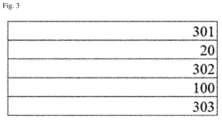
- FIG. 3 illustrates a modified structure where two protective films ( 301 , 302 ) exist on one side of the polarizing layer ( 100 ) and a reddening-resistant layer ( 20 ) exists between the protective films ( 301 , 302 ).
- a pressure-sensitive adhesive or an adhesive may be applied to the adhesion of the layer, where the reddening-resistant layer ( 20 ) may also be the pressure-sensitive adhesive or the adhesive.
- the details of the protective film ( 303 ) existing on the bottom of the polarizing layer ( 100 ) are the same as those of the protective film ( 302 ) existing on the bottom of the polarizing layer ( 100 ) in the structure of FIG. 2 .
- FIGS. 2 and 3 are exemplary embodiments of the present application, where the optical laminate of the present application may be composed of various structures in addition to these.
- the present application also relates to a display device comprising the optical laminate.
- the type of the display device may vary without particular limitation, which may be, for example, a known LCD (liquid crystal display) or OLED (organic light emitting display), and the like, and in such a display device, the optical laminate may be applied by a conventional method.
- Color coordinates were measured using a JASCO V-7100 spectrophotometer.
- the JASCO V-7100 spectrophotometer rotates the absorption axis of the measurement target polarizing plate from 0 degrees to 360 degrees with respect to the absorption axis of the polarizer built into the relevant instrument to measure the color coordinates (TD color coordinates) at the point where the transmittance is minimum and rotates the absorption axis of the measurement target polarizing plate 90 degrees clockwise again at the point where the transmittance is minimum to measure the color coordinates (MD color coordinates).
- the representative values of the color coordinates are derived based on the respective values measured by the spectrophotometer.
- Color coordinates described in the Examples of this application are color coordinates that are measured by the JASCO V-7100 spectrophotometer.
- the infrared reflectance of the reddening-resistant layer was confirmed by the following method.
- the infrared reflectance was evaluated in a state where a reddening-resistant layer was formed on a TAC (triacetyl cellulose) film having a thickness of approximately about 60 ⁇ m in the manner described in the following examples.
- the thickness of the reddening-resistant layer is described in each example.
- a black tape (TOMOEGAWA) was attached to the bottom (the surface of the film on which the reddening-resistant layer was not formed) of the TAC film in the laminate of the reddening-resistant layer/TAC film to perform darkening treatment.
- the refractive index and Cauchy parameter measurements of the reddening-resistant layer were performed in the following manner.
- the evaluation was performed in a state where the reddening-resistant layer was formed on a TAC (triacetyl cellulose) film having a thickness of approximately about 60 ⁇ m in the manner described in the following examples.
- the thickness of the reddening-resistant layer is described in each example.
- the characteristics were evaluated using a J. A. Woollam Co. M-2000 Ellipsometer.
- linearly polarized light was measured at a wavelength range of 380 nm to 1,000 nm at an incident angle of 70 degrees using the ellipsometer.
- the measured linearly polarized light data (ellipsometry data (Psi ( ⁇ ), delta ( ⁇ )) were subjected to fitting by using the Complete EASE software so that the MSE of the Cauchy model of Equation 1 was 25 or less, and to obtain the n ( ⁇ ), A, B and C value of Equation 6.
- the Roughness function was applied in the range of ⁇ 20 nm 50 nm.
- n ( ⁇ ) is the refractive index at a wavelength of ⁇ nm.
- the surface area ratio of the reddening-resistant layer (void-containing layer (porous layer)) was measured using an AFM (atomic force microscope, Park Systems, XE7).
- As a probe (tip) for the measurement PPP-NCHR 10 (Force Constant: 42 N/m, Resonance Frequency 330 kHz) was used. Measurement conditions were as follows:
- a reddening-resistant layer was produced by applying TMPTA (trimethylolpropane triacrylate) as a binder and applying hollow silica particles.
- TMPTA trimethylolpropane triacrylate
- hollow silica particles particles having D10, D50 and D90 particle diameters of 32.1 nm, 62.6 nm and 123.4 nm, respectively, were used.
- the average of the pore sizes measured by TEM was approximately 38.3 nm, and the particle diameter was approximately 53 nm.
- a polarizing plate was produced in the same manner as in Example 4, except that the reddening-resistant layer was not applied.
- a polarizing plate was produced in the same manner as in Example 1, except that the polarizing layer (B) of Production Example 2 was applied as the polarizing layer and a reddening-resistant layer having a thickness of about 500 nm was applied, which was formed by applying the coating material of the reddening-resistant layer of Production Example 5.
- the surface area ratio measured for the surface opposite to the surface of the formed reddening-resistant layer in contact with the TAC film was at a level of about 0.2207.
- a polarizing plate was produced in the same manner as in Example 6, except that the coating material for the reddening-resistant layer of Production Example 4 was applied.
- the surface area ratio measured on the surface opposite to the surface of the formed reddening-resistant layer in contact with the TAC film was at a level of about 0.0387.
- a polarizing plate was produced in the same manner as in Example 6, except that the coating material for the reddening-resistant layer of Production Example 3 was applied.
- the surface area ratio measured for the surface opposite to the surface of the formed reddening-resistant layer in contact with the TAC film was at a level of about 0.0513.
- a polarizing plate was produced in the same manner as in Example 6, except that a reddening-resistant layer having a thickness of about 3000 nm formed by applying the reddening-resistant layer material of Production Example 6 was applied as the reddening-resistant layer.
- the surface area ratio measured for the surface opposite to the surface of the formed reddening-resistant layer in contact with the TAC film was at a level of about 0.0611.
- a resin layer was formed on a TAC (triacetyl cellulose) film (Hyosung, PG601F) having a thickness of approximately 60 ⁇ m.
- the resin layer was formed by coating the resin layer (A) material of Production Example 7 with a Mayer bar, drying it at about 60° C. for about 1 minute, and then irradiating it with ultraviolet rays (252 mJ/cm 2 ) to have a final thickness of about 450 nm.
- the surface area ratio measured on the surface opposite to the surface of the formed resin layer in contact with the TAC film was in a level of about 0.01.
- a COP (cycloolefin polymer) film (manufacturer: Zeon) having a thickness of approximately 30 ⁇ m as a protective film was attached to the polarizing layer (A) obtained in Production Example 1 by applying a general optical water-based adhesive layer (thickness: 100 nm).
- the formed resin layer was attached to the polarizing layer (A) in the laminate of the COP film and the polarizing layer (A) as produced above with the same water-based adhesive agent (thickness: 100 nm) as above.
- an acrylic pressure-sensitive adhesive layer was formed on the bottom of the polarizing plate to produce a polarizing plate (optical laminate) having a structure in which the protective film (COP film), the adhesive layer, the polarizing layer, the adhesive layer, the resin layer, the protective film (TAC film) and the pressure-sensitive adhesive layer were sequentially laminated.
- a polarizing plate optical laminate having a structure in which the protective film (COP film), the adhesive layer, the polarizing layer, the adhesive layer, the resin layer, the protective film (TAC film) and the pressure-sensitive adhesive layer were sequentially laminated.
- the heat-proof test was performed for the Examples and Comparative Examples above, the single transmittance and color coordinate a* change amount were evaluated and the results are summarized and described in Table 2.
- the heat-proof test was performed by contacting the top and bottom whole surfaces of the polarizing plate produced in each of the Examples or Comparative Examples with soda lime glass (SEWON TECH) having a thickness of about 1.1 mm and laminating them, and then maintaining the resulting product at 105° C. for 250 hours.
- SEWON TECH soda lime glass
- the results were summarized as NG when it was confirmed and PASS when it was not confirmed, and described in Table 2 (in Table 2 below, the unit of transmittance is %):
Landscapes
- Physics & Mathematics (AREA)
- Chemical & Material Sciences (AREA)
- General Physics & Mathematics (AREA)
- Optics & Photonics (AREA)
- Organic Chemistry (AREA)
- Health & Medical Sciences (AREA)
- Polymers & Plastics (AREA)
- Medicinal Chemistry (AREA)
- Chemical Kinetics & Catalysis (AREA)
- Life Sciences & Earth Sciences (AREA)
- Engineering & Computer Science (AREA)
- Wood Science & Technology (AREA)
- Materials Engineering (AREA)
- Polarising Elements (AREA)
- Laminated Bodies (AREA)
- Surface Treatment Of Optical Elements (AREA)
- Devices For Indicating Variable Information By Combining Individual Elements (AREA)
- Optical Filters (AREA)
Abstract
Description
Δa*=a* a −a* i. [Equation 1]
ΔTs=T a −T i. [Equation 2]
1/(1+0.025d/R)=0.70 to 1.0. [Equation 3]
H L<0.9×H P. [Equation 4]
q=4π sin(θ/λ). [Equation 5]
q=4π sin(θ/λ). [Equation A]
-
- x-scan size: 1 μm
- y-scan size: 1 μm
- Scan rate: 0.7 to 1 Hz
- Z Servo Gain: 1
- Set Point: 10 to 15 nm
-
- Scope: Line
- Orientation: X and Y axis
- Regression Order: 1
| TABLE 1 | ||
| Reddening-resistant layer | ||
| IR | Scattering | Thermal | |||
| Cauchy Parameter coefficient | Reflectance | vector | diffusivity |
| A | B | C | (%) | (nm−1) | relative ratio | ||
| Example | 1 | 1.331 | 0.00287 | 0.000101 | 3.34 | 0.132 | 60% |
| 2 | 1.335 | 0.00363 | 0.000244 | 3.76 | 0.128 | 62% | |
| 3 | 1.332 | 0 | 0.000347 | 2.71 | 0.13 | 63% | |
| 4 | 1.333 | 0.000485 | 0.00025979 | 3.51 | 0.122 | 64% | |
| 5 | 1.332 | 0.00172 | 0.000301 | 3.4 | 0.123 | 60% | |
| 6 | 1.453 | 0.00319 | 0.000339 | 4.4 | 0.1 | 67% | |
| 7 | 1.401 | 0.00485 | 0.000025979 | 3.58 | 0.126 | 67% | |
| 8 | 1.315 | 0.000258 | 0.0000134 | 2.85 | 0.141 | 60% | |
| 9 | 1.489 | 0.000104 | 0.0000804 | 4.1 | 0.184 | 88% |
| Comparative Example 3 | 1.515 | 0.000864 | 0.0000151 | 1.8 | 0.211 | 92% |
| IR Reflectance: Infrared reflectance | ||||||
| Scattering vector: Scattering vector in which a peak is identified on a log value graph of scattering intensity of small angle X-ray scattering | ||||||
| Thermal diffusivity: Relative ratio of thermal diffusivity of reddening-resistant layer/TAC film laminate to thermal diffusivity of TAC film at 95° C. | ||||||
| TABLE 2 | |||
| Holding at 105° C. for 250 hours | |||
| a* | |||||||
| Initial | Naked | Transmittance | change |
| Transmittance | a* | Transmittance | a* | eye | change amount | amount | ||
| Example | 1 | 41.3 | −1.47 | 40 | −0.87 | PASS | −1.3 | 0.6 |
| 2 | 41.5 | −2.05 | 40.6 | −1.95 | PASS | −0.9 | 0.1 | |
| 3 | 41.3 | −1.66 | 40.5 | −1.56 | PASS | −0.8 | 0.1 | |
| 4 | 41.5 | −3.1 | 41.2 | −1.9 | PASS | −0.3 | 1.2 | |
| 5 | 41.6 | −3.4 | 40.6 | −2.4 | PASS | −1 | 1 | |
| 6 | 41.4 | −1.88 | 41.8 | −2 | PASS | 0.4 | −0.12 | |
| 7 | 41.1 | −2.01 | 41.5 | −2.03 | PASS | 0.4 | −0.02 | |
| 8 | 40.7 | −1.93 | 41.9 | −2.08 | PASS | 1.2 | −0.15 | |
| 9 | 41.3 | −1.94 | 42 | −2.14 | PASS | 0.7 | −0.2 | |
| Comparative | 1 | 41.8 | −1.8 | 31.8 | 2 | NG | −10 | 3.8 |
| Example | 2 | 41.3 | −3.4 | 31.3 | 3.2 | NG | −10 | 6.6 |
| 3 | 41.7 | −2.7 | 32.9 | 2.5 | NG | −8.8 | 5.2 | |
Claims (10)
Applications Claiming Priority (3)
| Application Number | Priority Date | Filing Date | Title |
|---|---|---|---|
| KR10-2019-0037455 | 2019-03-29 | ||
| KR20190037455 | 2019-03-29 | ||
| PCT/KR2020/001460 WO2020204332A1 (en) | 2019-03-29 | 2020-01-31 | Optical laminate |
Publications (2)
| Publication Number | Publication Date |
|---|---|
| US20220171111A1 US20220171111A1 (en) | 2022-06-02 |
| US12337583B2 true US12337583B2 (en) | 2025-06-24 |
Family
ID=72667315
Family Applications (1)
| Application Number | Title | Priority Date | Filing Date |
|---|---|---|---|
| US17/598,134 Active 2040-12-22 US12337583B2 (en) | 2019-03-29 | 2020-01-31 | Optical laminate |
Country Status (7)
| Country | Link |
|---|---|
| US (1) | US12337583B2 (en) |
| EP (1) | EP3950306B1 (en) |
| JP (1) | JP7335047B2 (en) |
| KR (1) | KR102477367B1 (en) |
| CN (1) | CN113631366B9 (en) |
| TW (1) | TWI739293B (en) |
| WO (1) | WO2020204332A1 (en) |
Families Citing this family (4)
| Publication number | Priority date | Publication date | Assignee | Title |
|---|---|---|---|---|
| KR102344867B1 (en) * | 2019-03-29 | 2021-12-30 | 주식회사 엘지화학 | Optical Laminate |
| US12124068B2 (en) * | 2019-03-29 | 2024-10-22 | Lg Chem, Ltd. | Reddening-resistant layer |
| CN113613881A (en) * | 2019-03-29 | 2021-11-05 | 株式会社Lg化学 | Optical laminate |
| JP7415234B2 (en) * | 2019-03-29 | 2024-01-17 | エルジー・ケム・リミテッド | optical laminate |
Citations (24)
| Publication number | Priority date | Publication date | Assignee | Title |
|---|---|---|---|---|
| WO2001048517A1 (en) | 1999-12-28 | 2001-07-05 | Gunze Co., Ltd | Polarizing plate |
| KR20050036458A (en) | 2003-10-16 | 2005-04-20 | 삼성에스디아이 주식회사 | Plasma display device |
| JP2005321593A (en) | 2004-05-10 | 2005-11-17 | Nitto Denko Corp | Liquid crystal display device and heat insulating sheet |
| KR20060051782A (en) | 2004-09-28 | 2006-05-19 | 후지 샤신 필름 가부시기가이샤 | Manufacturing method of antireflection film, antireflection film, polarizing plate using the same, and image display device using them |
| WO2010095447A1 (en) | 2009-02-20 | 2010-08-26 | 日本化薬株式会社 | Dye-containing polarizing plate having cured resin layer |
| JP2010256625A (en) | 2009-04-24 | 2010-11-11 | Nippon Zeon Co Ltd | Insulation material |
| JP2011118135A (en) | 2009-12-03 | 2011-06-16 | Fujifilm Corp | Polarizing plate protective film, polarizing plate, and liquid crystal display device |
| KR20130025321A (en) | 2011-09-01 | 2013-03-11 | 동우 화인켐 주식회사 | A polarizing plate and liquid crystal display comprising the same |
| US20130141787A1 (en) | 2011-12-02 | 2013-06-06 | Pil Joo Kim | Polarizer having high durability and method of fabricating the same |
| CN103299217A (en) | 2011-01-14 | 2013-09-11 | 大日本印刷株式会社 | Anti-reflective film, anti-reflective film production method, polarization plate and image display device |
| US20140184994A1 (en) * | 2012-05-31 | 2014-07-03 | Dai Nippon Printing Co., Ltd. | Optical layered body, polarizer, method for producing polarizer, image display device, method for producing image display device, and method for improving visibility of image display device |
| KR20140085292A (en) | 2012-12-27 | 2014-07-07 | 제일모직주식회사 | Transparent conductor and apparatus comprising the same |
| WO2015037869A1 (en) | 2013-09-11 | 2015-03-19 | 동우 화인켐 주식회사 | Low-reflective optical laminate |
| WO2017057256A1 (en) | 2015-09-30 | 2017-04-06 | 富士フイルム株式会社 | Laminate, polarizing plate, and image display device |
| JP2017075986A (en) | 2015-10-13 | 2017-04-20 | 株式会社サンリッツ | Polarizing plate with pressure-sensitive adhesive layer, method for producing the same, active energy ray-curable polymer composition used for the production, and liquid crystal display device |
| KR20170106920A (en) | 2016-03-14 | 2017-09-22 | 주식회사 엘지화학 | Anti-reflective film |
| KR20170129669A (en) | 2016-03-11 | 2017-11-27 | 주식회사 엘지화학 | Anti-refractive film |
| KR20170130780A (en) | 2016-05-19 | 2017-11-29 | 동우 화인켐 주식회사 | Polarizing plate |
| EP3251832A1 (en) * | 2016-03-09 | 2017-12-06 | LG Chem, Ltd. | Anti-reflection film |
| KR20180033016A (en) | 2016-09-23 | 2018-04-02 | 삼성에스디아이 주식회사 | Flexible display apparatus |
| JP2018180518A (en) | 2017-04-07 | 2018-11-15 | 住友化学株式会社 | Polarizer |
| JP2018200463A (en) | 2017-05-09 | 2018-12-20 | 日東電工株式会社 | Composition for optical members, optical member and image display device |
| JP2018205464A (en) | 2017-06-01 | 2018-12-27 | 株式会社サンリッツ | Polarizing plate and image display device |
| JP2019028196A (en) | 2017-07-28 | 2019-02-21 | 株式会社サンリッツ | Polarizing plate and image display device |
Family Cites Families (4)
| Publication number | Priority date | Publication date | Assignee | Title |
|---|---|---|---|---|
| JP4622472B2 (en) | 2004-11-16 | 2011-02-02 | コニカミノルタオプト株式会社 | Antiglare antireflection film, method for producing antiglare antireflection film, polarizing plate and display device |
| KR20170086961A (en) * | 2016-01-19 | 2017-07-27 | 주식회사 엘지화학 | Protective optical film for polarizing plate and polarizing plate and liquid crystal display comprising the same |
| KR102050625B1 (en) * | 2016-08-31 | 2019-11-29 | 주식회사 엘지화학 | Optical film and polarizing plate comprising the same |
| KR102037468B1 (en) | 2017-09-29 | 2019-11-26 | (주) 가성팩 | Packaging apparatus |
-
2020
- 2020-01-31 EP EP20781780.0A patent/EP3950306B1/en active Active
- 2020-01-31 US US17/598,134 patent/US12337583B2/en active Active
- 2020-01-31 WO PCT/KR2020/001460 patent/WO2020204332A1/en not_active Ceased
- 2020-01-31 JP JP2021556567A patent/JP7335047B2/en active Active
- 2020-01-31 KR KR1020200011935A patent/KR102477367B1/en active Active
- 2020-01-31 CN CN202080023610.7A patent/CN113631366B9/en active Active
- 2020-02-03 TW TW109103219A patent/TWI739293B/en active
Patent Citations (31)
| Publication number | Priority date | Publication date | Assignee | Title |
|---|---|---|---|---|
| WO2001048517A1 (en) | 1999-12-28 | 2001-07-05 | Gunze Co., Ltd | Polarizing plate |
| KR20050036458A (en) | 2003-10-16 | 2005-04-20 | 삼성에스디아이 주식회사 | Plasma display device |
| JP2005321593A (en) | 2004-05-10 | 2005-11-17 | Nitto Denko Corp | Liquid crystal display device and heat insulating sheet |
| KR20060051782A (en) | 2004-09-28 | 2006-05-19 | 후지 샤신 필름 가부시기가이샤 | Manufacturing method of antireflection film, antireflection film, polarizing plate using the same, and image display device using them |
| WO2010095447A1 (en) | 2009-02-20 | 2010-08-26 | 日本化薬株式会社 | Dye-containing polarizing plate having cured resin layer |
| JP2010256625A (en) | 2009-04-24 | 2010-11-11 | Nippon Zeon Co Ltd | Insulation material |
| JP2011118135A (en) | 2009-12-03 | 2011-06-16 | Fujifilm Corp | Polarizing plate protective film, polarizing plate, and liquid crystal display device |
| CN103299217A (en) | 2011-01-14 | 2013-09-11 | 大日本印刷株式会社 | Anti-reflective film, anti-reflective film production method, polarization plate and image display device |
| US20130329297A1 (en) * | 2011-01-14 | 2013-12-12 | Dai Nippon Printing Co., Ltd. | Antireflection film, method for producing antireflection film, polarizer and image display device |
| KR20140006876A (en) | 2011-01-14 | 2014-01-16 | 다이니폰 인사츠 가부시키가이샤 | Anti-reflective film, anti-reflective film production method, polarization plate and image display device |
| TWI515271B (en) | 2011-01-14 | 2016-01-01 | Dainippon Printing Co Ltd | Anti-reflection film, anti-reflection film manufacturing method, polarizing film and image display device |
| KR20130025321A (en) | 2011-09-01 | 2013-03-11 | 동우 화인켐 주식회사 | A polarizing plate and liquid crystal display comprising the same |
| US20130141787A1 (en) | 2011-12-02 | 2013-06-06 | Pil Joo Kim | Polarizer having high durability and method of fabricating the same |
| US20140184994A1 (en) * | 2012-05-31 | 2014-07-03 | Dai Nippon Printing Co., Ltd. | Optical layered body, polarizer, method for producing polarizer, image display device, method for producing image display device, and method for improving visibility of image display device |
| KR20140085292A (en) | 2012-12-27 | 2014-07-07 | 제일모직주식회사 | Transparent conductor and apparatus comprising the same |
| WO2015037869A1 (en) | 2013-09-11 | 2015-03-19 | 동우 화인켐 주식회사 | Low-reflective optical laminate |
| WO2017057256A1 (en) | 2015-09-30 | 2017-04-06 | 富士フイルム株式会社 | Laminate, polarizing plate, and image display device |
| JP2017075986A (en) | 2015-10-13 | 2017-04-20 | 株式会社サンリッツ | Polarizing plate with pressure-sensitive adhesive layer, method for producing the same, active energy ray-curable polymer composition used for the production, and liquid crystal display device |
| TWI627435B (en) | 2016-03-09 | 2018-06-21 | 南韓商Lg化學股份有限公司 | Anti-reflection film |
| EP3251832A1 (en) * | 2016-03-09 | 2017-12-06 | LG Chem, Ltd. | Anti-reflection film |
| CN107635765A (en) | 2016-03-09 | 2018-01-26 | 株式会社Lg化学 | Anti-reflection film |
| JP2018533762A (en) | 2016-03-09 | 2018-11-15 | エルジー・ケム・リミテッド | Antireflective film |
| KR20170129669A (en) | 2016-03-11 | 2017-11-27 | 주식회사 엘지화학 | Anti-refractive film |
| KR20180029015A (en) | 2016-03-11 | 2018-03-19 | 주식회사 엘지화학 | Anti-refractive film |
| KR20170106920A (en) | 2016-03-14 | 2017-09-22 | 주식회사 엘지화학 | Anti-reflective film |
| KR20170130780A (en) | 2016-05-19 | 2017-11-29 | 동우 화인켐 주식회사 | Polarizing plate |
| KR20180033016A (en) | 2016-09-23 | 2018-04-02 | 삼성에스디아이 주식회사 | Flexible display apparatus |
| JP2018180518A (en) | 2017-04-07 | 2018-11-15 | 住友化学株式会社 | Polarizer |
| JP2018200463A (en) | 2017-05-09 | 2018-12-20 | 日東電工株式会社 | Composition for optical members, optical member and image display device |
| JP2018205464A (en) | 2017-06-01 | 2018-12-27 | 株式会社サンリッツ | Polarizing plate and image display device |
| JP2019028196A (en) | 2017-07-28 | 2019-02-21 | 株式会社サンリッツ | Polarizing plate and image display device |
Also Published As
| Publication number | Publication date |
|---|---|
| JP7335047B2 (en) | 2023-08-29 |
| CN113631366B9 (en) | 2023-12-05 |
| WO2020204332A1 (en) | 2020-10-08 |
| EP3950306A4 (en) | 2022-05-04 |
| JP2022526749A (en) | 2022-05-26 |
| CN113631366A (en) | 2021-11-09 |
| EP3950306B1 (en) | 2024-10-30 |
| EP3950306A1 (en) | 2022-02-09 |
| US20220171111A1 (en) | 2022-06-02 |
| KR20200115080A (en) | 2020-10-07 |
| TWI739293B (en) | 2021-09-11 |
| TW202045959A (en) | 2020-12-16 |
| KR102477367B1 (en) | 2022-12-15 |
| CN113631366B (en) | 2023-10-27 |
Similar Documents
| Publication | Publication Date | Title |
|---|---|---|
| US12337583B2 (en) | Optical laminate | |
| US12083771B2 (en) | Optical laminate | |
| US12216300B2 (en) | Optical laminate comprising an optical functional layer and a porous layer | |
| US12397527B2 (en) | Optical laminate | |
| US12025822B2 (en) | Reddening-resistant layer | |
| US12130456B2 (en) | Optical laminate | |
| US12019256B2 (en) | Optical laminate | |
| US12253703B2 (en) | Reddening-resistant layer | |
| US20220163749A1 (en) | Display device | |
| US12202230B2 (en) | Reddening-resistant layer | |
| US12124067B2 (en) | Optical laminate including reddening-resistant layer | |
| US12124068B2 (en) | Reddening-resistant layer | |
| US12204127B2 (en) | Optical laminate |
Legal Events
| Date | Code | Title | Description |
|---|---|---|---|
| AS | Assignment |
Owner name: LG CHEM, LTD., KOREA, REPUBLIC OF Free format text: ASSIGNMENT OF ASSIGNORS INTEREST;ASSIGNORS:SHIN, NA YOUNG;RAH, KYUN IL;BYUN, JIN SEOK;AND OTHERS;SIGNING DATES FROM 20210820 TO 20210915;REEL/FRAME:057595/0116 |
|
| FEPP | Fee payment procedure |
Free format text: ENTITY STATUS SET TO UNDISCOUNTED (ORIGINAL EVENT CODE: BIG.); ENTITY STATUS OF PATENT OWNER: LARGE ENTITY |
|
| STPP | Information on status: patent application and granting procedure in general |
Free format text: DOCKETED NEW CASE - READY FOR EXAMINATION |
|
| STPP | Information on status: patent application and granting procedure in general |
Free format text: NON FINAL ACTION MAILED |
|
| STPP | Information on status: patent application and granting procedure in general |
Free format text: RESPONSE TO NON-FINAL OFFICE ACTION ENTERED AND FORWARDED TO EXAMINER |
|
| STPP | Information on status: patent application and granting procedure in general |
Free format text: FINAL REJECTION MAILED |
|
| STPP | Information on status: patent application and granting procedure in general |
Free format text: DOCKETED NEW CASE - READY FOR EXAMINATION |
|
| STPP | Information on status: patent application and granting procedure in general |
Free format text: NON FINAL ACTION MAILED |
|
| STPP | Information on status: patent application and granting procedure in general |
Free format text: RESPONSE TO NON-FINAL OFFICE ACTION ENTERED AND FORWARDED TO EXAMINER |
|
| STPP | Information on status: patent application and granting procedure in general |
Free format text: NOTICE OF ALLOWANCE MAILED -- APPLICATION RECEIVED IN OFFICE OF PUBLICATIONS |
|
| STPP | Information on status: patent application and granting procedure in general |
Free format text: RESPONSE TO NON-FINAL OFFICE ACTION ENTERED AND FORWARDED TO EXAMINER |
|
| STPP | Information on status: patent application and granting procedure in general |
Free format text: NOTICE OF ALLOWANCE MAILED -- APPLICATION RECEIVED IN OFFICE OF PUBLICATIONS |
|
| AS | Assignment |
Owner name: SHANJIN OPTOELECTRONICS (SUZHOU) CO., LTD., CHINA Free format text: ASSIGNMENT OF ASSIGNORS INTEREST;ASSIGNOR:LG CHEM LTD.;REEL/FRAME:070629/0264 Effective date: 20250317 |
|
| STCF | Information on status: patent grant |
Free format text: PATENTED CASE |