US12308899B2 - Composite coil pattern for wireless charging and magnetic secure transmission - Google Patents
Composite coil pattern for wireless charging and magnetic secure transmission Download PDFInfo
- Publication number
- US12308899B2 US12308899B2 US17/342,028 US202117342028A US12308899B2 US 12308899 B2 US12308899 B2 US 12308899B2 US 202117342028 A US202117342028 A US 202117342028A US 12308899 B2 US12308899 B2 US 12308899B2
- Authority
- US
- United States
- Prior art keywords
- coil
- line
- pattern
- lines
- wireless charging
- Prior art date
- Legal status (The legal status is an assumption and is not a legal conclusion. Google has not performed a legal analysis and makes no representation as to the accuracy of the status listed.)
- Active, expires
Links
Images


Classifications
-
- H—ELECTRICITY
- H01—ELECTRIC ELEMENTS
- H01F—MAGNETS; INDUCTANCES; TRANSFORMERS; SELECTION OF MATERIALS FOR THEIR MAGNETIC PROPERTIES
- H01F27/00—Details of transformers or inductances, in general
- H01F27/28—Coils; Windings; Conductive connections
-
- H—ELECTRICITY
- H04—ELECTRIC COMMUNICATION TECHNIQUE
- H04B—TRANSMISSION
- H04B5/00—Near-field transmission systems, e.g. inductive or capacitive transmission systems
- H04B5/70—Near-field transmission systems, e.g. inductive or capacitive transmission systems specially adapted for specific purposes
- H04B5/79—Near-field transmission systems, e.g. inductive or capacitive transmission systems specially adapted for specific purposes for data transfer in combination with power transfer
-
- H—ELECTRICITY
- H01—ELECTRIC ELEMENTS
- H01F—MAGNETS; INDUCTANCES; TRANSFORMERS; SELECTION OF MATERIALS FOR THEIR MAGNETIC PROPERTIES
- H01F27/00—Details of transformers or inductances, in general
- H01F27/28—Coils; Windings; Conductive connections
- H01F27/30—Fastening or clamping coils, windings, or parts thereof together; Fastening or mounting coils or windings on core, casing, or other support
- H01F27/303—Clamping coils, windings or parts thereof together
-
- H—ELECTRICITY
- H01—ELECTRIC ELEMENTS
- H01Q—ANTENNAS, i.e. RADIO AERIALS
- H01Q1/00—Details of, or arrangements associated with, antennas
- H01Q1/12—Supports; Mounting means
- H01Q1/22—Supports; Mounting means by structural association with other equipment or articles
- H01Q1/2208—Supports; Mounting means by structural association with other equipment or articles associated with components used in interrogation type services, i.e. in systems for information exchange between an interrogator/reader and a tag/transponder, e.g. in Radio Frequency Identification [RFID] systems
- H01Q1/2225—Supports; Mounting means by structural association with other equipment or articles associated with components used in interrogation type services, i.e. in systems for information exchange between an interrogator/reader and a tag/transponder, e.g. in Radio Frequency Identification [RFID] systems used in active tags, i.e. provided with its own power source or in passive tags, i.e. deriving power from RF signal
-
- H—ELECTRICITY
- H02—GENERATION; CONVERSION OR DISTRIBUTION OF ELECTRIC POWER
- H02J—CIRCUIT ARRANGEMENTS OR SYSTEMS FOR SUPPLYING OR DISTRIBUTING ELECTRIC POWER; SYSTEMS FOR STORING ELECTRIC ENERGY
- H02J50/00—Circuit arrangements or systems for wireless supply or distribution of electric power
- H02J50/10—Circuit arrangements or systems for wireless supply or distribution of electric power using inductive coupling
Definitions
- One or more embodiments relate to a composite coil pattern for wireless charging and magnetic secure transmission (MST).
- Wireless charging which has been recently applied to smartphones, uses a coil-type antenna to transmit and receive magnetic fields. Because near field communication (NFC) antennas for communication and magnetic secure transmission (MST) antennas for electronic payments are coils that use a magnetic field, both need to be complexly designed together with a wireless charging coil within a limited area.
- NFC near field communication
- MST magnetic secure transmission
- the wireless charging coil because the induced current must be transmitted to a circuit without loss to receive wireless power, performance is improved as low resistance characteristics are secured. In contrast, in the case of the MST coil, if a predetermined resistance value or more is not secured, the current increases rapidly, and the circuit or coil may not withstand the internal pressure and be damaged.
- One or more embodiments include a coil pattern designed for achieving different functions of wireless charging and a magnetic secure transmission (MST) using one coil within a limited area.
- MST magnetic secure transmission
- a composite coil pattern for wireless charging and magnetic security transmission includes: a first terminal, a second terminal, a coil connecting the first terminal to the second terminal; and a magnetic security transmission (MST) pattern portion connected to the coil through a connection line branching from an outer periphery of the coil, wherein the MST pattern portion is at one side in a direction with respect to the coil, the MST pattern portion includes a plurality of lines parallel to the direction, the plurality of lines connect an inner end located close to the coil and an outer end located far from the coil, and when an inner end of a first line from among the plurality of lines and an inner end of a second line next to the first line are connected to each other, an outer end of the second line and an outer end of a third line next to the second line are connected to each other, so that the plurality of lines are connected in series.
- MST magnetic security transmission
- an inner end of the third line and an inner end of a fourth line next to the third line may be connected to each other.
- At least one inner end of each of the plurality of lines may be located along an outer periphery of the coil.
- the inner end and the outer end may be bent to be connected to adjacent lines.
- one end of the MST pattern portion may be connected to the connection line branching from the outer periphery line of the coil, and the other end of the MST pattern portion may form a third terminal, and the third terminal may be at an outer periphery of the MST pattern portion.
- the first terminal may be selectively used as an input terminal for wireless charging or an input terminal for MST
- the second terminal may be an output terminal for wireless charging
- the third terminal may be an output terminal for MST.
- both the coil and the MST pattern portion may be on the same plane, and outer ends of the plurality of lines may be formed on the same plane and formed perpendicular to the direction.
- the width of the plurality of lines may be less than the width of the coil, and the width of the inner end and the outer end may be wider than the width of the plurality of lines.
- FIG. 1 shows a general coil pattern 500 for wireless charging and magnetic secure transition (MST);
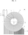
- FIG. 2 shows a composite coil pattern 100 for wireless charging and MST according to an embodiment
- FIGS. 3 and 4 are enlarged views of the composite coil pattern 100 for wireless charging and MST illustrated in FIG. 2 .
- FIG. 1 shows a general coil pattern 500 for wireless charging and magnetic secure transition (MST).
- MST magnetic secure transition
- the general coil pattern 500 for wireless charging and MST may include a wireless charging coil 50 and an MST coil 60 .
- the wireless charging coil 50 may connect a first terminal 51 to a second terminal 52 .
- the wireless charging coil 50 may be a pattern line wound a plurality of times.
- the MST coil 60 may be connected to the wireless charging coil 50 through a connection line branching from the outer periphery of the wireless charging coil 50 .
- the MST coil 60 connected to the connection line may form a wound pattern separately from the wireless charging coil 50 in the vicinity of the wireless charging coil 50 .
- the MST coil 60 may be a spiral wound pattern, and the wireless charging coil 50 and the MST coil 60 may form different spiral patterns from each other.
- the center of the spiral of the wireless charging coil 50 and the center of the spiral of the MST coil 60 may be different from each other.
- One end of the MST coil 60 may be connected to the connection line branching from the outer periphery line of the wireless charging coil 50 , and the other end of the MST coil 60 may be connected to a third terminal 53 .
- the first terminal 51 may be used as an input terminal and the second terminal 52 may be used as an output terminal.
- the first terminal 51 may be used as an input terminal and the third terminal 53 may be used as an output terminal.
- the first terminal 51 may be selectively used as an input terminal for wireless charging and an input terminal for MST
- the second terminal 52 may be an output terminal for wireless charging
- the third terminal 53 may be an output terminal for MST.
- a separate MST coil 60 of a spiral pattern through a connection line branching from the outer periphery line of a wireless charging coil 50 , an additionally increased resistance value may be secured in an MST operation.
- the wireless charging operation only the first terminal 51 , the second terminal 52 , and the wireless charging coil 50 may be used to form a low resistance value, and in the MST operation, by using the first terminal 51 and the third terminal 53 , the wireless charging coil 50 and the MST coil 60 may be simultaneously used to form a high resistance value.
- a region in which the magnetic field is offset may occur. For example, between the wireless charging coil 50 region and the MST coil 60 region, a region in which a first magnetic field generated by the wireless charging coil 50 and a second magnetic field generated by the MST coil 60 may be offset from each other may occur. For example, when a credit card payment is performed, a region in which a magnetic reader of a POS terminal cannot recognize the payment information may occur.
- the MST coil 60 is formed in a spiral pattern, an empty space may inevitably be generated inside the spiral pattern, and accordingly, there may be inefficiency in securing a maximum length of lines within a limited area.
- it is advantageous to reduce the general space occupied by the coil pattern 500 and because the MST coil 60 is provided to secure the required resistance value during the MST operation, the space as much as the empty space inside the MST coil 60 may be wasted.
- the MST coil 60 is formed in a spiral pattern, the third terminal 53 connected to the MST coil 60 may inevitably be present in the spiral pattern. Therefore, in order to electrically connect the third terminal 53 to the outside of the MST coil 60 , a separate layer or a separate lead line may be required.
- FIG. 2 shows a composite coil pattern 100 for wireless charging and MST according to an embodiment.
- FIGS. 3 and 4 are enlarged views of the composite coil pattern 100 for wireless charging and MST illustrated in FIG. 2 .
- the composite coil pattern 100 may solve the problem in which a magnetic field is offset in previous methods.
- the composite coil pattern 100 according to an embodiment may have a structure capable of securing a sufficient resistance value required for the MST operation in a smaller area than the previous method (the coil pattern 500 ).
- the composite coil pattern 100 for wireless charging and MST may include a wireless charging coil portion 10 and an MST pattern portion 20 .
- the wireless charging coil portion 10 may include a first terminal 11 , a second terminal 12 , and a wireless charging coil (i.e., coil pattern 15 ) connecting the first terminal 11 to the second terminal 12 .
- the wireless charging coil pattern 15 may connect the first terminal 11 to the second terminal 12 , and may be a pattern line wound a plurality of times.
- the MST pattern portion 20 may be connected to the wireless charging coil pattern 15 through a connection line 31 branching from the outer periphery of the wireless charging coil pattern 15 .
- the MST pattern portion 20 may be located in a direction 30 with respect to the wireless charging coil pattern 15 .
- the MST pattern portion 20 may form a separate pattern from the wireless charging coil pattern 15 .
- the MST pattern portion 20 may include a plurality of lines 25 including first to fourth lines 25 - 1 to 25 - 4 parallel to the direction 30 .
- the direction 30 may be a direction towards which the MST pattern portion 20 is directed with respect to the wireless charging coil portion 10 , that is, a direction in which the MST pattern portion 20 is located with respect to the wireless charging coil portion 10 .
- Each of the plurality of first to fourth lines 25 - 1 , 25 - 2 , 25 - 3 and 25 - 4 included in the MST pattern portion 20 may be parallel to the direction 30 .
- the plurality of lines 25 may be lines connecting an inner end 21 located close to the wireless charging coil portion 10 and an outer end 22 located far from the wireless charging coil portion 10 .
- the direction 30 may correspond to a direction from the inner end 21 to the outer end 22 with respect to each of the plurality of lines 25 .
- the plurality of lines 25 included in the MST pattern portion 20 may be connected in series. Referring to FIG. 4 , details of the above description are as below. When any one of the first line 25 - 1 and the second line 25 - 2 next to the first line 25 - 1 from among the plurality of lines 25 are connected at the inner end 21 , the second line 25 - 2 and the third line 25 - 3 next to the second line 25 - 2 may be connected at the outer end 22 , and when the second line 25 - 2 and the third line 25 - 3 are connected at the outer end 22 , the third line 25 - 3 and the fourth line 25 - 4 next to the third line 25 - 3 may be connected at the inner end 21 , so that the plurality of lines 25 are connected in series.
- the outer end 22 of the second line 25 - 2 and the outer end 22 of the third line 25 - 3 next to the second line 25 - 2 may be connected to each other, so that the plurality of lines 25 are connected in series.
- the inner end 21 of the third line 25 - 3 and the inner end 21 of the fourth line 25 - 4 next to the third line 25 - 3 may be connected to each other, so that the plurality of lines 25 are connected in series.
- the line (e.g., 25 - 1 , 25 - 2 , 25 - 3 , and 25 - 4 ) forming the MST pattern portion 20 may be in a meander or zigzag shape.
- the plurality of lines 25 may be parallel to each other except for parts where adjacent lines are connected to each other (i.e., a curved part, the inner end 21 , and the outer end 22 ).
- the plurality of lines in the meander or zigzag form may be straight lines and may be arranged in parallel with the direction 30 toward which the MST pattern portion 20 is directed with respect to the wireless charging coil portion 10 .
- One end of the MST pattern portion 20 may be connected to the connection line 31 branching from the outer periphery line of the wireless charging coil pattern 15 , and the other end of the MST pattern portion 20 may be connected to a third terminal 13 .
- the composite coil pattern 100 may use the first terminal 11 as an input terminal and the second terminal 12 as an output terminal during a wireless charging operation.
- the composite coil pattern 100 may use the first terminal 11 as an input terminal and the third terminal 13 as an output terminal during an MST operation.
- the first terminal 11 may be selectively used as an input terminal for wireless charging and an input terminal for MST
- the second terminal 12 may be an output terminal for wireless charging
- the third terminal 13 may be an output terminal for MST.
- the composite coil pattern 100 by additionally extending and forming the MST pattern portion 20 through the connection line 31 branching from the outer periphery line of the wireless charging coil pattern 15 , an additional increased resistance value may be secured in the MST operation.
- the wireless charging operation only the first terminal 11 , the second terminal 12 , and the wireless charging coil pattern 15 may be used to form a low resistance value, and in the MST operation, by using the first terminal 11 and the third terminal 13 , the wireless charging coil pattern 15 and the MST pattern 20 may be simultaneously used to form a high resistance value.
- the MST pattern portion 20 may be formed as described above in the composite coil pattern 100 according to an embodiment. Accordingly, the length of the line of the MST pattern portion 20 may be maximized in a smaller area than an existing coil pattern (e.g., the coil pattern 500 ), without an empty space. Therefore, the composite coil pattern 100 may secure an additional resistance value in a smaller area than an existing coil pattern (e.g., the coil pattern 500 ).
- the third terminal 13 may be at an outer periphery of the MST pattern portion 20 . Therefore, unlike the coil patterns of the related art (e.g., the coil pattern 500 ), in the composite coil pattern 100 , a lead line using a separate layer may not need to be formed to electrically connect the third terminal 13 to an external circuit (not shown).
- the MST pattern portion 20 is not a spiral structure, a problem in which the magnetic field is offset as in previous methods may not occur.
- the MST coil 60 is formed in a spiral pattern in the general coil pattern 500 , a region in which the first magnetic field generated by the wireless charging spiral coil 50 and the second magnetic field generated by the MST coil 60 of a spiral shape are offset from each other may occur.
- the MST pattern portion 20 is formed in a meander shape as described above, a side effect of the magnetic fields generated by the wireless charging coil portion 10 and the MST pattern portion 20 being offset from each other may be minimized.
- a magnetic field generated in a straight line section may be in an opposite direction to a magnetic field generated in a very next straight line section. That is, a direction of the magnetic field generated by the first line 25 - 1 may be the opposite to a direction of the magnetic field generated by the second line 25 - 2 , and a direction of the magnetic field generated by the second line 25 - 2 may be the opposite to a direction of the magnetic field generated by the third line 25 - 3 . Therefore, the magnetic fields generated by the plurality of straight lines 25 in the left and right directions may offset each other. Thus, the net magnetic field in the left and right directions generated by the MST pattern portion 20 may correspond to approximately 0.
- the magnetic field generated by the plurality of straight lines 25 is substantially perpendicular to the magnetic field generated by the wireless charging coil pattern 15 , a probability in which the magnetic fields generated by the plurality of straight lines 25 offset the magnetic field generated by the wireless charging coil pattern 15 may be significantly reduced. For example, in the MST operation, the degree of a magnetic field generated by the wireless charging coil pattern 15 and a magnetic field generated by the plurality of straight lines 25 offsetting each other may be minimized.
- the inner end 21 and the outer end 21 excluding the straight section may generate a net magnetic field.
- Current may flow in the same direction on the inner end 21 and the outer end 22 of the plurality of lines 25 , and the direction may be the same as the direction in which current flows in the wireless charging coil pattern 15 . Therefore, the net magnetic field generated by the plurality of inner ends 21 may reinforce the magnetic field generated by the wireless charging coil pattern 15 .
- the net magnetic field generated by the plurality of outer ends 22 may reinforce the magnetic field generated by the wireless charging coil pattern 15 . Therefore, the MST pattern portion 20 may generate the effect of having two or more windings at the outer periphery of the wireless charging coil pattern 15 .
- At least one of the inner ends 21 of the plurality of lines included in the MST pattern portion 20 may be located along the outer periphery of the wireless charging coil pattern 15 . That is, the at least one of the plurality of inner ends 21 of the plurality of lines 25 may be arranged to correspond to the outer periphery of the wireless charging coil pattern 15 , to provide an effect of further winding at the outer periphery of the wireless charging coil pattern 15 .
- the MST pattern portion 20 may be designed to satisfy a required resistance value or more for a minimum region.
- the width of the plurality of lines 25 may be less than the width of the wireless charging coil pattern 15 .
- the width of the inner end 21 and the outer end 22 may be wider than the width of the plurality of lines 25 .
- the width of the inner end 21 and the outer end 22 may correspond to the width of the wireless charging coil pattern 15 .
- embodiments of the disclosure are not limited thereto.
- different functions of wireless charging and an MST may be achieved using one coil within a limited area.
Landscapes
- Engineering & Computer Science (AREA)
- Power Engineering (AREA)
- Computer Networks & Wireless Communication (AREA)
- Signal Processing (AREA)
- Charge And Discharge Circuits For Batteries Or The Like (AREA)
Abstract
Description
Claims (20)
Applications Claiming Priority (4)
| Application Number | Priority Date | Filing Date | Title |
|---|---|---|---|
| KR10-2020-0089851 | 2020-07-20 | ||
| KR20200089851 | 2020-07-20 | ||
| KR1020200126380A KR102488576B1 (en) | 2020-07-20 | 2020-09-28 | Composite coil pattern for wireless charging and magnetic secure transmission |
| KR10-2020-0126380 | 2020-09-28 |
Publications (2)
| Publication Number | Publication Date |
|---|---|
| US20220021415A1 US20220021415A1 (en) | 2022-01-20 |
| US12308899B2 true US12308899B2 (en) | 2025-05-20 |
Family
ID=79292923
Family Applications (1)
| Application Number | Title | Priority Date | Filing Date |
|---|---|---|---|
| US17/342,028 Active 2042-12-16 US12308899B2 (en) | 2020-07-20 | 2021-06-08 | Composite coil pattern for wireless charging and magnetic secure transmission |
Country Status (2)
| Country | Link |
|---|---|
| US (1) | US12308899B2 (en) |
| CN (1) | CN113963911B (en) |
Citations (10)
| Publication number | Priority date | Publication date | Assignee | Title |
|---|---|---|---|---|
| US20080315311A1 (en) * | 2007-06-22 | 2008-12-25 | Semiconductor Energy Laboratory Co., Ltd. | Semiconductor device |
| KR101574322B1 (en) | 2014-12-16 | 2015-12-04 | 주식회사 아이엠텍 | Wireless communication multiplex antenna for portable electronic appliance |
| JP2017091152A (en) | 2015-11-09 | 2017-05-25 | 凸版印刷株式会社 | Antenna sheet, non-contact information recording medium, and method of manufacturing non-contact information recording medium |
| US20180322316A1 (en) * | 2017-05-08 | 2018-11-08 | A.K. Stamping Company, Inc. | Flat Solenoid Coil |
| US20190012585A1 (en) * | 2017-07-07 | 2019-01-10 | Samsung Electro-Mechanics Co., Ltd. | Coil module |
| US20190067819A1 (en) * | 2016-02-05 | 2019-02-28 | Amotech Co., Ltd. | Antenna module |
| WO2019088708A1 (en) * | 2017-11-03 | 2019-05-09 | 주식회사 아모텍 | Antenna module |
| US10417550B2 (en) * | 2017-01-03 | 2019-09-17 | Wits Co., Ltd. | Antenna device and portable terminal including the same |
| US10516208B2 (en) | 2016-08-04 | 2019-12-24 | Samsung Electronics Co., Ltd. | Electronic device including shielding structure |
| US20210159587A1 (en) * | 2019-11-27 | 2021-05-27 | AQ Corporation | Smartphone antenna in flexible pcb |
Family Cites Families (4)
| Publication number | Priority date | Publication date | Assignee | Title |
|---|---|---|---|---|
| KR102562734B1 (en) * | 2016-11-24 | 2023-08-02 | 삼성전자주식회사 | Electronic Device for Including Conductive Housing |
| KR101760233B1 (en) * | 2017-03-31 | 2017-07-20 | 삼성전자주식회사 | Electronic device comprising coil |
| KR101941530B1 (en) * | 2017-04-05 | 2019-01-23 | 한솔테크닉스(주) | Antenna unit that have hybrid type antenna pattern connection structure |
| CN208580650U (en) * | 2018-07-23 | 2019-03-05 | 浙江省东阳市东磁诚基电子有限公司 | A kind of wireless charging receiving terminal coiled wire-wound coil structure |
-
2021
- 2021-06-08 US US17/342,028 patent/US12308899B2/en active Active
- 2021-06-18 CN CN202110680837.5A patent/CN113963911B/en active Active
Patent Citations (10)
| Publication number | Priority date | Publication date | Assignee | Title |
|---|---|---|---|---|
| US20080315311A1 (en) * | 2007-06-22 | 2008-12-25 | Semiconductor Energy Laboratory Co., Ltd. | Semiconductor device |
| KR101574322B1 (en) | 2014-12-16 | 2015-12-04 | 주식회사 아이엠텍 | Wireless communication multiplex antenna for portable electronic appliance |
| JP2017091152A (en) | 2015-11-09 | 2017-05-25 | 凸版印刷株式会社 | Antenna sheet, non-contact information recording medium, and method of manufacturing non-contact information recording medium |
| US20190067819A1 (en) * | 2016-02-05 | 2019-02-28 | Amotech Co., Ltd. | Antenna module |
| US10516208B2 (en) | 2016-08-04 | 2019-12-24 | Samsung Electronics Co., Ltd. | Electronic device including shielding structure |
| US10417550B2 (en) * | 2017-01-03 | 2019-09-17 | Wits Co., Ltd. | Antenna device and portable terminal including the same |
| US20180322316A1 (en) * | 2017-05-08 | 2018-11-08 | A.K. Stamping Company, Inc. | Flat Solenoid Coil |
| US20190012585A1 (en) * | 2017-07-07 | 2019-01-10 | Samsung Electro-Mechanics Co., Ltd. | Coil module |
| WO2019088708A1 (en) * | 2017-11-03 | 2019-05-09 | 주식회사 아모텍 | Antenna module |
| US20210159587A1 (en) * | 2019-11-27 | 2021-05-27 | AQ Corporation | Smartphone antenna in flexible pcb |
Non-Patent Citations (1)
| Title |
|---|
| Korean Intellectual Property Office, Office Action in Korean Patent Application No. 10-2020-0126380, dated Jul. 29, 2022, 5 pages. |
Also Published As
| Publication number | Publication date |
|---|---|
| CN113963911B (en) | 2024-07-30 |
| US20220021415A1 (en) | 2022-01-20 |
| CN113963911A (en) | 2022-01-21 |
Similar Documents
| Publication | Publication Date | Title |
|---|---|---|
| JP5592895B2 (en) | RFID antenna circuit | |
| CN106329114B (en) | Antenna device and mobile terminal having the same | |
| JP5304580B2 (en) | Wireless IC device | |
| US8378917B2 (en) | Proximity antenna and wireless communication device | |
| CN106329061B (en) | Antenna assembly and mobile terminal with the antenna assembly | |
| US9865923B2 (en) | Antenna | |
| CN103782446B (en) | Antenna device and wireless communication device | |
| WO2009110381A1 (en) | Wireless ic device and wireless communication system | |
| CN112018498B (en) | Antenna device and IC card equipped with the same | |
| CN112599329B (en) | Coil component and wireless communication device having the same | |
| CN103219583B (en) | Antenna circuit for NFC device | |
| CN105914447A (en) | Resonant circuit and antenna device | |
| US11228085B2 (en) | Double loop antenna | |
| US8810456B2 (en) | Wireless IC device and coupling method for power feeding circuit and radiation plate | |
| US12308899B2 (en) | Composite coil pattern for wireless charging and magnetic secure transmission | |
| US12046403B2 (en) | Stacked inductor device | |
| KR102488576B1 (en) | Composite coil pattern for wireless charging and magnetic secure transmission | |
| US12334243B2 (en) | Inductor device | |
| CN109215975A (en) | coil module | |
| JP6590119B1 (en) | RFID tag and article with RFID | |
| TWI724172B (en) | Antenna device and ic tag using the same | |
| JP2017228888A (en) | Non-contact communication medium | |
| CN208796789U (en) | Coil module | |
| US20240372515A1 (en) | RF power amplifier and differential inductor circuit thereof | |
| WO2021166458A1 (en) | Communication device and antenna device |
Legal Events
| Date | Code | Title | Description |
|---|---|---|---|
| AS | Assignment |
Owner name: HAESUNG DS CO., LTD., KOREA, REPUBLIC OF Free format text: ASSIGNMENT OF ASSIGNORS INTEREST;ASSIGNORS:LEE, KI MIN;LEE, SANG HAK;LEE, DONG HYUK;REEL/FRAME:056605/0978 Effective date: 20210603 |
|
| FEPP | Fee payment procedure |
Free format text: ENTITY STATUS SET TO UNDISCOUNTED (ORIGINAL EVENT CODE: BIG.); ENTITY STATUS OF PATENT OWNER: LARGE ENTITY |
|
| STPP | Information on status: patent application and granting procedure in general |
Free format text: DOCKETED NEW CASE - READY FOR EXAMINATION |
|
| STPP | Information on status: patent application and granting procedure in general |
Free format text: NON FINAL ACTION MAILED |
|
| STPP | Information on status: patent application and granting procedure in general |
Free format text: RESPONSE TO NON-FINAL OFFICE ACTION ENTERED AND FORWARDED TO EXAMINER |
|
| STPP | Information on status: patent application and granting procedure in general |
Free format text: FINAL REJECTION MAILED |
|
| STPP | Information on status: patent application and granting procedure in general |
Free format text: RESPONSE AFTER FINAL ACTION FORWARDED TO EXAMINER |
|
| STPP | Information on status: patent application and granting procedure in general |
Free format text: ADVISORY ACTION MAILED |
|
| STPP | Information on status: patent application and granting procedure in general |
Free format text: DOCKETED NEW CASE - READY FOR EXAMINATION |
|
| STPP | Information on status: patent application and granting procedure in general |
Free format text: NON FINAL ACTION MAILED |
|
| STPP | Information on status: patent application and granting procedure in general |
Free format text: RESPONSE TO NON-FINAL OFFICE ACTION ENTERED AND FORWARDED TO EXAMINER |
|
| STCF | Information on status: patent grant |
Free format text: PATENTED CASE |