US12300168B2 - Display panel and display apparatus - Google Patents
Display panel and display apparatus Download PDFInfo
- Publication number
- US12300168B2 US12300168B2 US18/026,827 US202218026827A US12300168B2 US 12300168 B2 US12300168 B2 US 12300168B2 US 202218026827 A US202218026827 A US 202218026827A US 12300168 B2 US12300168 B2 US 12300168B2
- Authority
- US
- United States
- Prior art keywords
- circuit
- control
- line
- subpixels
- coupled
- Prior art date
- Legal status (The legal status is an assumption and is not a legal conclusion. Google has not performed a legal analysis and makes no representation as to the accuracy of the status listed.)
- Active
Links
Images


Classifications
-
- G—PHYSICS
- G09—EDUCATION; CRYPTOGRAPHY; DISPLAY; ADVERTISING; SEALS
- G09G—ARRANGEMENTS OR CIRCUITS FOR CONTROL OF INDICATING DEVICES USING STATIC MEANS TO PRESENT VARIABLE INFORMATION
- G09G3/00—Control arrangements or circuits, of interest only in connection with visual indicators other than cathode-ray tubes
- G09G3/20—Control arrangements or circuits, of interest only in connection with visual indicators other than cathode-ray tubes for presentation of an assembly of a number of characters, e.g. a page, by composing the assembly by combination of individual elements arranged in a matrix no fixed position being assigned to or needed to be assigned to the individual characters or partial characters
- G09G3/22—Control arrangements or circuits, of interest only in connection with visual indicators other than cathode-ray tubes for presentation of an assembly of a number of characters, e.g. a page, by composing the assembly by combination of individual elements arranged in a matrix no fixed position being assigned to or needed to be assigned to the individual characters or partial characters using controlled light sources
- G09G3/30—Control arrangements or circuits, of interest only in connection with visual indicators other than cathode-ray tubes for presentation of an assembly of a number of characters, e.g. a page, by composing the assembly by combination of individual elements arranged in a matrix no fixed position being assigned to or needed to be assigned to the individual characters or partial characters using controlled light sources using electroluminescent panels
- G09G3/32—Control arrangements or circuits, of interest only in connection with visual indicators other than cathode-ray tubes for presentation of an assembly of a number of characters, e.g. a page, by composing the assembly by combination of individual elements arranged in a matrix no fixed position being assigned to or needed to be assigned to the individual characters or partial characters using controlled light sources using electroluminescent panels semiconductive, e.g. using light-emitting diodes [LED]
- G09G3/3208—Control arrangements or circuits, of interest only in connection with visual indicators other than cathode-ray tubes for presentation of an assembly of a number of characters, e.g. a page, by composing the assembly by combination of individual elements arranged in a matrix no fixed position being assigned to or needed to be assigned to the individual characters or partial characters using controlled light sources using electroluminescent panels semiconductive, e.g. using light-emitting diodes [LED] organic, e.g. using organic light-emitting diodes [OLED]
- G09G3/3225—Control arrangements or circuits, of interest only in connection with visual indicators other than cathode-ray tubes for presentation of an assembly of a number of characters, e.g. a page, by composing the assembly by combination of individual elements arranged in a matrix no fixed position being assigned to or needed to be assigned to the individual characters or partial characters using controlled light sources using electroluminescent panels semiconductive, e.g. using light-emitting diodes [LED] organic, e.g. using organic light-emitting diodes [OLED] using an active matrix
- G09G3/3233—Control arrangements or circuits, of interest only in connection with visual indicators other than cathode-ray tubes for presentation of an assembly of a number of characters, e.g. a page, by composing the assembly by combination of individual elements arranged in a matrix no fixed position being assigned to or needed to be assigned to the individual characters or partial characters using controlled light sources using electroluminescent panels semiconductive, e.g. using light-emitting diodes [LED] organic, e.g. using organic light-emitting diodes [OLED] using an active matrix with pixel circuitry controlling the current through the light-emitting element
-
- H—ELECTRICITY
- H10—SEMICONDUCTOR DEVICES; ELECTRIC SOLID-STATE DEVICES NOT OTHERWISE PROVIDED FOR
- H10K—ORGANIC ELECTRIC SOLID-STATE DEVICES
- H10K59/00—Integrated devices, or assemblies of multiple devices, comprising at least one organic light-emitting element covered by group H10K50/00
- H10K59/10—OLED displays
- H10K59/12—Active-matrix OLED [AMOLED] displays
- H10K59/131—Interconnections, e.g. wiring lines or terminals
-
- G—PHYSICS
- G09—EDUCATION; CRYPTOGRAPHY; DISPLAY; ADVERTISING; SEALS
- G09G—ARRANGEMENTS OR CIRCUITS FOR CONTROL OF INDICATING DEVICES USING STATIC MEANS TO PRESENT VARIABLE INFORMATION
- G09G2300/00—Aspects of the constitution of display devices
- G09G2300/04—Structural and physical details of display devices
- G09G2300/0421—Structural details of the set of electrodes
- G09G2300/0426—Layout of electrodes and connections
-
- G—PHYSICS
- G09—EDUCATION; CRYPTOGRAPHY; DISPLAY; ADVERTISING; SEALS
- G09G—ARRANGEMENTS OR CIRCUITS FOR CONTROL OF INDICATING DEVICES USING STATIC MEANS TO PRESENT VARIABLE INFORMATION
- G09G2300/00—Aspects of the constitution of display devices
- G09G2300/04—Structural and physical details of display devices
- G09G2300/0439—Pixel structures
- G09G2300/0465—Improved aperture ratio, e.g. by size reduction of the pixel circuit, e.g. for improving the pixel density or the maximum displayable luminance or brightness
-
- G—PHYSICS
- G09—EDUCATION; CRYPTOGRAPHY; DISPLAY; ADVERTISING; SEALS
- G09G—ARRANGEMENTS OR CIRCUITS FOR CONTROL OF INDICATING DEVICES USING STATIC MEANS TO PRESENT VARIABLE INFORMATION
- G09G2300/00—Aspects of the constitution of display devices
- G09G2300/08—Active matrix structure, i.e. with use of active elements, inclusive of non-linear two terminal elements, in the pixels together with light emitting or modulating elements
- G09G2300/0809—Several active elements per pixel in active matrix panels
- G09G2300/0819—Several active elements per pixel in active matrix panels used for counteracting undesired variations, e.g. feedback or autozeroing
-
- G—PHYSICS
- G09—EDUCATION; CRYPTOGRAPHY; DISPLAY; ADVERTISING; SEALS
- G09G—ARRANGEMENTS OR CIRCUITS FOR CONTROL OF INDICATING DEVICES USING STATIC MEANS TO PRESENT VARIABLE INFORMATION
- G09G2300/00—Aspects of the constitution of display devices
- G09G2300/08—Active matrix structure, i.e. with use of active elements, inclusive of non-linear two terminal elements, in the pixels together with light emitting or modulating elements
- G09G2300/0809—Several active elements per pixel in active matrix panels
- G09G2300/0842—Several active elements per pixel in active matrix panels forming a memory circuit, e.g. a dynamic memory with one capacitor
- G09G2300/0861—Several active elements per pixel in active matrix panels forming a memory circuit, e.g. a dynamic memory with one capacitor with additional control of the display period without amending the charge stored in a pixel memory, e.g. by means of additional select electrodes
-
- G—PHYSICS
- G09—EDUCATION; CRYPTOGRAPHY; DISPLAY; ADVERTISING; SEALS
- G09G—ARRANGEMENTS OR CIRCUITS FOR CONTROL OF INDICATING DEVICES USING STATIC MEANS TO PRESENT VARIABLE INFORMATION
- G09G2310/00—Command of the display device
- G09G2310/02—Addressing, scanning or driving the display screen or processing steps related thereto
- G09G2310/0264—Details of driving circuits
- G09G2310/0297—Special arrangements with multiplexing or demultiplexing of display data in the drivers for data electrodes, in a pre-processing circuitry delivering display data to said drivers or in the matrix panel, e.g. multiplexing plural data signals to one D/A converter or demultiplexing the D/A converter output to multiple columns
-
- G—PHYSICS
- G09—EDUCATION; CRYPTOGRAPHY; DISPLAY; ADVERTISING; SEALS
- G09G—ARRANGEMENTS OR CIRCUITS FOR CONTROL OF INDICATING DEVICES USING STATIC MEANS TO PRESENT VARIABLE INFORMATION
- G09G2310/00—Command of the display device
- G09G2310/08—Details of timing specific for flat panels, other than clock recovery
-
- G—PHYSICS
- G09—EDUCATION; CRYPTOGRAPHY; DISPLAY; ADVERTISING; SEALS
- G09G—ARRANGEMENTS OR CIRCUITS FOR CONTROL OF INDICATING DEVICES USING STATIC MEANS TO PRESENT VARIABLE INFORMATION
- G09G2330/00—Aspects of power supply; Aspects of display protection and defect management
- G09G2330/02—Details of power systems and of start or stop of display operation
- G09G2330/021—Power management, e.g. power saving
Definitions
- the present disclosure relates to the field of display technologies, and in particular, relates to a display panel and a display apparatus.
- OLED display panels are widely used in the display field for their advantages of self-luminance, wide viewing angle, fast response and the like.
- Embodiments of the present disclosure provide a display panel and a display apparatus.
- the technical solutions are as follows.
- a display panel includes:
- the subpixel includes a first circuit and a second circuit.
- the first circuit is configured to control a voltage of the first node in response to a first control signal provided by the first control line.
- the second circuit is configured to control the voltage of the first node in response to a second control signal provided by the second control line.
- a sum of a number of the plurality of first control lines and a number of the plurality of second control lines is less than or equal to a number of subpixels in a column direction.
- At least two subpixels in a same column in the plurality of subpixels share a target circuit and a target signal line;
- a plurality of subpixels in the same column include a plurality of subpixel groups, the subpixel group includes two subpixels in different rows, and the subpixels included in the subpixel group share a target circuit and a target signal line.
- the subpixel group includes two subpixels in adjacent rows.
- At least two subpixels in a same row in the plurality of subpixels share the first circuit and the second circuit.
- the display panel includes a plurality of pixels arranged in an array, wherein the pixel includes at least two subpixels, and the at least two subpixels sharing the first circuit and the second circuit belong to the same pixel.
- the display panel further includes a plurality of first power lines and a plurality of second power lines on the side of the substrate; wherein
- the first circuit includes a first transistor; and the second circuit includes a second transistor;
- the subpixel further includes a third circuit and a light-emitting element, and the third circuit is coupled to the first node and the light-emitting element, and is configured to drive, in response to a potential of the first node, the light-emitting element to emit light.
- the display panel further includes a plurality of third control lines, a plurality of fourth control lines, and a plurality of data lines on the side of the substrate;
- the first sub-circuit includes a third transistor; the second sub-circuit includes a fourth transistor; the third sub-circuit includes a storage capacitor; and the fourth sub-circuit includes a fifth transistor;
- the display panel further includes a plurality of data line leads and a data line shared circuit on the side of the substrate, wherein a number of the plurality of data line leads is less than a number of the plurality of data lines;
- the display panel further includes a plurality of fifth control lines and a plurality of third power lines on the side of the substrate; wherein
- the fourth circuit includes a sixth transistor
- the target signal line shared by the at least two subpixels in the same column further includes the third power line.
- the third power line extends in a first direction
- the second control line, the second power line, and the first control line all extend in a first direction and are sequentially arranged in a second direction, the first control line and the second control line are distributed on different sides of the second power line, and the second control line and the first control line are not equidistant from the second power line in the second direction;
- the third control line to which the two subpixels in the two adjacent rows are coupled includes a first portion and a second portion, and the first power line includes a first portion and a second portion;
- the second power line, the second control line, and the first control line all extend in a first direction and are sequentially arranged in a second direction, the first control line and the second control line are located on a same side of the second power line, and the first control line and the second power line are not equidistant from the second control line in the second direction;
- the third control line to which the two subpixels in the two adjacent rows are coupled includes a first portion and a second portion, and the first power line includes a first portion and a second portion;
- the second transistor included in the second circuit shared by the two subpixels in the two adjacent rows is coupled to the second power line through a via hole;
- the display panel further includes an active layer located between the substrate and the light-emitting element, wherein the active layer includes active regions of the transistors in each subpixel;
- a sum of a length of the conducting region of the second portion and a length of the conducting region of the third portion of the subpixel is 0.8 to 1.2 times a length of the subpixel.
- the display panel further includes a first conductive layer on a side of the active layer away from the substrate, wherein the first conductive layer includes the gates of the transistors and a first plate of the storage capacitor in the subpixel;
- the display panel further includes a second conductive layer on a side of the first conductive layer away from the substrate, wherein the second conductive layer includes second plates of the storage capacitors in the subpixels;
- the display panel further includes a first insulating layer and a third conductive layer sequentially stacked on a side of the second conductive layer away from the substrate, and a plurality of first via holes penetrating through the first insulating layer;
- the light-emitting element includes an anode layer on the side of the substrate; and the display panel further includes a second insulating layer and a fourth conductive layer sequentially stacked on a side of the third conductive layer away from the substrate, and a plurality of second via holes penetrating through the second insulating layer;
- the first circuit and the second circuit shared by the two subpixels in the two adjacent rows are sequentially arranged in a third direction, and the first circuit and the second circuit are not equidistant from the same subpixel in the two subpixels in the two adjacent rows;
- each transistor included in the subpixel is an N-type transistor, and a material of the N-type transistor includes low temperature polysilicon (LTPS).
- LTPS low temperature polysilicon
- a display apparatus including a display drive circuit and the display panel according to the foregoing embodiments.
- the display drive circuit is coupled to signal lines in the display panel, and is configured to provide signals to the signal lines.
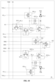
- FIG. 1 is a schematic structural diagram of a display panel according to some embodiments of the present disclosure
- FIG. 2 is a schematic structural diagram of two subpixels in a display panel according to some embodiments of the present disclosure
- FIG. 3 is a schematic structural diagram of two subpixels in another display panel according to some embodiments of the present disclosure.
- FIG. 4 is a schematic structural diagram of another display panel according to some embodiments of the present disclosure.
- FIG. 5 is a schematic structural diagram of a plurality of subpixels in a display panel according to some embodiments of the present disclosure
- FIG. 6 is a schematic structural diagram of still another display panel according to some embodiments of the present disclosure.
- FIG. 7 is a schematic structural diagram of two subpixels in still another display panel according to some embodiments of the present disclosure.
- FIG. 8 is a schematic structural diagram of two subpixels in yet another display panel according to some embodiments of the present disclosure.
- FIG. 9 is a schematic structural diagram of two subpixels in yet another display panel according to some embodiments of the present disclosure.
- FIG. 10 is a schematic structural diagram of two subpixels in yet another display panel according to some embodiments of the present disclosure.
- FIG. 11 is a schematic structural diagram of a plurality of subpixels in another display panel according to some embodiments of the present disclosure.
- FIG. 12 is a schematic structural diagram of a plurality of subpixels in still another display panel according to some embodiments of the present disclosure.
- FIG. 13 is a diagram of a partial structural layout of a display panel according to some embodiments of the present disclosure.
- FIG. 14 is a diagram of a partial structural layout of another display panel according to some embodiments of the present disclosure.
- FIG. 15 is a partial enlarged schematic diagram of the structural layout shown in FIG. 14 ;
- FIG. 16 is a diagram of a partial structural layout of still another display panel according to some embodiments of the present disclosure.
- FIG. 17 is a partial enlarged schematic diagram of the structural layout shown in FIG. 15 ;
- FIG. 18 is a diagram of a structural layout of some film layers in a display panel according to some embodiments of the present disclosure.
- FIG. 19 is a diagram of a structural layout of some film layers in another display panel according to some embodiments of the present disclosure.
- FIG. 20 is a diagram of a structural layout of some film layers in still another display panel according to some embodiments of the present disclosure.
- FIG. 21 is a diagram of a structural layout of some film layers in yet another display panel according to some embodiments of the present disclosure.
- FIG. 22 is a diagram of a structural layout of some film layers in yet another display panel according to some embodiments of the present disclosure.
- FIG. 23 is a diagram of a structural layout of some film layers in yet another display panel according to some embodiments of the present disclosure.
- FIG. 24 is a diagram of a structural layout of some film layers in yet another display panel according to some embodiments of the present disclosure.
- FIG. 25 is a diagram of a structural layout of some film layers in yet another display panel according to some embodiments of the present disclosure.
- FIG. 26 is a diagram of a structural layout of some film layers in yet another display panel according to some embodiments of the present disclosure.
- FIG. 27 is a diagram of a structural layout of some film layers in yet another display panel according to some embodiments of the present disclosure.
- FIG. 28 is a diagram of a structural layout of some film layers in yet another display panel according to some embodiments of the present disclosure.
- FIG. 29 is a sectional view of the structure shown in FIG. 14 in a kk′ direction;
- FIG. 30 is a time sequence diagram of signal lines to which subpixels in a display panel are coupled according to some embodiments of the present disclosure
- FIG. 31 is a schematic structural diagram of yet another display panel according to some embodiments of the present disclosure.
- FIG. 32 is a schematic structural diagram of a display apparatus according to some embodiments of the present disclosure.
- an OLED display panel generally includes a substrate and a plurality of subpixels on a side of the substrate.
- Each subpixel includes a pixel circuit and a light-emitting element.
- the pixel circuit is coupled to a plurality of signal lines and the light-emitting element, and is configured to drive the light-emitting element to emit light based on signals provided by the plurality of signal lines.
- Transistors used in all embodiments of the present disclosure are thin film transistors, field effect transistors, or other devices having the same characteristics.
- the transistors in the embodiments of the present disclosure are mainly switching transistors based on their functions in circuits. Because a source and drain of the switching transistor are symmetrical, the source and drain are interchangeable.
- the source is referred to as a first electrode and the drain is referred to as a second electrode, or the drain is referred to as the first electrode and the source is referred to as the second electrode.
- a middle terminal of the transistor is a gate, a signal input terminal is the source, and a signal output terminal is the drain.
- the switching transistors in the embodiments of the present disclosure include any one of an N-type switching transistor and a P-type switching transistor.
- the N-type switching transistor is turned on when the gate is at a high level and turned off when the gate is at a low level.
- the P-type switching transistor is turned on when the gate is at the low level and turned off when the gate is at the high level.
- a plurality of signals each have a first potential and a second potential. The first potential and the second potential only represent that the potential of the signal has two state quantities, but do not represent that the first potential or the second potential has a specific value in the whole text.
- e-sports display products which can better improve user experience
- the resolution is measured by the number of pixels per inch (PPI) in a display panel.
- PPI pixels per inch
- a large number of signal lines are disposed, and each subpixel (generally, a plurality of subpixels belong to one pixel) includes a large number of circuits. So, the structure is complex, which is unfavorable for the high-PPI design of the display panel.
- the embodiments of the present disclosure provide a new display panel.
- a small number of signal lines are disposed, and each subpixel includes a small number of circuits. So, the structure is simple, which facilitates the high-PPI design of the display panel and better meets user requirements.
- FIG. 1 is a schematic structural diagram of a display panel according to some embodiments of the present disclosure.
- the display panel includes a substrate 01 and a plurality of subpixels 02 arranged in an array on a side of the substrate 01 .
- the array arrangement refers to that the subpixels are sequentially arranged in a row direction and a column direction. That is, the plurality of subpixels 02 includes a plurality of rows and columns of subpixels 02 .
- At least two subpixels 02 share a first node N 1 . For example, in the display panel shown in FIG. 1 , every two adjacent subpixels 02 in the same column share the same first node N 1 .
- the display panel further includes a plurality of first control lines EM 1 and a plurality of second control lines EM 2 on the side of the substrate 01 .
- Each subpixel 02 includes a first circuit 021 and a second circuit 022 .
- the first circuit 021 is configured to control a voltage at the first node N 1 in response to a first control signal provided by the first control line EM 1 .
- the second circuit 022 is configured to control the voltage at the first node N 1 in response to a second control signal provided by the second control line EM 2 . It can be learned that in the at least two subpixels 02 sharing the first node N 1 , the first circuit 021 and the second circuit 022 jointly control the voltage at the first node N 1 .
- the first circuits 021 of the plurality of subpixels 02 are generally coupled to the plurality of first control lines EMI in a one-to-one correspondence
- the second circuits 022 are generally coupled to the plurality of second control lines EM 2 in a one-to-one correspondence. Therefore, in the display panel, the sum of the number of the plurality of first control lines EM 1 and the number of the plurality of second control lines EM 2 is twice the number of the subpixels 02 in the column direction.
- the sum of the number of the plurality of first control lines EMI and the number of the plurality of second control lines EM 2 is less than or equal to the number of the subpixels 02 in the column direction (i.e., a pixel column direction), that is, is not greater than the number of the subpixels 02 in the same column. It can be learned that in the embodiments of the present disclosure, the number of the signal lines that need to be disposed in the display panel can be reduced by sharing the node, which facilitates high-PPI design of the display panel.
- the embodiments of the present disclosure provide a display panel.
- the display panel includes a plurality of subpixels on a side of a substrate.
- Each subpixel includes a first circuit and a second circuit.
- the first circuit and the second circuit control the voltage at the first node under the control of the first control line and the second control line. Because at least two subpixels in the plurality of subpixels share the same first node, the sum of the number of the plurality of first control lines and the number of the plurality of second control lines in the display panel can be less than or equal to the number of the subpixels in the column direction. Therefore, a small number of signal lines need to be disposed in the display panel, which facilitates the high-resolution design of the display panel.
- FIG. 3 is a schematic structural diagram of another display panel according to some embodiments of the present disclosure.
- the display panel further includes a plurality of first power lines VDD and a plurality of second power lines Vinit on a side of the substrate 01 .
- Each subpixel 02 further includes a third circuit 023 and a light-emitting element L 1 .
- the first circuit 021 is coupled to the first control line EM 1 , the first power line VDD, and the first node N 1 , and is configured to control, in response to the first control signal provided by the first control line EM 1 , the first power line VDD to be connected to or disconnected from the first node N 1 .
- the first circuit 021 controls the first power line VDD to be connected to the first node N 1 when a potential of the first control signal is a first potential.
- a first power signal provided by the first power line VDD is transmitted to the first node N 1 to charge the first node N 1 .
- the first circuit 021 controls the first power line VDD to be disconnected from the first node N 1 when the potential of the first control signal is a second potential.
- the first potential is a valid potential
- the second potential is an invalid potential
- the first potential is a high potential relative to the second potential.
- the first circuit 021 is also referred to as a light emission control circuit.
- the first power line VDD is also referred to as a charging power line.
- the first power signal is also referred to as a charging power signal.
- the first control line EM 1 is also referred to as a light emission control line.
- the first control signal is also referred to as a light emission control signal.
- the second circuit 022 is coupled to the second control line EM 2 , the second power line Vinit, and the first node N 1 . That is, the second circuit 022 and the first circuit 021 are both coupled to the first node N 1 .
- the second circuit 022 is configured to control, in response to the second control signal provided by the second control line EM 2 , the second power line Vinit to be connected to or disconnected from the first node N 1 .
- the second circuit 022 controls the second power line Vinit to be connected to the first node N 1 when a potential of the second control signal is the first potential.
- a second power signal provided by the second power line Vinit is transmitted to the first node N 1 to reset the first node N 1 .
- the second circuit 022 controls the second power line Vinit to be disconnected from the first node N 1 when the potential of the second control signal is the second potential.
- the second circuit 021 is also referred to as a first reset circuit.
- the second power line Vinit is also referred to as an initial power line.
- the second power signal is also referred to as an initial power signal.
- the second control line EM 2 is also referred to as a reset control line.
- the second control signal is also referred to as a reset control signal.
- the third circuit 023 is coupled to the first node N 1 and the light-emitting element L 1 .
- the third circuit 023 is configured to drive, in response to a potential at the first node N 1 , the light-emitting element L 1 to emit light.
- the light-emitting element L 1 has a first electrode and a second electrode.
- the third circuit 023 is coupled to the first electrode of the light-emitting element L 1 .
- the second electrode of the light-emitting element L 1 is coupled to a pull-down power line VSS.
- the third circuit 023 transmits a light emission driving signal (for example, driving current) to the first electrode of the light-emitting element L 1 based on the potential at the first node N 1 .
- the light-emitting element L 1 emits light under the action of a voltage difference between the light emission driving signal and a pull-down power signal that is provided by the pull-down power line VSS and received by the second electrode.
- one of the first electrode and the second electrode of the light-emitting element L 1 is an anode, and the other is a cathode.
- the first electrode of the light-emitting element L 1 is the anode, and the second electrode is the cathode.
- the third circuit 023 is also referred to as a light emission driving circuit.
- the first circuit 021 , the second circuit 022 , and the third circuit 023 are collectively referred to as a pixel circuit.
- the at least two subpixels 02 on the basis that at least two subpixels 02 share the first node N 1 , the at least two subpixels 02 further share a target circuit and a target signal line.
- the shared target circuit includes the first circuit 021 and the second circuit 022 .
- the shared target signal line includes the first control line EM 1 and the second control line EM 2 . That is, the at least two subpixels 02 share the same first circuit 021 , the same second circuit 022 , the same first control line EM 1 , and the same second control line EM 2 .
- sharing the same circuit by the at least two subpixels 02 refers to that the at least two subpixels 02 operate under the control of the same circuit.
- the at least two subpixels 02 simultaneously perform some operations. For example, the at least two subpixels 02 sharing the first circuit 021 simultaneously charge the first nodes N 1 , and at least two subpixels 02 sharing the second circuit 022 simultaneously reset the first nodes N 1 .
- FIG. 3 shows two subpixels 02 in the same column.
- the two subpixels 02 share the same first circuit 021 and the same second circuit 022 . Therefore, the two subpixels 02 include four circuits, i.e., one first circuit 021 , one second circuit 022 , and two third circuits 023 . After the four circuits are equally divided between the two subpixels 02 , each subpixel 02 includes only two circuits. In some practices, because different subpixels 02 share no circuit, each subpixel in some practices includes three circuits on the basis of including the same types of circuits (such as the first circuit 021 , the second circuit 022 , and the third circuit 023 ).
- the number of circuits included in each of the subpixels 02 sharing the target circuit is significantly reduced, and correspondingly, the structure is simple, which further facilitates the high-PPI design of the display panel.
- the two subpixels 02 shown in FIG. 3 further share the same first control line EM 1 and the same second control line EM 2 .
- the number of the first control lines EM 1 in the display panel is 1 ⁇ 2 of the number of the subpixels in the column direction
- the number of the second control lines EM 2 is also 1 ⁇ 2 of the number of the subpixels in the column direction. Therefore, in the display panel, the sum of the number of the plurality of first control lines EM 1 and the number of the plurality of second control lines EM 2 is equal to the number of the subpixels 02 in the column direction.
- the target circuit at least includes the first circuit 021 and the second circuit 022 . That is, at least two subpixels 02 sharing the same first circuit 021 are disposed in the same column, and at least two subpixels 02 sharing the same second circuit 022 are disposed in the same column.
- the at least two subpixels 02 sharing the target circuit and disposed in the same column further share the target signal line.
- the target signal line at least includes the first control line EM 1 and the second control line EM 2 .
- the target signal line may further include the second power line Vinit.
- first control line EM 1 and the second control line EM 2 are generally coupled to a gate driver on array (GOA) circuit (also referred to as a gate drive circuit), and respectively receive a light emission control signal and a reset control signal provided by the GOA circuit. That is, the subpixel 02 operates under the drive of the GOA circuit. Therefore, the number of signal lines to which the GOA circuit is coupled decreases as the number of the first control lines EM 1 and the number of the second control lines EM 2 decrease, and thus the driving capability and operating power consumption of the GOA circuit can be reduced.
- GOA gate driver on array
- the output capability of the GOA circuit is generally positively correlated with a width-to-length ratio (reflected in an occupied area) of an output transistor included in the GOA circuit, the occupied area of the output transistor in the GOA circuit can be further reduced, which facilitates the narrow-frame design of the display panel.
- the plurality of subpixels 02 in the same column includes a plurality of subpixel groups Z 1 .
- Each subpixel group Z 1 includes two subpixels 02 in different rows, and the two subpixels 02 share a target circuit and a target signal line.
- every two subpixels 02 in the same column share the same second circuit 022 and the same third circuit 023 .
- every two subpixels 02 in the same column further share the same first control line EM 1 and the same second control line EM 2 .
- each subpixel group Z 1 includes two subpixels 02 in adjacent rows.
- the two subpixels 02 in each subpixel group Z 1 are disposed in an even row and an odd row. That is, in every two subpixels 02 sharing the target circuit and the target signal line and disposed in the same column, one subpixel 02 is disposed in an odd row, and the other subpixel 02 is disposed in an even row, and the odd row and the even row are adjacent.
- the two subpixels 02 in each subpixel group Z 1 are disposed in two adjacent rows on the basis of being disposed in the odd row and the even row. That is, for the subpixels 02 in the same column, from the subpixel 02 in the first row, the subpixels 02 in every two adjacent rows share the target circuit and the target signal line. This can facilitate layout and arrangement of the signal lines such that each signal line is short and the load on each signal line is small.
- the display panel includes M rows and N columns of subpixels 02 , wherein M and N are integers greater than 0, then for the subpixels 02 in any of the N columns, the subpixel 02 in the m th row and the subpixel 02 in the (m+1) th row share the target circuit and the target signal line, where m is an odd number and is greater than 0 and less than or equal to M.
- all subpixels 02 in the same column share the target circuit and the target signal line.
- two subpixels 02 in the same column and two non-adjacent rows share the target circuit and the target signal line.
- every three or more subpixels 02 in the same column and different rows share the target circuit and the target signal line.
- the following embodiments are illustrated by taking an example in which the subpixels 02 sharing the target circuit and the target signal line are two subpixels 02 in the same column and an odd row and an even row that are adjacent.
- the at least two subpixels 02 in the same row share the target circuit. That is, the at least two subpixels 02 sharing the same target circuit are disposed in the same row, which can simplify the structure of a large number of subpixels 02 in the display panel and further facilitate the high-PPI design of the display panel.
- the at least two subpixels 02 sharing the same target circuit are subpixels 02 in the same row only. That is, in the display panel, only at least two subpixels 02 in the same row share the target circuit.
- the at least two subpixels 02 sharing the same target circuit include subpixels 02 in the same row and subpixels 02 in the same column.
- the embodiments of the present disclosure are illustrated by taking an example in which the at least two subpixels 02 sharing the same target circuit include the subpixels 02 in the same row and the subpixels 02 in the same column.
- the display panel provided in the embodiments of the present disclosure include a plurality of pixels P 1 arranged in an array.
- Each pixel P 1 includes at least two subpixels 02 , and the at least two subpixels 02 are sequentially arranged in the row direction. That is, in the plurality of subpixels 02 in the display panel, two or more subpixels 02 arranged in the row direction constitute one pixel P 1 .
- each pixel P 1 shown in FIG. 6 includes three subpixels 02 .
- colors of the three subpixels 02 in each pixel P 1 are different.
- the colors of the three subpixels 02 in each pixel P 1 are red (R), green (G), and blue (B). That is, each pixel P 1 includes subpixels 02 of three colors, namely, R, G, and B.
- the at least two subpixels 02 sharing the target circuit and disposed in the same row belong to the same pixel P 1 . That is, for any row of subpixels 02 , at least two subpixels 02 included in each pixel P 1 share the same target circuit.
- all the subpixels 02 included in each pixel P 1 share the target circuit, which can further facilitate the high-PPI design of the display panel.
- FIG. 5 shows a total of 6 subpixels 02 in two adjacent rows and three adjacent columns.
- the 3 subpixels 02 in the same row belong to the same pixel P 1
- the 3 subpixels 02 are a red subpixel R, a green subpixel G, and a blue subpixel B, which are marked with 02 _R, 02 _G, and 02 _B in the figure.
- FIG. 5 actually shows two pixels P 1 in the same column and two adjacent rows (an odd row and an even row).
- the 3 subpixels 02 share the same second circuit 022 and the same first circuit 021 . It can be seen from FIG. 5 that the two subpixels 02 in the same column and different rows further share the same second circuit 022 and the same first circuit 021 , and correspondingly, further share the same first control line EM 1 and the same second control line EM 2 .
- each subpixel 02 in two adjacent rows and different columns include 8 circuits in total, and after the 8 circuits are equally divided among the 6 subpixels 02 , each subpixel 02 includes only 1.3 circuits. The number is significantly reduced in comparison with some practices in which each subpixel 02 includes 3 circuits. On this basis, it may be considered that in the display panel, in two pixels P 1 in the same column and an odd row and an even row, three RGB subpixels included in one pixel P 1 and three RGB subpixels included in the other pixel P 1 share the target circuit and the target signal line.
- each pixel P 1 alternatively includes 2, 4, or other number of subpixels 02 , and each pixel P 1 further includes a white (W) subpixel or a subpixel 02 of another color, which is not limited in the embodiments of the present disclosure.
- the at least two subpixels 02 sharing the target circuit and disposed in the same row alternatively belong to different pixels P 1 .
- the at least two subpixels 02 sharing the same target circuit belong to different pixels P 1
- at least one subpixel 02 in each pixel P 1 and at least one subpixel 02 in another pixel P 1 share the same target circuit.
- FIG. 7 is a schematic structural diagram of another display panel according to some embodiments of the present disclosure.
- the display panel further includes a plurality of third control lines G 1 , a plurality of fourth control lines G 2 , and a plurality of data lines D 1 on a side of the substrate 01 .
- the third circuit 023 includes a first sub-circuit 0231 , a second sub-circuit 0232 , a third sub-circuit 0233 , and a fourth sub-circuit 0234 .
- the first sub-circuit 0231 is coupled to the third control line G 1 , the data line D 1 , and a second node N 2 .
- the first sub-circuit 0231 is configured to control, in response to a third control signal provided by the third control line G 1 , the data line D 1 to be connected to or disconnected from the second node N 2 .
- the first sub-circuit 0231 controls the data line D 1 to be connected to the second node N 2 when a potential of the third control signal is the first potential.
- a data signal provided by the data line D 1 is transmitted to the second node N 2 .
- the first sub-circuit 0231 controls the data line D 1 to be disconnected from the second node N 2 when the potential of the third control signal is the second potential.
- the first sub-circuit 0231 is also referred to as a data writing sub-circuit, and the third control line G 1 is also referred to as a first gate line.
- the third control signal is also referred to as a first gate driving signal.
- the second sub-circuit 0232 is coupled to the fourth control line G 2 , the second node N 2 , and a third node N 3 .
- the second sub-circuit 0232 is configured to control, in response to a fourth control signal provided by the fourth control line G 2 , the second node N 2 to be connected to or disconnected from the third node N 3 .
- the second sub-circuit 0232 controls the second node N 2 to be connected to the third node N 3 when a potential of the fourth control signal is the first potential.
- the signal (for example, data signal) transmitted to the second node N 2 is further transmitted to the third node N 3 .
- the second sub-circuit 0232 controls the second node N 2 to be disconnected from the third node N 3 when the potential of the fourth control signal is the second potential.
- the second sub-circuit 0232 is also referred to as a second data writing sub-circuit, and the fourth control line G 4 is also referred to as a second gate line.
- the fourth control signal is also referred to as a second gate driving signal.
- the third sub-circuit 0233 is coupled to the third node N 3 and the light-emitting element L 1 .
- the third sub-circuit 0233 is configured to adjust the potential at the third node N 3 and the potential of the light-emitting element L 1 .
- the third sub-circuit 0233 adjusts the potential at the third node N 3 and the potential of the light-emitting element L 1 through a coupling effect.
- the third sub-circuit 0233 is referred to as an adjustment sub-circuit.
- the fourth sub-circuit 0234 is coupled to the third node N 3 , the first node N 1 , and the light-emitting element L 1 .
- the fourth sub-circuit 0234 is configured to transmit a light emission driving signal (for example, driving current) to the light-emitting element L 1 based on the potential at the first node N 1 and the potential at the third node N 3 to drive the light-emitting element L 1 to emit light.
- the fourth sub-circuit 0234 is also referred to as a drive sub-circuit.
- the shared target circuit described in the embodiments of the present disclosure further includes the first sub-circuit 0231 .
- the at least two subpixels 02 in the same column share the same first sub-circuit 0231 .
- the at least two subpixels 02 in the same column further share the same second node N 2 and the same third control line G 1 .
- the target signal line further includes the third control line G 1 . This can further simplify the circuit structure of the subpixel 02 and reduce the number of signal lines that need to be disposed.
- FIG. 7 shows two subpixels 02 (marked with 02 _e and 02 _o) in the same column and an odd row and an even row.
- the two subpixels 02 _e and 02 _o not only share the same second circuit 022 and the same first circuit 021 , but also share the same first sub-circuit 0231 .
- the two subpixels 02 _e and 02 _o share the same first control line EM 1 , the same second control line EM 2 , and the same third control line G 1 .
- the least two subpixels 02 in the same column are configured to share the first sub-circuit 0231 such that a data signal provided by one data line D 1 can be simultaneously transmitted to the second nodes N 2 of the subpixels 02 . Then, when the fourth control line G 2 to which each subpixel 02 is coupled provides the fourth control signal at the first potential, each subpixel 02 further transmits the data signal received by the second node N 2 thereof to the third node N 3 thereof.
- the third control signal provided by the third control line G 1 can be flexibly controlled such that the data signal provided by the same data line D 1 is transmitted to different subpixels 02 in the same column in a time-sharing manner.
- every two subpixels 02 regarded as one subpixel group Z 1
- every two subpixel groups Z 1 include different first sub-circuits 0231 .
- the third control signals provided by the third control lines G 1 to which the first sub-circuits 0231 are coupled can be flexibly controlled such that the same data line D 1 is connected to the second nodes N 2 of the subpixel groups Z 1 simultaneously or in a time-sharing manner.
- the third control line G 1 is considered as a column-direction partition control switch, and is configured to control a partition to emit light only without data refreshing in one frame of scanning such that data bandwidth of the data line D 1 is not occupied, thereby providing a high-frequency refreshing drive function for a high-resolution partition (a region obtained through manual division).
- FIG. 8 is a schematic structural diagram of yet another display panel according to some embodiments of the present disclosure. As shown in FIG. 8 , the display panel further includes a plurality of fifth control lines G 3 and a plurality of third power lines Vref on a side of the substrate 01 , and each subpixel 02 further includes a fourth circuit 024 .
- the fourth circuit 024 is coupled to the fifth control line G 3 , the third power line Vref, and the third node N 3 .
- the fourth circuit 024 is configured to control, in response to a fifth control signal provided by the fifth control line G 3 , the third power line Vref to be connected to or disconnected from the third node N 3 .
- the fourth circuit 024 controls the third power line Vref to be connected to the third node N 3 when a potential of the fifth control signal is the first potential.
- a third power signal provided by the third power line Vref is transmitted to the third node N 3 to reset the third node N 3 .
- the fourth circuit 024 controls the third power line Vref to be disconnected from the third node N 3 when the potential of the fifth control signal is the second potential.
- the fourth circuit 024 is also referred to as a second reset circuit, and the fifth control line G 3 is also referred to as a third gate line G 3 .
- the fifth control signal is also referred to as a third gate driving signal.
- the third power line Vref is also referred to as a reset power line.
- the third power signal is also referred to as a reset power signal.
- the at least two subpixels 02 in the same column further share the same third power line Vref. That is, the target signal line further includes the third power line Vref, which can further reduce the number of signal lines that need to be disposed in the display panel.
- FIG. 9 does not show the first circuit 021 and the second circuit 022 , and the signal lines to which these two circuits are coupled.
- FIG. 8 and FIG. 9 show a display panel based on the structure shown in FIG. 7 . That is, FIG. 8 and FIG. 9 merely schematically show the two subpixels 02 _e and 02 _o in the same column and the odd row and the even row.
- FIG. 8 because the two subpixels 02 _e and 02 _o do not share the third power line Vref, the third power line Vref to which the subpixel 02 _e in the odd row is coupled is marked with Vref_e, and the third power line Vref to which the subpixel 02 _o in the even row is coupled is marked with Vref_o.
- the two adjacent subpixels 02 in the same column share the same third power line Vref.
- FIG. 10 is a schematic structural diagram of yet another display panel.
- the first circuit 021 includes a first transistor Tem 1 (which is also referred to as a first reset transistor).
- the second circuit 022 includes a second transistor Tem 2 (which is also referred to as a light emission control transistor).
- the first sub-circuit 0231 includes a third transistor T 1 (which is also referred to as a first data writing transistor).
- the second sub-circuit 0232 includes a fourth transistor T 2 (which is also referred to as a second data writing transistor).
- the third sub-circuit 0233 includes a storage capacitor C 1 .
- the fourth sub-circuit 0234 includes a fifth transistor DT (which is also referred to as a driving transistor).
- the fourth circuit 024 includes a sixth transistor T 3 (which is also referred to as a second reset transistor).
- a gate of the first transistor Tem 1 is coupled to the first control line EM 1 , a first electrode of the first transistor Tem 1 is coupled to the first power line VDD, and a second electrode of the first transistor Tem 1 is coupled to the first node N 1 .
- a gate of the second transistor Tem 2 is coupled to the second control line EM 2 , a first electrode of the second transistor Tem 2 is coupled to the second power line Vinit, and a second electrode of the second transistor Tem 2 is coupled to the first node N 1 .
- a gate of the third transistor T 1 is coupled to the third control line G 1 , a first electrode of the third transistor T 1 is coupled to the data line D 1 , and a second electrode of the third transistor T 1 is coupled to the second node N 2 .
- a gate of the fourth transistor T 2 is coupled to the fourth control line G 2 , a first electrode of the fourth transistor T 2 is coupled to the second node N 2 , and a second electrode of the fourth transistor T 2 is coupled to the third node N 3 .
- a first terminal of the storage capacitor C 1 is coupled to the third node N 3 and a second terminal of the storage capacitor C 1 is coupled to the light-emitting element L 1 .
- a gate of the fifth transistor DT is coupled to the third node N 3 , a first electrode of the fifth transistor DT is coupled to the first node N 1 , and a second electrode of the fifth transistor DT is coupled to the light-emitting element L 1 .
- the second electrode of the fifth transistor DT is coupled to the anode of the light-emitting element L 1 , and the cathode of the light-emitting element L 1 is further coupled to the pull-down power line VSS.
- a gate of the sixth transistor T 3 is coupled to the fifth control line G 3 , a first electrode of the sixth transistor T 3 is coupled to the third power line Vref, and a second electrode of the sixth transistor T 3 is coupled to the third node N 3 .
- reference numerals of circuits, signal lines, and nodes in the subpixel 02 _e are added with “_e”
- reference numerals of circuits, signal lines, and nodes in the subpixel 02 _o added with “_o” to distinguish between the two subpixels 02 _e and 02 _o.
- the two subpixels 02 _e and 02 _o in the same column and the odd row and the even row share the same first transistor Tem 1 , the same second transistor Tem 2 , and the same third transistor T 1 , and correspondingly, share the same first control line EM 1 , the same second control line EM 2 , the same second power line Vinit, and the same third control line G 1 .
- the two subpixels 02 include 9 transistors in total. After the 9 transistors are equally divided among the two subpixels 02 , each subpixel 02 includes only 4.5 transistors. That is, the subpixel provided in the embodiments of the present disclosure has a 4.5T1C structure (including 4.5 transistors and 1 capacitor). If the transistors are not shared, each of the two subpixels 02 needs to include 6 transistors and 1 capacitor. That is, the subpixel in some practices generally has a 6T1C structure. Therefore, in the embodiments of the present disclosure, the 6T1C structure is simplified into the 4.5T1C structure to reliably facilitate the high-PPI design of the display panel.
- the transistors included in each subpixel 02 are N-type transistors, and the material of the N-type transistors includes low temperature polysilicon (LTPS). That is, the pixel circuit included in the subpixel 02 is an LTPS N-type pixel circuit.
- the transistors included in each subpixel 02 are alternatively P-type transistors; or some of the transistors are P-type transistors and the other transistors are N-type transistors.
- the material of the N-type transistors is not limited to LTPS, and may alternatively be oxide.
- the first potential is a high potential relative to the second potential.
- the P-type transistor the first potential is a low potential relative to the second potential.
- the foregoing merely schematically illustrates an optional structure of the subpixel 02 , i.e., the 4.5T1C (4.5 transistors and 1 capacitor) structure.
- the structure of the subpixel 02 is not limited in the embodiments of the present disclosure, and may alternatively be other structures.
- FIG. 11 is a schematic structural diagram of yet another display panel.
- FIG. 11 shows a total of 2 pixels P 1 in adjacent odd and even rows, and a total of 6 subpixels 02 .
- the 6 subpixels 02 share the same first transistor Tem 1 and the same second transistor Tem 2 .
- the data lines D 1 to which the 3 columns of subpixels 02 are coupled are marked with D 1 - 1 , D 1 - 2 , and D 1 - 3 to distinguish between the data lines D 1 .
- FIG. 12 is a schematic structural diagram of yet another display panel.
- FIG. 12 shows a total of 4 pixels P 1 in adjacent odd and even rows, and a total of 12 subpixels.
- the 6 subpixels 02 included in every 2 pixels P 1 in the same column and adjacent rows share the same first transistor Tem 1 and the same second transistor Tem 2 .
- the data lines D 1 to which the 6 columns of subpixels 02 are coupled are marked with D 1 - 1 , D 1 - 2 , D 1 - 3 , D 1 - 4 , D 1 - 5 , and D 1 - 6 to distinguish between the data lines D 1 .
- FIG. 13 is an enlarged view of a partial structure of a display panel on the basis of sharing the third power line Vref.
- the third power line Vref extends in a first direction X 1 .
- the fourth control lines G 2 and the fifth control lines G 3 to which two subpixels 02 disposed in two adjacent rows and sharing the third power line Vref are coupled all extend in the first direction X 1 , are sequentially arranged close to the third power line Vref in a second direction X 2 , and are respectively distributed on two sides of the third power line Vref.
- the second sub-circuits 0232 included in the two subpixels 02 in two adjacent rows are distributed on two sides of the third power line Vref.
- the fourth circuits 024 included in the two subpixels 02 in two adjacent rows are distributed on two sides of the third power line Vref.
- the second sub-circuit 0232 and the fourth circuit 024 are sequentially arranged in a direction close to the third power line Vref.
- the first direction X 1 intersects the second direction X 2 , that is, the first direction X 1 is not parallel to the second direction X 2 .
- the first direction X 1 is perpendicular to the second direction X 2 .
- the first direction X 1 is the subpixel row direction
- the second direction X 2 is the subpixel column direction.
- the arrangement design shown in FIG. 13 also facilitates the layout and signal routing such that the signal lines can be arranged in a concentrated manner to further optimize the space.
- the third power line Vref is not shared is used.
- FIG. 14 shows a structural layout of another display panel by taking the structures shown in FIG. 10 and FIG. 11 as an example.
- FIG. 15 is a partial enlarged view of FIG. 14 .
- the second control line EM 2 , the second power line Vinit, and the first control line EM 1 all extend in the first direction X 1 and are sequentially arranged in the second direction X 2 .
- the first control line EM 1 and the second control line EM 2 are distributed on different sides of the second power line Vinit.
- the second control line EM 2 and the first control line EM 1 are not equidistant from the second power line Vinit in the second direction X 2 .
- a and B being arranged or distributed on different sides (i.e., two sides) of C refers to that A and B are disposed on different sides of C on the substrate 01 , for example, upper and lower sides shown in the figure.
- a and B being arranged on two sides of C alternatively refers to that A and B are symmetrically arranged on two sides of C.
- the symmetrical arrangement may be understood as that A and B overlap with each other after being folded with C as an axis of symmetry.
- A, B, and C are merely used to represent different structures, but are not identifiers of specific structures.
- the second control line EM 2 and the first control line EM 1 are arranged on two sides of the second power line Vinit
- A is used to represent the second control line EM 2
- B is used to represent the first control line EM 1
- C is used to represent the second power line Vinit.
- the second control line EM 2 and the first control line EM 1 being distributed on two sides of the second power line Vinit refers to that the second control line EM 2 and the first control line EM 1 are disposed on upper and lower sides of the second power line Vinit on the substrate 01 .
- two subpixels 02 disposed in two adjacent rows and sharing the first circuit 021 , the second circuit 022 , the first sub-circuit 0231 , the first control line EM 1 , the second control line EM 2 , and the third control line G 1 are arranged on two sides of the second power line Vinit.
- the third power lines Vref, the fifth control lines G 3 , and the fourth control lines G 2 to which the two subpixels 02 in the two adjacent rows are coupled all extend in the first direction X 1 , are sequentially arranged close to the second power line Vinit in the second direction X 2 , and are respectively arranged on the two sides of the second power line Vinit.
- the third control lines G 1 to which the two subpixels 02 in the two adjacent rows are coupled each include a first portion G 11 and a second portion G 12
- the first power line VDD includes a first portion VDD- 1 and a second portion VDD- 2
- the first portion G 11 of the third control line G 1 and the first portion VDD- 1 of the first power line VDD are sequentially arranged in the first direction X 1 and extend in the second direction X 2
- the second portion G 12 of the third control line G 1 and the second portion VDD- 2 of the first power line VDD are sequentially arranged in the second direction X 2 and extend in the first direction X 1 .
- the second portion G 12 of the third control line G 1 is disposed on the side of the second control line EM 2 away from the second power line Vinit, and the second portion VDD- 2 of the first power line VDD is disposed on the side of the first control line EM 1 away from the second power line Vinit.
- the data lines D 1 to which the two subpixels 02 in the two adjacent rows are coupled extend in the second direction X 2 , are sequentially arranged in the first direction X 1 , and are disposed between the first portion G 11 of the third control line G 1 and the first portion VDD- 1 of the first power line VDD.
- the second transistor Tem 2 shared by the two subpixels 02 is generally coupled to the second power line Vinit through a via hole.
- distances L 0 from the via hole through which the second transistor Tem 2 is coupled to the second power line Vinit to the two subpixels 02 are generally not equal.
- FIG. 16 shows a structural layout of another display panel by taking the structures shown in FIG. 10 and FIG. 11 as an example.
- FIG. 17 is a partial enlarged view of FIG. 16 .
- the second power line Vinit, the second control line EM 2 , and the first control line EM 1 all extend in the first direction X 1 , and are sequentially arranged in the second direction X 2 .
- the first control line EM 1 and the second control line EM 2 are disposed on the same side of the second power line Vinit, and the first control line EM 1 and the second power line Vinit are not equidistant from the second control line EM 2 in the second direction X 2 .
- the second power line Vinit and the first control line EM 1 are distributed on two sides (for example, upper and lower sides in the figure) of the second control line EM 2 .
- two subpixels 02 disposed in two adjacent rows and sharing the first circuit 021 , the second circuit 022 , the first sub-circuit 0231 , the first control line EM 1 , the second control line EM 2 , and the third control line G 1 are arranged on two sides of the second control line EM 2 .
- the third power lines Vref, the fifth control lines G 3 , and the fourth control lines G 2 to which the two subpixels 02 in the two adjacent rows are coupled all extend in the first direction X 1 , are sequentially arranged close to the second control line EM 2 in the second direction X 2 , and are respectively arranged on two sides of the second control line EM 2 .
- the third control lines G 1 to which the two subpixels 02 in the two adjacent rows are coupled each include a first portion G 11 and a second portion G 12
- the first power line VDD includes a first portion VDD- 1 and a second portion VDD- 2
- the first portion G 11 of the third control line G 1 and the first portion VDD- 1 of the first power line VDD are sequentially arranged in the first direction X 1 and extend in the second direction X 2
- the second portion G 12 of the third control line G 1 and the second portion VDD- 2 of the first power line VDD are sequentially arranged in the second direction X 2 and extend in the first direction X 1 .
- the second portion G 12 of the third control line G 1 is disposed on the side of the second power line Vinit away from the second control line EM 2
- the second portion VDD- 2 of the first power line VDD is disposed on the side of the first control line EM 1 away from the second control line EM 2
- the data lines D 1 to which the two subpixels 02 in the two adjacent rows are coupled extend in the second direction X 2 , are sequentially arranged in the first direction X 1 , and are disposed between the first portion G 11 of the third control line G 1 and the first portion VDD- 1 of the first power line VDD.
- the distances L 0 from the via hole through which the second transistor Tem 2 is coupled to the second power line Vinit to the two subpixels 02 are approximately equal. Being approximately equal refers to that a ratio of the distance L 0 from the via hole to one of the subpixels 02 to the distance L 0 from the via hole to the other subpixel 02 ranges from 0.9 to 1.1. In this way, signals transmitted to the two subpixels 02 are as same as possible, that is, the signals transmitted to the two subpixels 02 have good uniformity such that the display luminance of the two subpixels 02 has good uniformity and the display effect of the display panel can be improved.
- the layout and signal routing can be facilitated such that the signal lines can be arranged in a concentrated manner to further optimize the space.
- the first circuit 021 and the second circuit 022 shared by the two subpixels 02 in the two adjacent rows are sequentially arranged in a third direction X 3 (as shown in FIG. 15 ), and the first circuit 021 and the second circuit 022 are not equidistant from the same subpixel 02 in the two subpixels 02 in the two adjacent rows.
- the third direction X 3 intersects (that is, is not perpendicular to) the first direction X 1 and the second direction X 2 .
- the first circuit 021 and the second circuit 022 shared by at least two subpixels 02 in the same column are arranged at two ends of a diagonal line.
- the first circuit 021 and the second circuit 022 are disposed opposite to each other at two ends of a diagonal line Ln extending in the third direction X 3 , which can also facilitate the layout and signal routing, and further optimize the space.
- first circuit 021 and the second circuit 022 are not limited to being arranged at the two ends of the diagonal line as mentioned in the foregoing embodiments, that is, may be flexibly set as required.
- the first circuit 021 and the second circuit 022 are sequentially arranged in the row direction, that is, disposed in the same row.
- the first circuit 021 and the second circuit 022 are sequentially arranged in the column direction, that is, disposed in the same column.
- the positions of the first circuit 021 and the second circuit 022 relative to the subpixel 02 may be flexibly adjusted based on actual conditions, and may be close to any subpixel 02 in a pixel P 1 , which is not specifically limited in the embodiments of the present disclosure.
- FIG. 18 shows a structural layout of yet another display panel.
- FIG. 19 shows a structural layout of yet another display panel.
- the display panel provided in the embodiments of the present disclosure further includes an active layer Poly disposed between the substrate 01 and the light-emitting element 01 .
- the active layer Poly includes active regions p 1 of the transistors in the subpixels.
- the active layer Poly of the subpixel 02 includes a first portion Po 1 and a second portion Po 2 arranged at intervals in the second direction X 2 .
- the first portion Po 1 includes an active region T 3 -p 1 of the sixth transistor T 3 and an active region T 2 -p 1 of the fourth transistor T 2 in the subpixel 02 .
- the second portion Po 2 includes an active region DT-p 1 of the fifth transistor DT.
- the first portion Po 1 of the active layer Poly of one subpixel 02 further includes an active region T 1 -p 1 of the shared third transistor T 1 .
- the active layer Poly of the two subpixels 02 in the two adjacent rows further includes a third portion Po 3 and a fourth portion Po 4 that are arranged at intervals in the first direction X 1 and are shared.
- the third portion Po 3 includes an active region Tem 1 -p 1 of the shared first transistor Tem 1 .
- the fourth portion Po 4 includes an active region Tem 2 -p 1 of the shared second transistor Tem 2 .
- the third portion Po 3 and the second portion Po 2 of the active layer Poly of each subpixel 02 are integrated, that is, are integrally formed.
- the first portion Po 1 , the second portion Po 2 , the third portion Po 3 , and the fourth portion Po 4 of the active layer Poly each further includes a conducting region p 2 .
- An orthographic projection of the conducting region p 2 on the substrate 01 does not overlap an orthographic projection of the active region p 1 on the substrate 01 .
- the conducting region p 2 of the second portion Po 2 and the conducting region p 2 of the third portion Po 3 are configured to couple the two subpixels 02 in the two adjacent rows.
- the active region is also referred to as a channel region.
- the conducting region p 2 includes a source region and a drain region on two sides of the channel region.
- the channel region is undoped or doped in a different type from the source region and drain region.
- the channel region has semiconductor characteristics.
- the conducting region p 2 is doped and thus is electrically conductive. Doped impurities vary with the type of transistor (i.e., N type or P type). Coupling between the source and drain of different transistors is considered as coupling between the source region and drain region, that is coupling through the conducting region.
- the source is the first electrode
- the drain is the second electrode.
- the sum of the length of the conducting region p 2 of the second portion Po 2 and the length of the conducting region p 2 of the third portion Po 3 of the subpixel 02 is 0.8 to 1.2 times the length of the subpixel 02 , that is, the sum of the length of the conducting region p 2 of the second portion Po 2 and the length of the conducting region p 2 of the third portion Po 3 of the subpixel 02 is approximately equal to the length of the subpixel 02 , which can further facilitate the high-PPI design.
- FIG. 20 shows a structural layout of yet another display panel.
- FIG. 21 shows a structural layout of yet another display panel.
- the display panel further includes a first conductive layer GT 1 on the side of the active layer Poly away from the substrate 01 .
- the first conductive layer GT 1 includes the gates g 1 of the transistors and a first electrode plate c 11 of the storage capacitor C 1 in the subpixel.
- the first conductive layer GT 1 is also referred to as a first gate metal layer.
- the first conductive layer GT 1 of the subpixel 02 includes a first portion gt 1 , a second portion gt 2 , and a third portion gt 3 arranged at intervals in the second direction X 2 .
- the first portion gt 1 includes the gate T 3 -g 1 of the sixth transistor T 3 in the subpixel 02 .
- the second portion gt 2 includes the gate T 2 -g 1 of the fourth transistor T 2 .
- the third portion gt 3 includes a first electrode plate c 11 of the storage capacitor C 1 and the gate DT-g 1 of the fifth transistor DT in the subpixel 02 .
- the first conductive layer GT 1 of one subpixel 02 further includes a fourth portion gt 4 disposed between the second portion gt 2 and the third portion gt 3 .
- the fourth portion gt 4 includes the gate T 1 -g 1 of the shared third transistor T 1 .
- the first conductive layer GT 1 of each of the two subpixels 02 in the two adjacent rows further includes a fifth portion gt 5 and a sixth portion gt 6 that are arranged at intervals in the first direction X 1 and are shared.
- the fifth portion gt 5 includes the gate Tem 1 -g 1 of the shared first transistor Tem 1 .
- the sixth portion gt 6 includes the gate Tem 2 -g 1 of the shared second transistor Tem 2 .
- an orthographic projection of the gate of the transistor on the substrate 01 overlaps an orthographic projection of the active region of the transistor on the substrate 01 .
- overlapping refers to partial overlapping or complete overlapping, and partial overlapping is used as an example for illustration in the embodiments of the present disclosure.
- FIG. 22 shows a structural layout of yet another display panel.
- the display panel further includes a second conductive layer GT 2 on the side of the first conductive layer GT 1 away from the substrate 01 .
- the second conductive layer GT 2 is also referred to as a second gate metal layer.
- the second conductive layer GT 2 includes a second electrode plate c 12 of the storage capacitor C 1 in the subpixel.
- the second conductive layer GT 2 further includes the third power line Vref and the first portion G 11 of the third control line G 1 .
- the second electrode plates c 12 of the storage capacitors C 1 in the subpixels 02 are spaced apart from each other.
- an orthographic projection of the first electrode plate c 11 of the storage capacitor C 1 in the subpixel 02 on the substrate 01 overlaps an orthographic projection of the second electrode plate c 12 on the substrate 01 .
- An orthographic projection of the third power line Vref in the second conductive layer GT 2 on the substrate 01 overlaps an orthographic projection of the first portion Po 1 of the active layer Poly in each subpixel 02 on the substrate 01 .
- FIG. 23 shows a structural layout of yet another display panel.
- the display panel further includes a first insulating layer J 1 disposed on the side of the second conductive layer GT 2 away from the substrate 01 , and a plurality of first via holes K 1 penetrating through the first insulating layer J 1 .
- FIG. 24 shows a structural layout of yet another display panel.
- FIG. 16 shows a structural layout of yet another display panel.
- the display panel further includes a third conductive layer SD 1 disposed on the side of the first insulating layer J 1 away from the substrate 01 . That is, the display panel includes the first insulating layer J 1 and the third conductive layer SD 1 sequentially laminated on the side of the second conductive layer GT 2 away from the substrate 01 , and the plurality of first via holes K 1 penetrating through the first insulating layer J 1 .
- the third conductive layer SD 1 is also referred to as a first source-drain metal layer.
- the third conductive layer SD 1 includes the first control line EM 1 , the second control line EM 2 , the second portion G 12 of the third control line G 1 , the fourth control line G 2 , the fifth control line G 3 , the second power line Vinit, the second portion VDD- 2 of the first power line VDD, and a plurality of first connection portions B 1 and a plurality of second connection portions B 2 in one-to-one correspondence with the plurality of subpixels 02 .
- the plurality of first connection portions B 1 and the plurality of second connection portions B 2 are spaced apart from each other in both the first direction X 1 and the second direction X 2 . As shown in the figure, the first connection portion B 1 and the second connection portion B 2 are both L-shaped.
- first connection portion B 1 is coupled to the second portion Po 2 of the active layer Poly of the subpixel 02 through the first via hole K 1 and the other end is coupled to the light-emitting element L 1 of the subpixel 02 , to couple the second electrode of the fifth transistor DT, the first electrode of the light-emitting element L 1 , and the second electrode plate c 12 of the storage capacitor C 1 to each other.
- the second connection portion B 2 is coupled to the first portion Po 1 of the active layer Poly of the subpixel 02 through the first via hole K 1 , to couple the first electrode plate c 11 of the storage capacitor C 1 , the second electrode of the fourth transistor T 2 , and the second electrode of the sixth transistor T 3 to each other.
- the distances L 0 from the via hole through which the second transistor Tem 2 is coupled to the second power line Vinit to the two subpixels 02 in the second direction X 2 being approximately equal refers to that the distances L 0 from the first via hole k 1 through which the second transistor Tem 2 is coupled to the second power line Vinit to the two subpixels 02 are approximately equal.
- An orthographic projection of a part, serving as the third power line Vref, of the second conductive layer GT 2 on the substrate 01 overlaps an orthographic projection of the first portion Po 1 of the active layer Poly of the subpixel 02 on the substrate 01 , and this part is coupled to the first portion Po 1 through the first via hole K 1 so as to couple the first electrode of the sixth transistor T 3 and the third power line Vref to each other.
- FIG. 26 shows a structural layout of yet another display panel.
- the display panel further includes a second insulating layer J 2 disposed on the side of the third conductive layer SD 1 away from the substrate 01 , and a plurality of second via holes K 2 penetrating through the second insulating layer J 2 .
- FIG. 27 shows a structural layout of yet another display panel.
- the display panel further includes a fourth conductive layer SD 2 disposed on the side of the second insulating layer J 2 away from the substrate 01 .
- the display panel includes the second insulating layer J 2 and the fourth conductive layer SD 2 sequentially laminated on the side of the third conductive layer SD 1 away from the substrate 01 , and the plurality of second via holes K 2 penetrating through the second insulating layer J 2 .
- the fourth conductive layer SD 2 is also referred to as a second source-drain metal layer.
- the light-emitting element L 1 includes an anode layer Anode disposed on a side of the substrate 01 .
- the fourth conductive layer SD 2 includes the first portion VDD- 1 of the first power line VDD and the data line D 1 .
- the part, serving as the first portion VDD- 1 of the first power line VDD, of the fourth conductive layer SD 2 is coupled to the part, serving as the second portion VDD- 2 of the first power line VDD, of the third conductive layer SD 1 through the second via hole K 2 , so as to couple the first portion VDD- 1 and the second portion VDD- 2 as a whole to form the first power line VDD.
- the part, serving as the data line D 1 , of the fourth conductive layer SD 2 is coupled to the first portion Po 1 through the first via hole K 1 , so as to couple the first electrode of the third transistor T 1 and the data line D 1 to each other.
- the other end of the first connection portion B 1 is coupled to the anode layer Anode of the light-emitting element L 1 through the second via hole K 2 , to couple the fifth transistor DT, the second electrode plate c 12 of the storage capacitor C 1 , and the anode of the light-emitting element L 1 to each other.
- the conductive layer including the signal lines refers to that the signal lines and the conductive layer are disposed in the same layer.
- “Being disposed in the same layer” refers to that a film layer for forming specific patterns is formed through the same film forming process, and then the film layer is patterned by using the same mask through a one-time patterning process to form the layer structure.
- the one-time patterning process includes a plurality of times of exposure, development, or etching processes, and the specific patterns in the formed layer structure are continuous or discontinuous.
- the plurality of elements, components, structures, and/or portions in the “same layer” are made from the same material and are formed through the same patterning process, which can simplify the manufacturing processes, reduce the manufacturing costs and improve manufacturing efficiency.
- the signal lines and the metal layer being disposed in the same layer refers to that the metal layer is configured to form the signal lines.
- the display panel further includes a pixel defining layer PDL disposed on the side of the anode layer Anode away from the substrate 01 .
- the pixel defining layer PDL is configured to define a light-emitting region of each subpixel 02 .
- the light-emitting element L 1 is an OLED.
- FIG. 29 is a sectional view of a display panel in a kk′ direction.
- the light-emitting element L 1 includes the anode layer Anode, a light-emitting material layer EL, and a cathode layer Cathode that are sequentially laminated on a side of the substrate 01 .
- the display panel includes the active layer Poly, the first gate metal layer GT 1 , the second gate metal layer GT 2 , the first insulating layer J 1 , the first source-drain metal layer SD 1 , the second insulating layer J 2 , and the second source-drain metal layer SD 2 that are sequentially laminated between the substrate 01 and the light-emitting element L 1 , and further includes the pixel defining layer PDL disposed between the light-emitting material layers EL of the light-emitting elements L 1 in every two subpixels 02 .
- the first insulating layer J 1 is also referred to as an interlayer dielectric layer (ILD).
- the first insulating layer J 1 and the second insulating layer J 2 are both provided with via holes.
- the conductive layers disposed on adjacent two sides of the insulating layer need to be coupled, the conductive layers can be reliably lapped through the via holes in the insulating layer.
- the first source-drain metal layer SD 1 is lapped with the active layer P 1 and the first gate metal layer GT 1 through the via holes penetrating through the first insulating layer J 1 . That is, the display panel adopts a dual-gate structure, and the via holes penetrating through the insulating layer are formed at dual-gate positions, thereby further reducing the line resistance while lapping is ensured.
- the part, serving as the fourth control line G 2 , of the third conductive layer SD 1 is coupled to the gate of the fourth transistor T 2 through three first via holes K 1 penetrating through the first insulating layer J 1 .
- the display panel further includes a third insulating layer J 3 disposed between the anode layer Anode and the fourth conductive layer SD 2 .
- a third insulating layer J 3 disposed between the anode layer Anode and the fourth conductive layer SD 2 .
- the display panel further includes a buffer layer B 1 disposed between the substrate 01 and the active layer Poly, a first gate insulating layer GI 1 disposed between the active layer Poly and the first gate metal layer GT 1 , a second gate insulating layer GI 2 disposed between the first gate metal layer GT 1 and the second gate metal layer GT 2 , and a first passivation layer PVX 1 and a second passivation layer PVX 2 sequentially laminated between the second insulating layer J 2 and the third insulating layer J 3 .
- Each film layer mentioned herein is configured to insulate two layers on different sides thereof to avoid signal interference.
- the material of the active layer P 1 includes polysilicon.
- the material of the active layer P 1 of an LTPS transistor is LTPS.
- the material of the second insulating layer J 2 and the material of the third insulating layer J 3 are an organic insulating material (for example, resin).
- the material of the anode layer Anode of the light-emitting element L 1 is indium tin oxide (ITO).
- the material of the first passivation layer PVX 1 and the material of the second passivation layer PVX 2 are an inorganic insulating material.
- the structure shown in FIG. 10 includes 4 adjacent rows of subpixels 02 (subpixels 02 belonging to one partition), the subpixel 02 in the first row, which is an odd row, and the subpixel 02 in the second row, which is an even row, share the target circuit and the target signal line, the subpixel 02 in the third row, which is an odd row, and the subpixel 02 in the fourth row, which is an even row, share the target circuit and the target signal line, and the transistor is an N-type transistor.
- the first potential is a high potential
- the second potential is a low potential.
- FIG. 30 is a time sequence diagram of signal lines to which the 4 rows of subpixels are coupled.
- the first control line EM 1 shared by the subpixel 02 in the first row and the subpixel 02 in the second row is denoted as EM 1 _ 1 .
- the first control line EM 1 shared by the subpixel 02 in the third row and the subpixel 02 in the fourth row is denoted as EM 1 _ 2 .
- the second control line EM 2 shared by the subpixel 02 in the first row and the subpixel 02 in the second row is denoted as EM 2 _ 1 .
- the second control line EM 2 shared by the subpixel 02 in the third row and the subpixel 02 in the fourth row is denoted as EM 2 _ 2 .
- the fourth control line G 2 to which the subpixel 02 in the first row is coupled is denoted as G 2 _e_ 1 .
- the fifth control line G 3 to which the subpixel 02 in the first row is coupled is denoted by G 3 _e_ 1 .
- the fourth control line G 2 to which the subpixel 02 in the second row is coupled is denoted as G 2 _o_ 1 .
- the fifth control line G 3 to which the subpixel 02 in the second row is coupled is denoted as G 3 _o_ 1 .
- the fourth control line G 2 to which the subpixel 02 in the third row is coupled is denoted as G 2 _e_ 2 .
- the fifth control line G 3 to which the subpixel 02 in the third row is coupled is denoted as G 3 _e_ 2 .
- the fourth control line G 2 to which the subpixel 02 in the fourth row is coupled is denoted as G 2 _ 0 _ 2 .
- the fifth control line G 3 to which the subpixel 02 in the fourth row is coupled is denoted as G 3 _o_ 2 .
- the third control line G 1 shared by the subpixel 02 in the first row and the subpixel 02 in the second row and the third control line G 1 shared by the subpixel 02 in the third row and the subpixel 02 in the fourth row provide third control signals at the high potential, and data is refreshed in a current frame.
- the third control lines G 1 provide the third control signals at the low potential, the display is maintained in a scanning state of a previous frame, and the data is not refreshed.
- the entire process is divided into four phases, i.e., a reset phase t 1 , a compensation phase t 2 , a data writing phase t 3 , and a light-emitting phase t 4 .
- the first control signals provided by the first control lines EM 1 _ 1 and EM 1 _ 2 are both at the low potential.
- the second control signals provided by the second control lines EM 2 _ 1 and EM 2 _ 2 are both at the high potential.
- the fourth control signals provided by the fourth control lines G 2 _o_ 1 , G 2 _e_ 1 , G 2 _o_ 2 , and G 2 _e_ 2 are all at the low potential.
- the fifth control signals provided by the fifth control lines G 3 _o_ 1 , G 3 _e_ 1 , G 3 _o_ 2 , and G 3 _e_ 2 are all at the high potential.
- the first transistor Tem 1 and the fourth transistor T 2 are both turned off, and the second transistor Tem 2 and the sixth transistor T 3 are both turned on.
- the second power signal provided by the second power line Vinit is transmitted to the first node N 1 through the turned-on second transistor Tem 2 , to simultaneously reset the first node N 1 (i.e., the source of the fifth transistor DT).
- the third power signal provided by the third power line Vref is transmitted to the third node N 3 through the turned-on sixth transistor T 3 , to simultaneously reset the third node N 3 (i.e., the gate of the fifth transistor DT).
- the third power signal transmitted to the third node N 3 is transmitted to the anode of the light-emitting element L 1 to simultaneously reset the anode of the light-emitting element L 1 (which is also considered as the drain of the fifth transistor DT) indirectly.
- the subpixels 02 in the 4 rows are simultaneously reset.
- the first control signals provided by the first control lines EM 1 _ 1 and EM 1 _ 2 are both at the high potential.
- the second control signals provided by the second control lines EM 2 _ 1 and EM 2 _ 2 are both at the low potential.
- the fourth control signals provided by the fourth control lines G 2 _o_ 1 , G 2 _e_ 1 , G 2 _o_ 2 , and G 2 _e_ 2 are all at the low potential.
- the fifth control signals provided by the fifth control lines G 3 _o_ 1 , G 3 _e_ 1 , G 3 _o_ 2 , and G 3 _e_ 2 are all at the high potential.
- the second transistor Tem 2 and the fourth transistor T 2 are both turned off, and the first transistor Tem 1 and the sixth transistor T 3 are both turned on.
- the third power line Vref continuously transmits the third power signal to the third node N 3 .
- the first power signal provided by the first power line VDD is transmitted to the first node N 1 through the turned-on first transistor Tem 1 , to simultaneously charge the first node N 1 until the potential of the signal at the source of the fifth transistor DT becomes Vref-Vth, and the compensation phase ends.
- Vth is a threshold voltage of the fifth transistor DT.
- the first control signals provided by the first control lines EM 1 _ 1 and EM 1 _ 2 are both at the low potential.
- the second control signals provided by the second control lines EM 2 _ 1 and EM 2 _ 2 are both at the low potential.
- the potentials of the fourth control signals provided by the fourth control lines G 2 _o_ 1 , G 2 _e_ 1 , G 2 _o_ 2 , and G 2 _e_ 2 sequentially become the high potential.
- the fifth control signals provided by the fifth control lines G 3 _o_ 1 , G 3 _e_ 1 , G 3 _o_ 2 , and G 3 _e_ 2 are all at the low potential.
- the first transistor Tem 1 , the second transistor Tem 2 , and the sixth transistor T 3 are all turned off.
- the fourth transistors T 2 in the subpixels 02 are sequentially turned on.
- the data signal written into the second node N 2 is transmitted to the third nodes N 3 row by row through the fourth transistors T 2 that are sequentially turned on, to sequentially charge the third nodes N 3 .
- the potential at the third node N 3 is considered as the high potential.
- the first control signals provided by the first control lines EM 1 _ 1 and EM 1 _ 2 are both at the high potential.
- the second control signals provided by the second control lines EM 2 _ 1 and EM 2 _ 2 are both at the low potential.
- the fourth control signals provided by the fourth control lines G 2 _o_ 1 , G 2 _e_ 1 , G 2 _o_ 2 , and G 2 _e_ 2 are all at the low potential.
- the fifth control signals provided by the fifth control lines G 3 _o_ 1 , G 3 _e_ 1 , G 3 _o_ 2 , and G 3 _e_ 2 are all at the low potential.
- the potential of the third node N 3 maintains the high potential in the data writing phase t 3 . Therefore, in each subpixel 02 , the second transistor Tem 2 , the fourth transistor T 2 , and the sixth transistor T 3 are all turned off, and the first transistor Tem 1 and the fifth transistor DT are turned on. Correspondingly, in each subpixel 02 , a loop is formed between the first power line VDD and the pull-down power line VSS, and the fifth transistor DT transmits a driving current to the anode of the light-emitting element L 1 based on the potential at the third node N 3 and the potential at the first node N 1 , to drive the light-emitting element L 1 to emit light. Thus, the subpixels 02 in the 4 rows simultaneously emit light.
- the first control signals provided by the first control lines EM 1 _ 1 and EM 1 _ 2 are both at the low potential, and the subpixels 02 sequentially write the data signals.
- the subpixels 02 in the 4 rows simultaneously emit light. Therefore, during writing the data signals, after the subpixels in the odd column write the date signals, the subpixels in the odd column need to wait for the subpixels in the even column to write the data signals before emitting light. In this way, when the drain of the fifth transistor DT is decoupled from the first power line VDD, the grayscale variation of the subpixels in the odd columns is not affected. Therefore, the subpixels provided in the embodiments of the present disclosure is compatible with a data line shared circuit D-Mux.
- the display panel provided in the embodiments of the present disclosure further includes a plurality of data line leads D 0 and a data line shared circuit D-Mux disposed on a side of the substrate 01 .
- the number of the plurality of data line leads D 0 is less than the number of the plurality of data lines D 1 .
- the data line shared circuit D-Mux is coupled to the plurality of data lines D 1 , and is further coupled to a source drive circuit through the plurality of data line leads D 0 .
- the data line shared circuit D-Mux is configured to transmit a data signal transmitted by the source drive circuit to one of the data line leads D 0 to at least two of the plurality of data lines D 1 in a time-sharing manner.
- the display panel includes a display region and a non-display region.
- the data line shared circuit D-Mux is generally disposed in the non-display region.
- the data lines D 1 are disposed in the display region and the non-display region.
- the operating power consumption of the source drive circuit can be reduced and the number of pins required for the source drive circuit can be reduced, thereby further facilitating narrow-frame design of the display apparatus.
- the embodiments of the present disclosure provide a display panel.
- the display panel includes a plurality of subpixels on a side of a substrate.
- Each subpixel includes a first circuit and a second circuit.
- the first circuit and the second circuit control the voltage at the first node under the control of the first control line and the second control line. Because at least two subpixels in the plurality of subpixels share the same first node, the sum of the number of the plurality of first control lines and the number of the plurality of second control lines in the display panel can be less than or equal to the number of the subpixels in the column direction. Therefore, a small number of signal lines need to be disposed in the display panel, which facilitates the high-resolution design of the display panel.
- FIG. 32 is a schematic structural diagram of a display apparatus according to some embodiments of the present disclosure. As shown in FIG. 32 , the display apparatus includes a display drive circuit 10 and the display panel 00 shown in the foregoing figures.
- the display drive circuit 10 is coupled to the signal lines in the display panel 00 .
- the display drive circuit 10 is configured to provide signals for the signal lines.
- the display drive circuit 10 includes the GOA circuit and the source drive circuit described in the foregoing embodiments.
- the GOA circuit is coupled to the plurality of third control lines G 1 , the plurality of fourth control lines G 2 , the plurality of fifth control lines G 3 , the plurality of first control lines EM 1 , and the plurality of second control lines EM 2 in the display panel 00 , and is configured to provide third control signals for the third control lines G 1 , provide fourth control signals for the fourth control lines G 2 , provide fifth control signals for the fifth control lines G 3 , provide light emission control signals for the first control lines EM 1 , and provide reset control signals for the second control lines EM 2 .
- the source drive circuit is coupled to the plurality of data lines D 1 in the display panel and configured to provide data signals for the data lines D 1 .
- the source drive circuit is indirectly coupled to the data lines D 1 through the data line leads D 0 .
- the display apparatus is any product or component having a display function, such as an OLED apparatus, electronic paper, a mobile phone, a tablet computer, a television, a display, a notebook computer, a digital photo frame, or a navigator.
- a display function such as an OLED apparatus, electronic paper, a mobile phone, a tablet computer, a television, a display, a notebook computer, a digital photo frame, or a navigator.
- At least two means two or more. At least one of A and B includes three situations: A exists alone, B exists alone, or A and B coexist.
Landscapes
- Engineering & Computer Science (AREA)
- Physics & Mathematics (AREA)
- Computer Hardware Design (AREA)
- General Physics & Mathematics (AREA)
- Theoretical Computer Science (AREA)
- Microelectronics & Electronic Packaging (AREA)
- Devices For Indicating Variable Information By Combining Individual Elements (AREA)
- Electroluminescent Light Sources (AREA)
Abstract
Description
-
- a substrate;
- a plurality of first control lines and a plurality of second control lines on a side of the substrate; and
- a plurality of subpixels arranged in an array on the side of the substrate, wherein at least two of the plurality of subpixels share a first node.
-
- the target circuit includes the first circuit and the second circuit; and the target signal line includes the first control line and the second control line.
-
- the first circuit is coupled to the first control line, the first power line, and the first node, and is configured to control, in response to the first control signal provided by the first control line, the first power line to be connected to or disconnected from the first node; and
- the second circuit is coupled to the second control line, the second power line, and the first node, and is configured to control, in response to the second control signal provided by the second control line, the second power line to be connected to or disconnected from the first node.
-
- the first transistor includes a gate coupled to the first control line, a first electrode coupled to the first power line, and a second electrode coupled to the first node; and
- the second transistor includes a gate coupled to the second control line, a first electrode coupled to the second power line, and a second electrode coupled to the first node.
-
- the third circuit includes a first sub-circuit, a second sub-circuit, a third sub-circuit, and a fourth sub-circuit;
- the first sub-circuit is coupled to the third control line, the data line, and a second node, and is configured to control, in response to a third control signal provided by the third control line, the data line to be connected to or disconnected from the second node;
- the second sub-circuit is coupled to the fourth control line, the second node, and a third node, and is configured to control, in response to a fourth control signal provided by the fourth control line, the second node to be connected to or disconnected from the third node;
- the third sub-circuit is coupled to the third node and the light-emitting element, and is configured to adjust a potential of the third node and a potential of the light-emitting element;
- the fourth sub-circuit is coupled to the third node, the first node, and the light-emitting element, and is configured to drive, based on the potential of the first node and the potential of the third node, the light-emitting element to emit light; and
- the target circuit shared by the at least two subpixels in the same column further includes the first sub-circuit; and the target signal line shared by the at least two subpixels in the same column further includes the third control line.
-
- the third transistor includes a gate coupled to the third control line, a first electrode coupled to the data line, and a second electrode coupled to the second node;
- the fourth transistor includes a gate coupled to the fourth control line, a first electrode coupled to the second node, and a second electrode coupled to the third node;
- the storage capacitor includes a first terminal coupled to the third node and a second terminal coupled to the light-emitting element; and
- the fifth transistor includes a gate coupled to the third node, a first electrode coupled to the first node, and a second electrode coupled to the light-emitting element.
-
- the data line shared circuit is coupled to the plurality of data lines, and is further coupled to a source drive circuit through the plurality of data line leads, and the data line shared circuit is configured to transmit a data signal transmitted by the source drive circuit to one of the data line leads to at least two of the plurality of data lines in a time-sharing manner.
-
- the subpixel further includes a fourth circuit, and the fourth circuit is coupled to the fifth control line, the third power line, and the third node, and is configured to control, in response to a fifth control signal provided by the fifth control line, the third power line to be connected to or disconnected from the third node.
-
- the sixth transistor includes a gate coupled to the fifth control line, a first electrode coupled to the third power line, and a second electrode coupled to the third node.
-
- the fourth control lines and the fifth control lines to which two subpixels located in two adjacent rows and sharing the third power line in the plurality of subpixels are coupled all extend in the first direction, are sequentially arranged close to the third power line in a second direction, and are distributed on two sides of the third power line, the second sub-circuits included in the two subpixels in the two adjacent rows are distributed on the two sides of the third power line, the fourth circuits included in the two subpixels in the two adjacent rows are distributed on the two sides of the third power line, and the second sub-circuits and the fourth circuits are sequentially arranged in a direction close to the third power line; and
- the first direction intersects the second direction.
-
- two subpixels located in two adjacent rows and sharing the first circuit, the second circuit, the first sub-circuit, the first control line, the second control line, and the third control line in the plurality of subpixels are arranged on two sides of the second power line, and the third power lines, the fifth control lines, and the fourth control lines to which the two subpixels in the two adjacent rows are coupled all extend in the first direction, are sequentially arranged close to the second power line in the second direction, and are arranged on the two sides of the second power line; and
- the first direction intersects the second direction.
-
- the first portion of the third control line and the first portion of the first power line are sequentially arranged in the first direction and extend in the second direction, the second portion of the third control line and the second portion of the first power line are sequentially arranged in the second direction and extend in the first direction, the second portion of the third control line is located on a side of the second control line away from the second power line, the second portion of the first power line is located on a side of the first control line away from the second power line, the data lines to which the two subpixels in the two adjacent rows are coupled extend in the second direction, are sequentially arranged in the first direction, and are located between the first portion of the third control line and the first portion of the first power line, and the first direction intersects the second direction.
-
- two subpixels located in two adjacent rows and sharing the first circuit, the second circuit, the first sub-circuit, the first control line, the second control line, and the third control line in the plurality of subpixels are arranged on two sides of the second control line, and the third power lines, the fifth control lines, and the fourth control lines to which the two subpixels in the two adjacent rows are coupled all extend in the first direction, are sequentially arranged close to the second control line in the second direction, and are arranged on the two sides of the second control line; and
- the first direction intersects the second direction.
-
- the first portion of the third control line and the first portion of the first power line are sequentially arranged in the first direction and extend in the second direction, the second portion of the third control line and the second portion of the first power line are sequentially arranged in the second direction and extend in the first direction, the second portion of the third control line is located on a side of the second power line away from the second control line, the second portion of the first power line is located on a side of the first control line away from the second control line, the data lines to which the two subpixels in the two adjacent rows are coupled extend in the second direction, are sequentially arranged in the first direction, and are located between the first portion of the third control line and the first portion of the first power line, and the first direction intersects the second direction.
-
- the via hole through which the second transistor is coupled to the second power line is approximately equidistant from the two subpixels in the two adjacent rows in the second direction.
-
- for one subpixel, an active layer of the subpixel includes a first portion and a second portion arranged at intervals in the second direction, the first portion includes an active region of the sixth transistor and an active region of the fourth transistor in the subpixel, and the second portion includes an active region of the fifth transistor;
- in the two subpixels in the two adjacent rows, the first portion of the active layer of one subpixel further includes an active region of the shared third transistor;
- the active layer of the two subpixels in the two adjacent rows further includes a third portion and a fourth portion that are arranged at intervals in the first direction and are shared, the third portion includes an active region of the shared first transistor, the fourth portion includes an active region of the shared second transistor, and the third portion and the second portion of the active layer of each subpixel are integrated; and
- the first portion, the second portion, the third portion, and the fourth portion of the active layer each include a conducting region, an orthographic projection of the conducting region on the substrate does not overlap an orthographic projection of the active region on the substrate, and the conducting region of the second portion and the conducting region of the third portion are used to couple the two subpixels in the two adjacent rows.
-
- for one subpixel, a first conductive flayer of the subpixel includes a first portion, a second portion, and a third portion arranged at intervals in the second direction, the first portion includes the gate of the sixth transistor in the subpixel, the second portion includes the gate of the fourth transistor, the third portion includes the first plate of the storage capacitor and the gate of the fifth transistor in the subpixel;
- in the two subpixels in the two adjacent rows, the first conductive layer of one subpixel further includes a fourth portion located between the second portion and the third portion, and the fourth portion includes the gate of the shared third transistor;
- the first conductive layer of the two subpixels in the two adjacent rows further includes a fifth portion and a sixth portion that are arranged at intervals in the first direction and are shared, the fifth portion includes the gate of the shared first transistor, and the sixth portion includes the gate of the shared second transistor; and
- for each transistor, an orthographic projection of the gate of the transistor on the substrate overlaps an orthographic projection of the active region of the transistor on the substrate.
-
- the second conductive layer further includes the third power lines and the first portions of the third control lines;
- in the second conductive layer, the second plates of the storage capacitors in the subpixels are spaced from each other, and for each subpixel, an orthographic projection of the first plate of the storage capacitor in the subpixel on the substrate overlaps an orthographic projection of the second plate on the substrate; and
- an orthographic projection of the third power line in the second conductive layer on the substrate overlaps an orthographic projection of the first portion of the active layer of each subpixel on the substrate.
-
- the third conductive layer includes the first control lines, the second control lines, the second portions of the third control lines, the fourth control lines, the fifth control lines, the second power lines, the second portions of the first power lines, and a plurality of first connection portions and a plurality of second connection portions in one-to-one correspondence with the plurality of subpixels, and the plurality of first connection portions and the plurality of second connection portions are spaced apart from each other in the first direction and the second direction;
- the first connection portion corresponding to each subpixel has one end coupled to the second portion of the active layer of the subpixel through the first via hole and the other end coupled to the light-emitting element in the subpixel, to couple the second electrode of the fifth transistor, the light-emitting element, and the first plate of the storage capacitor to each other;
- the second connection portion is coupled to the first portion of the active layer of the subpixel through the first via hole, to couple the first plate of the storage capacitor, the second electrode of the fourth transistor, and the second electrode of the sixth transistor to each other;
- an orthographic projection of the first control line in the third conductive layer on the substrate overlaps an orthographic projection of the gate of the first transistor on the substrate, and the gate of the first transistor is coupled to the first control line through the first via hole;
- an orthographic projection of the second control line in the third conductive layer on the substrate overlaps an orthographic projection of the gate of the second transistor on the substrate, and the gate of the second transistor is coupled to the second control line through the first via hole;
- an orthographic projection of the second portion of the third control line in the third conductive layer on the substrate overlaps an orthographic projection of the gate of the third transistor on the substrate, and the gate of the third transistor is coupled to the third control line through the first via hole;
- an orthographic projection of the fourth control line in the third conductive layer on the substrate overlaps an orthographic projection of the gate of the fourth transistor on the substrate, and the gate of the fourth transistor is coupled to the fourth control line through the first via hole;
- an orthographic projection of the fifth control line in the third conductive layer on the substrate overlaps an orthographic projection of the gate of the sixth transistor on the substrate, and the gate of the sixth transistor is coupled to the fifth control line through the first via hole;
- an orthographic projection of the second power line in the third conductive layer on the substrate overlaps an orthographic projection of the fourth portion of the active layer of the subpixel on the substrate, and the first electrode of the second transistor is coupled to the second power line through the first via hole;
- the orthographic projection of the third power line in the second conductive layer on the substrate overlaps the orthographic projection of the first portion of the active layer of the subpixel on the substrate, and the first electrode of the sixth transistor is coupled to the third power line through the first via hole; and
- an orthographic projection of the first portion of the third control line in the second conductive layer on the substrate overlaps the orthographic projection of the second portion of the third control line in the third conductive layer on the substrate, and the first portion and the second portion of the third control line are coupled to each other through the first via hole to form the third control line.
-
- the fourth conductive layer includes the first portions of the first power lines and the data lines;
- an orthographic projection of the first portion of the first power line in the fourth conductive layer on the substrate overlaps an orthographic projection of the second portion of the first power line in the third conductive layer on the substrate, and the first portion and the second portion of the first power line are coupled to each other through the second via hole to form the first power line;
- an orthographic projection of the data line in the fourth conductive layer on the substrate overlaps an orthographic projection of the first portion of the active layer of the subpixel on the substrate, and the first electrode of the third transistor is coupled to the data line through the first via hole; and
- the other end of the first connection portion is coupled to the anode layer of the light-emitting element through the second via hole to couple the second electrode of the fifth transistor, the second plate of the storage capacitor, and the light-emitting element to each other.
-
- the third direction intersects the first direction and the second direction.
Claims (19)
Applications Claiming Priority (1)
| Application Number | Priority Date | Filing Date | Title |
|---|---|---|---|
| PCT/CN2022/098747 WO2023240465A1 (en) | 2022-06-14 | 2022-06-14 | Display panel and display device |
Publications (2)
| Publication Number | Publication Date |
|---|---|
| US20240296793A1 US20240296793A1 (en) | 2024-09-05 |
| US12300168B2 true US12300168B2 (en) | 2025-05-13 |
Family
ID=89193000
Family Applications (1)
| Application Number | Title | Priority Date | Filing Date |
|---|---|---|---|
| US18/026,827 Active US12300168B2 (en) | 2022-06-14 | 2022-06-14 | Display panel and display apparatus |
Country Status (4)
| Country | Link |
|---|---|
| US (1) | US12300168B2 (en) |
| EP (1) | EP4418250A4 (en) |
| CN (1) | CN117693786A (en) |
| WO (1) | WO2023240465A1 (en) |
Cited By (1)
| Publication number | Priority date | Publication date | Assignee | Title |
|---|---|---|---|---|
| US20260004712A1 (en) * | 2024-06-27 | 2026-01-01 | Samsung Display Co., Ltd. | Pixel, method of driving the pixel, and electronic device including the pixel |
Families Citing this family (1)
| Publication number | Priority date | Publication date | Assignee | Title |
|---|---|---|---|---|
| KR20250003141A (en) * | 2023-06-30 | 2025-01-07 | 엘지디스플레이 주식회사 | Display apparatus comprising pixel circuit |
Citations (5)
| Publication number | Priority date | Publication date | Assignee | Title |
|---|---|---|---|---|
| WO2001031624A1 (en) | 1999-10-23 | 2001-05-03 | Koninklijke Philips Electronics N.V. | Active matrix electroluminescent display device |
| US20160093250A1 (en) * | 2014-09-26 | 2016-03-31 | Au Optronics Corporation | Organic light-emitting diode pixel structure |
| US20180240407A1 (en) | 2012-12-11 | 2018-08-23 | Ignis Innovation Inc. | Pixel circuits for amoled displays |
| US20210118366A1 (en) | 2019-10-21 | 2021-04-22 | Boe Technology Group Co., Ltd. | Driving circuit, display panel, driving method and display device |
| WO2021249101A1 (en) | 2020-06-12 | 2021-12-16 | 京东方科技集团股份有限公司 | Display substrate and display apparatus |
Family Cites Families (7)
| Publication number | Priority date | Publication date | Assignee | Title |
|---|---|---|---|---|
| US9888198B2 (en) * | 2014-06-03 | 2018-02-06 | Semiconductor Components Industries, Llc | Imaging systems having image sensor pixel arrays with sub-pixel resolution capabilities |
| CN107193417B (en) * | 2017-05-24 | 2020-08-18 | 上海天马微电子有限公司 | Touch display screen and display device |
| CN109559679B (en) * | 2017-09-26 | 2024-07-09 | 京东方科技集团股份有限公司 | Touch display panel and driving method thereof, pixel circuit, and electronic device |
| TWI673695B (en) * | 2018-07-13 | 2019-10-01 | 友達光電股份有限公司 | Display panel |
| CN112117287B (en) * | 2019-06-21 | 2025-12-30 | 三星电子株式会社 | Image sensor |
| KR102933157B1 (en) * | 2020-06-30 | 2026-03-03 | 엘지디스플레이 주식회사 | Display panel and display device including the same |
| KR102740142B1 (en) * | 2020-10-21 | 2024-12-06 | 엘지디스플레이 주식회사 | Electroluminescent display device |
-
2022
- 2022-06-14 CN CN202280001740.XA patent/CN117693786A/en active Pending
- 2022-06-14 US US18/026,827 patent/US12300168B2/en active Active
- 2022-06-14 EP EP22946164.5A patent/EP4418250A4/en active Pending
- 2022-06-14 WO PCT/CN2022/098747 patent/WO2023240465A1/en not_active Ceased
Patent Citations (6)
| Publication number | Priority date | Publication date | Assignee | Title |
|---|---|---|---|---|
| WO2001031624A1 (en) | 1999-10-23 | 2001-05-03 | Koninklijke Philips Electronics N.V. | Active matrix electroluminescent display device |
| US20180240407A1 (en) | 2012-12-11 | 2018-08-23 | Ignis Innovation Inc. | Pixel circuits for amoled displays |
| US20160093250A1 (en) * | 2014-09-26 | 2016-03-31 | Au Optronics Corporation | Organic light-emitting diode pixel structure |
| US20210118366A1 (en) | 2019-10-21 | 2021-04-22 | Boe Technology Group Co., Ltd. | Driving circuit, display panel, driving method and display device |
| WO2021249101A1 (en) | 2020-06-12 | 2021-12-16 | 京东方科技集团股份有限公司 | Display substrate and display apparatus |
| US20240087516A1 (en) | 2020-06-12 | 2024-03-14 | Hefei Boe Joint Technology Co., Ltd. | Display substrate and display device |
Non-Patent Citations (1)
| Title |
|---|
| Extended European search report of counterpart European application No. 22946164.5 issued on Nov. 4, 2024, 14 pages. |
Cited By (1)
| Publication number | Priority date | Publication date | Assignee | Title |
|---|---|---|---|---|
| US20260004712A1 (en) * | 2024-06-27 | 2026-01-01 | Samsung Display Co., Ltd. | Pixel, method of driving the pixel, and electronic device including the pixel |
Also Published As
| Publication number | Publication date |
|---|---|
| US20240296793A1 (en) | 2024-09-05 |
| EP4418250A1 (en) | 2024-08-21 |
| EP4418250A4 (en) | 2024-12-04 |
| WO2023240465A1 (en) | 2023-12-21 |
| CN117693786A (en) | 2024-03-12 |
Similar Documents
| Publication | Publication Date | Title |
|---|---|---|
| US11810504B2 (en) | Display substrate and display device | |
| US11723246B2 (en) | Display panel, preparation method thereof and display device | |
| US11910678B1 (en) | Display panel and display device | |
| US20250280671A1 (en) | Display substrate | |
| US12456422B2 (en) | Display panel and display device | |
| US12376376B2 (en) | Pixel circuit with specific transistor layout and display substrate | |
| US20240365619A1 (en) | Display panel and display device | |
| US20250324850A1 (en) | Display panel and display device | |
| CN112997316A (en) | Array substrate, manufacturing and control method thereof and display device | |
| US12453256B2 (en) | Display panel and display device | |
| US12579940B2 (en) | Display substrate and display device | |
| US12300168B2 (en) | Display panel and display apparatus | |
| US20240078978A1 (en) | Display substrate, method for manufacturing the same, and display device | |
| US20240268172A1 (en) | Display substrate and display device | |
| CN114667559B (en) | Pixel circuit, display substrate and display device | |
| US20240431160A1 (en) | Display panel and display device | |
| CN117042527A (en) | Display substrate and display device | |
| CN115835730A (en) | Display substrate and display device | |
| US12563923B2 (en) | Display substrate that includes an initialization signal film layer with a plurality of portions and sub-portions, method of manufacturing the same and display device | |
| US20250081767A1 (en) | Display substrate and display device | |
| US20240138211A1 (en) | Display substrate and display device | |
| JP2025521062A (en) | Display substrate and display device | |
| CN119923678A (en) | Display substrate and display device | |
| CN121096243A (en) | Display panel and display device |
Legal Events
| Date | Code | Title | Description |
|---|---|---|---|
| AS | Assignment |
Owner name: BOE TECHNOLOGY GROUP CO., LTD., CHINA Free format text: ASSIGNMENT OF ASSIGNORS INTEREST;ASSIGNORS:YUAN, CAN;LI, YONGQIAN;YUAN, ZHIDONG;REEL/FRAME:063018/0883 Effective date: 20230206 Owner name: HEFEI BOE JOINT TECHNOLOGY CO., LTD., CHINA Free format text: ASSIGNMENT OF ASSIGNORS INTEREST;ASSIGNORS:YUAN, CAN;LI, YONGQIAN;YUAN, ZHIDONG;REEL/FRAME:063018/0883 Effective date: 20230206 |
|
| FEPP | Fee payment procedure |
Free format text: ENTITY STATUS SET TO UNDISCOUNTED (ORIGINAL EVENT CODE: BIG.); ENTITY STATUS OF PATENT OWNER: LARGE ENTITY |
|
| STPP | Information on status: patent application and granting procedure in general |
Free format text: NON FINAL ACTION MAILED |
|
| STPP | Information on status: patent application and granting procedure in general |
Free format text: RESPONSE TO NON-FINAL OFFICE ACTION ENTERED AND FORWARDED TO EXAMINER |
|
| STPP | Information on status: patent application and granting procedure in general |
Free format text: FINAL REJECTION MAILED |
|
| STPP | Information on status: patent application and granting procedure in general |
Free format text: RESPONSE AFTER FINAL ACTION FORWARDED TO EXAMINER |
|
| STPP | Information on status: patent application and granting procedure in general |
Free format text: NOTICE OF ALLOWANCE MAILED -- APPLICATION RECEIVED IN OFFICE OF PUBLICATIONS |
|
| STPP | Information on status: patent application and granting procedure in general |
Free format text: NOTICE OF ALLOWANCE MAILED -- APPLICATION RECEIVED IN OFFICE OF PUBLICATIONS |
|
| STCF | Information on status: patent grant |
Free format text: PATENTED CASE |