US12289992B2 - Display apparatus and light absorber included in display apparatus - Google Patents
Display apparatus and light absorber included in display apparatus Download PDFInfo
- Publication number
- US12289992B2 US12289992B2 US17/250,808 US201917250808A US12289992B2 US 12289992 B2 US12289992 B2 US 12289992B2 US 201917250808 A US201917250808 A US 201917250808A US 12289992 B2 US12289992 B2 US 12289992B2
- Authority
- US
- United States
- Prior art keywords
- group
- substituted
- unsubstituted
- carbon atoms
- formula
- Prior art date
- Legal status (The legal status is an assumption and is not a legal conclusion. Google has not performed a legal analysis and makes no representation as to the accuracy of the status listed.)
- Active, expires
Links
Images


Classifications
-
- C—CHEMISTRY; METALLURGY
- C07—ORGANIC CHEMISTRY
- C07D—HETEROCYCLIC COMPOUNDS
- C07D239/00—Heterocyclic compounds containing 1,3-diazine or hydrogenated 1,3-diazine rings
- C07D239/02—Heterocyclic compounds containing 1,3-diazine or hydrogenated 1,3-diazine rings not condensed with other rings
- C07D239/24—Heterocyclic compounds containing 1,3-diazine or hydrogenated 1,3-diazine rings not condensed with other rings having three or more double bonds between ring members or between ring members and non-ring members
- C07D239/28—Heterocyclic compounds containing 1,3-diazine or hydrogenated 1,3-diazine rings not condensed with other rings having three or more double bonds between ring members or between ring members and non-ring members with hetero atoms or with carbon atoms having three bonds to hetero atoms with at the most one bond to halogen, directly attached to ring carbon atoms
- C07D239/32—One oxygen, sulfur or nitrogen atom
- C07D239/34—One oxygen atom
-
- C—CHEMISTRY; METALLURGY
- C07—ORGANIC CHEMISTRY
- C07D—HETEROCYCLIC COMPOUNDS
- C07D239/00—Heterocyclic compounds containing 1,3-diazine or hydrogenated 1,3-diazine rings
- C07D239/02—Heterocyclic compounds containing 1,3-diazine or hydrogenated 1,3-diazine rings not condensed with other rings
- C07D239/24—Heterocyclic compounds containing 1,3-diazine or hydrogenated 1,3-diazine rings not condensed with other rings having three or more double bonds between ring members or between ring members and non-ring members
- C07D239/26—Heterocyclic compounds containing 1,3-diazine or hydrogenated 1,3-diazine rings not condensed with other rings having three or more double bonds between ring members or between ring members and non-ring members with only hydrogen atoms, hydrocarbon or substituted hydrocarbon radicals, directly attached to ring carbon atoms
-
- C—CHEMISTRY; METALLURGY
- C07—ORGANIC CHEMISTRY
- C07D—HETEROCYCLIC COMPOUNDS
- C07D239/00—Heterocyclic compounds containing 1,3-diazine or hydrogenated 1,3-diazine rings
- C07D239/02—Heterocyclic compounds containing 1,3-diazine or hydrogenated 1,3-diazine rings not condensed with other rings
- C07D239/24—Heterocyclic compounds containing 1,3-diazine or hydrogenated 1,3-diazine rings not condensed with other rings having three or more double bonds between ring members or between ring members and non-ring members
- C07D239/28—Heterocyclic compounds containing 1,3-diazine or hydrogenated 1,3-diazine rings not condensed with other rings having three or more double bonds between ring members or between ring members and non-ring members with hetero atoms or with carbon atoms having three bonds to hetero atoms with at the most one bond to halogen, directly attached to ring carbon atoms
- C07D239/32—One oxygen, sulfur or nitrogen atom
- C07D239/38—One sulfur atom
-
- C—CHEMISTRY; METALLURGY
- C07—ORGANIC CHEMISTRY
- C07D—HETEROCYCLIC COMPOUNDS
- C07D251/00—Heterocyclic compounds containing 1,3,5-triazine rings
- C07D251/02—Heterocyclic compounds containing 1,3,5-triazine rings not condensed with other rings
- C07D251/12—Heterocyclic compounds containing 1,3,5-triazine rings not condensed with other rings having three double bonds between ring members or between ring members and non-ring members
- C07D251/14—Heterocyclic compounds containing 1,3,5-triazine rings not condensed with other rings having three double bonds between ring members or between ring members and non-ring members with hydrogen or carbon atoms directly attached to at least one ring carbon atom
- C07D251/22—Heterocyclic compounds containing 1,3,5-triazine rings not condensed with other rings having three double bonds between ring members or between ring members and non-ring members with hydrogen or carbon atoms directly attached to at least one ring carbon atom to two ring carbon atoms
-
- C—CHEMISTRY; METALLURGY
- C07—ORGANIC CHEMISTRY
- C07D—HETEROCYCLIC COMPOUNDS
- C07D403/00—Heterocyclic compounds containing two or more hetero rings, having nitrogen atoms as the only ring hetero atoms, not provided for by group C07D401/00
- C07D403/02—Heterocyclic compounds containing two or more hetero rings, having nitrogen atoms as the only ring hetero atoms, not provided for by group C07D401/00 containing two hetero rings
- C07D403/04—Heterocyclic compounds containing two or more hetero rings, having nitrogen atoms as the only ring hetero atoms, not provided for by group C07D401/00 containing two hetero rings directly linked by a ring-member-to-ring-member bond
-
- C—CHEMISTRY; METALLURGY
- C07—ORGANIC CHEMISTRY
- C07D—HETEROCYCLIC COMPOUNDS
- C07D405/00—Heterocyclic compounds containing both one or more hetero rings having oxygen atoms as the only ring hetero atoms, and one or more rings having nitrogen as the only ring hetero atom
- C07D405/02—Heterocyclic compounds containing both one or more hetero rings having oxygen atoms as the only ring hetero atoms, and one or more rings having nitrogen as the only ring hetero atom containing two hetero rings
- C07D405/04—Heterocyclic compounds containing both one or more hetero rings having oxygen atoms as the only ring hetero atoms, and one or more rings having nitrogen as the only ring hetero atom containing two hetero rings directly linked by a ring-member-to-ring-member bond
-
- C—CHEMISTRY; METALLURGY
- C07—ORGANIC CHEMISTRY
- C07D—HETEROCYCLIC COMPOUNDS
- C07D405/00—Heterocyclic compounds containing both one or more hetero rings having oxygen atoms as the only ring hetero atoms, and one or more rings having nitrogen as the only ring hetero atom
- C07D405/02—Heterocyclic compounds containing both one or more hetero rings having oxygen atoms as the only ring hetero atoms, and one or more rings having nitrogen as the only ring hetero atom containing two hetero rings
- C07D405/12—Heterocyclic compounds containing both one or more hetero rings having oxygen atoms as the only ring hetero atoms, and one or more rings having nitrogen as the only ring hetero atom containing two hetero rings linked by a chain containing hetero atoms as chain links
-
- C—CHEMISTRY; METALLURGY
- C07—ORGANIC CHEMISTRY
- C07D—HETEROCYCLIC COMPOUNDS
- C07D409/00—Heterocyclic compounds containing two or more hetero rings, at least one ring having sulfur atoms as the only ring hetero atoms
- C07D409/02—Heterocyclic compounds containing two or more hetero rings, at least one ring having sulfur atoms as the only ring hetero atoms containing two hetero rings
- C07D409/04—Heterocyclic compounds containing two or more hetero rings, at least one ring having sulfur atoms as the only ring hetero atoms containing two hetero rings directly linked by a ring-member-to-ring-member bond
-
- C—CHEMISTRY; METALLURGY
- C09—DYES; PAINTS; POLISHES; NATURAL RESINS; ADHESIVES; COMPOSITIONS NOT OTHERWISE PROVIDED FOR; APPLICATIONS OF MATERIALS NOT OTHERWISE PROVIDED FOR
- C09K—MATERIALS FOR MISCELLANEOUS APPLICATIONS, NOT PROVIDED FOR ELSEWHERE
- C09K11/00—Luminescent materials, e.g. electroluminescent or chemiluminescent
- C09K11/06—Luminescent materials, e.g. electroluminescent or chemiluminescent containing organic luminescent materials
-
- H—ELECTRICITY
- H10—SEMICONDUCTOR DEVICES; ELECTRIC SOLID-STATE DEVICES NOT OTHERWISE PROVIDED FOR
- H10K—ORGANIC ELECTRIC SOLID-STATE DEVICES
- H10K50/00—Organic light-emitting devices
- H10K50/80—Constructional details
- H10K50/84—Passivation; Containers; Encapsulations
- H10K50/844—Encapsulations
- H10K50/8445—Encapsulations multilayered coatings having a repetitive structure, e.g. having multiple organic-inorganic bilayers
-
- H—ELECTRICITY
- H10—SEMICONDUCTOR DEVICES; ELECTRIC SOLID-STATE DEVICES NOT OTHERWISE PROVIDED FOR
- H10K—ORGANIC ELECTRIC SOLID-STATE DEVICES
- H10K50/00—Organic light-emitting devices
- H10K50/80—Constructional details
- H10K50/86—Arrangements for improving contrast, e.g. preventing reflection of ambient light
- H10K50/865—Arrangements for improving contrast, e.g. preventing reflection of ambient light comprising light absorbing layers, e.g. light-blocking layers
-
- H—ELECTRICITY
- H10—SEMICONDUCTOR DEVICES; ELECTRIC SOLID-STATE DEVICES NOT OTHERWISE PROVIDED FOR
- H10K—ORGANIC ELECTRIC SOLID-STATE DEVICES
- H10K59/00—Integrated devices, or assemblies of multiple devices, comprising at least one organic light-emitting element covered by group H10K50/00
- H10K59/80—Constructional details
- H10K59/87—Passivation; Containers; Encapsulations
- H10K59/873—Encapsulations
-
- H—ELECTRICITY
- H10—SEMICONDUCTOR DEVICES; ELECTRIC SOLID-STATE DEVICES NOT OTHERWISE PROVIDED FOR
- H10K—ORGANIC ELECTRIC SOLID-STATE DEVICES
- H10K59/00—Integrated devices, or assemblies of multiple devices, comprising at least one organic light-emitting element covered by group H10K50/00
- H10K59/80—Constructional details
- H10K59/8791—Arrangements for improving contrast, e.g. preventing reflection of ambient light
- H10K59/8792—Arrangements for improving contrast, e.g. preventing reflection of ambient light comprising light absorbing layers, e.g. black layers
-
- H—ELECTRICITY
- H10—SEMICONDUCTOR DEVICES; ELECTRIC SOLID-STATE DEVICES NOT OTHERWISE PROVIDED FOR
- H10K—ORGANIC ELECTRIC SOLID-STATE DEVICES
- H10K85/00—Organic materials used in the body or electrodes of devices covered by this subclass
- H10K85/60—Organic compounds having low molecular weight
- H10K85/615—Polycyclic condensed aromatic hydrocarbons, e.g. anthracene
- H10K85/622—Polycyclic condensed aromatic hydrocarbons, e.g. anthracene containing four rings, e.g. pyrene
-
- H—ELECTRICITY
- H10—SEMICONDUCTOR DEVICES; ELECTRIC SOLID-STATE DEVICES NOT OTHERWISE PROVIDED FOR
- H10K—ORGANIC ELECTRIC SOLID-STATE DEVICES
- H10K85/00—Organic materials used in the body or electrodes of devices covered by this subclass
- H10K85/60—Organic compounds having low molecular weight
- H10K85/615—Polycyclic condensed aromatic hydrocarbons, e.g. anthracene
- H10K85/623—Polycyclic condensed aromatic hydrocarbons, e.g. anthracene containing five rings, e.g. pentacene
-
- H—ELECTRICITY
- H10—SEMICONDUCTOR DEVICES; ELECTRIC SOLID-STATE DEVICES NOT OTHERWISE PROVIDED FOR
- H10K—ORGANIC ELECTRIC SOLID-STATE DEVICES
- H10K85/00—Organic materials used in the body or electrodes of devices covered by this subclass
- H10K85/60—Organic compounds having low molecular weight
- H10K85/649—Aromatic compounds comprising a hetero atom
- H10K85/654—Aromatic compounds comprising a hetero atom comprising only nitrogen as heteroatom
-
- H—ELECTRICITY
- H10—SEMICONDUCTOR DEVICES; ELECTRIC SOLID-STATE DEVICES NOT OTHERWISE PROVIDED FOR
- H10K—ORGANIC ELECTRIC SOLID-STATE DEVICES
- H10K85/00—Organic materials used in the body or electrodes of devices covered by this subclass
- H10K85/60—Organic compounds having low molecular weight
- H10K85/649—Aromatic compounds comprising a hetero atom
- H10K85/657—Polycyclic condensed heteroaromatic hydrocarbons
- H10K85/6574—Polycyclic condensed heteroaromatic hydrocarbons comprising only oxygen in the heteroaromatic polycondensed ring system, e.g. cumarine dyes
-
- H—ELECTRICITY
- H10—SEMICONDUCTOR DEVICES; ELECTRIC SOLID-STATE DEVICES NOT OTHERWISE PROVIDED FOR
- H10K—ORGANIC ELECTRIC SOLID-STATE DEVICES
- H10K59/00—Integrated devices, or assemblies of multiple devices, comprising at least one organic light-emitting element covered by group H10K50/00
- H10K59/10—OLED displays
- H10K59/12—Active-matrix OLED [AMOLED] displays
-
- H—ELECTRICITY
- H10—SEMICONDUCTOR DEVICES; ELECTRIC SOLID-STATE DEVICES NOT OTHERWISE PROVIDED FOR
- H10K—ORGANIC ELECTRIC SOLID-STATE DEVICES
- H10K59/00—Integrated devices, or assemblies of multiple devices, comprising at least one organic light-emitting element covered by group H10K50/00
- H10K59/30—Devices specially adapted for multicolour light emission
- H10K59/35—Devices specially adapted for multicolour light emission comprising red-green-blue [RGB] subpixels
-
- H—ELECTRICITY
- H10—SEMICONDUCTOR DEVICES; ELECTRIC SOLID-STATE DEVICES NOT OTHERWISE PROVIDED FOR
- H10K—ORGANIC ELECTRIC SOLID-STATE DEVICES
- H10K59/00—Integrated devices, or assemblies of multiple devices, comprising at least one organic light-emitting element covered by group H10K50/00
- H10K59/30—Devices specially adapted for multicolour light emission
- H10K59/38—Devices specially adapted for multicolour light emission comprising colour filters or colour changing media [CCM]
-
- H—ELECTRICITY
- H10—SEMICONDUCTOR DEVICES; ELECTRIC SOLID-STATE DEVICES NOT OTHERWISE PROVIDED FOR
- H10K—ORGANIC ELECTRIC SOLID-STATE DEVICES
- H10K59/00—Integrated devices, or assemblies of multiple devices, comprising at least one organic light-emitting element covered by group H10K50/00
- H10K59/80—Constructional details
- H10K59/87—Passivation; Containers; Encapsulations
- H10K59/873—Encapsulations
- H10K59/8731—Encapsulations multilayered coatings having a repetitive structure, e.g. having multiple organic-inorganic bilayers
Definitions
- the present invention disclosed herein relates to a display apparatus and a light absorber used in the display apparatus, and more particularly, to a light absorber included in an encapsulation member and a display apparatus including the same.
- the organic electroluminescence display is a so-called self-luminescent display apparatus, in which holes and electrons injected from a first electrode and a second electrode recombine in an emission layer, and thus a luminescent material including an organic compound in the emission layer emits light to implement display.
- a self-luminescent light emitting device to a display apparatus, there is a demand for a light-emitting device having a low driving voltage, high luminous efficiency, and a long service life, and ensuring stability of the light-emitting device is necessary so that such characteristics can be stably attained.
- the light-emitting device has vulnerability in that it is easily degraded by exposure to ultraviolet rays during a manufacturing process, or exposure to sunlight due to outdoor use, and thus a technique for blocking ultraviolet rays and a portion of visible rays from entering the inside of the light-emitting device is being continuously required.
- An object of the present invention is to provide a display apparatus having improved reliability of a light-emitting device by including a light absorber in an encapsulation member.
- Another object of the present invention is to provide a light absorber which efficiently absorbs a portion of visible rays and ultraviolet rays.
- An embodiment provides a display apparatus including: a light-emitting device including a first electrode, a second electrode facing the first electrode, and a plurality of organic layers disposed between the first electrode and the second electrode; and an encapsulation member which is disposed on the light-emitting device and includes a light absorber, wherein the light absorber includes a hexagonal heterocycle containing two or more nitrogen atoms as ring-forming atoms, and first to third substituents which are substituted at the hexagonal heterocycle, the first to third substituents being different from one another, where the first substituent is a substituted phenyl group containing at least one hydroxyl group, and the second substituent is a condensed ring group in which three or more rings are condensed.
- the encapsulation member may include at least one organic film and at least one inorganic film, and the at least one organic film may include the light absorber.
- the at least one organic film and the at least one inorganic film may be alternately laminated, and the at least one organic film may include: a first organic film configured to absorb light in a first wavelength region; and a second organic film configured to absorb light in a second wavelength region different from the light in the first wavelength region.
- the encapsulation member may cover the light-emitting device.
- a polarizing member disposed on the encapsulation member may be further included.
- the encapsulation member may include: a first inorganic film disposed adjacent to the second electrode; a second inorganic film disposed on the first inorganic film; and an organic film which is disposed between the first inorganic film and the second inorganic film and includes the light absorber, wherein the organic film may have a transmittance of 10% or less in a wavelength of 405 nm, a transmittance of 70% or more in a wavelength of 430 nm, and a transmittance of 97% or more in a wavelength of 450 nm.
- the plurality of organic layers may include: a hole transport region disposed on the first electrode; an emission layer disposed on the hole transport region; and an electron transport region disposed on the emission layer.
- a light shield layer disposed on the encapsulation member may be further included.
- the hexagonal heterocycle may be triazine or pyrimidine.
- the first substituent may be represented by any one among H1 to H5 below, and R in H4 and H5 below is a substituted or unsubstituted alkoxy group having 1 to 20 carbon atoms.
- the light absorber may be represented by Formula 1 or Formula 2 below:
- Ar is a substituted or unsubstituted aryl group having 13 to 60 ring-forming carbon atoms, or a substituted or unsubstituted heteroaryl group having 12 to 60 ring-forming carbon atoms
- R 2 to R 5 are each independently a hydrogen atom, a deuterium atom, a halogen atom, a cyano group, a substituted or unsubstituted alkyl group having 1 to 30 carbon atoms, a substituted or unsubstituted alkoxy group having 1 to 20 carbon atoms, a substituted or unsubstituted aryloxy group having 6 to 30 ring-forming carbon atoms, a substituted or unsubstituted alkylamine group having 1 to 30 carbon atoms, a substituted or unsubstituted arylamine group having 6 to 30 ring-forming carbon atoms, a substituted or unsubstituted heterocyclic group having 2 to 30
- R 1 is a hydrogen atom, a substituted or unsubstituted alkyl group having 1 to 30 carbon atoms, a substituted or unsubstituted alkoxy group having 1 to 20 carbon atoms, a substituted or unsubstituted aryloxy group having 6 to 30 ring-forming carbon atoms, a substituted or unsubstituted alkylthio group having 1 to 20 carbon atoms, a substituted or unsubstituted arylthio group having 6 to 30 ring-forming carbon atoms, a substituted or unsubstituted heterocyclic group having 2 to 30 ring-forming carbon atoms, or a substituted or unsubstituted aryl group having 6 to 30 ring-forming carbon atoms.
- X is O or S
- R 6 is a substituted or unsubstituted alkyl group having 1 to 30 carbon atoms, a substituted or unsubstituted heterocyclic group having 2 to 30 ring-forming carbon atoms, or a substituted or unsubstituted aryl group having 6 to 30 ring-forming carbon atoms.
- Formula 1 above may be represented by any one among Formula 1-1 to Formula 1-4 below.
- Ar, Y 1 to Y 3 , R 1 , and R 4 are the same as defined in Formula 1.
- Formula 2 above may be represented by any one among Formula 2-1 to Formula 2-4 below.
- X, Ar, R 4 , and R 6 are the same as defined in Formula 1 and Formula 2.
- R 11 to R 18 are each independently a hydrogen atom, a deuterium atom, a halogen atom, an alkyl group having 1 to 20 carbon atoms, a substituted or unsubstituted aryl group having 6 to 30 ring-forming carbon atoms, or a substituted or unsubstituted heteroaryl group having 2 to 30 ring-forming carbon atoms
- m1 to m8 are each independently a hydrogen atom, a deuterium atom, a
- Formula 1 above may be represented by any one among Formula 1-A to Formula 1-C below.
- Y 1 to Y 3 , Ar, and R 1 to R 5 are the same as defined in Formula 1.
- An embodiment provides a display apparatus including: a light-emitting device including a first electrode, a second electrode facing the first electrode, and a plurality of organic layers disposed between the first electrode and the second electrode; and an encapsulation member which is disposed on the light-emitting device and comprises an organic film including a light absorber, wherein the organic film has a transmittance of 10% or less in a wavelength of 405 nm, a transmittance of 70% or more in a wavelength of 430 nm, and a transmittance of 97% or more in a wavelength of 450 nm, and the light absorber includes a hexagonal heterocycle containing two or more N atoms as a ring-forming atom and first to third substituents which are substituted at the hexagonal heterocycle, the first to third being different from one another.
- the hexagonal heterocycle may be triazine or pyrimidine.
- the first substituent may be a substituted phenyl group containing at least one hydroxyl group
- the second substituent may be a condensed ring group in which three or more rings are condensed
- the third substituent may be a substituted or unsubstituted oxy group, a substituted or unsubstituted thio group, or a substituted or unsubstituted phenyl group.
- the first substituent may be represented by any one among H1 to H5 below.
- R is a substituted or unsubstituted alkoxy group having 1 to 20 carbon atoms.
- the second substituent may be represented by any one among Ar-a to Ar-h below:
- R 11 to R 18 are each independently a hydrogen atom, a deuterium atom, a halogen atom, an alkyl group having 1 to 20 carbon atoms, a substituted or unsubstituted aryl group having 6 to 30 ring-forming carbon atoms, or a substituted or unsubstituted heteroaryl group having 2 to 30 ring-forming carbon atoms
- m1 to m8 are each independently a hydrogen atom, a deuterium atom, a
- the third substituent may be represented by any one among S1 to S15 below:
- Another embodiment provides a light absorber represented by Formula 1 or Formula 2 below:
- Ar is a substituted or unsubstituted aryl group having 13 to 60 ring-forming carbon atoms, or a substituted or unsubstituted heteroaryl group having 12 to 60 ring-forming carbon atoms
- R 2 to R 5 are each independently a hydrogen atom, a deuterium atom, a halogen atom, a cyano group, a substituted or unsubstituted alkyl group having 1 to 30 carbon atoms, a substituted or unsubstituted alkoxy group having 1 to 20 carbon atoms, a substituted or unsubstituted aryloxy group having 6 to 30 ring-forming carbon atoms, a substituted or unsubstituted alkylamine group having 1 to 30 carbon atoms, a substituted or unsubstituted arylamine group having 6 to 30 ring-forming carbon atoms, a substituted or unsubstituted heterocyclic group having 2 to 30
- R 1 is a hydrogen atom, a substituted or unsubstituted alkyl group having 1 to 30 carbon atoms, a substituted or unsubstituted alkoxy group having 1 to 20 carbon atoms, a substituted or unsubstituted aryloxy group having 6 to 30 ring-forming carbon atoms, a substituted or unsubstituted alkylthio group having 1 to 20 carbon atoms, a substituted or unsubstituted arylthio group having 6 to 30 ring-forming carbon atoms, a substituted or unsubstituted heterocyclic group having 2 to 30 ring-forming carbon atoms, or a substituted or unsubstituted aryl group having 6 to 30 ring-forming carbon atoms.
- X is O or S
- R 6 is a substituted or unsubstituted alkyl group having 1 to 30 carbon atoms, a substituted or unsubstituted heterocyclic group having 2 to 30 ring-forming carbon atoms, or a substituted or unsubstituted aryl group having 6 to 30 ring-forming carbon atoms.
- the display apparatus of an embodiment may have improved reliability by absorbing external light in the encapsulation member.
- the light absorber of an embodiment may be applied to the encapsulation member on the light-emitting device to mainly absorb light in an ultraviolet wavelength region, thereby preventing deterioration of the light-emitting device and improving reliability.
- FIG. 1 is a perspective view of a display apparatus of an embodiment.
- FIG. 2 A is a cross-sectional view taken long line I-I′ of FIG. 1 .
- FIG. 2 B is a cross-sectional view of a display apparatus of an embodiment.
- FIGS. 7 to 9 each are a cross-sectional view of a display apparatus according to an embodiment.
- FIG. 11 is a cross-sectional view of an encapsulation member according to an embodiment.
- FIGS. 12 and 13 each are a cross-sectional view of an encapsulation member according to an embodiment.
- FIG. 14 is a graph illustrating a transmittance of an encapsulation member in an organic film according to an embodiment.
- FIG. 15 is a graph illustrating a transmittance in a display apparatus of an embodiment.
- FIG. 16 is an image illustrating the presence/absence of damage depending on the exposure time of ultraviolet rays in Example and Comparative Example.
- an element when an element (or a region, a layer, a portion, etc.) is referred to as being “on,” “connected to,” or “coupled to” another element, it means that the element may be directly disposed on/connected to/coupled to the other element, or that a third element may be disposed therebetween.
- the normal direction of the display surface IS that is, the thickness direction of the display apparatus DS, is indicated by a third direction DR 3 .
- a front surface (or a top surface) and a rear surface (or a bottom surface) in each of the members are distinguished by the third directional axis DR 3 .
- the directions indicated by the first to third directional axes DR 1 , DR 2 , and DR 3 are relative concepts, and may thus be changed to other directions.
- the display surface IS includes a display region DA on which the image IM is displayed and a non-display region NDA adjacent to the display region DA.
- the non-display region NDA is a region in which an image is not displayed.
- FIG. 1 illustrates watch windows and application icons as an example of the image IM.
- the display region DA may have a tetragonal shape.
- the non-display region NDA may surround the display region DA.
- the embodiment is not limited thereto, and the shape of the display region DA and the shape of the non-display region NDA may be relatively designed. Also, the non-display region NDA may not be present on a front surface of the display apparatus DS.
- Display panels DP, DP- 1 , and DP- 2 may be luminous display panels included in the display apparatuses DS, DS-a, DS- 1 , DS- 1 a , and DS- 2 of embodiments illustrated in FIGS. 1 to 9 .
- the display panels DP, DP- 1 , and DP- 2 may be organic electroluminescence display panels or quantum dot light emitting display panels.
- the embodiment is not limited thereto.
- the display apparatuses DS and DS-a and the display panel DP illustrated in FIGS. 1 to 5 will be mainly described, but the embodiment is not limited thereto, and the description of the configuration with the same or similar reference numerals may be equally applied to the description of the display apparatuses DS- 1 , DS- 1 a , and DS- 2 illustrated in FIGS. 7 to 9 .
- the encapsulation member TFE in the display apparatuses DS and DS-a may include a light absorber.
- the encapsulation member TFE may include the light absorber to absorb a portion of incident light from the outside of the display apparatuses DS and DS-a.
- the encapsulation member TFE including the light absorber may absorb external light to block at least a portion of external light transmitted to the light-emitting device OEL.
- the encapsulation member TFE in the display apparatuses DS and DS-a of an embodiment may include the light absorber of an embodiment including a hexagonal heterocycle containing two or more nitrogen atoms as a ring-forming atom, and first to third substituents which are substituted at the hexagonal heterocycle.
- the light absorber of an embodiment may include a hexagonal heterocycle containing two or more nitrogen atoms as a ring-forming atom, and first to third substituents which are substituted at the hexagonal heterocycle, the first to third substituents being different from each other.
- the first substituent in the light absorber of an embodiment may be a substituted phenyl group containing at least one hydroxyl group, and the second substituent may be a condensed ring group in which three or more rings are condensed.
- the third substituent may be different from the first substituent and the second substituent.
- the third substituent may be an alkyl group, an oxy group, a thio group, an alkyl group, a heterocyclic group, etc.
- the third substituent may be a substituted or unsubstituted oxy group or a substituted or unsubstituted thio group that is directly substituted at a core, which is a hexagonal heterocycle, or a substituted or unsubstituted phenyl group that is directly substituted at the hexagonal heterocycle.
- the hexagonal heterocycle may be triazine or pyrimidine.
- the first substituent may be a phenyl group substituted with 1 to 3 hydroxyl groups.
- the first substituent may be represented by any one among H1 to H5 below.
- R may be a substituted or unsubstituted alkoxy group.
- R may be a methoxy group, an undecyloxy group, a dodecyloxy group, a cyclopentoxy group, or an ethyl pentyloxy group, but is not limited thereto.
- the second substituent may be a substituted or unsubstituted anthracene group, a substituted or unsubstituted pyrene group, a substituted or unsubstituted chrysene group, a substituted or unsubstituted dibenzofuran derivative, a substituted or unsubstituted carbazole derivative, or a substituted or unsubstituted fluorene derivative.
- a substituent of the substituted or unsubstituted dibenzofuran derivative, a substituent of the substituted or unsubstituted carbazole derivative, and a substituent of the substituted or unsubstituted fluorene derivative may be each independently a hydrogen atom, an alkyl group having 1 to 20 carbon atoms, an alkenyl group having 1 to 20 carbon atoms, a substituted or unsubstituted aryl group having 6 to 30 ring-forming carbon atoms, or a substituted or unsubstituted heteroaryl group having 2 to 30 ring-forming carbon atoms, and/or adjacent groups may be bonded to each other to form a ring.
- the second substituent may be represented by any one among Ar-a to Ar-h.
- Z may be O, S, NR a , CR b R c , and R a to Re may be each independently a hydrogen atom, a deuterium atom, a halogen atom, an alkyl group having 1 to 20 carbon atoms, a substituted or unsubstituted aryl group having 6 to 30 ring-forming carbon atoms, or a substituted or unsubstituted heteroaryl group having 2 to 30 ring-forming carbon atoms.
- R 11 to R 18 are each independently a hydrogen atom, a deuterium atom, a halogen atom, an alkyl group having 1 to 20 carbon atoms, a substituted or unsubstituted aryl group having 6 to 30 ring-forming carbon atoms, or a substituted or unsubstituted heteroaryl group having 2 to 30 ring-forming carbon atoms, and m1 to m8 may be each independently an integer of 0 to 4.
- a plurality of R 11 's to R 18 's may be the same as or different from each other.
- the third substituent may be a hydrogen atom, a substituted or unsubstituted alkyl group having 1 to 30 carbon atoms, a substituted or unsubstituted alkoxy group having 1 to 20 carbon atoms, a substituted or unsubstituted aryloxy group having 6 to 30 ring-forming carbon atoms, a substituted or unsubstituted alkylthio group having 1 to 20 carbon atoms, a substituted or unsubstituted arylthio group having 6 to 30 ring-forming carbon atoms, a substituted or unsubstituted heterocyclic group having 2 to 30 ring-forming carbon atoms, or a substituted or unsubstituted aryl group having 6 to 30 ring-forming carbon atoms.
- the third substituent may be a substituted or unsubstituted alkoxy group having 1 to 20 carbon atoms, a substituted or unsubstituted aryloxy group having 6 to 30 ring-forming carbon atoms, a substituted or unsubstituted alkylthio group having 1 to 20 carbon atoms, a substituted or unsubstituted arylthio group having 6 to 30 ring-forming carbon atoms, or a substituted or unsubstituted phenyl group.
- the third substituent may be represented by any one among S1 to S15.
- the term “substituted or unsubstituted” may indicate that a group is unsubstituted or is substituted with at least one substituent selected from the group consisting of a deuterium atom, a halogen atom, a cyano group, a nitro group, an amino group, a silyl group, an oxy group, a thio group, a sulfinyl group, a sulfonyl group, a carbonyl group, a boron group, a phosphine oxide group, a phosphine sulfide group, an alkyl group, an alkenyl group, an alkoxy group, a hydrocarbon ring group, an aryl group, and a heterocyclic group.
- each of the substituents exemplified above may be substituted or unsubstituted.
- a biphenyl group may be interpreted as an aryl group or a phenyl group substituted with a phenyl group.
- an adjacent group may mean a substituent substituted for an atom which is directly connected to an atom substituted with a corresponding substituent, another substituent substituted for an atom which is substituted with a corresponding substituent, or a substituent sterically positioned at the nearest position to a corresponding substituent.
- two methyl groups in 1,2-dimethylbenzene may be interpreted as “adjacent groups” to each other, and two ethyl groups in 1,1-diethylcyclopentane may be interpreted as “adjacent groups” to each other.
- examples of the halogen atom may include a fluorine atom, a chlorine atom, a bromine atom, and an iodine atom.
- the alkyl group may be a linear, branched or cyclic type.
- the number of carbons in the alkyl group is 1 to 50, 1 to 30, 1 to 20, 1 to 10, or 1 to 6.
- Examples of the alkyl group may include a methyl group, an ethyl group, an n-propyl group, an isopropyl group, an n-butyl group, an s-butyl group, a t-butyl group, an i-butyl group, a 2-ethylbutyl group, a 3,3-dimethylbutyl group, an n-pentyl group, an i-pentyl group, a neopentyl group, a t-pentyl group, a cyclopentyl group, a 1-methylpentyl group, a 3-methylpentyl group, a 2-ethylpentyl group, a 4-methyl-2-pentyl group, an
- an aliphatic hydrocarbon ring group means any functional group or substituent derived from an aliphatic hydrocarbon ring.
- the aliphatic hydrocarbon ring group may be a saturated hydrocarbon ring group having 5 to 20 ring-forming carbon atoms.
- an aryl group means any functional group or substituent derived from an aromatic hydrocarbon ring.
- the aryl group may be a monocyclic aryl group or a polycyclic aryl group.
- the number of ring-forming carbon atoms in the aryl group may be 6 to 30, 6 to 20, or 6 to 15.
- aryl group may include a phenyl group, a naphthyl group, a fluorenyl group, an anthracenyl group, a phenanthryl group, a biphenyl group, a terphenyl group, a quaterphenyl group, a quinquephenyl group, a sexiphenyl group, a triphenylenyl group, a pyrenyl group, a benzofluoranthenyl group, a chrysenyl group, etc., but are not limited thereto.
- the fluorenyl group may be substituted, and two substituents may be combined with each other to form a spiro structure.
- Examples of the substituted fluorenyl group are as follows. However, an embodiment of the present invention is not limited thereto.
- a heterocyclic group means any functional group or substituent derived from a ring containing at least one of B, O, N, P, Si, or S as a hetero atom.
- the heterocyclic group includes an aliphatic heterocyclic group and an aromatic heterocyclic group.
- the aromatic heterocyclic group may be a heteroaryl group.
- the aliphatic heterocycle and the aromatic heterocycle may be monocyclic or polycyclic.
- the aliphatic heterocyclic group may include at least one of B, O, N, P, Si, or S as a hetero atom.
- the two or more hetero atoms may be the same as or different from each other.
- the number of ring-forming carbon atoms in the aliphatic heterocyclic group may be 2 to 30, 2 to 20, or 2 to 10.
- Examples of the aliphatic heterocyclic group include an oxirane group, a pyran group, a pyrrolidine group, a piperidine group, a tetrahydrofuran group, a tetrahydrothiophene group, a thiane group, a tetrahydropyran group, a 1,4-dioxane group, etc., but are not limited to thereto.
- the heteroaryl group may include at least one of B, O, N, P, Si, or S as a hetero atom.
- the heteroaryl group may contain two or more heteroatoms, the two or more heteroatoms may be the same as or different from each other.
- the heteroaryl group may be a monocyclic heteroaryl group or a polycyclic heteroaryl group.
- the number of ring-forming carbon atoms in the heteroaryl group may be 2 to 30, 2 to 20, or 2 to 10.
- heteroaryl group may include a thiophene group, a furan group, a pyrrole group, an imidazole group, a triazole group, a pyridine group, a bipyridine group, a pyrimidine group, a triazine group, a triazole group, an acridyl group, a pyridazine group, a pyrazinyl group, a quinoline group, a quinazoline group, a quinoxaline group, a phenoxazine group, a phthalazine group, a pyrido pyrimidine group, a pyrido pyrazine group, a pyrazino pyrazine group, an isoquinoline group, an indole group, a carbazole group, an N-arylcarbazole group, an N-heteroarylcarbazole group, an N-alkylcarbazole group,
- the number of carbon atoms in an amino group is not specifically limited, but may be 1 to 30.
- the amino group may include an alkyl amino group, an aryl amino group, or a heteroaryl amino group.
- Examples of the amino group include a methylamino group, a dimethylamino group, a phenylamino group, a diphenylamino group, a naphthylamino group, a 9-methyl-anthracenylamino group, a triphenylamino group, etc., but are not limited thereto.
- a thio group may include an alkylthio group and an arylthio group.
- an oxy group may include an alkoxy group and an aryl oxy group.
- the alkoxy group may be a linear, branched or cyclic chain.
- the number of carbon atoms in the alkoxy group is not particularly limited, but for example, it may be 1 to 20 or 1 to 10.
- Examples of an oxy group include methoxy, ethoxy, n-propoxy, isopropoxy, butoxy, pentyloxy, hexyloxy, octyloxy, nonyloxy, decyloxy, benzyloxy, etc., but the embodiment of the inventive concept is not limited thereto.
- the alkenyl group may be linear or branched. Although the number of carbon atoms is not specifically limited, it is 2 to 30, 2 to 20, or 2 to 10.
- Examples of the alkenyl group include a vinyl group, a 1-butenyl group, a 1-pentenyl group, a 1,3-butadienyl aryl group, a styrenyl group, a styryl vinyl group, etc., but the embodiment of the inventive concept is not limited thereto.
- the number of carbon atoms in an amine group is not specifically limited, but may be 1 to 30.
- the amine group may include an alkyl amine group and an aryl amine group. Examples of the amine group may include a methylamine group, a dimethylamine group, a phenylamine group, a diphenylamine group, a naphthylamine group, a 9-methyl-anthracenylamine group, a triphenylamine group, etc., but are not limited thereto.
- alkyl group in an alkylthio group, an alkylsulfoxy group, an alkylaryl group, an alkylamino group, an alkyl boron group, an alkyl silyl group, and an alkyl amine group is the same as the examples of the alkyl group described above.
- the aryl group in an aryloxy group, an arylthio group, an arylsulfoxy group, an arylamino group, an arylboron group, an arylsilyl group, an arylamine group is the same as the examples of the aryl group described above.
- the first substituent includes at least one hydroxyl group (—OH), and may be a part which absorbs light to be converted into thermal energy.
- the second substituent may be a part which adjusts a wavelength region of light absorbed by the light absorber.
- the third substituent may be a part which adjusts solubility of the light absorber of an embodiment.
- the light absorber of an embodiment may absorb light in an ultraviolet wavelength region.
- the light absorber of an embodiment may primarily absorb light in a wavelength region of 405 nm or less.
- the light absorber of an embodiment may primarily absorb light in a wavelength region of 380 nm to 405 nm.
- the light absorber of an embodiment may be represented by Formula 1 or Formula 2 below:
- two among Y 1 to Y 3 may be N, and the rest may be CH.
- Formula 1 represents the case where a core is pyrimidine in the light absorber of an embodiment
- Formula 2 represents the case where a core is triazine in the light absorber of an embodiment.
- Ar may be a substituted or unsubstituted aryl group having 13 to 60 ring-forming carbon atoms, or a substituted or unsubstituted heteroaryl group having 12 to 60 ring-forming carbon atoms.
- R 2 to R 5 may be each independently a hydrogen atom, a deuterium atom, a halogen atom, a cyano group, a substituted or unsubstituted alkyl group having 1 to 30 carbon atoms, a substituted or unsubstituted alkoxy group having 1 to 20 carbon atoms, a substituted or unsubstituted aryloxy group having 6 to 30 ring-forming carbon atoms, a substituted or unsubstituted alkylamine group having 1 to 30 carbon atoms, a substituted or unsubstituted arylamine group having 6 to 30 ring-forming carbon atoms, a substituted or unsubstituted heterocyclic group having 2 to 30 ring-forming carbon atoms, or a substituted or unsubstituted aryl group having 6 to 30 ring-forming carbon atoms.
- R 1 may be a hydrogen atom, a substituted or unsubstituted alkyl group having 1 to 30 carbon atoms, a substituted or unsubstituted alkoxy group having 1 to 20 carbon atoms, a substituted or unsubstituted aryloxy group having 6 to 30 ring-forming carbon atoms, a substituted or unsubstituted alkylthio group having 1 to 20 carbon atoms, a substituted or unsubstituted arylthio group having 6 to 30 ring-forming carbon atoms, a substituted or unsubstituted heterocyclic group having 2 to 30 ring-forming carbon atoms, or a substituted or unsubstituted aryl group having 6 to 30 ring-forming carbon atoms.
- R 1 may be a substituted or unsubstituted alkoxy group having 1 to 20 carbon atoms, a substituted or unsubstituted alkylthio group having 1 to 20 carbon atoms, or an unsubstituted phenyl group.
- the light absorber represented by Formula 1 includes three different substituents, and the three substituents each may be
- the light absorber represented by Formula 2 may include each of three different substituents of
- a condensed ring having three rings or more, and ma be a part which adjusts a wavelength region of light absorbed by the light absorber.
- solubility of the light absorber of an embodiment may be more improved.
- Ar may be represented by any one among Ar-a to Ar-h below
- R 11 to R 18 are each independently a hydrogen atom, a deuterium atom, a halogen atom, an alkyl group having 1 to 20 carbon atoms, a substituted or unsubstituted aryl group having 6 to 30 ring-forming carbon atoms, or a substituted or unsubstituted heteroaryl group having 2 to 30 ring-forming carbon atoms, and m1 to m8 are each independently an integer of 0 to 4.
- Ar-a to Ar-h each may be unsubstituted.
- Ar may be unsubstituted anthracene, unsubstituted phenanthrene, unsubstituted pyrene, or unsubstituted chrysene.
- Formula 1 may be represented by any one among Formula 1-1 to Formula 1-4.
- Formula 2 may be represented by any one among Formula 2-1 to Formula 2-4.
- the phenyl group substituted at a hexagonal heterocycle which is a core, includes one hydroxyl group; in Formula 1-2, Formula 2-2, Formula 1-3, and Formula 2-3, the phenyl group substituted at the hexagonal heterocycle includes two hydroxyl groups, and in Formula 1-4 and Formula 2-4, the phenyl group substituted at the hexagonal heterocycle includes three hydroxyl groups.
- Formula 1-2 and Formula 2-2 represent the case where both of the two hydroxyl groups are substituted in the ortho-position relative to the attachment position of hexagonal heterocycle, which is a core
- Formula 1-3 and Formula 2-3 represent the case where one of the two hydroxyl groups is substituted in the ortho-position relative to the hexagonal heterocycle, and the other hydroxyl group is substituted in the para-position relative to the attachment position of hexagonal heterocycle.
- two selected from among Y 1 to Y 3 may be a nitrogen atom (N). That is, in Formula 1, two selected from among Y 1 to Y 3 may be a nitrogen atom (N), and the rest may be CH.
- Y 1 and Y 2 may be nitrogen atoms and Y 3 may be CH, or Y 1 and Y 3 may be nitrogen atoms and Y 2 may be CH, or Y 2 and Y 3 may be nitrogen atoms and Y 2 may be CH.
- the light absorber represented by Formula 1 of an embodiment may be represented by any one among Formula 1-A to Formula 1-C below.
- Formula 1-A to Formula 1-C represent the light absorber of an embodiment having pyrimidine as the core.
- Formula 1-A to Formula 1-C represent the case where the arrangement positions of the nitrogen atoms in the core that is pyrimidine are different from each other.
- Formula 1-A is the case where Y 1 and Y 3 are nitrogen atoms in Formula 1
- Formula 1-B is the case where Y 1 and Y 2 are nitrogen atoms in Formula 1
- Formula 1-C is the case where Y 2 and Y 3 are nitrogen atoms in Formula 1.
- the light absorber of an embodiment may be represented by any one among the compounds represented by Compound Group 1 below.
- the light absorber represented by Formula 1 may be represented by any one among the compounds represented by Compound Group 1 below:
- the light absorber of an embodiment may be represented by any one among the compounds represented by Compound Group 2 below.
- the light absorber represented by Formula 2 may be represented by any one among the compounds represented by Compound Group 2 below:
- the display apparatuses DS and DS-a of an embodiment may include, as a light absorber, at least one among the compounds of Compound Group 1 or Compound Group 2 as described above.
- the encapsulation member TFE may include, as a light absorber, at least one among the compounds of Compound Group 1 or Compound Group 2.
- the light absorber of an embodiment as described above may be included in the display apparatus to absorb a portion of incident light into the display apparatus.
- the light absorber of an embodiment may absorb light in an ultraviolet wavelength region.
- the light absorber of an embodiment may absorb a portion of external light of the display apparatus.
- the light absorber of an embodiment may primarily absorb light in a wavelength region of 405 nm.
- the light absorber of an embodiment may primarily absorb light in a wavelength region of 380 nm to 410 nm.
- the display apparatuses DS and DS-a of an embodiment may include the light absorber of an embodiment as described above.
- the display panel DP of the display apparatuses DS and DS-a of an embodiment may include the encapsulation member TFE, and the encapsulation member TFE may include the light absorber of an embodiment as described above.
- the display apparatuses DS and DS-a of an embodiment may include the light absorber of an embodiment as described above in the encapsulation member TFE to prevent the external light from entering the light-emitting device OEL.
- the display apparatuses DS- 1 , DS- 1 a , and DS- 2 may include the light absorber of an embodiment as described above.
- the display panels DP- 1 and DP- 2 of the display apparatuses DS- 1 , DS- 1 a , and DS- 2 of an embodiment may include the encapsulation member TFE, and the encapsulation member TFE may include the light absorber of an embodiment as described above.
- the display apparatuses DS- 1 , DS- 1 a , and DS- 2 of an embodiment may include the light absorber of an embodiment as described above in the encapsulation member TFE to prevent the external light from entering the light-emitting device OEL- 1 and OEL- 2 .
- a display apparatus DS of an embodiment may include a display panel DP, an input sensing unit TP disposed on the display panel DP, and a polarizing member PP disposed on the display panel DP.
- the polarizing member PP may be disposed on the input sensing unit TP.
- the display panel DP may be an organic electroluminescence display panel.
- the display panel DP may include a base layer BL, a circuit layer CL disposed on the base layer BL, and a display device layer DD.
- the base layer BL may be a member providing a base surface on which the display device layer DD is disposed.
- the base layer BL may be a glass substrate, a metal substrate, a plastic substrate, etc.
- the embodiment is not limited thereto, and the base layer BL may be an inorganic layer, an organic layer, or a composite material layer.
- the circuit layer CL is disposed on the base layer BL, and the circuit layer CL may include a plurality of transistors (not shown). Each of the transistors (not shown) may include a control electrode, an input electrode, and an output electrode.
- the circuit layer CL may include a switching transistor and a driving transistor for driving the light-emitting device OEL.
- the polarizing member PP may block the external light provided from the outside to the display panel DP.
- the polarizing member PP may block a portion of the external light, and the polarizing member PP may block, for example, light having a wavelength of 380 nm or less.
- the polarizing member PP may reduce reflected light which is generated in the display panel DP by the external light.
- the polarizing member PP may prevent reflected light in the case where the light provided from the outside of the display apparatus DS enters the display panel DP and emits back.
- the polarizing member PP may be a circular polarizer having an anti-reflective function, or the polarizing member PP may include a linear polarizer and a ⁇ /4 phase retarder.
- the input sensing unit TP may perceive a direct touch by a user, an indirect touch by a user, a direct touch by an object, or an indirect touch by an object. Meanwhile, the input sensing unit TP may detect at least one among the position and force (pressure) of the externally applied touch.
- the input sensing unit TP of an embodiment of the present invention may have various configurations or be configured using various materials, and is not limited to any one embodiment.
- the input sensing unit TP may be a touch sensing unit configured to sense a touch.
- the display apparatus DS of an embodiment may further include a window member WP.
- the window member WP may define the front surface of the display apparatus DS.
- the window member WP may stably protect internal components of the display apparatus DS from the external impacts.
- the window member WP may include a glass substrate or a plastic substrate.
- FIG. 2 A a cross-sectional view shown in FIG. 2 A illustrates that the display apparatus DS includes all of the input sensing unit TP, the polarizing member PP, and the window member WP, but the embodiment is not limited thereto.
- the display apparatus DS of an embodiment at least one among the input sensing unit TP, the polarizing member PP, and the window member WP may be omitted.
- the input sensing unit TP or the window member WP may be omitted.
- the polarizing member PP or the window member WP may be omitted.
- the display apparatus DS of an embodiment shown in FIG. 2 A may further include an adhesive member (not shown) for coupling each of members.
- the adhesive member (not shown) may be an optical clear adhesive layer OCA or OCR.
- the adhesive member (not shown) may be disposed between the input sensing unit TP and the polarizing member PP, or between the polarizing member PP and the window member WP.
- At least one member provided on the display panel DP in the display apparatus DS of an embodiment shown in FIG. 2 A may include a light shielding material.
- at least one among the input sensing unit TP, the polarizing member PP, the window member WP, and the adhesive member (not shown) may include an ultraviolet light absorber as the light blocking material.
- at least one among the input sensing unit TP, the polarizing member PP, the window member WP, and the adhesive member (not shown) may include the light absorber of an embodiment as described above or the known ultraviolet light absorber as the light blocking material.
- FIG. 2 B illustrates a cross-sectional view of a display apparatus DS-a of an embodiment
- the display apparatus DS-a may include a display panel DP and a light blocking layer LBL provided on the display panel DP.
- the light blocking layer LBL may block light provided from the outside of the display panel DP, for example ultraviolet light.
- the light blocking layer LBL may be provided in a film shape.
- the light blocking layer LBL may be provided on the display panel DP in a film shape including a polymer.
- the display panel DP may be an organic electroluminescence display panel.
- the display panel DP may include a base layer BL, a circuit layer CL and a display device layer DD.
- the display panel DP may include a base layer BL, a circuit layer CL, and a display device layer DD which are sequentially stacked in a direction of a third directional axis DR 3 .
- the display device layer DD may include a light-emitting device OEL and an encapsulation member TFE.
- the light-emitting device OEL may an organic electroluminescence device.
- the encapsulation member TFE may be disposed on the light-emitting device OEL.
- the encapsulation member TFE may cover the light-emitting device OEL.
- the light-emitting device OEL may be sealed by the encapsulation member TFE.
- FIG. 4 is an enlarged plan view of a portion of a display panel DP included in a display apparatus DS according to an embodiment.
- FIG. 5 is a cross-sectional view of a display panel DP according to an embodiment, and FIG. 5 is a cross-sectional view illustrating a part taken along line II-II′ of FIG. 4 .
- the display panel DP may include non-light emitting regions NPXA and light emitting regions PXA-R, PXA-G, and PXA-B.
- the light emitting regions PXA-R, PXA-G, and PXA-B each may be a region in which light generated in the light-emitting device OEL is emitted.
- Each area of the light emitting regions PXA-R, PXA-G, and PXA-B may be different from each other, where the area means area when viewed on a plane.
- the light emitting regions PXA-R, PXA-G, and PXA-B may be divided into a plurality of groups according to colors of light generated in the light-emitting device OEL.
- the display panel DP of an embodiment shown in FIGS. 4 and 5 three light emitting regions PXA-R, PXA-G, and PXA-B which emit red light, green light, and blue light are illustrated as an example.
- the light emitting regions PXA-R, PXA-G, and PXA-B may have different area according to colors of light emitted in an emission layer EML of the light-emitting device OEL.
- the blue light emitting region PXA-B of the light-emitting device which emits blue light may have the largest area
- the green light emitting region PXA-G of the light-emitting device which generates green light may have the smallest area.
- the embodiment is not limited thereto, and the light emitting regions PXA-R, PXA-G, and PXA-B may emit different color light other than the blue light, green light, and red light, the light emitting regions PXA-R, PXA-G, and PXA-B may have the same area as each other, or the light emitting regions PXA-R, PXA-G, and PXA-B may be provided in a different area ratio from those illustrated in FIG. 4 .
- Each of the light emitting regions PXA-R, PXA-G, and PXA-B may be a region divided by a pixel defining layer PDL.
- the non-light emitting regions NPXA may be regions between the adjacent light emitting regions PXA-R, PXA-G, and PXA-B, which correspond to the pixel defining layer PDL. Meanwhile, in the description, each of the light emitting regions PXA-R, PXA-G, and PXA-B may correspond to a pixel.
- the pixel defining layer PDL may be formed of a polymer resin.
- the pixel defining layer PDL may include a polyacrylate-based resin or a polyimide-based resin.
- the pixel defining layer PDL may further include an inorganic material, in addition to the polymer resin.
- the pixel defining layer PDL may include a light absorbing material or a black pigment or a black dye.
- the pixel defining layer PDL including the black pigment or the black dye may implement a black pixel defining layer.
- carbon black, etc. may be used as the black pigment or the black dye, but the embodiment is not limited thereto.
- the blue light emitting regions PXA-B and the red light emitting regions PXA-R may be alternately arranged along the first directional axis DR 1 to constitute a first group PXG 1 .
- the green light emitting regions PXA-G may be arranged along the first directional axis DR 1 to constitute a second group PXG 2 .
- the first group PXG 1 may be disposed to be spaced apart from the second group PXG 2 in the second direction DR 2 .
- Each of the first group PXG 1 and the second group PXG 2 may be provided in plurality.
- the first groups PXG 1 and the second groups PXG 2 may be alternately arranged with respect to each other along the second directional axis DR 2 .
- One green light emitting region PXA-G may be disposed to be spaced apart from one blue light emitting region PXA-B or one red light emitting region PXA-R in a direction of a fourth directional axis DR 4 .
- the direction of the fourth directional axis DR 4 may be a direction between the direction of the first directional axis DR 1 and the direction of the second directional axis DR 2 .
- the arrangement structure of the light emitting regions PXA-R, PXA-G, and PXA-B shown in FIG. 4 may be referred to as a PenTile®/PENTILE® structure.
- the arrangement structure of the light emitting regions PXA-R, PXA-G, and PXA-B in the display panel DP according to an embodiment is not limited to the arrangement structure shown in FIG. 4 .
- the light emitting regions PXA-R, PXA-G, and PXA-B may have a stripe structure, in which a red light emitting region PXA-R, a green light emitting region PXA-G, and a blue light emitting region PXA-B are sequentially and alternately arranged along the first directional axis DR 1 .
- the light-emitting device OEL may include a first electrode EL 1 and a second electrode EL 2 which face each other, and a plurality of organic layers OL disposed between the first electrode EL 1 and the second electrode EL 2 .
- the organic layers OL may include a hole transport region HTR, an emission layer EML, and an electron transport region ETR.
- the light-emitting device OEL may include the first electrode EL 1 , the hole transport region HTR disposed on the first electrode EL 1 , the emission layer EML disposed on the hole transport region HTR, and the electron transport region ETR disposed on the emission layer EML, and the second electrode EL 2 disposed on the electron transport region ETR.
- the encapsulation member TFE may be disposed on the light-emitting device OEL, and the encapsulation member TFE may disposed on the second electrode EL 2 .
- the encapsulation member TFE may be directly disposed on the second electrode EL 2 .
- the encapsulation member TFE may be formed by stacking one layer or a plurality of layers.
- the encapsulation member TFE may be a thin film encapsulation layer.
- the encapsulation member TFE may protect the light-emitting device OEL.
- the encapsulation member TFE may cover an upper surface of the second electrode EL 2 disposed in an opening OH, and may fill the opening OH.
- the encapsulation member TFE may include the light absorber of an embodiment as described above to absorb a portion of light provided in the light-emitting device OEL.
- the display apparatuses DS and DS-a of an embodiment may include the encapsulation member TFE including the light absorber of an embodiment.
- the display apparatuses DS and DS-a of an embodiment may further include functional layers which absorb or block the external light, in addition to the encapsulation member TFE.
- the display apparatus DS of an embodiment shown in FIG. 2 A at least one among the input sensing unit TP, the polarizing member PP, the window member WP, and the adhesive member (not shown) may serve as a functional layer configured to block a portion of the external light.
- the light blocking layer LBL disposed on the display panel DP may be a functional layer which blocks a portion of the external light.
- FIG. 6 is a cross-sectional view representing an embodiment of the light-emitting device OEL included in the display panel DP of an embodiment.
- the light-emitting device OEL may include a first electrode EL 1 , a hole transport region HTR disposed on the first electrode EL 1 , an emission layer EML disposed on the hole transport region HTR, and an electron transport region ETR disposed on the emission layer EML, and a second electrode EL 2 disposed on the electron transport region ETR, wherein the hole transport region HTR may include a hole injection layer HIL and a hole transport layer HTL, and the electron transport region ETR may include an electron injection layer EIL and an electron transport layer ETL.
- the first electrode constituting the light-emitting device OEL has conductivity.
- the first electrode EL 1 may be formed of a metal alloy or a conductive compound.
- the first electrode EL 1 may be an anode.
- the first electrode EL 1 may be a pixel electrode.
- the first electrode EL 1 may be a reflective electrode.
- the first electrode EL 1 may be a transmissive electrode or a transflective electrode.
- the first electrode EL 1 may include Ag, Mg Cu, Al, Pt, Pd, Au, Ni, Nd, Ir, Cr, Li, Ca, LiF/Ca, LiF/Al, Mo, Ti, a compound thereof or a mixture thereof (e.g., a mixture of Ag and Mg).
- the first electrode EL 1 may have a multilayer structure including a reflective layer or a transflective layer formed of the above-illustrated materials, and a transparent conductive layer formed of indium tin oxide (ITO), indium zinc oxide (IZO), zinc oxide (ZnO), indium tin zinc oxide (ITZO), etc.
- the first electrode EL 1 may be a multilayer metal film and have a structure in which a metal film of ITO/Ag/ITO is stacked.
- the hole transport region HTR may have a single layer formed of a single material, a single layer formed of a plurality of different materials, or a multilayer structure including a plurality of layers formed of a plurality of different materials.
- the hole transport region HTR may have a single layer structure formed of a plurality of different materials, or a structure of a hole injection layer HIL/hole transport layer HTL, a hole injection layer HIL/hole transport layer HTL/buffer layer (not shown), a hole injection layer HIL/buffer layer (not shown), a hole transport layer HTL/buffer layer (not shown), or a hole injection layer HIL/hole transport layer HTL/electron blocking layer (not shown), which are sequentially stacked from the first electrode EL 1 , but the embodiment is not limited thereto.
- the hole transport region HTR may include the hole injection layer HIL and the hole transport layer HTL, and a known hole injection material and a known hole transport material may be used in the hole injection layer HIL and the hole transport layer HTL, respectively.
- the hole transport region HTR may be disposed on the first electrode EL 1 in the opening OH defined in the pixel defining layer PDL, and may be disposed extending to an upper portion of the pixel defining layer PDL.
- the embodiment is not limited thereto, and the hole transport region HTR may be patterned to be disposed inside the opening OH.
- the emission layer EML is provided on the hole transport region HTR.
- the emission layer EML may have a single layer formed of a single material, a single layer formed of a plurality of different materials, or a multilayer structure having a plurality of layers formed of a plurality of different materials.
- the emission layer EML is not specifically limited to a material if the material for forming the emission layer EML is usually used, but for example, the emission layer EML may be formed of materials that emit red, green, and blue colors, and may include a fluorescent material or a phosphorescent material. Also, the emission layer EML may include a host or dopant. For example, the emission layer EML may be disposed in the opening OH defined in the pixel defining layer PDL, but the embodiment is not limited thereto.
- the emission layer EML may include, as a host material, at least one of bis[2-(diphenylphosphino)phenyl]ether oxide (DPEPO), 4,4′-bis(carbazol-9-yl)biphenyl (CBP), 1,3-Bis(carbazol-9-yl)benzene (mCP), 2,8-bis(diphenylphosphoryl)dibenzo[b,d]furan (PPF), 4,4′,4′′-tris(carbazol-9-yl)-triphenylamine (TcTa), or 1,3,5-tris(N-phenylbenzimidazole-2-yl)benzene (TPBi).
- DPEPO bis[2-(diphenylphosphino)phenyl]ether oxide
- CBP 4,4′-bis(carbazol-9-yl)biphenyl
- mCP 1,3-Bis(carbazol-9-yl)benzene
- PPF 2,8-bis(diphen
- the embodiment is not limited thereto and, for example, tris(8-hydroxyquinolino)aluminum (Alq 3 ), 4,4′-bis(N-carbazolyl)-1,1′-biphenyl (CBP), poly(n-vinylcabazole (PVK), 9,10-di(naphthalene-2-yl)anthracene (ADN), 4,4′,4′′-Tris(carbazol-9-yl)-triphenylamine (TCTA), 1,3,5-tris(N-phenylbenzimidazole-2-yl)benzene (TPBi), 3-tert-butyl-9,10-di(naphth-2-yl)anthracene (TBADN), distyrylarylene (DSA), 4,4′-bis(9-carbazolyl)-2,2′-dimethyl-biphenyl (CDBP), 2-methyl-9,10-bis(naphthalen-2-yl)
- the emission layer EML may include, as a dopant material, styryl derivatives (e.g., 1,4-bis[2-(3-N-ethylcarbazoryl)vinyl]benzene (BCzVB), 4-(di-p-tolylamino)-4′-[(di-p-tolylamino)styryl]stilbene (DPAVB), and N-(4-((E)-2-(6-((E)-4-(diphenylamino)styryl)naphthalen-2-yl)vinyl)phenyl)-N-phenylbenz enamine (N-BDAVBi)), perylene and the derivatives thereof (e.g., 2,5,8,11-tetra-t-butylperylene (TBP)), pyrene and the derivatives thereof (e.g., 1-dipyrene, 1,4-dipyrenylbenzene, 1,4-bis(N,N-diphen)
- the display panel DP may include a quantum dot material in the emission layer EML.
- the core of the quantum dot may be selected from among a Group II-VI compound, a Group III-V compound, a Group IV-VI compound, a Group IV element, a Group IV compound, and a combination thereof.
- the Group II-VI compound may be selected from the group consisting of a binary compound selected from the group consisting of CdSe, CdTe, ZnS, ZnSe, ZnTe, ZnO, HgS, HgSe, HgTe, MgSe, MgS, and a mixture thereof; a ternary compound selected from the group consisting of AgInS, CulnS, CdSeS, CdSeTe, CdSTe, ZnSeS, ZnSeTe, ZnSTe, HgSeS, HgSeTe, HgSTe, CdZnS, CdZnSe, CdZnTe, CdHgS, CdHgSe, CdHgTe, HgZnS, HgZnSe, HgZnTe, MgZnSe, MgZnS, and a mixture thereof; and a quaternary compound selected from the group consisting of H
- the Group III-V compound may be selected from the group consisting of a binary compound selected from the group consisting of GaN, GaP, GaAs, GaSb, AlN, AlP, AlAs, AlSb, InN, InP, InAs, InSb, and a mixture thereof; a ternary compound selected from the group consisting of GaNP, GaNAs, GaNSb, GaPAs, GaPSb, AlNP, AlNAs, AlNSb, AlPAs, AlPSb, InGaP, InNP, InNAs, InNSb, InPAs, InPSb, GaAlNP, and a mixture thereof; and a quaternary compound selected from the group consisting of GaAlNAs, GaAlNSb, GaAlPAs, GaAlPSb, GaInNP, GaInNAs, GalnNSb, GaInPAs, GalnPSb, InAlNP, InAlNAs, InAlNSb, InAlPAs, InAlPSb, and
- the Group IV-VI compound may be selected from the group consisting of a binary compound selected from the group consisting of SnS, SnSe, SnTe, PbS, PbSe, PbTe, and a mixture thereof; a ternary compound selected from the group consisting of SnSeS, SnSeTe, SnSTe, PbSeS, PbSeTe, PbSTe, SnPbS, SnPbSe, SnPbTe, and a mixture thereof; and a quaternary compound selected from the group consisting of SnPbSSe, SnPbSeTe, SnPbSTe, and a mixture thereof.
- the Group IV element may be selected from the group consisting of Si, Ge, and a mixture thereof.
- the Group IV compound may be a binary compound selected from the group consisting of SiC, SiGe, and a mixture thereof.
- a binary compound, a ternary compound, or a quaternary compound may be present in a particle with a uniform concentration distribution, or may be present in the same particle with a partially different concentration.
- the quantum dot may have a core/shell structure in which one quantum dot surrounds another quantum dot.
- An interface between the core and the shell may have a concentration gradient in which the concentration of an element present in the shell becomes lower toward the center.
- a quantum dot may have the above-described core-shell structure including a core having nano-crystals and a shell surrounding the core.
- the shell of the quantum dot may serve as a protective layer to prevent the chemical deformation of the core so as to maintain semiconductor properties, and/or a charging layer to impart electrophoresis properties to the quantum dot.
- the shell may be a single layer or multiple layers.
- An interface between a core and a shell may have a concentration gradient in which the concentration of an element present in the shell becomes lower toward the center.
- An example of the quantum dot shell may be a metal or non-metal oxide, a semiconductor compound, or a combination thereof.
- the metal or non-metal oxide may be a binary compound such as SiO 2 , Al 2 O 3 , TiO 2 , ZnO, MnO, Mn 2 O 3 , Mn 3 O 4 , CuO, FeO, Fe 2 O 3 , Fe 3 O 4 , CoO, Co 3 O 4 , and NiO, or a ternary compound such as MgAl 2 O 4 , CoFe 2 O 4 , NiFe 2 O 4 , and CoMn 2 O 4 , but the present invention is not limited thereto.
- the semiconductor compound may be, for example, CdS, CdSe, CdTe, ZnS, ZnSe, ZnTe, ZnSeS, ZnTeS, GaAs, GaP, GaSb, HgS, HgSe, HgTe, InAs, InP, InGaP, InSb, AlAs, AlP, AlSb, etc., but the present invention is not limited thereto.
- the quantum dot may have a full width of half maximum (FWHM) of a light emission wavelength spectrum of about 45 nm or less, preferably about 40 nm or less, more preferably about 30 nm or less, and color purity or color reproducibility may be improved in the above range.
- FWHM full width of half maximum
- light emitted through such a quantum dot is emitted in all directions, and thus a wide viewing angle may be improved.
- a quantum dot is not particularly limited as long as it is a form commonly used in the art, more specifically, a quantum dot in the form of spherical, pyramidal, multi-arm, or cubic nanoparticles, nanotubes, nanowires, nanofibers, nanoparticles, etc. may be used.
- the quantum dot may control the color of emitted light according to the particle size thereof. Accordingly, the quantum dot may have various light emission colors such as blue, red, and green.
- the electron transport region ETR is disposed on the emission layer EML.
- the electron transport region ETR may include at least one of a hole blocking layer (not shown), the electron transport layer ETL, or the electron injection layer EIL, but is not limited thereto.
- the electron transport region ETR includes the electron injection layer EIL and the electron transport layer ETL
- a known electron injection material and a known electron transport material may be used in the electron injection layer EIL and the electron transport layer ETL, respectively.
- the second electrode EL 2 is provided on the electron transport region ETR.
- the second electrode EL 2 may be a common electrode or a cathode.
- the second electrode EL 2 may be formed of a metal alloy or a conductive compound.
- the second electrode EL 2 may be a transmissive electrode, a transflective electrode, or a reflective electrode.
- the second electrode EL 2 may be formed of a transparent metal oxide, for example, indium tin oxide (ITO), indium zinc oxide (IZO), zinc oxide (ZnO), indium tin zinc oxide (ITZO), etc.
- the second electrode EL 2 may include Ag, Mg Cu, Al, Pt, Pd, Au, Ni, Nd, Ir, Cr, Li, Ca, LiF/Ca, LiF/Al, Mo, Ti, a compound thereof or a mixture thereof (e.g., a mixture of Ag and Mg).
- the second electrode EL 2 may have a multilayer structure including a reflective layer or a transflective layer formed of the above-illustrated materials, and a transparent conductive layer formed of indium tin oxide (ITO), indium zinc oxide (IZO), zinc oxide (ZnO), indium tin zinc oxide (ITZO), etc.
- the electron transport region ETR and the second electrode EL 2 may be disposed in a region overlapping the first electrode EL 1 as well as may be disposed further extending in the pixel defining layer PDL. Meanwhile, although not shown, the second electrode EL 2 may be connected with an auxiliary electrode. If the second electrode EL 2 is connected with the auxiliary electrode, the resistance of the second electrode EL 2 may decrease.
- the first electrode EL 1 among the first electrode and the second electrode which face each other, may be a reflective electrode, and the second electrode may be a transmissive electrode.
- the light-emitting device OEL may emit light through a front surface.
- the embodiment is not limited thereto.
- FIGS. 7 to 9 are cross-sectional views of display apparatuses of an embodiment.
- the display apparatuses DS- 1 and DS- 1 a of an embodiment shown in FIGS. 7 and 8 include the display panel DP- 1 including a base layer BL, a circuit layer CL disposed on the base layer BL, and a display device layer DD- 1 .
- the display panel DP- 1 may be a quantum dot light-emitting display panel.
- the display panel DP- 1 may include a plurality of light-emitting devices OEL- 11 , OEL- 12 , and OEL- 13 , and the light-emitting devices OEL- 11 , OEL- 12 , and OEL- 13 may include emission layers EML-B, EML-G, and EML-R containing quantum dots QD 1 , QD 2 , and QD 3 .
- quantum dots QD 1 , QD 2 , and QD 3 included in the light-emitting device OEL- 1 of an embodiment may be equally applied to the quantum dots QD 1 , QD 2 , and QD 3 included in the light-emitting device OEL- 1 of an embodiment.
- the display apparatuses DS- 1 and DS- 1 a may include non-light emitting regions NPXA and light emitting regions PXA-B, PXA-G, and PXA-R.
- the light emitting regions PXA-B, PXA-G, and PXA-R each may be a region in which light generated from light-emitting devices OEL- 11 , OEL- 12 , and OEL- 13 is emitted, respectively.
- the light emitting regions PXA-B, PXA-G, and PXA-R may be spaced apart from each other on a plane.
- the plurality of light-emitting devices OEL- 11 , OEL- 12 , and OEL- 13 may emit light in different wavelength regions.
- a first emission layer EML-B of a first light-emitting device OEL- 11 may include a first quantum dot QD 1 .
- the first quantum dot QD 1 may emit blue light that is first color light.
- a second emission layer EML-G of a second light-emitting device OEL- 12 and a third emission layer EML-R of a third light-emitting device OEL- 13 may include a second quantum dot QD 2 and a third quantum dot QD 3 , respectively.
- the second quantum dot QD 2 and the third quantum dot QD 3 may emit green light that is second color light and red light that is third color light, respectively.
- the first to third quantum dots QD 1 , QD 2 , and QD 3 may have different sizes.
- the first quantum dot QD 1 used in the first light-emitting device OEL- 11 which emits light in a relatively short wavelength region, may have a relatively small average diameter compared to the second quantum dot QD 2 of the second light-emitting device OEL- 12 and the third quantum dot QD 3 of the third light-emitting device OEL- 13 , which emit light in a relatively long wavelength region.
- the embodiment is not limited thereto, the first to third quantum dots QD 1 , QD 2 , and QD 3 may have similar diameters.
- FIG. 7 illustrates an embodiment of the display apparatus DS- 1 including a polarizing member PP disposed on an upper portion of the display panel DP- 1
- FIG. 8 illustrates an embodiment of the display apparatus DS- 1 a including a color filter layer CFL disposed on an upper portion of the display panel DP- 1
- the polarizing member PP and the color filter layer CFL may block external light provided from the outside of the display apparatuses DS- 1 and DS- 1 a to the display panel DP.
- the polarizing member PP and the color filter layer CFL may function to prevent reflection for minimizing the reflection by the external light.
- FIG. 2 A as described above may be equally applied to the polarizing member PP.
- the color filter layer CFL may include a light shielding unit BM and a color filter part CF.
- the color filter part CF may include a plurality of filters CF-B, CF-G, and CF-R. That is, the color filter layer CFL may include a first filter CF-B configured to transmit the first color light, a second filter CF-G configured to transmit the second color light, and a third filter CF-R configured to transmit the third color light.
- the first filter CF-B may be a blue color filter
- the second filter CF-G may be a green color filter
- the third filter CF-R may be a red color filter.
- the filters CF-B, CF-G, and CF-R each may include a polymeric photosensitive resin and a pigment or dye.
- the first filter CF-B may include a blue pigment or dye
- the second filter CF-G may include a green pigment or dye
- the third filter CF-R may include a red pigment or dye.
- the embodiment is not limited thereto, and the first filter CF-B may not include a pigment or dye.
- the first filter CF-B may include a polymeric photosensitive resin and may not include a pigment or dye.
- the first filter CF-B may be transparent.
- the first filter CF-B may be formed of a transparent photosensitive resin.
- the light shielding unit BM may be a black matrix.
- the light shielding unit BM may include an organic light shielding material or an inorganic light shielding material containing a black pigment or dye.
- the light shielding unit BM may prevent light leakage, and may separate boundaries between the adjacent filters CF-B, CF-G, and CF-R.
- the color filter layer CFL may further include a buffer layer BFL.
- the buffer layer BFL may be a protective layer which protects the filters CF-B, CF-G, and CF-R.
- the buffer layer BFL may be an inorganic material layer containing at least one inorganic material from among silicon nitride, silicon oxide, and silicon oxynitride.
- the buffer layer BFL may be formed of a single layer or a plurality of layers.
- the first filter CF-B of the color filter layer CFL is illustrated to overlap the second filter CF-G and the third filter CF-R, but the embodiment is not limited thereto.
- the first to third filters CF-B, CF-G, and CF-R may be divided by the light shielding unit BM and not overlap one another.
- the first to third filters CF-B, CF-G, and CF-R may be disposed corresponding to the blue light emitting region PXA-B, the green light emitting region PXA-G, and the red light emitting region PXA-R, respectively.
- the display apparatus DS- 1 a of an embodiment may include a base substrate BS disposed on an upper portion of the color filter layer CFL.
- the base substrate BS may be a member configured to provide a base surface in which the color filter layer CFL or the like is disposed.
- the base substrate BS may be a glass substrate, a metal substrate, a plastic substrate, etc.
- the embodiment is not limited thereto, and the base substrate BS may be an inorganic layer, an organic layer, or a composite material layer.
- the display apparatus DS- 2 of an embodiment shown in FIG. 9 includes the display panel DP- 2 including a base layer BL, a circuit layer CL disposed on the base layer BL, and a light-emitting device OEL- 2 .
- the display panel DP- 2 may be an organic electroluminescence display panel.
- the light-emitting device OEL- 2 included in the display panel DP- 2 may be a tandem type light-emitting device as shown in FIG. 10 .
- the light-emitting device OEL- 2 may include a first electrode EL 1 and a second electrode EL 2 which face each other, and a plurality of light emitting units LU- 1 , LU- 2 , and LU- 3 disposed between the first electrode EL 1 and the second electrode EL 2 .
- the light emitting units LU- 1 , LU- 2 , and LU- 3 may be stacked in the thickness direction.
- a charge generation layer CGL may be disposed between two of the light emitting units LU- 1 , LU- 2 , and LU- 3 .
- the light emitting units LU- 1 , LU- 2 , and LU- 3 each may include a hole transport region HTR, emission layers EML-B 1 , EML-B 2 , and EML-B 3 , and an electron transport region ETR.
- the emission layers EML-B 1 , EML-B 2 , and EML-B 3 included in the light emitting units LU- 1 , LU- 2 , and LU- 3 , respectively, may emit light in the same wavelength region.
- the emission layers EML-B 1 , EML-B 2 , and EML-B 3 may all emit blue light.
- the embodiment is not limited thereto, and the emission layers EML-B 1 , EML-B 2 , and EML-B 3 may emit light in different wavelength regions.
- the display apparatus DS- 2 of an embodiment may include a color conversion layer CCL disposed on the display panel DP- 2 .
- the display apparatus DS- 2 may further include a color filter layer CFL.
- the color filter layer CFL may be disposed between the base substrate BS and the color conversion layer CCL.
- the color conversion layer CCL may include a plurality of partition walls BK, which are disposed to be spaced apart from each other, and color control units CCP-B, CCP-G, and CCP-R, which are disposed between the partition walls BK.
- the partition walls BK may include a polymer resin and a liquid-repellent additive.
- the partition walls BK may include a light absorbing material or a pigment or dye PG.
- the partition walls BK may include a black pigment or black dye to implement black partition walls. In forming the black partition walls, carbon black, etc. may be used as the black pigment or the black dye, but the embodiment is not limited thereto.
- the color conversion layer CCL may include a first color control unit CCP-B configured to transmit first color light, a second color control unit CCP-G containing a quantum dot which converts the first color light into second color light, and a third color control unit CCP-R containing a quantum dot which converts the first color light into third color light.
- the second color light may be light in a longer wavelength region than the first color light
- the third color light may be light in a longer wavelength region than the first color light and the second color light.
- the first color light may be blue light
- the second color light may be green light
- the third color light may be red light.
- the color conversion layer CCL may further include a capping layer CPL.
- the capping layer CPL may be disposed on the color control units CCP-B, CCP-G, and CCP-R and the partition walls BK.
- the capping layer CPL may serve to prevent the penetration of moisture and/or oxygen (hereinafter, referred to as ‘moisture/oxygen’).
- the capping layer CPL may be disposed on the color control units CCP-B, CCP-G, and CCP-R to block the color control units CCP-B, CCP-G, and CCP-R from being exposed to moisture/oxygen.
- the capping layer CPL may include at least one inorganic layer.
- the display apparatus DS- 2 of an embodiment may include the color filter layer CFL disposed on the color conversion layer CCL, and those descriptions provided in FIG. 8 may be equally applied to the color filter layer CFL and the base substrate BS.
- FIGS. 11 to 13 are cross-sectional views illustrating examples of encapsulation members according to an embodiment.
- the encapsulation members TFE, TFE- 1 , and TFE- 2 may include at least one organic film and at least one inorganic film.
- the encapsulation member TFE of an embodiment shown in FIG. 11 may include one organic film ML and inorganic films IL 1 and IL 2 disposed on an upper surface and a lower surface of the organic film ML, respectively. That is, the encapsulation member TFE of an embodiment may be a structure in which the first inorganic film IL 1 , the organic film ML, and the second inorganic film IL 2 are stacked in this order.
- the organic film ML may include a light absorber LA of an embodiment.
- the organic film ML may include the light absorber LA and a base resin OR.
- the base resin OR may be formed from an acrylic monomer and a photoinitiator.
- the base resin OR may be formed through an ultraviolet-curing process from a plurality of different acrylic monomers and the photoinitiator, or one acrylic monomer and the photoinitiator.
- the acrylic monomer may be a methacrylate monomer.
- the organic film ML may be formed to have a thickness of 3 ⁇ m to 30 ⁇ m.
- the light absorber LA may be included in an amount of 1-5 wt % with respect to 100 of the weight of the monomer forming the base resin OR.
- the degree of the light absorption in the organic film ML may be reduced, thereby not exhibiting the effect of blocking the external light.
- the light absorber LA is included in an amount of greater than 5 wt % with respect to the weight of the monomer, there may be limitations that the activation of the photoinitiator used to form the organic film ML may be reduced, and the phase-separation may occur after the step of forming the organic film ML by using ultraviolet rays.
- the monomer used to form the organic film ML may be at least one among M1 to M4 below:
- the photoinitiator used to form the organic film ML may be activated in a wavelength region of 360 nm to 400 nm.
- the photoinitiator may be I1 or I2 below:
- the organic film ML may include the light absorber of an embodiment as described above to absorb UV light.
- the organic film ML may have a transmittance of 10% or less at 405 nm wavelength, a transmittance of 70% or more at 430 nm wavelength, and a transmittance of 97% or more at 450 nm wavelength.
- the inorganic films IL 1 and IL 2 may include at least one of SiON, SiN X , SiO X , SiC, Al 2 O 3 , or ZrO X .
- the first inorganic film IL 1 and the second inorganic film IL 2 may be layers formed by including the same material. In addition, unlike this, the first inorganic film IL 1 and the second inorganic film IL 2 may be formed of different materials.
- the first inorganic film IL 1 and the second inorganic film IL 2 each may be formed to have a thickness of 0.5 ⁇ m to 2.0 ⁇ m.
- the inorganic films IL 1 and IL 2 may have a single layer including one material, or a plurality of layers each including a different material.
- FIGS. 12 and 13 are views illustrating examples of encapsulation members according to an embodiment, and in the description with respect to examples of the encapsulation members shown in FIGS. 12 and 13 , the duplicated features with respect to the encapsulation member TFE illustrated in FIG. 11 are not described again, but their differences will be mainly described.
- FIG. 12 is a cross-sectional view illustrating another example of an encapsulation member according to an embodiment.
- the encapsulation member TFE- 1 shown in FIG. 12 may include, in an organic film ML-a, a first light absorber LA-a and a second light absorber LA-b, which absorb light in a different wavelength region.
- At least one of the first light absorber LA-a or the second light absorber LA-b may have a structure of the light absorber of an embodiment as described above.
- the first light absorber LA-a or the second light absorber LA-b may have a partially different wavelength of the light absorbed. Meanwhile, FIG.
- the organic film ML-a in the encapsulation member TFE- 1 of an embodiment may include at least three different light absorbers. Meanwhile, different light absorbers may all be light absorbers of an embodiment as described above. In addition, unlike this, the organic film ML-a may further include a known light absorber, in addition to the light absorber of an embodiment.
- FIG. 13 is a cross-sectional view illustrating an example of an encapsulation member including a plurality of inorganic films and a plurality of organic films.
- the encapsulation member TFE- 2 may include n inorganic films IL 1 , . . . , ILn and (n ⁇ 1) organic films ML 1 , . . . , ML(n ⁇ 1). Meanwhile, n may be an integer of 2 or more.
- the first inorganic film IL 1 among the n inorganic films IL 1 , . . . , ILn of the encapsulation member TFE- 2 may be disposed to be directly contacted with the second electrode EL 2 ( FIG. 5 ) of the light-emitting device OEL.
- the (n ⁇ 1) organic films ML 1 , . . . , ML(n ⁇ 1) of the encapsulation member TFE- 2 may be disposed alternately with the n inorganic films IL 1 , . . . , ILn.
- the (n ⁇ 1) organic films ML 1 , . . . , ML(n ⁇ 1) may have greater average thickness than the n inorganic films IL 1 , . . . , ILn.
- the n inorganic films IL 1 , . . . , ILn may include the same or different inorganic material, and may have the same or different thickness.
- the (n ⁇ 1) organic films ML 1 , . . . , ML(n ⁇ 1) may include the same or different organic material, and may have the same or different thickness.
- At least one organic film among the (n ⁇ 1) organic films ML 1 , . . . , ML (n ⁇ 1) may include the light absorber of an embodiment as described above.
- at any one organic film among the (n ⁇ 1) organic films ML 1 , . . . , ML(n ⁇ 1) may include the light absorber of an embodiment.
- a plurality of organic films selected from among the (n ⁇ 1) organic films ML 1 , . . . , ML(n ⁇ 1) may include the light absorber of an embodiment.
- each of the (n ⁇ 1) organic films ML 1 , . . . ML(n ⁇ 1) may include the light absorber of an embodiment.
- the light absorbers LA 1 , . . . , LA(n ⁇ 1) of an embodiment included in the (n ⁇ 1) organic films ML 1 , . . . , ML(n ⁇ 1), respectively may be all the same or at least one may be different. Meanwhile, the (n ⁇ 1) organic films ML 1 , . . . , ML(n ⁇ 1) may further include a known light absorber, in addition to the light absorber of an embodiment as described above.
- FIG. 14 is a graph in which light transmittance in the organic film of the encapsulation member including the light absorber of an embodiment is measured.
- FIG. 14 is that transmittance according to a wavelength is measured with respect to a single layer organic film manufactured to have a thickness of 10 ⁇ m, wherein the organic film includes 3 wt % of the light absorber of an embodiment with respect to the total content of the monomers.
- the light absorber used in an embodiment shown in FIG. 14 corresponds to Compound 35 of Compound Group 2, but when other compounds in Compound Group 1 or Compound Group 2 corresponding to the light absorber according to an embodiment are included as an organic film material, similar results may also be shown.
- the organic film exhibits transmittance of 10% or less at 405 nm wavelength, and thus, it may be confirmed that the light absorber of an embodiment efficiently absorbs light in a wavelength region in the vicinity of 405 nm.
- the organic film of the encapsulation member including the light absorber of an embodiment exhibits transmittance of 70% or more at 430 nm wavelength, and transmittance of 97% or more at 450 nm wavelength. That is, the organic film has transmittance of 70% or more at 430 nm and high transmittance of 97% or more in a visible light region of 450 nm or more, and thus since the wavelength region of the light emitted from the light-emitting device OEL ( FIG. 5 ) is not overlapped, luminous efficiency of the light-emitting device OEL ( FIG. 5 ) may not be reduced even when the organic film includes the light absorber.
- FIG. 15 is a graph in which light transmittance is measured in the case of the encapsulation member including the light absorber of an embodiment and the polarizing member disposed on the encapsulation member.
- FIG. 15 is that transmittance according to a wavelength is measured after the polarizing member is provided on the organic film manufactured in the same conditions as those used in the evaluation of transmittance of FIG. 14 .
- the polarizing member is included in the organic film, transmittance of 5% or less at 405 nm wavelength is exhibited, and thus, it may be confirmed that the light absorber of an embodiment efficiently absorbs light in a wavelength region in the vicinity of 405 nm.
- the transmittance graph of FIG. 15 shows a low transmittance even in a wavelength region of 400 nm or less. That is, compared to FIG. 14 , it may be seen that when the polarizing member is further included on the encapsulation member, transmittance in a short wavelength region of 400 nm or less may be more decreased, and thus when the polarizing member is further included on the encapsulation member, light in an ultraviolet wavelength region is more effectively blocked.
- FIG. 16 is an image confirming reliability of the display panel during exposure to UV light.
- Comparative Example is the case where the organic film of the encapsulation member does not include the light absorber
- Example is the case where the organic film of the encapsulation member includes the light absorber of an embodiment.
- the light absorber used in Example shown in FIG. 16 may be the same as the light absorber used in Example in FIG. 14 .
- Comparative Example When comparing Comparative Example and Example of FIG. 16 , Comparative Example already showed damaged surface characteristics 6 hours after the exposure, and Example did not show changes in surface characteristics even until 18 hours after the exposure. Referring to FIG. 16 , it may be confirmed that the light absorber of an embodiment effectively absorbs light in a wavelength region of 405 nm, and thus the encapsulation member according to an embodiment may effectively block the external light in a wavelength region of 405 nm.
- the display apparatus includes, in the encapsulation member, the light absorber including the hexagonal heterocycle containing two or more nitrogen atoms as a ring-forming atom and three different substituents which are substituted at the hexagonal heterocycle, and thus can effectively block the external light which enters the light-emitting device, thereby exhibiting improved reliability.
- at least one organic film of the encapsulation member includes the light absorber including the hexagonal heterocycle containing two or more nitrogen atoms as a ring-forming atom and three different substituents which are substituted at the hexagonal heterocycle, and thus blocks the external light which enters the light-emitting device, thereby exhibiting improved display quality.
- a synthesis method of a light absorber represented by Formula 1 of an embodiment as described above will be described in detail by illustrating a synthesis method of Compounds 2, 15, 25, 36, 56, 78, 95, 115, 148, and 177 of Compound Group 1.
- a synthesis method of the light absorber is provided as an example, but the synthesis method according to an embodiment of the present invention is not limited to the following examples.
- Compound 1 of Compound Group 1 of the light absorber according to an embodiment may be synthesized, for example, by Reaction Scheme 1-1 below:
- Compound 15 of Compound Group 1 of the light absorber according to an example may be synthesized by Reaction Scheme 1-2 below, for example.
- Compound 25 of Compound Group 1 of the light absorber according to an example may be synthesized by Reaction Scheme 1-3 below, for example.
- Compound 36 of Compound Group 1 of the light absorber according to an example may be synthesized by Reaction Scheme 1-4 below, for example.
- Compound 56 of Compound Group 1 of the light absorber according to an example may be synthesized by Reaction Scheme 1-5 below, for example.
- Compound 78 of Compound Group 1 of the light absorber according to an example may be synthesized by Reaction Scheme 1-6 below, for example.
- Compound 95 of Compound Group 1 of the light absorber according to an example may be synthesized by Reaction Scheme 1-7 below, for example.
- Compound 115 of Compound Group 1 of the light absorber according to an example may be synthesized by Reaction Scheme 1-8 below, for example.
- Compound 148 of Compound Group 1 of the light absorber according to an example may be synthesized by Reaction Scheme 1-9 below, for example.
- Compound 177 of Compound Group 1 of the light absorber according to an example may be synthesized by Reaction Scheme 1-10 below, for example.
- Synthesis method of a light absorber represented by Formula 2 of an embodiment as described above will be described in detail by illustrating a synthesis method of Compounds 2, 15, 20, 24, 35, 40, 75, 94, 102, 154, 169, 227, 280, 295, 299, and 320 of Compound Group 2.
- a synthesis method of the light absorber is provided as an example, but the synthesis method according to an embodiment of the present invention is not limited to the following examples.
- Compound 2 of Compound Group 2 of the light absorber according to an example may be synthesized by Reaction Scheme 2-1 below, for example.
- Compound 15 of Compound Group 2 of the light absorber according to an example may be synthesized by Reaction Scheme 2-2 below, for example.
- Compound 20 of Compound Group 2 of the light absorber according to an example may be synthesized by Reaction Scheme 2-3 below, for example.
- Compound 24 of Compound Group 2 of the light absorber according to an example may be synthesized by Reaction Scheme 2-4 below, for example.
- 9-bromophenanthrene (5 g) was mixed in 50 mL of THF, and then the reaction temperature was decreased to ⁇ 78° C.
- n-BuLi (8 mL, 2.43 M in hexane) was slowly dropped and the mixture was stirred for 1 hour while maintaining the reaction temperature.
- Cyanuric chloride (3.6 g) was mixed in 15 mL of THF, and then slowly added dropwise to the reaction container. After 3 hours, the reaction was quenched with a saturated ammonium chloride aqueous solution, and was extracted with ethyl acetate three times. The separated filtrate was dried with anhydrous magnesium sulfate, and then was distilled under reduced pressure to obtain residues.
- Compound 35 of Compound Group 2 of the light absorber according to an example may be synthesized by Reaction Scheme 2-5 below, for example.
- Compound 40 of Compound Group 2 of the light absorber according to an example may be synthesized by Reaction Scheme 2-6 below, for example.
- Compound 75 of Compound Group 2 of the light absorber according to an example may be synthesized by Reaction Scheme 2-7 below, for example.
- Compound 94 of Compound Group 2 of the light absorber according to an example may be synthesized by Reaction Scheme 2-8 below, for example.
- Compound 102 of Compound Group 2 of the light absorber according to an example may be synthesized by Reaction Scheme 2-9 below, for example.
- Compound 154 of Compound Group 2 of the light absorber according to an example may be synthesized by Reaction Scheme 2-10 below, for example.
- Compound 169 of Compound Group 2 of the light absorber according to an example may be synthesized by Reaction Scheme 2-11 below, for example.
- Compound 227 of Compound Group 2 of the light absorber according to an example may be synthesized by Reaction Scheme 2-12 below, for example.
- Compound 280 of Compound Group 2 of the light absorber according to an example may be synthesized by Reaction Scheme 2-13 below, for example.
- Compound 295 of Compound Group 2 of the light absorber according to an example may be synthesized by Reaction Scheme 2-14 below, for example.
- Compound 299 of Compound Group 2 of the light absorber according to an example may be synthesized by Reaction Scheme 2-15 below, for example.
- Compound 320 of Compound Group 2 of the light absorber according to an example may be synthesized by Reaction Scheme 2-16 below, for example.
- the transmittance of the organic film including the light absorber of an example was evaluated at each of 405 nm wavelength and 430 nm wavelength.
- the light absorber compounds used in Examples and Comparative Examples are listed in Table 3.
- Table 4 shows the light transmittance at each of 405 nm wavelength and 430 nm in Examples and Comparative Examples, and the evaluation results listed in Table 4 show transmittance in the case where the polarizing member was added on the organic film including Example and Comparative Example Compounds.
- the transmittance was measured by UV-Vis spectrophotometer (Lambda 650, PerkinElmer Inc.), and the measured wavelength range was 300-780 nm.
- the Examples including the organic films using the light absorbers according to an example show high transmittance values at 430 nm compared to Comparative Examples. That is, Examples show higher transmittance values in the case where the polarizing members are added on the organic films including Example and Comparative Example Compounds, and thus the transmittances at 430 nm of the organic films included Examples are higher than those of the organic films included in Comparative Examples.
- Examples have relatively high transmittance values at a wavelength of 430 nm, and thus the transmittances of light in a blue wavelength region are higher than those of Comparative Examples. Therefore, it may be confirmed that Examples show low transmittance values at a wavelength of 405 nm, and thus UV light or a portion of visible light is effectively absorbed in the organic film. Moreover, it may be confirmed that Examples show relatively high transmittance values at a wavelength of 430 nm, and thus light in a blue wavelength region is minimally absorbed in the organic film, thereby minimizing the reduction of efficiency emitted from the light-emitting device. That is, Examples have similar absorption rate of UV light to Comparative Examples, but have an excellent reliability characteristic and reduce the degree of the light absorption in the blue wavelength region, thereby exhibiting excellent display quality compared to Comparative Examples.
- the light absorber of an example may include a hexagonal heterocycle containing two or more nitrogen atoms as a ring-forming atom and three different substituents which are substituted at the hexagonal heterocycle, thereby efficiently absorbing UV light and a portion of visible light.
- the light absorber of an example may include the pyrimidine core or the triazine core, the first substituent that is a phenyl group substituted with at least one hydroxyl group, the second substituent that is a condensed ring group in which three or more rings are condensed, and the third substituent that is a substituted or unsubstituted oxy group or a substituted or unsubstituted thio group, to form an organic film having a transmittance of 10% or less at 405 nm wavelength, a transmittance of 70% or more at 430 nm wavelength, and a transmittance of 97% or more at 450 nm wavelength.
- the light absorber according to an embodiment of the present invention has excellent degree of the light absorption with respect to UV light and a portion of visible light, and the light-emitting device of the display apparatus including the same in the encapsulation member may exhibit good efficiency and an excellent service life characteristic because the deterioration due to external light is efficiently prevented.
- the present invention relates to a light absorber having excellent light absorption with respect to UV light and a portion of visible light, and to a light-emitting device including the same in the encapsulation member and having good efficiency and an excellent service life characteristic, and industrial applicability is high.
Landscapes
- Chemical & Material Sciences (AREA)
- Organic Chemistry (AREA)
- Physics & Mathematics (AREA)
- Engineering & Computer Science (AREA)
- Materials Engineering (AREA)
- Spectroscopy & Molecular Physics (AREA)
- Optics & Photonics (AREA)
- Inorganic Chemistry (AREA)
- Electroluminescent Light Sources (AREA)
- Devices For Indicating Variable Information By Combining Individual Elements (AREA)
- Optical Filters (AREA)
- Plural Heterocyclic Compounds (AREA)
Abstract
Description


In addition, the light absorber represented by


among the three substituents may be a part which absorbs light to be converted into thermal energy. In addition,
includes a condensed ring having three rings or more, and ma be a part which adjusts a wavelength region of light absorbed by the light absorber.
may be a part which adjusts solubility of the light absorber of an embodiment. In particular, when R1 is a substituted or unsubstituted alkoxy or R6 is a substituted or unsubstituted alkyl group, solubility of the light absorber of an embodiment may be more improved.


Synthesis of Intermediate A

Synthesis of Intermediate C

Synthesis of Intermediate D

Synthesis of Intermediate E

Synthesis of Intermediate F


Synthesis of Intermediate G

Synthesis of Intermediate H

Synthesis of Intermediate I
| TABLE 1 | |
| Example | |
| Compounds | NMR (400 hz) |
| Compound 2 | 9.61(brs, 1H), 9.27(s, 1H), 9.08(d, 1H), 8.84(d, 1H), 8.17(d, 1H), 7.92(m, |
| of Compound | 2H), 7.81-7.54(m, 6H), 7.32(t, 1H), 7.06(d, 1H), 7.02-7.00(m, 2H), 3.85(s, |
| Group 1 | 3H) |
| Compound 15 | 9.61(brs, 1H), 8.52(d, 1H), 8.31(d, 1H), 8.16(d, 1H), 8.08-8.04(m, 4H), |
| of Compound | 7.92(m, 1H), 7.7-7.55(m, 2H), 7.32(t, 1H), 7.06-7.00(m, 2H), 5.24(m, 1H), |
| Group 1 | 1.35(d, 2H) |
| Compound 25 | 15.30(s, 1H), 8.73(d, 1H), 8.31(d, 1H), 8.21-7.88(m, 7H), 7.86(d, 1H), |
| of Compound | 7.40(m, 1H), 7.08-7.00(m, 2H) 4.64(t, 2H), 2.06(m, 2H), 1.16(t, 3H) |
| Group 1 | |
| Compound 36 | 15.30(s, 1H), 9.01(s, 1H), 8.81(d, 1H), 8.46(d, 1H), 7.97-7.95(m, 2H), |
| of Compound | 7.79-7.36(m, 5H), 7.07-7.00(m, 2H), 4.67(t, 2H), 1.94-1.85(m, 2H), |
| Group 1 | 1.68-1.58(m, 2H), 1.29-1.23(m, 4H) 0.97-0.98(m, 3H) |
| Compound 56 | 15.30(s, 1H), 8.74(d, 1H), 8.31(d, 1H), 8.19-7.86(m, 8H), 7.40(m, 1H), |
| of Compound | 7.08-7.00(m, 2H), 4.29(d, 1H), 4.17(d, 1H), 2.00-1.74(m, H), 1.68-1.59(m, |
| Group 1 | H), 1.43-1.18(m, H), 0.89(q, 3H) |
| Compound 78 | 15.30(s, 1H), 8.73(d, 1H), 8.31(d, 1H), 8.22-7.94(m, 6H), 7.88(d, 1H), |
| of Compound | 7.40-7.34(m, 1H), 7.10-7.00(m, 2H), 5.86(m, 1 H), 2.26-2.16(m, 2H), |
| Group 1 | 1.93-1.74(m, 4H), 1.72-1.62(m, 2H) |
| Compound 95 | 15.30(s, 2H), 8.75(d, 1H), 8.31(d, 1H), 8.16-8.02(m, 6H), 7.86(d, 1H), |
| of Compound | 7.16(t, 1H), 6.17(d, 2H), 4.28(ab, 2H), 2.00-1.80(m, 2H), 1.71-1.60(m, |
| Group 1 | 1H), 1.48-1.19(m, 6H), 0.91(t, 3H), 0.84(t, 3H) |
| Compound 115 | 12.81(s, 3H), 9.01(m, 1H), 8.85-8.76(m, 2H), 8.46-8.44(m, 1H), |
| of Compound | 7.98-7.95(m, 1H), 7.82-7.77(m, 1H), 7.69-7.60(m, 2H), 7.56(dt, 1H), |
| Group 1 | 5.88(s, 2H), 5.50(m, 1H), 1.37(d, 3H) |
| Compound 148 | 15.30(s, 1H), 9.46(s, 1H), 8.76-8.65(m, 3H), 8.02-7.96(m, 2H), 7.81(t, |
| of Compound | 1H), 7.65-7.56(m, 3H), 7.40(m, 1H), 7.08-7.00(m, 2H), 4.67(t, 2H), |
| Group 1 | 1.95-1.91(m, 2H), 1.66-1.58(m, 2H), 1.32-1.24(m, 4H), 0.96-0.87(m, 3H) |
| Compound 177 | 10.90(s, 2H), 9.01(s, 1H), 8.81(d, 2H), 8.46(m, 1H), 8.22(d, 1H), 7.98(d, |
| of Compound | 1H), 7.78(t, 1H). 7.66-7.53(m, 3H), 6.53(s, 1H), 6.31 (d, 1H), 4.36(ab, 2H), |
| | 2.20(m, 1H), 1.43-1.20(m, 6H), 0.96-0.87(m, 6H) |
1-2. Synthesis of Light Absorber Represented by Formula 2A

Synthesis of Intermediate 2-3

Synthesis of Intermediate 15-2

Synthesis of Intermediate 20-1

Synthesis of Intermediate 24-2

Synthesis of Intermediate 35-1

Synthesis of Intermediate 40-1


Synthesis of Intermediate 94-1

Synthesis of Intermediate 102-1

Synthesis of Intermediate 154-1

Synthesis of Intermediate 169-2

Synthesis of Intermediate 227-2

Synthesis of Intermediate 280-1

Synthesis of Intermediate 295-1

Synthesis of Intermediate 299-1

Synthesis of Intermediate 320-1
| TABLE 2 | |
| Example | |
| Compounds | NMR (400 hz) |
| Compound 2 | 9.61(brs, 1H), 9.27(s, 1H), 9.08(d, 1H), 8.84(d, 1H), 8.17(d, 1H), 7.92(m, |
| of Compound | 2H), 7.81-7.54(m, 6H), 7.32(t, 1H), 7.06(d, 1H), 7.02-7.00(m, 2H), |
| Group 2 | 3.85(s, 3H) |
| Compound 15 | 9.61(brs, 1H), 8.52(d, 1H), 8.31(d, 1H), 8.16(d, 1H), 8.08-8.04(m, 4H), |
| of Compound | 7.92(m, 1H), 7.7-7.55(m, 2H), 7.32(t, 1H), 7.06-7.00(m, 2H), 5.24(m, |
| Group 2 | 1H), 1.35(d, 2H) |
| Compound 20 | 15.30(s, 1H), 8.73(d, 1H), 8.31(d, 1H), 8.21-7.88 (m, 7H), 7.86(d, 1H), |
| of Compound | 7.40(m, 1H), 7.08-7.00(m,2H) 4.64(t, 2H), 2.06(m, 2H), 1.16(t, 3H) |
| Group 2 | |
| Compound 24 | 15.30(s, 1H), 9.01(s, 1H), 8.81(d, 1H), 8.46(d, 1H), 7.97-7.95(m, 2H), |
| of Compound | 7.79-7.36(m, 5H), 7.07-7.00(m, 2H), 4.67(t, 2H), 1.94-1.85(m, 2H), |
| Group 2 | 1.68-1.58(m, 2H), 1.29-1.23(m, 4H) 0.97-0.98(m, 3H) |
| Compound 35 | 15.30(s, 1H), 8.74(d, 1H), 8.31(d, 1H), 8.19-7.86(m, 8H), 7.40(m, 1H), |
| of Compound | 7.08-7.00(m, 2H), 4.29(d, 1H), 4.17(d, 1H), 2.00-1.74(m, H), |
| Group 2 | 1.68-1.59(m, H), 1.43-1.18(m, H), 0.89(q, 3H) |
| Compound 40 | 15.30(s, 1H), 8.73(d, 1H), 8.31(d, 1H), 8.22-7.94(m, 6H), 7.88(d, 1H), |
| of Compound | 7.40-7.34(m, 1H), 7.10-7.00(m, 2H), 5.86(m, 1H), 2.26-2.16(m, 2H), |
| Group 2 | 1.93-1.74(m, 4H), 1.72-1.62(m, 2H) |
| Compound 75 | 15.30(s, 2H), 8.75(d, 1H), 8.31(d, 1H), 8.16-8.02(m, 6H), 7.86(d, 1H), |
| of Compound | 7.16(t, 1H), 6.17(d, 2H), 4.28(ab, 2H), 2.00-1.80(m, 2H), 1.71-1.60(m, |
| Group 2 | 1H), 1.48-1.19(m, 6H), 0.91(t, 3H), 0.84(t, 3H) |
| Compound 94 | 12.81(s, 3H), 9.01(m, 1H), 8.85-8.76(m, 2H), 8.46-8.44(m, 1H), |
| of Compound | 7.98-7.95(m, 1H), 7.82-7.77(m, 1H), 7.69-7.60(m, 2H), 7.56(dt, 1H), |
| Group 2 | 5.88(s, 2H), 5.50(m, 1H), 1.37(d, 3H) |
| Compound 102 | 15.30(s, 1H), 9.46(s, 1H), 8.76-8.65(m, 3H), 8.02-7.96(m, 2H), 7.81(t, |
| of Compound | 1H), 7.65-7.56(m, 3H), 7.40(m, 1H), 7.08-7.00(m, 2H), 4.67(t, 2H), |
| Group 2 | 1.95-1.91(m, 2H), 1.66-1.58(m, 2H), 1.32-1.24(m, 4H), 0.96-0.87(m, 3H) |
| Compound 154 | 10.90(s, 2H), 9.01(s, 1H), 8.81(d, 2H), 8.46(m, 1H), 8.22(d, 1H), 7.98(d, |
| of Compound | 1H), 7.78(t, 1H), 7.66-7.53(m, 3H), 6.53(s, 1H), 6.31(d, 1H), 4.36(ab, |
| Group 2 | 2H), 2.20(m, 1H), 1.43-1.20(m, 6H), 0.96-0.87(m, 6H) |
| Compound 169 | 15.30(s, 1H), 8.65(m, 1H), 8.63(m, 1H), 8.36(m, 1H), 8.23-8.20(m, 1H), |
| of Compound | 8.14(s, 1H), 8.07-8.00(m, 2H), 7.91-7.86(m, 1H), 7.42-7.35(m, 3H), |
| Group 2 | 7.07(t, 1H), 7.02(dd, 1H), 4.01 (s, 3H) |
| Compound 227 | 15.30(s, 1H), 8.62(s, 1H), 8.41(td, 1H), 7.98(dd, 1H), 7.77(d, 1H), |
| of Compound | 7.74(m, 1H), 7.69(dt, 1H), 7.48-7.32(m, 5H), 7.26(dt, H), 7.16(dt, 1H), |
| Group 2 | 7.06(t, 1H), 7.00(dd, 1H), 4.57(t, 2H), 1.90(p, 2H), 1.68(s, 6H), 1.58(p, |
| 2H), 1.35-1.22(m, 14H), 0.87(t, 3H) | |
| Compound 280 | 15.30(s, 1H), 8.74(s, 1H), 8.31(d, 1H), 8.19(d, 1H), 8.15-8.08(m, 4H), |
| of Compound | 8.01(m, 1H), 7.88(d, 1H), 7.86(dd, 1H), 6.33(m, 1H), 4.30(ab, 2H), |
| Group 2 | 3.89(t, 2H), 1.99-1.90(m, 1H), 1.85-1.75(m, 3H), 1.69-1.60(m, 1H), |
| 1.51-1.19(m, 24H), 0.91-0.83(m, 9H) | |
| Compound 295 | 15.30(s, 1H), 8.74(d, 1H), 8.31(d, 1H), 8.19-8.08(m, 5H), 8.02(t, 1H), |
| of Compound | 7.88(d, 1H), 7.83(dd, 1H), 6.36(dd, H), 6.31(t, 1H), 4.59(t, 2H), 4.09(dd, |
| Group 2 | 1H), 3.88(d, 1H), 1.94-1.74(m, 4H), 1.63-1.51(m, 3H), 1.39-1.15(m, |
| 22H), 0.90-0.85(m, 9H) | |
| Compound 299 | 15.30(s, 2H), 9.04(m, 1H), 8.81-8.79(m, 2H), 8.46-8.44(m, 2H), |
| of Compound | 7.98-7.96(m, 1H), 7.82(t, 1H), 7.69-7.52(m, 3H), 5.77(s, 2H), 4.01(s, |
| Group 2 | 3H), 3.77(s, 3H) |
| Compound 320 | 15.30(s, 2H), 8.73(d, 1H), 8.31(d, 1H), 8.19-8.13(m, 3H), 8.10(t, 1H), |
| of Compound | 8.02-7.99(m, 2H) 5.75(s, 2H), 4.29(d, 1H), 4.18(m, 1H), , 4.13-4.12(m, |
| Group 2 | H), 4.11(d, 1H), 3.95(dd, 1H) 1.99-1.90(m, 2H), 1.87-1.72(m, 2H), |
| 1.69-1.54(m, 2H), 1.42-1.14(m, 12H), 0.91-0.85(m, 12H) | |
2. Absorbance Evaluation of Light Absorber
| TABLE 3 | |
| |
 |
| |
 |
| |
 |
| |
 |
| |
 |
| |
 |
| |
 |
| |
 |
| Compound Group | |
| 1 Compound 148 |  |
| |
 |
| |
 |
| |
 |
| |
 |
| |
 |
| |
 |
| |
 |
| |
 |
| |
 |
| |
 |
| |
 |
| |
 |
| |
 |
| Compound Group | |
| 2 Compound 280 |  |
| |
 |
| |
 |
| |
 |
| Comparative Example Compound C1 |  |
| Comparative Example Compound C2 |  |
| Comparative Example Compound C3 |  |
| TABLE 4 | |||
| Transmittance | Transmittance | ||
| (%) | (%) | ||
| Division | Example Compounds | (@ 405 nm) | (@ 430 nm) |
| Example 1-1 | Compound Group 1 | 3.6 | 24.2 |
| Compound 2 | |||
| Example 1-2 | Compound Group 1 | 3.4 | 33.3 |
| Compound 15 | |||
| Example 1-3 | Compound Group 1 | 3.5 | 34.6 |
| Compound 25 | |||
| Example 1-4 | Compound Group 1 | 3.0 | 30.0 |
| Compound 36 | |||
| Example 1-5 | Compound Group 1 | 2.9 | 31.5 |
| Compound 56 | |||
| Example 1-6 | Compound Group 1 | 2.6 | 27.5 |
| Compound 78 | |||
| Example 1-7 | Compound Group 1 | 2.3 | 24.3 |
| Compound 95 | |||
| Example 1-8 | Compound Group 1 | 2.2 | 21.2 |
| Compound 115 | |||
| Example 1-9 | Compound Group 1 | 2.4 | 23.2 |
| Compound 148 | |||
| Example 1-10 | Compound Group 1 | 2.1 | 28.5 |
| Compound 177 | |||
| Example 2-1 | Compound Group 2 | 3.6 | 24.2 |
| Compound 2 | |||
| Example 2-2 | Compound Group 2 | 3.4 | 33.3 |
| Compound 15 | |||
| Example 2-3 | Compound Group 2 | 3.5 | 34.6 |
| Compound 20 | |||
| Example 2-4 | Compound Group 2 | 3.3 | 31.5 |
| Compound 24 | |||
| Example 2-5 | Compound Group 2 | 3.0 | 30.0 |
| Compound 35 | |||
| Example 2-6 | Compound Group 2 | 2.6 | 27.5 |
| Compound 40 | |||
| Example 2-7 | Compound Group 2 | 2.3 | 24.3 |
| Compound 75 | |||
| Example 2-8 | Compound Group 2 | 2.2 | 21.2 |
| Compound 94 | |||
| Example 2-9 | Compound Group 2 | 2.4 | 23.2 |
| Compound 102 | |||
| Example 2-10 | Compound Group 2 | 3.5 | 27.2 |
| Compound 154 | |||
| Example 2-11 | Compound Group 2 | 4.0 | 33.2 |
| Compound 169 | |||
| Example 2-12 | Compound Group 2 | 3.6 | 31.2 |
| Compound 227 | |||
| Example 2-13 | Compound Group 2 | 3.4 | 29.6 |
| Compound 280 | |||
| Example 2-14 | Compound Group 2 | 3.5 | 28.6 |
| Compound 295 | |||
| Example 2-15 | Compound Group 2 | 2.7 | 29.3 |
| Compound 299 | |||
| Example 2-16 | Compound Group 2 | 2.5 | 30.2 |
| Compound 320 | |||
| Comparative | Comparative Example | 0.8 | 5.3 |
| Example 1 | Compound C1 | ||
| Comparative | Comparative Example | 0.5 | 3.2 |
| Example 2 | Compound C2 | ||
| Comparative | Comparative Example | 1.5 | 6.08 |
| Example 3 | Compound C3 | ||
Claims (31)


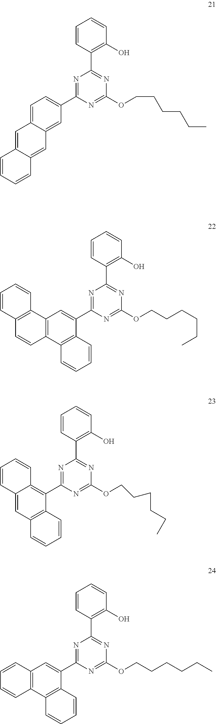


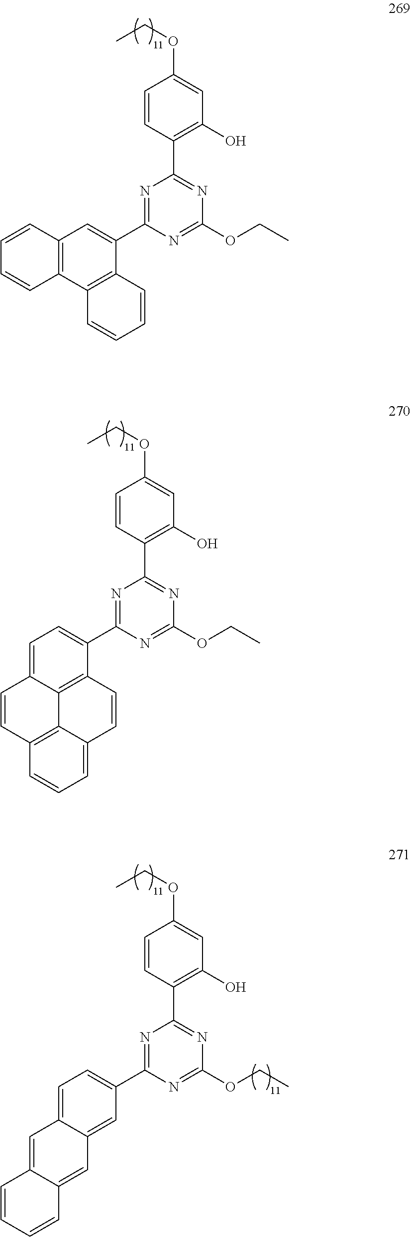


Applications Claiming Priority (9)
| Application Number | Priority Date | Filing Date | Title |
|---|---|---|---|
| KR1020180118701A KR20200039856A (en) | 2018-10-05 | 2018-10-05 | Display device and fused polycyclic compound for organic electroluminescence device |
| KR20180118707 | 2018-10-05 | ||
| KR10-2018-0118704 | 2018-10-05 | ||
| KR10-2018-0118701 | 2018-10-05 | ||
| KR1020180118704A KR20200039857A (en) | 2018-10-05 | 2018-10-05 | Display device and fused polycyclic compound for organic electroluminescence device |
| KR10-2018-0118707 | 2018-10-05 | ||
| KR10-2019-0020685 | 2019-02-21 | ||
| KR1020190020685A KR102726074B1 (en) | 2018-10-05 | 2019-02-21 | Display device and light abosrbing material for the same |
| PCT/KR2019/012652 WO2020071695A1 (en) | 2018-10-05 | 2019-09-27 | Display apparatus and light absorber included in display apparatus |
Related Parent Applications (1)
| Application Number | Title | Priority Date | Filing Date |
|---|---|---|---|
| PCT/KR2019/012652 A-371-Of-International WO2020071695A1 (en) | 2018-10-05 | 2019-09-27 | Display apparatus and light absorber included in display apparatus |
Related Child Applications (1)
| Application Number | Title | Priority Date | Filing Date |
|---|---|---|---|
| US19/076,952 Continuation US20250230132A1 (en) | 2018-10-05 | 2025-03-11 | Display apparatus and light absorber included in display apparatus |
Publications (2)
| Publication Number | Publication Date |
|---|---|
| US20220158099A1 US20220158099A1 (en) | 2022-05-19 |
| US12289992B2 true US12289992B2 (en) | 2025-04-29 |
Family
ID=70055652
Family Applications (2)
| Application Number | Title | Priority Date | Filing Date |
|---|---|---|---|
| US17/250,808 Active 2041-12-29 US12289992B2 (en) | 2018-10-05 | 2019-09-27 | Display apparatus and light absorber included in display apparatus |
| US19/076,952 Pending US20250230132A1 (en) | 2018-10-05 | 2025-03-11 | Display apparatus and light absorber included in display apparatus |
Family Applications After (1)
| Application Number | Title | Priority Date | Filing Date |
|---|---|---|---|
| US19/076,952 Pending US20250230132A1 (en) | 2018-10-05 | 2025-03-11 | Display apparatus and light absorber included in display apparatus |
Country Status (4)
| Country | Link |
|---|---|
| US (2) | US12289992B2 (en) |
| EP (1) | EP3863076B1 (en) |
| JP (3) | JP7525479B2 (en) |
| WO (1) | WO2020071695A1 (en) |
Families Citing this family (2)
| Publication number | Priority date | Publication date | Assignee | Title |
|---|---|---|---|---|
| KR102870803B1 (en) | 2020-08-20 | 2025-10-14 | 삼성디스플레이 주식회사 | Amine compound and light emitting device including the same |
| KR102908971B1 (en) * | 2021-12-02 | 2026-01-08 | 삼성디스플레이 주식회사 | Display device |
Citations (38)
| Publication number | Priority date | Publication date | Assignee | Title |
|---|---|---|---|---|
| US3442898A (en) | 1963-05-04 | 1969-05-06 | Ciba Ltd | Hydroxyaryl-pyrimidines,process for their preparation and their use |
| JPS6124577A (en) | 1984-06-22 | 1986-02-03 | イルフオード アクチエンゲゼルシヤフト | Hydroxyphenyltriazine, manufacture and use as ultraviolet ray absorbent |
| US5096489A (en) | 1989-08-25 | 1992-03-17 | Ciba-Geigy Corporation | Light-stabilized ink compositions |
| US5753729A (en) | 1993-05-17 | 1998-05-19 | Valet; Andreas | Coating compositions stabilized against damage by light, heat, and oxygen |
| KR19990008299A (en) | 1995-05-04 | 1999-01-25 | 워렌리차드보비 | Biological adsorption scaffold |
| KR0178403B1 (en) | 1990-07-23 | 1999-04-01 | 클레에바인 발터; 비틀린 한스-페터 | Aqueous acid solution of poorly soluble UV absorber |
| KR19990072128A (en) | 1995-12-14 | 1999-09-27 | 스타르크, 카르크 | 2- (O- [pyrimidin-4-yl] methyleneoxy) phenyl acetic acid derivative and its use for inhibiting harmful fungi and animal pests |
| KR19990077522A (en) | 1998-03-02 | 1999-10-25 | 시바 스폐셜티 케미칼스 홀딩 인코포레이티드 | NOVEL METHODS FOR THE PREPARATION OF TRIS-ARYL-o-HYDROXYPHENYL-s-TRIAZINES |
| US6111103A (en) | 1998-04-09 | 2000-08-29 | Ciba Specialty Chemicals Corporation | Diresorcinyl-alkoxy- and -aryloxy-s-triazines |
| US20010003363A1 (en) | 1999-12-01 | 2001-06-14 | August Marien | UV-absorbing film and its use as protective sheet |
| KR20010053056A (en) | 1998-06-22 | 2001-06-25 | 마이클 제이. 켈리 | Benzocycle-substituted triazine and pyrimidine ultraviolet light absorbers |
| US20020028937A1 (en) | 1998-06-22 | 2002-03-07 | Cytec Technology Corp. | Benzocycle-substituted triazine and pyrimidine ultraviolet light absorbers |
| US20020171606A1 (en) | 2000-10-17 | 2002-11-21 | Yoshiharu Yabuki | Optical filter having filter layer containing infrared absorbing dye and ultraviolet absorbing agent |
| WO2003035734A1 (en) | 2001-10-18 | 2003-05-01 | Ciba Specialty Chemicals Holding Inc. | Naphthyltriazines as stabilizers for organic material |
| US20030146412A1 (en) * | 2001-11-09 | 2003-08-07 | Gupta Ram Baboo | Phenyl ether-substituted hydroxyphenyl triazine ultraviolet light absorbers |
| KR20050084912A (en) | 2002-10-30 | 2005-08-29 | 시바 스페셜티 케미칼스 홀딩 인크. | Electroluminescent device |
| CN1795232A (en) | 2003-05-26 | 2006-06-28 | 西巴特殊化学品控股有限公司 | Highly compatible and non-migratory polymeric uv-absorber |
| US20070184212A1 (en) | 2006-01-27 | 2007-08-09 | Fujifilm Corporation | Polarizer-protective film, and polarizer and liquid-crystal display device comprising the film |
| KR20080020677A (en) | 2005-06-10 | 2008-03-05 | 시바 스페셜티 케미칼스 홀딩 인크. | Hydroxyphenyltriazines Having Aromatic Carbocyclic Fused Ring Systems |
| KR20130043929A (en) | 2011-10-21 | 2013-05-02 | 엘지디스플레이 주식회사 | Organic light emitting display device |
| US20140203257A1 (en) * | 2013-01-18 | 2014-07-24 | Cheil Industries Inc. | Compound for organic optoelectronic device, organic light emitting diode including the same, and display including the organic light emitting diode |
| WO2014141725A1 (en) | 2013-03-15 | 2014-09-18 | 出光興産株式会社 | Anthracene derivative and organic electroluminescence element using same |
| KR20170050742A (en) | 2015-10-30 | 2017-05-11 | 엘지디스플레이 주식회사 | Liquid Crystal Display Device |
| US9660222B2 (en) | 2012-12-12 | 2017-05-23 | Semiconductor Energy Laboratory Co., Ltd. | Light-emitting device and method for manufacturing the same |
| CN106835693A (en) | 2015-12-07 | 2017-06-13 | 东丽纤维研究所(中国)有限公司 | A kind of antifouling ultraviolet resistant textiles |
| US20170352837A1 (en) * | 2016-06-01 | 2017-12-07 | Samsung Display Co., Ltd. | Display apparatus and method of manufacturing the same |
| KR20170136972A (en) | 2016-06-01 | 2017-12-12 | 삼성디스플레이 주식회사 | Display apparatus and manufacturing method thereof |
| KR20180000913A (en) | 2016-06-24 | 2018-01-04 | 주식회사 엘지화학 | Organic electronic device for virtual reality display |
| KR20180035000A (en) | 2016-09-28 | 2018-04-05 | 엘지디스플레이 주식회사 | Organic light emitting display device |
| KR20180051313A (en) | 2016-11-08 | 2018-05-16 | 엘지디스플레이 주식회사 | Organic light emitting display device |
| US20180203174A1 (en) | 2017-01-13 | 2018-07-19 | Samsung Sdi Co., Ltd. | Polarizing plate for light emitting display apparatus and light emitting display apparatus including the same |
| EP3477722A1 (en) | 2017-10-31 | 2019-05-01 | Samsung Display Co., Ltd. | Light absorber and organic electroluminescence device including the same |
| KR101981294B1 (en) | 2017-10-31 | 2019-05-23 | 삼성디스플레이 주식회사 | Light absorber and organic electroluminescence device including the same |
| US20190229290A1 (en) | 2018-01-24 | 2019-07-25 | Samsung Display Co., Ltd. | Heterocyclic compound and electronic apparatus |
| US20190280064A1 (en) | 2018-03-09 | 2019-09-12 | Samsung Display Co., Ltd. | Electronic apparatus |
| KR20200039856A (en) | 2018-10-05 | 2020-04-17 | 삼성디스플레이 주식회사 | Display device and fused polycyclic compound for organic electroluminescence device |
| KR20200039857A (en) | 2018-10-05 | 2020-04-17 | 삼성디스플레이 주식회사 | Display device and fused polycyclic compound for organic electroluminescence device |
| KR20200040166A (en) | 2018-10-05 | 2020-04-17 | 삼성디스플레이 주식회사 | Display device and light abosrbing material for the same |
-
2019
- 2019-09-27 WO PCT/KR2019/012652 patent/WO2020071695A1/en not_active Ceased
- 2019-09-27 US US17/250,808 patent/US12289992B2/en active Active
- 2019-09-27 EP EP19868585.1A patent/EP3863076B1/en active Active
- 2019-09-27 JP JP2021518150A patent/JP7525479B2/en active Active
-
2023
- 2023-12-21 JP JP2023216073A patent/JP7821152B2/en active Active
-
2025
- 2025-03-11 US US19/076,952 patent/US20250230132A1/en active Pending
- 2025-12-03 JP JP2025227353A patent/JP2026031685A/en not_active Withdrawn
Patent Citations (63)
| Publication number | Priority date | Publication date | Assignee | Title |
|---|---|---|---|---|
| US3442898A (en) | 1963-05-04 | 1969-05-06 | Ciba Ltd | Hydroxyaryl-pyrimidines,process for their preparation and their use |
| JPS6124577A (en) | 1984-06-22 | 1986-02-03 | イルフオード アクチエンゲゼルシヤフト | Hydroxyphenyltriazine, manufacture and use as ultraviolet ray absorbent |
| US5096489A (en) | 1989-08-25 | 1992-03-17 | Ciba-Geigy Corporation | Light-stabilized ink compositions |
| KR0178403B1 (en) | 1990-07-23 | 1999-04-01 | 클레에바인 발터; 비틀린 한스-페터 | Aqueous acid solution of poorly soluble UV absorber |
| US5753729A (en) | 1993-05-17 | 1998-05-19 | Valet; Andreas | Coating compositions stabilized against damage by light, heat, and oxygen |
| KR100361628B1 (en) | 1993-05-17 | 2003-02-11 | 시바 스페셜티 케미칼스 홀딩 인크. | Stabilized paint from damage caused by light, heat and oxygen |
| KR19990008299A (en) | 1995-05-04 | 1999-01-25 | 워렌리차드보비 | Biological adsorption scaffold |
| US6310071B1 (en) | 1995-12-14 | 2001-10-30 | Basf Aktiengesellschaft | 2-(0-(Pyrimidin-4-yl)methyleneoxy)phenylacetic acid derivatives and their use for controlling harmful fungi and animal pests |
| KR19990072128A (en) | 1995-12-14 | 1999-09-27 | 스타르크, 카르크 | 2- (O- [pyrimidin-4-yl] methyleneoxy) phenyl acetic acid derivative and its use for inhibiting harmful fungi and animal pests |
| KR100555072B1 (en) | 1998-03-02 | 2006-02-24 | 시바 스폐셜티 케미칼스 홀딩 인코포레이티드 | Novel Process for Preparing Tris-aryl- (R) -hydroxyphenyl-s-triazine |
| US6242598B1 (en) | 1998-03-02 | 2001-06-05 | Ciba Specialty Chemicals Corporation | Methods for the preparation of tris-aryl-o-hydroxyphenyl-s-triazines |
| KR19990077522A (en) | 1998-03-02 | 1999-10-25 | 시바 스폐셜티 케미칼스 홀딩 인코포레이티드 | NOVEL METHODS FOR THE PREPARATION OF TRIS-ARYL-o-HYDROXYPHENYL-s-TRIAZINES |
| US6111103A (en) | 1998-04-09 | 2000-08-29 | Ciba Specialty Chemicals Corporation | Diresorcinyl-alkoxy- and -aryloxy-s-triazines |
| KR100589869B1 (en) | 1998-04-09 | 2006-06-15 | 시바 스페셜티 케미칼스 홀딩 인크. | Diresorcinyl-alkoxy- and -aryloxy-s-triazines |
| KR20010053056A (en) | 1998-06-22 | 2001-06-25 | 마이클 제이. 켈리 | Benzocycle-substituted triazine and pyrimidine ultraviolet light absorbers |
| US20020028937A1 (en) | 1998-06-22 | 2002-03-07 | Cytec Technology Corp. | Benzocycle-substituted triazine and pyrimidine ultraviolet light absorbers |
| US20010003363A1 (en) | 1999-12-01 | 2001-06-14 | August Marien | UV-absorbing film and its use as protective sheet |
| US20020171606A1 (en) | 2000-10-17 | 2002-11-21 | Yoshiharu Yabuki | Optical filter having filter layer containing infrared absorbing dye and ultraviolet absorbing agent |
| WO2003035734A1 (en) | 2001-10-18 | 2003-05-01 | Ciba Specialty Chemicals Holding Inc. | Naphthyltriazines as stabilizers for organic material |
| JP2005506384A (en) | 2001-10-18 | 2005-03-03 | チバ スペシャルティ ケミカルズ ホールディング インコーポレーテッド | Naphtilriadine as a stabilizer for organic materials |
| CN1571814A (en) | 2001-10-18 | 2005-01-26 | 西巴特殊化学品控股有限公司 | Naphthyl triazines as stabilizers for organic materials |
| US7087753B2 (en) | 2001-10-18 | 2006-08-08 | Ciba Specialty Chemicals Corp. | Naphthyltriazines as stabilizers for organic material |
| US20030146412A1 (en) * | 2001-11-09 | 2003-08-07 | Gupta Ram Baboo | Phenyl ether-substituted hydroxyphenyl triazine ultraviolet light absorbers |
| KR20050084912A (en) | 2002-10-30 | 2005-08-29 | 시바 스페셜티 케미칼스 홀딩 인크. | Electroluminescent device |
| CN1795232A (en) | 2003-05-26 | 2006-06-28 | 西巴特殊化学品控股有限公司 | Highly compatible and non-migratory polymeric uv-absorber |
| US8389719B2 (en) | 2005-06-10 | 2013-03-05 | Ciba Specialty Chemicals Corp. | Hydroxyphenyltriazines with an aromatic carbocyclic fused ring system |
| CN101193870A (en) | 2005-06-10 | 2008-06-04 | 西巴特殊化学品控股有限公司 | Hydroxyphenyltriazines with aromatic carbocyclic fused ring systems |
| JP2008545771A (en) | 2005-06-10 | 2008-12-18 | チバ ホールディング インコーポレーテッド | Hydroxyphenyltriazines containing aromatic carbon fused ring systems |
| US20090136768A1 (en) * | 2005-06-10 | 2009-05-28 | Thomas Vogel | Hydroxyphenyltriazines With An Aromatic Carbocyclic Fused Ring System |
| US8586735B2 (en) | 2005-06-10 | 2013-11-19 | Basf Se | Hydroxyphenyl triazines with an aromatic carbocyclic fused ring system |
| KR101355874B1 (en) | 2005-06-10 | 2014-02-03 | 시바 홀딩 인크 | Hydroxyphenyltriazines with an aromatic carbocyclic fused ring system |
| KR20080020677A (en) | 2005-06-10 | 2008-03-05 | 시바 스페셜티 케미칼스 홀딩 인크. | Hydroxyphenyltriazines Having Aromatic Carbocyclic Fused Ring Systems |
| US20070184212A1 (en) | 2006-01-27 | 2007-08-09 | Fujifilm Corporation | Polarizer-protective film, and polarizer and liquid-crystal display device comprising the film |
| KR20130043929A (en) | 2011-10-21 | 2013-05-02 | 엘지디스플레이 주식회사 | Organic light emitting display device |
| US9660222B2 (en) | 2012-12-12 | 2017-05-23 | Semiconductor Energy Laboratory Co., Ltd. | Light-emitting device and method for manufacturing the same |
| US20140203257A1 (en) * | 2013-01-18 | 2014-07-24 | Cheil Industries Inc. | Compound for organic optoelectronic device, organic light emitting diode including the same, and display including the organic light emitting diode |
| WO2014141725A1 (en) | 2013-03-15 | 2014-09-18 | 出光興産株式会社 | Anthracene derivative and organic electroluminescence element using same |
| KR20170050742A (en) | 2015-10-30 | 2017-05-11 | 엘지디스플레이 주식회사 | Liquid Crystal Display Device |
| KR101744876B1 (en) | 2015-10-30 | 2017-06-08 | 엘지디스플레이 주식회사 | Liquid Crystal Display Device |
| CN106835693A (en) | 2015-12-07 | 2017-06-13 | 东丽纤维研究所(中国)有限公司 | A kind of antifouling ultraviolet resistant textiles |
| US20170352837A1 (en) * | 2016-06-01 | 2017-12-07 | Samsung Display Co., Ltd. | Display apparatus and method of manufacturing the same |
| CN107452752A (en) | 2016-06-01 | 2017-12-08 | 三星显示有限公司 | Display device and its manufacture method |
| KR20170136972A (en) | 2016-06-01 | 2017-12-12 | 삼성디스플레이 주식회사 | Display apparatus and manufacturing method thereof |
| US10707445B2 (en) | 2016-06-01 | 2020-07-07 | Samsung Display Co., Ltd. | Display apparatus and method of manufacturing the same |
| KR20180000913A (en) | 2016-06-24 | 2018-01-04 | 주식회사 엘지화학 | Organic electronic device for virtual reality display |
| KR20180035000A (en) | 2016-09-28 | 2018-04-05 | 엘지디스플레이 주식회사 | Organic light emitting display device |
| KR20180051313A (en) | 2016-11-08 | 2018-05-16 | 엘지디스플레이 주식회사 | Organic light emitting display device |
| US20180203174A1 (en) | 2017-01-13 | 2018-07-19 | Samsung Sdi Co., Ltd. | Polarizing plate for light emitting display apparatus and light emitting display apparatus including the same |
| KR102103589B1 (en) | 2017-10-31 | 2020-04-24 | 삼성디스플레이 주식회사 | Light absorber and organic electroluminescence device including the same |
| EP3477722A1 (en) | 2017-10-31 | 2019-05-01 | Samsung Display Co., Ltd. | Light absorber and organic electroluminescence device including the same |
| US20190131532A1 (en) | 2017-10-31 | 2019-05-02 | Samsung Display Co., Ltd. | Light absorber and organic electroluminescence device including the same |
| CN109721482A (en) | 2017-10-31 | 2019-05-07 | 三星显示有限公司 | Light absorber and organic electroluminescence device including the light absorber |
| KR101981294B1 (en) | 2017-10-31 | 2019-05-23 | 삼성디스플레이 주식회사 | Light absorber and organic electroluminescence device including the same |
| JP2019081756A (en) | 2017-10-31 | 2019-05-30 | 三星ディスプレイ株式會社Samsung Display Co.,Ltd. | Light absorber and organic electroluminescence device including the same |
| KR20200043951A (en) | 2017-10-31 | 2020-04-28 | 삼성디스플레이 주식회사 | Light absorber and organic electroluminescence device including the same |
| EP3517533A2 (en) | 2018-01-24 | 2019-07-31 | Samsung Display Co., Ltd. | Heterocyclic compound and electronic apparatus |
| CN110071095A (en) | 2018-01-24 | 2019-07-30 | 三星显示有限公司 | Heterocyclic compound and electronic device |
| US20190229290A1 (en) | 2018-01-24 | 2019-07-25 | Samsung Display Co., Ltd. | Heterocyclic compound and electronic apparatus |
| CN110246980A (en) | 2018-03-09 | 2019-09-17 | 三星显示有限公司 | Electronic device |
| US20190280064A1 (en) | 2018-03-09 | 2019-09-12 | Samsung Display Co., Ltd. | Electronic apparatus |
| KR20200039856A (en) | 2018-10-05 | 2020-04-17 | 삼성디스플레이 주식회사 | Display device and fused polycyclic compound for organic electroluminescence device |
| KR20200039857A (en) | 2018-10-05 | 2020-04-17 | 삼성디스플레이 주식회사 | Display device and fused polycyclic compound for organic electroluminescence device |
| KR20200040166A (en) | 2018-10-05 | 2020-04-17 | 삼성디스플레이 주식회사 | Display device and light abosrbing material for the same |
Non-Patent Citations (4)
| Title |
|---|
| Chinese Examination report issued on Jan. 26, 2024, from the Chinese Patent Office in corresponding Chinese Patent Application No. 201980065956.0 (12 pages). |
| European Examination Report dated Sep. 3, 2024, in corresponding European Patent Application No. 19 868 585.1 (7 pages). |
| International Search Report for corresponding Application No. PCT/KR2019/012652 dated Jan. 6, 2020, 4pp. |
| Pater, Richard, "Photostable o-Hydroxyphenylquinazolines", Research and Development Division Publication No. 461, vol. 7, (Oct. 1970) JWilmington, Del.19899, pp. 1113-1124 (12 pages). |
Also Published As
| Publication number | Publication date |
|---|---|
| EP3863076A4 (en) | 2022-06-08 |
| EP3863076B1 (en) | 2025-08-06 |
| US20220158099A1 (en) | 2022-05-19 |
| JP7525479B2 (en) | 2024-07-30 |
| JP2026031685A (en) | 2026-02-24 |
| JP7821152B2 (en) | 2026-02-26 |
| JP2024045108A (en) | 2024-04-02 |
| EP3863076A1 (en) | 2021-08-11 |
| US20250230132A1 (en) | 2025-07-17 |
| WO2020071695A1 (en) | 2020-04-09 |
| JP2022504116A (en) | 2022-01-13 |
Similar Documents
| Publication | Publication Date | Title |
|---|---|---|
| KR102726074B1 (en) | Display device and light abosrbing material for the same | |
| US20250230132A1 (en) | Display apparatus and light absorber included in display apparatus | |
| US20250176422A1 (en) | Organic electroluminescence device and organometallic compound for organic electroluminescence device | |
| US20220059771A1 (en) | Organic electroluminescence device and amine compound for organic electroluminescence device | |
| US20220115594A1 (en) | Organic electroluminescence device and amine compound for organic electroluminescence device | |
| US20250056966A1 (en) | Light emitting element and display device including the same | |
| US20240023430A1 (en) | Light emitting element and display device including the same | |
| US12577195B2 (en) | Light emitting element and display device including the same | |
| CN112805844B (en) | Display device and light absorber included in the same | |
| US20230165137A1 (en) | Light emitting element and amine compound for the same | |
| US20220310934A1 (en) | Compound including nitrogen emitting device including the same | |
| US20220123213A1 (en) | Luminescence device and amine compound for organic electroluminescence device | |
| KR102890547B1 (en) | Display device and light abosrbing material for the same | |
| US20260013320A1 (en) | Light emitting element, fused polycyclic compound for the light emitting element, and electronic apparatus including the light emitting element | |
| US20250098529A1 (en) | Light emitting element, amine compound for the same, and display device including the same | |
| US20260101669A1 (en) | Light-emitting element, monoamine compound for the light-emitting element, and electronic apparatus including the light-emitting element | |
| US20260047269A1 (en) | Light emitting element and electronic device including the same | |
| US20250017034A1 (en) | Light-emitting element, display device, and amine compound for the light-emitting element | |
| US20250031575A1 (en) | Light emitting element and polycyclic compound for the same | |
| US20250107313A1 (en) | Light-emitting element, heterocyclic compound for light-emitting element, and electronic device including the light-emitting element | |
| US20230189633A1 (en) | Polycyclic compound, light emitting element including the same, and display device including the same | |
| US12171142B2 (en) | Light emitting device and polycyclic compound for the same | |
| US20260090186A1 (en) | Light-emitting element, hetero compound for light-emitting element, and electronic apparatus including the light-emitting element | |
| US20250366301A1 (en) | Light emitting element, fused polycyclic compound for the same, and electronic apparatus including the same | |
| US20240284796A1 (en) | Light emitting element and fused polycyclic compound for the light emitting element |
Legal Events
| Date | Code | Title | Description |
|---|---|---|---|
| AS | Assignment |
Owner name: SAMSUNG DISPLAY CO., LTD., KOREA, REPUBLIC OF Free format text: ASSIGNMENT OF ASSIGNORS INTEREST;ASSIGNORS:HAN, SANGHYUN;KIM, JONGWOO;JEONG, EUNJAE;AND OTHERS;REEL/FRAME:055500/0739 Effective date: 20210114 |
|
| FEPP | Fee payment procedure |
Free format text: ENTITY STATUS SET TO UNDISCOUNTED (ORIGINAL EVENT CODE: BIG.); ENTITY STATUS OF PATENT OWNER: LARGE ENTITY |
|
| STPP | Information on status: patent application and granting procedure in general |
Free format text: DOCKETED NEW CASE - READY FOR EXAMINATION |
|
| STPP | Information on status: patent application and granting procedure in general |
Free format text: NON FINAL ACTION MAILED |
|
| STPP | Information on status: patent application and granting procedure in general |
Free format text: RESPONSE TO NON-FINAL OFFICE ACTION ENTERED AND FORWARDED TO EXAMINER |
|
| STPP | Information on status: patent application and granting procedure in general |
Free format text: FINAL REJECTION MAILED |
|
| STPP | Information on status: patent application and granting procedure in general |
Free format text: RESPONSE AFTER FINAL ACTION FORWARDED TO EXAMINER |
|
| STPP | Information on status: patent application and granting procedure in general |
Free format text: DOCKETED NEW CASE - READY FOR EXAMINATION |
|
| STPP | Information on status: patent application and granting procedure in general |
Free format text: NOTICE OF ALLOWANCE MAILED -- APPLICATION RECEIVED IN OFFICE OF PUBLICATIONS |
|
| STPP | Information on status: patent application and granting procedure in general |
Free format text: AWAITING TC RESP, ISSUE FEE PAYMENT VERIFIED |
|
| STPP | Information on status: patent application and granting procedure in general |
Free format text: PUBLICATIONS -- ISSUE FEE PAYMENT VERIFIED |
|
| STPP | Information on status: patent application and granting procedure in general |
Free format text: AWAITING TC RESP., ISSUE FEE NOT PAID |
|
| STCF | Information on status: patent grant |
Free format text: PATENTED CASE |
|
| CC | Certificate of correction |