US12278555B2 - Variable gain modulation methods and controllers for AC-DC converter with power factor correction - Google Patents
Variable gain modulation methods and controllers for AC-DC converter with power factor correction Download PDFInfo
- Publication number
- US12278555B2 US12278555B2 US17/973,616 US202217973616A US12278555B2 US 12278555 B2 US12278555 B2 US 12278555B2 US 202217973616 A US202217973616 A US 202217973616A US 12278555 B2 US12278555 B2 US 12278555B2
- Authority
- US
- United States
- Prior art keywords
- gain
- voltage
- mode
- converter
- rectifier circuit
- Prior art date
- Legal status (The legal status is an assumption and is not a legal conclusion. Google has not performed a legal analysis and makes no representation as to the accuracy of the status listed.)
- Active, expires
Links
Images


Classifications
-
- H—ELECTRICITY
- H02—GENERATION; CONVERSION OR DISTRIBUTION OF ELECTRIC POWER
- H02M—APPARATUS FOR CONVERSION BETWEEN AC AND AC, BETWEEN AC AND DC, OR BETWEEN DC AND DC, AND FOR USE WITH MAINS OR SIMILAR POWER SUPPLY SYSTEMS; CONVERSION OF DC OR AC INPUT POWER INTO SURGE OUTPUT POWER; CONTROL OR REGULATION THEREOF
- H02M1/00—Details of apparatus for conversion
- H02M1/42—Circuits or arrangements for compensating for or adjusting power factor in converters or inverters
- H02M1/4208—Arrangements for improving power factor of AC input
-
- H—ELECTRICITY
- H02—GENERATION; CONVERSION OR DISTRIBUTION OF ELECTRIC POWER
- H02M—APPARATUS FOR CONVERSION BETWEEN AC AND AC, BETWEEN AC AND DC, OR BETWEEN DC AND DC, AND FOR USE WITH MAINS OR SIMILAR POWER SUPPLY SYSTEMS; CONVERSION OF DC OR AC INPUT POWER INTO SURGE OUTPUT POWER; CONTROL OR REGULATION THEREOF
- H02M7/00—Conversion of AC power input into DC power output; Conversion of DC power input into AC power output
- H02M7/02—Conversion of AC power input into DC power output without possibility of reversal
- H02M7/04—Conversion of AC power input into DC power output without possibility of reversal by static converters
- H02M7/12—Conversion of AC power input into DC power output without possibility of reversal by static converters using discharge tubes with control electrode or semiconductor devices with control electrode
- H02M7/21—Conversion of AC power input into DC power output without possibility of reversal by static converters using discharge tubes with control electrode or semiconductor devices with control electrode using devices of a triode or transistor type requiring continuous application of a control signal
- H02M7/217—Conversion of AC power input into DC power output without possibility of reversal by static converters using discharge tubes with control electrode or semiconductor devices with control electrode using devices of a triode or transistor type requiring continuous application of a control signal using semiconductor devices only
-
- H—ELECTRICITY
- H02—GENERATION; CONVERSION OR DISTRIBUTION OF ELECTRIC POWER
- H02M—APPARATUS FOR CONVERSION BETWEEN AC AND AC, BETWEEN AC AND DC, OR BETWEEN DC AND DC, AND FOR USE WITH MAINS OR SIMILAR POWER SUPPLY SYSTEMS; CONVERSION OF DC OR AC INPUT POWER INTO SURGE OUTPUT POWER; CONTROL OR REGULATION THEREOF
- H02M1/00—Details of apparatus for conversion
- H02M1/0048—Circuits or arrangements for reducing losses
-
- H—ELECTRICITY
- H02—GENERATION; CONVERSION OR DISTRIBUTION OF ELECTRIC POWER
- H02M—APPARATUS FOR CONVERSION BETWEEN AC AND AC, BETWEEN AC AND DC, OR BETWEEN DC AND DC, AND FOR USE WITH MAINS OR SIMILAR POWER SUPPLY SYSTEMS; CONVERSION OF DC OR AC INPUT POWER INTO SURGE OUTPUT POWER; CONTROL OR REGULATION THEREOF
- H02M1/00—Details of apparatus for conversion
- H02M1/10—Arrangements incorporating converting means for enabling loads to be operated at will from different kinds of power supplies, e.g. from AC or DC
-
- H—ELECTRICITY
- H02—GENERATION; CONVERSION OR DISTRIBUTION OF ELECTRIC POWER
- H02M—APPARATUS FOR CONVERSION BETWEEN AC AND AC, BETWEEN AC AND DC, OR BETWEEN DC AND DC, AND FOR USE WITH MAINS OR SIMILAR POWER SUPPLY SYSTEMS; CONVERSION OF DC OR AC INPUT POWER INTO SURGE OUTPUT POWER; CONTROL OR REGULATION THEREOF
- H02M1/00—Details of apparatus for conversion
- H02M1/14—Arrangements for reducing ripples from DC input or output
- H02M1/15—Arrangements for reducing ripples from DC input or output using active elements
-
- H—ELECTRICITY
- H02—GENERATION; CONVERSION OR DISTRIBUTION OF ELECTRIC POWER
- H02M—APPARATUS FOR CONVERSION BETWEEN AC AND AC, BETWEEN AC AND DC, OR BETWEEN DC AND DC, AND FOR USE WITH MAINS OR SIMILAR POWER SUPPLY SYSTEMS; CONVERSION OF DC OR AC INPUT POWER INTO SURGE OUTPUT POWER; CONTROL OR REGULATION THEREOF
- H02M1/00—Details of apparatus for conversion
- H02M1/42—Circuits or arrangements for compensating for or adjusting power factor in converters or inverters
- H02M1/4208—Arrangements for improving power factor of AC input
- H02M1/4241—Arrangements for improving power factor of AC input using a resonant converter
-
- H—ELECTRICITY
- H02—GENERATION; CONVERSION OR DISTRIBUTION OF ELECTRIC POWER
- H02M—APPARATUS FOR CONVERSION BETWEEN AC AND AC, BETWEEN AC AND DC, OR BETWEEN DC AND DC, AND FOR USE WITH MAINS OR SIMILAR POWER SUPPLY SYSTEMS; CONVERSION OF DC OR AC INPUT POWER INTO SURGE OUTPUT POWER; CONTROL OR REGULATION THEREOF
- H02M3/00—Conversion of DC power input into DC power output
- H02M3/02—Conversion of DC power input into DC power output without intermediate conversion into AC
- H02M3/04—Conversion of DC power input into DC power output without intermediate conversion into AC by static converters
- H02M3/10—Conversion of DC power input into DC power output without intermediate conversion into AC by static converters using discharge tubes with control electrode or semiconductor devices with control electrode
- H02M3/145—Conversion of DC power input into DC power output without intermediate conversion into AC by static converters using discharge tubes with control electrode or semiconductor devices with control electrode using devices of a triode or transistor type requiring continuous application of a control signal
- H02M3/155—Conversion of DC power input into DC power output without intermediate conversion into AC by static converters using discharge tubes with control electrode or semiconductor devices with control electrode using devices of a triode or transistor type requiring continuous application of a control signal using semiconductor devices only
- H02M3/156—Conversion of DC power input into DC power output without intermediate conversion into AC by static converters using discharge tubes with control electrode or semiconductor devices with control electrode using devices of a triode or transistor type requiring continuous application of a control signal using semiconductor devices only with automatic control of output voltage or current, e.g. switching regulators
-
- H—ELECTRICITY
- H02—GENERATION; CONVERSION OR DISTRIBUTION OF ELECTRIC POWER
- H02M—APPARATUS FOR CONVERSION BETWEEN AC AND AC, BETWEEN AC AND DC, OR BETWEEN DC AND DC, AND FOR USE WITH MAINS OR SIMILAR POWER SUPPLY SYSTEMS; CONVERSION OF DC OR AC INPUT POWER INTO SURGE OUTPUT POWER; CONTROL OR REGULATION THEREOF
- H02M1/00—Details of apparatus for conversion
- H02M1/0003—Details of control, feedback or regulation circuits
- H02M1/0016—Control circuits providing compensation of output voltage deviations using feedforward of disturbance parameters
- H02M1/0022—Control circuits providing compensation of output voltage deviations using feedforward of disturbance parameters the disturbance parameters being input voltage fluctuations
-
- H—ELECTRICITY
- H02—GENERATION; CONVERSION OR DISTRIBUTION OF ELECTRIC POWER
- H02M—APPARATUS FOR CONVERSION BETWEEN AC AND AC, BETWEEN AC AND DC, OR BETWEEN DC AND DC, AND FOR USE WITH MAINS OR SIMILAR POWER SUPPLY SYSTEMS; CONVERSION OF DC OR AC INPUT POWER INTO SURGE OUTPUT POWER; CONTROL OR REGULATION THEREOF
- H02M1/00—Details of apparatus for conversion
- H02M1/42—Circuits or arrangements for compensating for or adjusting power factor in converters or inverters
- H02M1/4208—Arrangements for improving power factor of AC input
- H02M1/4233—Arrangements for improving power factor of AC input using a bridge converter comprising active switches
-
- H—ELECTRICITY
- H02—GENERATION; CONVERSION OR DISTRIBUTION OF ELECTRIC POWER
- H02M—APPARATUS FOR CONVERSION BETWEEN AC AND AC, BETWEEN AC AND DC, OR BETWEEN DC AND DC, AND FOR USE WITH MAINS OR SIMILAR POWER SUPPLY SYSTEMS; CONVERSION OF DC OR AC INPUT POWER INTO SURGE OUTPUT POWER; CONTROL OR REGULATION THEREOF
- H02M1/00—Details of apparatus for conversion
- H02M1/42—Circuits or arrangements for compensating for or adjusting power factor in converters or inverters
- H02M1/4208—Arrangements for improving power factor of AC input
- H02M1/4258—Arrangements for improving power factor of AC input using a single converter stage both for correction of AC input power factor and generation of a regulated and galvanically isolated DC output voltage
-
- H—ELECTRICITY
- H02—GENERATION; CONVERSION OR DISTRIBUTION OF ELECTRIC POWER
- H02M—APPARATUS FOR CONVERSION BETWEEN AC AND AC, BETWEEN AC AND DC, OR BETWEEN DC AND DC, AND FOR USE WITH MAINS OR SIMILAR POWER SUPPLY SYSTEMS; CONVERSION OF DC OR AC INPUT POWER INTO SURGE OUTPUT POWER; CONTROL OR REGULATION THEREOF
- H02M3/00—Conversion of DC power input into DC power output
- H02M3/01—Resonant DC/DC converters
-
- H—ELECTRICITY
- H02—GENERATION; CONVERSION OR DISTRIBUTION OF ELECTRIC POWER
- H02M—APPARATUS FOR CONVERSION BETWEEN AC AND AC, BETWEEN AC AND DC, OR BETWEEN DC AND DC, AND FOR USE WITH MAINS OR SIMILAR POWER SUPPLY SYSTEMS; CONVERSION OF DC OR AC INPUT POWER INTO SURGE OUTPUT POWER; CONTROL OR REGULATION THEREOF
- H02M3/00—Conversion of DC power input into DC power output
- H02M3/22—Conversion of DC power input into DC power output with intermediate conversion into AC
- H02M3/24—Conversion of DC power input into DC power output with intermediate conversion into AC by static converters
- H02M3/28—Conversion of DC power input into DC power output with intermediate conversion into AC by static converters using discharge tubes with control electrode or semiconductor devices with control electrode to produce the intermediate AC
- H02M3/325—Conversion of DC power input into DC power output with intermediate conversion into AC by static converters using discharge tubes with control electrode or semiconductor devices with control electrode to produce the intermediate AC using devices of a triode or a transistor type requiring continuous application of a control signal
- H02M3/335—Conversion of DC power input into DC power output with intermediate conversion into AC by static converters using discharge tubes with control electrode or semiconductor devices with control electrode to produce the intermediate AC using devices of a triode or a transistor type requiring continuous application of a control signal using semiconductor devices only
- H02M3/33569—Conversion of DC power input into DC power output with intermediate conversion into AC by static converters using discharge tubes with control electrode or semiconductor devices with control electrode to produce the intermediate AC using devices of a triode or a transistor type requiring continuous application of a control signal using semiconductor devices only having several active switching elements
- H02M3/33571—Half-bridge at primary side of an isolation transformer
-
- H—ELECTRICITY
- H02—GENERATION; CONVERSION OR DISTRIBUTION OF ELECTRIC POWER
- H02M—APPARATUS FOR CONVERSION BETWEEN AC AND AC, BETWEEN AC AND DC, OR BETWEEN DC AND DC, AND FOR USE WITH MAINS OR SIMILAR POWER SUPPLY SYSTEMS; CONVERSION OF DC OR AC INPUT POWER INTO SURGE OUTPUT POWER; CONTROL OR REGULATION THEREOF
- H02M3/00—Conversion of DC power input into DC power output
- H02M3/22—Conversion of DC power input into DC power output with intermediate conversion into AC
- H02M3/24—Conversion of DC power input into DC power output with intermediate conversion into AC by static converters
- H02M3/28—Conversion of DC power input into DC power output with intermediate conversion into AC by static converters using discharge tubes with control electrode or semiconductor devices with control electrode to produce the intermediate AC
- H02M3/325—Conversion of DC power input into DC power output with intermediate conversion into AC by static converters using discharge tubes with control electrode or semiconductor devices with control electrode to produce the intermediate AC using devices of a triode or a transistor type requiring continuous application of a control signal
- H02M3/335—Conversion of DC power input into DC power output with intermediate conversion into AC by static converters using discharge tubes with control electrode or semiconductor devices with control electrode to produce the intermediate AC using devices of a triode or a transistor type requiring continuous application of a control signal using semiconductor devices only
- H02M3/33569—Conversion of DC power input into DC power output with intermediate conversion into AC by static converters using discharge tubes with control electrode or semiconductor devices with control electrode to produce the intermediate AC using devices of a triode or a transistor type requiring continuous application of a control signal using semiconductor devices only having several active switching elements
- H02M3/33573—Full-bridge at primary side of an isolation transformer
-
- H—ELECTRICITY
- H02—GENERATION; CONVERSION OR DISTRIBUTION OF ELECTRIC POWER
- H02M—APPARATUS FOR CONVERSION BETWEEN AC AND AC, BETWEEN AC AND DC, OR BETWEEN DC AND DC, AND FOR USE WITH MAINS OR SIMILAR POWER SUPPLY SYSTEMS; CONVERSION OF DC OR AC INPUT POWER INTO SURGE OUTPUT POWER; CONTROL OR REGULATION THEREOF
- H02M7/00—Conversion of AC power input into DC power output; Conversion of DC power input into AC power output
- H02M7/02—Conversion of AC power input into DC power output without possibility of reversal
- H02M7/04—Conversion of AC power input into DC power output without possibility of reversal by static converters
- H02M7/12—Conversion of AC power input into DC power output without possibility of reversal by static converters using discharge tubes with control electrode or semiconductor devices with control electrode
- H02M7/21—Conversion of AC power input into DC power output without possibility of reversal by static converters using discharge tubes with control electrode or semiconductor devices with control electrode using devices of a triode or transistor type requiring continuous application of a control signal
- H02M7/217—Conversion of AC power input into DC power output without possibility of reversal by static converters using discharge tubes with control electrode or semiconductor devices with control electrode using devices of a triode or transistor type requiring continuous application of a control signal using semiconductor devices only
- H02M7/219—Conversion of AC power input into DC power output without possibility of reversal by static converters using discharge tubes with control electrode or semiconductor devices with control electrode using devices of a triode or transistor type requiring continuous application of a control signal using semiconductor devices only in a bridge configuration
-
- Y—GENERAL TAGGING OF NEW TECHNOLOGICAL DEVELOPMENTS; GENERAL TAGGING OF CROSS-SECTIONAL TECHNOLOGIES SPANNING OVER SEVERAL SECTIONS OF THE IPC; TECHNICAL SUBJECTS COVERED BY FORMER USPC CROSS-REFERENCE ART COLLECTIONS [XRACs] AND DIGESTS
- Y02—TECHNOLOGIES OR APPLICATIONS FOR MITIGATION OR ADAPTATION AGAINST CLIMATE CHANGE
- Y02B—CLIMATE CHANGE MITIGATION TECHNOLOGIES RELATED TO BUILDINGS, e.g. HOUSING, HOUSE APPLIANCES OR RELATED END-USER APPLICATIONS
- Y02B70/00—Technologies for an efficient end-user side electric power management and consumption
- Y02B70/10—Technologies improving the efficiency by using switched-mode power supplies [SMPS], i.e. efficient power electronics conversion e.g. power factor correction or reduction of losses in power supplies or efficient standby modes
-
- Y—GENERAL TAGGING OF NEW TECHNOLOGICAL DEVELOPMENTS; GENERAL TAGGING OF CROSS-SECTIONAL TECHNOLOGIES SPANNING OVER SEVERAL SECTIONS OF THE IPC; TECHNICAL SUBJECTS COVERED BY FORMER USPC CROSS-REFERENCE ART COLLECTIONS [XRACs] AND DIGESTS
- Y02—TECHNOLOGIES OR APPLICATIONS FOR MITIGATION OR ADAPTATION AGAINST CLIMATE CHANGE
- Y02T—CLIMATE CHANGE MITIGATION TECHNOLOGIES RELATED TO TRANSPORTATION
- Y02T10/00—Road transport of goods or passengers
- Y02T10/60—Other road transportation technologies with climate change mitigation effect
- Y02T10/70—Energy storage systems for electromobility, e.g. batteries
-
- Y—GENERAL TAGGING OF NEW TECHNOLOGICAL DEVELOPMENTS; GENERAL TAGGING OF CROSS-SECTIONAL TECHNOLOGIES SPANNING OVER SEVERAL SECTIONS OF THE IPC; TECHNICAL SUBJECTS COVERED BY FORMER USPC CROSS-REFERENCE ART COLLECTIONS [XRACs] AND DIGESTS
- Y02—TECHNOLOGIES OR APPLICATIONS FOR MITIGATION OR ADAPTATION AGAINST CLIMATE CHANGE
- Y02T—CLIMATE CHANGE MITIGATION TECHNOLOGIES RELATED TO TRANSPORTATION
- Y02T10/00—Road transport of goods or passengers
- Y02T10/60—Other road transportation technologies with climate change mitigation effect
- Y02T10/7072—Electromobility specific charging systems or methods for batteries, ultracapacitors, supercapacitors or double-layer capacitors
-
- Y—GENERAL TAGGING OF NEW TECHNOLOGICAL DEVELOPMENTS; GENERAL TAGGING OF CROSS-SECTIONAL TECHNOLOGIES SPANNING OVER SEVERAL SECTIONS OF THE IPC; TECHNICAL SUBJECTS COVERED BY FORMER USPC CROSS-REFERENCE ART COLLECTIONS [XRACs] AND DIGESTS
- Y02—TECHNOLOGIES OR APPLICATIONS FOR MITIGATION OR ADAPTATION AGAINST CLIMATE CHANGE
- Y02T—CLIMATE CHANGE MITIGATION TECHNOLOGIES RELATED TO TRANSPORTATION
- Y02T90/00—Enabling technologies or technologies with a potential or indirect contribution to GHG emissions mitigation
- Y02T90/10—Technologies relating to charging of electric vehicles
- Y02T90/14—Plug-in electric vehicles
Definitions
- the invention relates generally to the field of AC-DC converters. More specifically, the invention relates to controllers and control methods for AC-DC converters that implement two or more operating modes, wherein each operating mode determines a gain of the converter rectifier circuit and the AC-DC converter provides a wide range of DC output voltage with power factor correction.
- the DC output voltage contains a ripple voltage with a ripple frequency lower than an AC line frequency.
- the output DC voltage is regulated to the required value by alternatingly operating the rectifier circuit between full-bridge mode and half-bridge mode when input AC voltage is between the low range and the high range.
- the output DC voltage is regulated to the required value by changing the gain of the rectifier circuit when it is operating in full-bridge mode.
- the rectifier circuit operates in half-bridge mode for a first integer value of the half-line period of the AC input voltage and stops operating for a second integer value of the half-line period of the AC input voltage.
- the rectifier circuit is operating when an instantaneous AC input voltage is at or close to its peak value and the rectifier circuit is not operating when the instantaneous AC input voltage is at or close to its zero-crossing value.
- the rectifier circuit is operating during a first portion of the AC input voltage half line cycle when an instantaneous AC input voltage is from 0 to 45 degrees or from 135 to 180 degrees from an AC input peak voltage value and the rectifier circuit is not operating for the rest of the AC input voltage half line cycle.
- the controller is implemented at least in part in computer-executable instructions stored on non-transitory computer-readable storage media, and the controller includes a computer or other processor that executes the stored instructions.
- an AC-DC converter comprising a controller in accordance with embodiments described herein.
- a method for controlling an AC-DC converter comprising using a controller comprising control logic to control a rectifier circuit of the AC-DC converter according to two or more operating modes; wherein each operating mode of the two or more operating modes determines a gain of the rectifier circuit; wherein the controller selects an operating mode from the two or more operating modes based on at least one of an AC input voltage value and a required DC output voltage value; wherein the AC-DC converter provides a wide range of DC output voltage with power factor correction.
- the high-gain mode, low-gain mode, and zero-gain mode are alternatively implemented by the controller.
- the controller controls the rectifier circuit to operate in first and second modes; wherein the rectifier circuit operates in the first mode for a first integer value of a half-line period of the AC input voltage and the rectifier circuit operates in the second mode for a second integer value of the half-line period of the AC input voltage.
- an LLC converter is used as the rectifier circuit.
- the DC output voltage of the AC-DC converter contains a low frequency ripple voltage; wherein a frequency of the ripple voltage is related to the frequency of the AC input line voltage.
- the rectifier circuit is in full-bridge mode when the input AC voltage is in a low range; the rectifier circuit is in half-bridge mode when the input AC voltage is in a high-range; the output DC voltage is regulated to a required DC value by changing the gain of the rectifier circuit in the full-bridge mode when input voltage is in the low range; the output DC voltage is regulated to the required DC value by changing the gain of the rectifier circuit in the half-bridge mode when input AC voltage is in the high range.
- the output DC voltage is regulated to the required value by alternatingly operating the rectifier circuit between full-bridge mode and half-bridge mode when input AC voltage is between the low range and the high range.
- the rectifier circuit operates in full-bridge mode for one integer value of the half-line period of the AC input voltage and stops operating for another integer value of half-line period of the AC input voltage.
- the rectifier circuit operates in half-bridge mode for a first integer value of the half-line period of the AC input voltage and stops operating for a second integer value of the half-line period of the AC input voltage.
- the output DC voltage is regulated to the required value by changing the gain of the rectifier circuit operating in half-bridge mode.
- the controller controls the rectifier circuit so that the rectifier circuit is operating for a first portion of the AC input voltage half line period and the rectifier circuit is not operating for a second portion of the AC input voltage half line period.
- the rectifier circuit is operating when an instantaneous AC input voltage is at or close to its peak value and the rectifier circuit is not operating when the instantaneous AC input voltage is at or close to its zero-crossing value.
- the rectifier circuit is operating when an instantaneous AC input voltage is at its peak value ⁇ 45 degrees and the rectifier circuit is not operating when the instantaneous AC input voltage is at its zero-crossing value ⁇ 45 degrees.
- the output DC voltage is regulated by controlling AC input power to the rectifier circuit during a time interval when the rectifier circuit is operating.
- the output DC voltage is regulated by controlling a duration of a time interval when the rectifier circuit is operating.
- the AC-DC converter may be a boost converter, isolated boost converter, PWM converter, LLC resonant converter, or LCC resonant converter.
- non-transitory computer readable media for use with a processor, the computer readable media having stored thereon instructions that direct the processor to execute processing steps including controlling a rectifier circuit of an AC-DC converter in accordance with embodiments described herein.
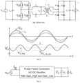
- FIG. 1 is a circuit diagram of a boost converter followed by a LLC converter for an AC-DC power supply, according to the prior art.
- FIG. 3 is a circuit diagram of a full-bridge pulse width modulation (PWM) converter, according to the prior art.
- PWM pulse width modulation
- FIG. 4 a circuit diagram of a full-bridge LLC DC-DC converter, according to the prior art.
- FIG. 5 is a plot of AC input voltage, AC input current, and output voltage waveforms of an AC to DC converter with power factor correction (PFC), according to the prior art.
- PFC power factor correction
- FIG. 6 is generalized circuit block diagram of an AC-DC rectifier with power factor correction showing the output hold up capacitor and constant current load, according to one embodiment.
- FIG. 21 B is a control block diagram for controlling an LLC converter to achieve PFC operation.
- FIG. 22 is a control block diagram for an AC-DC rectifier, according to one embodiment.
- FIG. 26 shows waveforms for inner-line frequency modulation implemented for an LLC converter, wherein the converter is on from 60-degree to 120-degree, according to one embodiment.
- Described herein are controllers and circuits for an AC-DC rectifier for applications with large input and output voltage variation range, wherein the AC-DC rectifier has two or more voltage gains and the AC-DC rectifier performs under optimal operating condition over the entire input and output voltage variation range.
- a characteristic, parameter, and/or value that is substantially absent may be one that is within the noise, beneath background, below detection limits, or a small fraction (e.g., ⁇ 1%, ⁇ 0.1%, ⁇ 0.01%, ⁇ 0.001%, ⁇ 0.00001%, ⁇ 0.000001%, ⁇ 0.0000001%) of the significant characteristic. It is understood that a characteristic, parameter, and/or value that is referred to herein as being the “same” as another characteristic, parameter, and/or value may be substantially the same as the other characteristic, parameter, and/or value.
- a controller may be implemented to control operation of the converter, which may include implementing a gain modulation strategy as described herein.
- the controller may perform one or more operations such as, for example, but not limited to, input and/or output voltage and/or current sensing, generating voltage and/or current reference signals, power factor correction, and generating gate drive signals for switches (e.g., MOSFETs, IGBTs, etc.) of the converter.
- switches e.g., MOSFETs, IGBTs, etc.
- the memory may include various forms of non-volatile (i.e., non-transitory) memory including flash memory or read only memory (ROM) including various forms of programmable read only memory (e.g., PROM, EPROM, EEPROM) and/or volatile memory including random access memory (RAM) including static random access memory (SRAM), dynamic random access memory (DRAM) and synchronous dynamic random access memory (SDRAM).
- ROM read only memory
- PROM programmable read only memory
- RAM random access memory
- SRAM static random access memory
- DRAM dynamic random access memory
- SDRAM synchronous dynamic random access memory
- a converter may include a driver circuit or device to interface between outputs of the controller and the control (e.g., gate) terminals of the semiconductor switches.
- the memory stores executable code including control logic which is configured to control the overall operation of a converter in accordance with a desired control strategy, such as a converter gain modulation strategy as described herein.
- control logic when executed by the processor, is configured to generate, in response to one or more input signals, the various gate drive signals for the switches of the converter.
- the control logic may include programmed logic blocks to implement specific functions, for example, including without limitation, zero crossing detection, error amplifier, pulse width modulation (PWM), power factor correction (PFC), zero voltage switching (ZVS), rms voltage and/or current calculator, operating mode control logic, and startup and/or shut down strategy.
- the memory may also store features, e.g., a lookup table that may be accessed by the control logic.
- a modulation strategy includes changing the voltage gain from one AC line cycle to the next AC line cycle, referred to herein as sub-line frequency modulation, or as sub-F_line modulation. This may include changing the operation mode of the converter at a frequency lower than the line frequency (or AC line frequency, 50 Hz in Asia, Europe and 60 Hz in North America). Operation modes may include high voltage gain, low voltage gain, and zero voltage gain.
- the sub-F_line modulation frequency (F_lineM) is lower than the AC line frequency, such as 10 Hz or 20 Hz.
- sub-switching frequency modulation the operation mode of the converter is changed at a frequency that is lower than the switching frequency and higher than the AC line frequency.
- the line frequency may be 50 Hz or 60 Hz
- the switching frequency may be 500 kHz.
- the sub-Fs modulation frequency (F_SM) may be, e.g., about 20 kHz.
- T_SM the converter operates according to one of three possible modes: high voltage gain, low voltage gain, and zero voltage gain.
- PFC Power Factor Correction
- the boost converter operates in voltage doubler mode.
- the VD boost converter can operate at two voltage gains with the same duty cycle. It is noted that in the above example, the VD boost converter has two possible operation modes.
- FIG. 4 is a circuit diagram of a full-bridge LLC converter according to the prior art.
- Cr, Lr, and Lp are resonant components and Q 1 , Q 2 , Q 3 , and Q 4 are the switches of the full-bridge configuration.
- the secondary side is a full wave rectifier with diode bridge.
- a half wave rectifier with center tapped transformer can also be used.
- a synchronous rectifier (SR) can be used to replace the diodes to reduce the loss of the secondary side circuit.
- SR synchronous rectifier
- the transformer turns ratio (n) n [ 1 + 1 K ⁇ ( 1 - 1 fn 2 ) ] + Q 2 ( f n - 1 fn ) 2 ( 6 )
- the transformer turns ratio (n) series resonant frequency (f r ), normalized frequency (f n ), inductance ratio (K), and quality factor (Q) are as follows:
- the duty cycle of a boost converter is about 50%, it can be considered as optimal operating condition. However, if the duty cycle is about 90%, it cannot be considered as optimal operating condition because the voltage and current stress for the switches will be very high.
- full-bridge PWM converter and full-bridge LLC converter if all the MOSFETs are turned off all the time, the converter does not operate, and the output voltage and gain will be zero. This mode of operation is considered as zero-gain mode.
- boost converter if the MOSFETs are turned off, the output voltage will equal to input voltage and the gain is one (1).
- the AC input current follows the AC input voltage, in same phase and same shape, as shown in FIG. 5 . Since the input power is changing over time and the output load draws constant power, an energy storage component is needed.
- the energy storage component is usually a large capacitor.
- the energy storage capacitor is C BST . Since C BST is usually very large, voltage across C BST is a DC value (Vo_avg) with a small low frequency voltage ripple (Vo_rip_pp).
- the ripple frequency is two times the line frequency (100 Hz or 120 Hz).
- the value of Vo_avg is much larger than the value of Vo_rip_pp.
- Variable Gain Modulation control to achieve very wide output voltage variation while maintaining desired, or optimal, operating conditions for the switching converter (also referred to as an AC-DC rectifier when the input is an AC voltage).
- Variable Gain Modulation includes:
- the time interval when the switching power converter operates at either high-gain mode or low-gain mode may be selected so that the output voltage is rising at high-gain mode operation and falling at low-gain mode operation, for example, such as shown in the simulation waveforms in FIG. 8 and FIG. 9 .
- FIG. 6 is a block diagram of an AC-DC rectifier with two voltage gains: Gain_high and Gain_low, with power factor correction (PFC), according to one embodiment.
- PFC power factor correction
- a relatively large capacitor Co as shown in FIG. 6
- Co 1,000 uF is used in the analysis and simulation, although other values may of course be used.
- the value of the ripple voltage (Vo_rip_pp) is small as compared with its DC value (Vo_avg), normally less than about 20% of the DC value.
- the frequency of the ripple voltage is related to the line frequency.
- An AC-DC rectifier with power factor correction has two operation modes: (1) high-gain operation mode and (2) low-gain operation mode.
- sub-line frequency modulation will change the DC value of the output voltage of a converter with power factor correction. It will not remove the low frequency ripple voltage of the converter. Another DC-DC converter will be needed to remove the low frequency ripple voltage to produce a pure DC voltage.
- the optimal operation such as high efficiency mode operation, will be maintained over a limited range of gain values.
- the high efficiency mode operation may be maintained for a voltage gain range of 1.8 to 2.2, or a variation of ⁇ 10%. Therefore, the DC value of the output voltage of the converter may be regulated accurately to a desired value by changing the actual gain of the converter.
- Gain_high the gain value under high-gain mode operation
- the output voltage of the converter may be regulated based on the following relationship:
- a difference between sub-line frequency modulation and sub-double-line frequency modulation is the minimum time interval.
- the minimum interval is half the line period.
- the minimum interval is 10 ms.
- the minimum interval is 8.33 ms.
- T 3 about 2.17 second
- T_half_line is the half line period.
- sub-double-line frequency modulation has features of the sub-line frequency modulation method, while achieving much smaller (almost reduced by half) low frequency ripple voltage. Therefore, sub-double-line frequency modulation method may be a preferred implementation method. In the rest of this description, only sub-double-line frequency modulation will be discussed.
- the steady state output voltage would be 400V (200V*2) for high-gain mode operation and 200V (200V*1) for low-gain mode operation.
- the output voltage may be regulated between 200V and 400V, or between the steady state output voltage values of the high-gain mode operation and low-gain mode operation.
- N_zero is the number of AC line cycles when the converter operates at zero-gain operation mode. When there is no energy transfer from input to output, the output voltage will be zero in steady state.
- N_half_zero is the number of AC half-line cycles when the AC-DC rectifier operates at zero-gain mode.
- the output voltage of the AC-DC rectifier may be regulated at about 150V.
- an AC line frequency of 50 Hz is used for illustration purposes.
- the AC-DC rectifier operates at PFC mode.
- the output voltage is regulated at 150V DC and the DC load current is 5 A over the above input voltage variation (between 100 Vrms and 200 Vrms). Therefore, the output power is 750 W.
- the load resistor is 300.
- load current is always 5 A.
- the average value of the output voltage is regulated at 150V when the input AC voltage changes from 100V to 200V.
- FIG. 19 shows simulated operation waveforms.
- the average value of the output voltage is regulated at 150V.
- Step 2 The desired output voltage is determined, Vo_avg.
- Vo_avg is between Vo_avg_min and Vo_avg_max.
- Step 5 If condition 1 as shown in equation (12.1) is satisfied, step 6 may be used to determine the control parameters. If condition 2 as shown in equation (12.2) is satisfied, step 7 may be used to determine the control parameters.
- Step 6.1 Determine N_L and N_Z (e.g., based on a look up table with the measured Vin and desired Vo_avg value) so that the output voltage is close to the required output voltage, Vo_avg.
- the look-up table may be generated based on the design requirement and low-gain value.
- Step 6.2 With the N_L and N_Z obtained in Step 6.1, change the value of the low-gain of the AC-DC Rectifier to produce the desired output voltage, Vo_avg. This may be performed by a feedback circuit.
- the AC-DC rectifier may operate at high-gain mode all the time without operating at low-gain mode. This may happen when the input voltage is low, and the required output voltage is high.
- the output voltage may be regulated to the designed value by changing the value of Gain_high.
- the AC-DC rectifier may operate at low-gain mode all the time without operating at high-gain mode. This may happen when the input voltage is high, and the required output voltage is low.
- the output voltage may be regulated to the desired value by changing the value of Gain_low.
- Gain_high The high-gain value, Gain_high, is two times the low-gain value, Gain_low.
- Gain_high 2*Gain_low.
- variable gain modulation strategy may be implemented as follows:
- Step 7.4.1 When input voltage is between 100V and 140V, the AC-DC rectifier operates only at high-gain mode.
- the output voltage may be controlled by changing the gain value of Gain_high.
- Step 7.4.3 When the input voltage is between 190V and 240V, the AC-DC rectifier operates only at low-gain mode.
- the output voltage may be controlled by changing the gain value of Gain_low.
- Step 7.4.6 With the design obtained in step 7.4.5, the AC-DC rectifier operates at high-gain mode when input voltage is low (100-140V) and operate at low-gain mode when the input voltage is high (190-240V) and produces the required output voltage (50V) by changing the voltage gain value of the rectifier.
- the output voltage should also be regulated at 50V when the input voltage is between 140V and 190V, or it is required that the output voltage should be maintained at 50V when the input voltage is at any value between 100V to 240V, the following control strategies may be used:
- Condition #2 When the input voltage is between 190V and 240V, the AC-DC rectifier operates at low-gain mode and the low-gain value is used to regulate the output voltage to the designed value, 50V.
- Condition #3 When the input voltage is between 140V and 190V, sub-double-line frequency modulation may be used.
- the AC-DC rectifier operates alternatively between high-gain mode and low-gain mode.
- the N_L and N_H value, as well as high-gain value and low-gain value are used to regulate the output voltage to the designed value, 50V. Detailed control methods are described above.
- control strategy may be implemented in different converter topologies.
- various topologies such as full-bridge PWM converter, full-bridge LLC resonant converter, can operate at two voltage gains when they operate at full-bridge mode (high-gain mode) and half-bridge mode (low-gain mode). Operation under two voltage gains may be optimized for the specific converter topology used.
- This section describes implementation of the variable gain modulation control strategy for a LLC converter.
- Gain_LLC_FB 2*Gain_LLC_HB (19)
- Zero-gain mode operation of an LLC AC-DC rectifier may be achieved when all four switches stop switching (i.e., the switches are off).
- FIG. 21 A is a circuit diagram of an LLC converter used as an AC-DC rectifier with power factor correction.
- the AC input voltage is rectified by the diode bridge.
- the rectified AC voltage (Vrec) is applied to the input of the LLC converter.
- FIG. 21 B is a controller block diagram for controlling the LLC converter to achieve PFC operation.
- the output of the voltage error amplifier is the current reference for the input LLC current.
- the switching frequency of the LLC converter is changed so that the LLC input current is a rectified sinusoidal waveform with required peak value, determined by Iref.
- Step 5.11 When the input voltage is between 100V to 140V, the LLC AC-DC rectifier operates at full-bridge mode. The output voltage is controlled by changing the gain of the full-bridge LLC rectifier, Gain_LLC_FB.
- Gain_LLC_FB 0.45 (24.1)
- Gain_LLC_HB 0.21 (24.2)
- the output voltage may be regulated at any value between 40V and 60V when the input voltage changes from 100V to 240V, even though the gain variation of LLC AC-DC rectifier is ⁇ 10%.
- N_LLC_FB and N_LLC_HB may be obtained by, e.g., a look up table based on the input voltage, Vin, output voltage, Vo_avg, and the Gain_LLC_FB, Gain_LLC_HB. Vin can be measured from the input.
- Vo_avg may be obtained from the system, and Gain_LLC_FB and Gain_LLC_HB are known after the design is completed.
- a closed loop control circuit may be used to change the switching frequency of the LLC AC-DC rectifier so that the desired output voltage, Vo_avg, is obtained.
- FIG. 22 is a block diagram of a controller that may be implemented for an LLC AC-DC rectifier over wide input voltage variation range to achieve the control strategy described above, according to one embodiment.
- the appropriate mode control signal (dashed line) is sent to the gate driver block 2230 of the controller that generates the gate drive signals G 1 to G 4 for the converter switches to implement the mode in the converter.
- the five modes of the gate driver block are shown separately as Controller 1 to Controller 5, however, it will be appreciated that in an actual implementation there is one gate driver block 2230 that receives the mode control signal corresponding to the selected mode from the mode selector.
- controller 1 determines the switching frequency based on the output voltage and reference voltage so that the output voltage Vo is regulated to the reference voltage Vref.
- the input voltage may be monitored all the time.
- the controller generates four gate drive signals for the switches (MOSFETs) of the LLC AC-DC rectifier (e.g., as shown in FIG. 21 A ).
- Fs_HB is the switching frequency of the LLC converter when operating at half-bridge mode.
- controller 5 determines N_FB, N_ZG, and Fs_FB, based on the output voltage and reference voltage so that the output voltage Vo is regulated to the reference voltage Vref.
- the input voltage may be monitored all the time.
- the controller generates gate drive signals for the MOSFETs of LLC AC-DC rectifier as shown in FIG. 21 A . It is noted that in most cases, the combination of half-bridge and Zero-Gain mode operation is preferred over the combination of full-bridge and Zero-Gain mode operation because an output voltage that is lower than the half-bridge mode of operation is required in this case.
- the N_FB, N_HB, and N_ZG may be selected based on Vac, Vref, and Vo by a look up table since the selection is limited.
- the actual output voltage Vo may be regulated by the switching frequency, Fs_FB and Fs_HB by a feedback loop.
- the mode selection block will change one operation mode to the other.
- the mode change may occur at zero crossing point of the input AC voltage.
- control diagram shown in FIG. 22 may also be implemented for any AC-DC rectifier based on other circuit topologies.
- the sub-double-line frequency modulation method will produce a low frequency ripple with frequency lower than the double line frequency, such as 25 Hz in the case of 50 Hz line frequency AC system.
- the output voltage may be reduced while the low frequency ripple is maintained at double line frequency.
- LLC converter When LLC converter operates, it can operate at either full-bridge or half-bridge mode.
- the turn-on operation of the LLC AC-DC rectifier does not need to be symmetrical to the 90-degree point (the peak value of the AC voltage).
- it may be asymmetrical to 90-degree point, such as from 50-degree to 110-degree or from 70-degree to 140-degree.
- FIG. 25 shows another example of an implementation of inner-line frequency modulation when the LLC converter operates (is turned on) between 0-degree to 60-degree and does not operate (is turned off) between 61-degree and 179-degree.
- the output voltage (V53) will be lower than the above two cases.
- the input current is controlled to follow the input voltage waveform when the LLC converter is turned on (in operation). It is a portion of the sinusoidal waveform.
- the input current is zero when LLC converter is off (not in operation.
- the output voltage which is determined by the input power, may also be controlled by the peak current when LLC converter is on.
- the inner-line frequency modulation method may also be applied to other AC-DC converter topologies, such as boost converter, isolated boost converter, as well as LCC resonant converters.
- boost converter operates at AC-DC rectifier
- the output voltage is higher than the peak AC line voltage. Therefore, when the boost switch stops switching, the boost diode will be reverse biased, and no energy will be transferred from AC side to the output DC side.
- boost converter and LLC converter A slight difference between boost converter and LLC converter is that the inductance value of the boost inductor is much larger than the resonant inductor in LLC converter. During the transition between on operation and off operation, the energy stored in the boost inductor will be transferred to the output DC side.
Landscapes
- Engineering & Computer Science (AREA)
- Power Engineering (AREA)
- Rectifiers (AREA)
- Dc-Dc Converters (AREA)
Abstract
Description
V_gain_low=Vboost_low/Vin=1/(1−D) (1)
where D is the duty cycle of the switch S1. When the MOSFET S2 is off, the boost converter operates in voltage doubler mode. The output voltage of the boost converter is:
V_gain_high=Vboost_high/Vin=2/(1−D) (2)
By controlling S2 on and off, the VD boost converter can operate at two voltage gains with the same duty cycle. It is noted that in the above example, the VD boost converter has two possible operation modes.
Gain1=1/(1−0.3)=1.43 (3.1)
to
Gain2=1/(1−0.7)=3.33 (3.2)
The voltage gain variation range is:
Gain_range1=3.33/1.43=2.33 (3.3)
When both operation modes are used, the voltage gain is changed from
Gain1=1/(1−0.3)=1.43, when switch S2 is on (3.4)
to
Gain3=2/(1−0.7)=6.67, when S2 is off, (3.5)
Therefore, the voltage gain variation range is
Gain_range2=6.67/1.43=4.67 (3.6)
Gain_FB_PWM1=Vo/Vin=D*Ns/Np (4)
where Np is the number of turns of the primary winding of the transformer and Ns is the number of turns of the secondary winding, and D is the duty cycle.
Gain_FB_PWM2=Gain_HB_PWM=Vo/Vin=0.5*D*Ns/Np (5)
From equation (4) and (5), it is observed that the full-bridge PWM converter can produce two voltage gains with different control strategies when same duty cycle D is used.
where the transformer turns ratio (n), series resonant frequency (fr), normalized frequency (fn), inductance ratio (K), and quality factor (Q) are as follows:
From equation (6) and (7), it is observed that the full-bridge LLC converter, as shown in
-
- (1) They have two operating modes which produce two voltage gains using the same control parameter value, such as same duty cycle (for PWM converter,
FIGS. 2, 3 ) or same switching frequency (for resonant converter,FIG. 4 ). At the same input voltage, they can generate two output voltages with same control parameter value. - (2) They operate at near optimal operating conditions under both operating modes. The term “optimal” means that the converter will operate with high efficiency, or with low voltage or current stress.
- (1) They have two operating modes which produce two voltage gains using the same control parameter value, such as same duty cycle (for PWM converter,
-
- (1) A switching power converter that operates under two or more voltage gain modes, such as high-gain operating mode (with gain value of Gain_high) and low-gain operating mode (with gain value of Gain_low), is used to convert an AC voltage to a DC voltage. The switching converter may also achieve Power Factor Correction (PFC).
- (2) An energy storage capacitor at the output of the switching power converter to maintain approximately DC voltage across the load.
- (3) The switching power converter operates at optimal or near optimal conditions (such as high efficiency operation) for both high-gain mode and low-gain mode operation.
- (4) The switching power converter may operate at high-gain mode and low-gain mode alternatively based on period of line cycle, such as 20 ms for 50 Hz system and 16.67 ms for 60 Hz system. For example, the converter may operate at high-gain mode for N_high AC line cycles followed by operating at low-gain mode for N_low AC line cycles (where N_high and N_low are integers), and then returns to high-gain operating mode.
- (5) The output DC voltage contains a DC component and a low frequency ripple component. The frequency of the low frequency component depends on N_high and N_low, as well as the period of the AC voltage (T_line). For 50 Hz AC system, T_line=20 ms. If the converter operates at high-gain mode for two AC line cycles (N_high=2) and operates at low-gain mode for three AC line cycles (N_low=3), then the output voltage ripple will contain a low ripple frequency AC component with period of T_rip_low=2×20 ms+3×20 ms=100 ms. The low ripple frequency is F_rip_low=1/T_rip_low=10 Hz. Therefore, the output voltage ripple contains both low ripple frequency of 10 Hz and double line frequency ripple of 100 Hz.
- (6) Since the converter produces lower output voltage at low-gain mode operation than at high-gain mode operation, it draws less power from the AC source operating at low-gain mode than operating at high-gain mode for the same input AC voltage. That is, the power drawn from the AC source is different under different operating modes (high-gain mode and low-gain mode) when input AC voltage is same.
- (7) When the input AC voltage is same, the switching power converter may draw smaller AC sinusoidal current under low-gain mode operation, as compared with at high-gain mode operation. There may be varying AC sinusoidal current with varying peak values, corresponding to different operating modes.
- (8) To achieve a wide output voltage variation range, the values of Gain_high and Gain_low may be significantly different. For example, if Gain_high is 2 times Gain_low, the output voltage may be varied by 2:1 ratio with same control parameter value. If Gain_high=1.1 times Gain_low, the output voltage may be varied by only 1.1:1 ratio, which is less desirable.
- (9) In addition to high-gain and low-gain operation mode, a zero-gain operation mode may also be implemented. Zero-gain operation mode may be defined as the power converter uses substantially no power from the AC source and therefore the output voltage is substantially zero when the converter operates at zero-gain mode under steady state operation. When the converter does not switch, the output voltage is typically zero. However, a boost converter is an exception. With a boost converter, the output voltage substantially equals the peak value of the AC voltage when the boost switch is not switching. Under normal operating condition, the output voltage of the boost converter is higher than the input voltage. Therefore, if the boost switch (e.g., MOSFET) is not switching, the boost diode will be reverse biased, and no energy will be transferred from input to output.
- (10) With zero-gain mode the switching power converter may operate under three modes to achieve a particular output voltage level. In the following description, zero-gain mode operation is not specifically emphasized since all the topologies can operate at zero-gain mode.
Gain_high=Vo_avg/Vac=2, at high-gain mode operation (8)
Gain_low=Vo_avg/Vac=1, at low-gain mode operation (9)
where Vac is the rms value of the input AC line voltage.
-
- (1) Larger N_high value will increase the output voltage.
- (2) Larger N_low value will decrease the output voltage.
- (3) Larger Gain_high will increase the output voltage.
- (4) Larger Gain_low will increase the output voltage.
- (5) Higher N_high/N_low ratio will increase the output voltage.
-
- (1) To reduce the low frequency output voltage ripple, smaller N_high and N_low values may be used.
- (2) To maintain a selected operating condition, such as high efficiency, the parameters of the converter may be selected in such a way that the voltage gain variation is limited for either high-gain mode operation (such as from 1.8 to 2.2), or for low-gain mode operation (such as from 0.9 to 1.1). A wide variation of the DC output voltage level may be achieved by sub-line frequency modulation operation.
-
- (1) The DC output voltage value is substantially the same. This is because the relative proportion of the high-gain mode operation and low-gain mode operation is the same.
- (2) The ripple voltage for
FIG. 13 is 55V, (Vo_rip_pp=55V), while the ripple voltage forFIG. 8 is 92V (Vo_rip_pp=92V). The ripple is reduced by approximately one-half with sub-double-line frequency modulation. - (3) The low frequency ripple period is 70 ms for sub-double-line frequency modulation (
FIG. 13 ) and 140 ms for sub-line frequency modulation (FIG. 8 ).
-
- (1) The converter operates at low-gain mode for N_low line cycles, or N_half_low half-line cycles;
- (2) The converter then operates at zero-gain mode for N_zero line cycles, or N_half_zero half-line cycles;
- (3) The converter repeats the above operations.
-
- (1) Smaller value of N_low and N_zero are used to reduce the low frequency ripple of the output voltage.
- (2) When different N_low and N_zero are used, the output voltage may be regulated between 0V and 200V.
- (3) Sub-double-line frequency modulation may also be used. In this case, the converter operates at low-gain mode for N_half_low half-line cycles and N_half_zero half-line cycles.
- (4) The number of N_low, N_zero and N_half_low, N_half_zero may be small enough so that the output voltage of the AC-DC rectifier is a DC value (Vo_avg) with a low frequency ripple (Vo_rip_pp). For example, the values may be selected to maintain Vo_rip_pp less than 10% to 50% of the Vo_avg.
| TABLE 1 |
| Operating conditions for required output voltage Vo_avg = 100 V |
| Case # | Vin | N_half_low | N_half_high | N_half_zero | Gain_low | Gain_high | Vo_avg |
| Case 1.1 | 100 V | Continuous | NO | NO | 1 | NO | 100.0 V |
| Case 1.2 | 120 | 2 | NO | 10 | 1 | NO | 100.5 V |
| Case 1.3 | 150 | 2 | | 4 | 1 | NO | 100.5 V |
| Case 1.4 | 180 | 4 | | 3 | 0.97 | NO | 100.1 V |
| Case 1.5 | 200 | 2 | | 2 | 1 | NO | 100.1 V |
| Case 1.6 | 155 | 2 | | 4 | 0.99 | NO | 99.5 V |
Notes:
-
- An error of less than 0.5V (0.5% of 100V) is assumed. When the output voltage is between 99.5V and 100.5V, it is considered that 100V is achieved.
- In case 1.4, a voltage gain value of 0.97 at low-gain mode operation is needed to fine tune the output voltage to 100V.
- Comparing case 1.3 and case 1.6, when input voltage is increased from 150V to 155V, a voltage gain value of 0.99 at low-gain mode operation is used to fine tune the output voltage to 100V. N_half_low and N_zero value remains the unchanged.
- In all cases, Vo_avg=100V and Vin=100V to 200V, only low-gain mode operation and zero-gain mode operation are needed. High-gain mode operation is not activated.
- NO means No Operation for that operation mode.
- For case 1.4, the converter operates at low-gain mode for 4 half line cycles (N_half_low=4), operates at zero-gain mode for 3 half line cycles (N_half_zero=3), and the actual gain value at low-gain mode is 0.97. Then the output DC voltage is 100.1V. The converter does not operate at high-gain mode.
| TABLE 2 |
| Operating conditions for required output voltage Vo_avg = 200 V |
| Case # | Vin | N_half_low | N_half_high | N_half_zero | Gain_low | Gain_high | Vo_avg | |
| Case 2.1 | 100 V | NO | | NO | NO | 2 | 200.0 V | |
| Case 2.2 | 120 | 2 | 4 | NO | 1 | 2 | 200.2 V | |
| Case 2.3 | 150 | 4 | 2 | NO | 1 | 2 | 200.2 V | |
| Case 2.4 | 180 V | 9 | 1 | NO | 1 | 2 | 200.0 V | |
| Case 2.5 | 200 V | Continuous | NO | NO | 1 | NO | 200.0 V | |
| Case 2.6 | 155 | 4 | 2 | NO | 1 | 1.88 | 200.6 V | |
Notes:
-
- In the above simulation, an error of less than 1.0V (0.5% of 200V) is assumed. When the output voltage is between 199V and 201V, it is considered that 200V is achieved.
- Between case 2.3 and case 2.6, the N_half_low and N_half_high is the same for both conditions, Gain_high is changed to 1.88 for 155V input so that the output voltage may be regulated to 200V.
- When input voltage is 100V, the rectifier operates at high-gain mode continuously. When the input is between 100V and 110V, the rectifier operates at high-gain mode operation continuously and the output voltage may be regulated to 200V by changing the gain of the rectifier (from 1.8 to 2).
- When input voltage is 120V, the rectifier operates at low-gain mode for 2 half-line cycles and at high-gain mode for 4 half-line cycles.
- When input voltage is at 200V, the rectifier operates at low-gain mode continuously. When the input voltage is between 180V to 200V, the output voltage may be regulated to 200V by changing the gain of the rectifier (from 0.9 to 1.0).
- When the rectifier operates at low-gain mode for 9 half-line cycles and high-gain mode for 1 half-line cycle, the output voltage is also 200V.
| TABLE 3 |
| Operating conditions for required output voltage Vo_avg = 150 V |
| Case # | Vin | N_half_low | N_half_high | N_half_zero | Gain_low | Gain_high | Vo_avg |
| Case 3.1 | 100 | 4 | 4 | NO | 1 | 2 | 149.7 V |
| Case 3.2 | 120 V | 6 | 2 | NO | 1 | 2 | 150.1 V |
| Case 3.3 | 150 | 4 | 2 | NO | 1 | 2 | 150.0 V |
| Case 3.4 | 180 | 10 | | 2 | 1 | NO | 150.7 V |
| Case 3.5 | 200 V | 6 | | 2 | 1 | NO | 149.4 V |
| Case 3.6 | 155 V | Continuous | NO | NO | 0.97 | NO | 150.3 V |
Notes:
-
- In the above simulation, an error of less than 0.75V (0.5% of 150V) is assumed. When the output voltage is between 149.25V and 150.75V, it is considered that 150V is achieved.
- When input voltage is higher than 150V, high-gain mode operation is not selected. The AC-DC rectifier operates between low-gain mode and zero-gain mode.
- With case 3.6, the rectifier output voltage is regulated by changing the Gain_low value to 0.97 while operating continuously at low-gain mode.
Vo_avg_max Gain_high*Vin_min (10)
According to this requirement, at minimum input voltage, the AC-DC rectifier may be able to produce the maximum output voltage.
Vo_th1=Vin*Gain_low (11.1)
Vo_th2=Vin*Gain_high (11.2)
Condition 1: Vo_avg≤Vo_th1 (12.1)
Condition 2: Vo_th1<Vo_avg≤Vo_th2 (12.2)
T_rip1=T_half_line*(N_L+N_Z) (13)
T_rip2=T_half_line*(N_L+N_H) (14)
Gain_high_req_min=50V/140V=0.36 (15.1)
Gain_high_req_max=50V/100V=0.50 (15.2)
Under these conditions, if the gain of the AC-DC rectifier may be adjusted from 0.36 to 0.50 when the rectifier operates at high-gain mode, the output voltage may be regulated at 50V when the input voltage changes from 100V to 140V.
Gain_low_req_min=50V/240V=0.21 (16.1)
Gain_low_req_max=50V/190V=0.26 (16.2)
Under these conditions, if the gain of the AC-DC rectifier may be adjusted from 0.21 to 0.26 when the rectifier operates at low-gain mode, the output voltage may be regulated at 50V when the input voltage changes from 190V to 240V.
Gain_high_act_min=0.36 (17.1)
Gain_high_act_max=0.52 (17.2)
or
Gain_high_act=0.44±18% (17.3)
Then the actual low-gain value of the AC-DC Rectifier may be (based on assumption 4.1.3):
Gain_low_act_min=0.36/2=0.18 (18.1)
Gain_low_act_max=0.52/2=0.26 (18.2)
or
Gain_low_act=0.22±18% (18.3)
Gain_LLC_FB=2*Gain_LLC_HB (19)
Zero-gain mode operation of an LLC AC-DC rectifier may be achieved when all four switches stop switching (i.e., the switches are off).
Gain_LLC_FB_req_min=50V/140V=0.36 (20.1)
Gain_LLC_FB_req_max=50V/100V=0.50 (20.2)
This means that the gain of the LLC AC-DC rectifier should be designed between 0.36 and 0.50 when it operates at full-bridge mode. Under this situation, the output voltage may be regulated at 50V when the input voltage changes from 100V to 140V.
Gain_LLC_HB_req_min=50V/240V=0.21 (21.1)
Gain_LLC_HB_req_max=50V/190V=0.26 (21.2)
This means that the gain of the LLC AC-DC rectifier should be designed between 0.21 and 0.26 when it operates at half-bridge mode. The output voltage is controlled by changing the gain value of LLC rectifier, Gain_LLC_HB, when the input voltage changes from 190V to 240V.
Gain_LLC_FB_act_min=0.36 (22.1)
Gain_LLC_FB_act_max=0.52 (22.2)
or
Gain_LLC_FB_act=0.44±18% (22.3)
In this condition, the actual gain range of the LLC AC-DC rectifier operating at half-bridge mode will be as follows:
Gain_LLC_HB_act_min=0.18 (23.1)
Gain_LLC_HB_act_max=0.26 (23.2)
or
Gain_LLC_HB_act=0.22±18% (23.3)
Gain_LLC_FB=0.45 (24.1)
Gain_LLC_HB=0.21 (24.2)
N_half_FB=2 and N_half_HB=2 (24.3)
N_half_FB=2 indicates that the LLC AC-DC rectifier operates at full-bridge mode for two half line cycles. N_half_HB=2 indicates that the LLC AC-DC rectifier operates at half-bridge mode for two half line cycles. It is also noted that Gain_LLC_FB=0.45 and Gain_LLC_HB=0.21 are within the designed gain range.
Gain_LLC_FB_max=60V/100V=0.6 (25.1)
Gain_LLC_FB_nom=0.6/(1+0.1)=0.55 (25.2)
Gain_LLC_FB_min=0.55*(1−0.1)=0.5 (25.3)
Gain_LLC_FB=0.55±10% (25.4)
The gain range of the half-bridge operation is:
Gain_LLC_HB_max=0.3 (26.1)
Gain_LLC_HB_nom=0.275 (26.2)
Gain_LLC_HB_min=0.25 (26.3)
Gain_LLC_HB=0.275±10% (26.4)
| TABLE 5.21 |
| Required output voltage is Vo = 50 V |
| Case # | Vin | Control Strategy |
| Case 5.1 | 100 V-167 V | Combination of full-bridge mode and half-bridge mode operation (Sub-Double- |
| Line frequency modulation), N_LLC_HB, N_LLC_FB, and gain value change | ||
| (Gain_LLC_FB and Gain_LLC_HB change) | ||
| Case 5.2 | 168 V to 200 V | Half-bridge mode. Output voltage is regulated by half-bridge voltage gain |
| variation from 0.25 to 0.3. | ||
| Case 5.3 | 201 V to 240 V | Combination of half-bridge mode and Zero-Gain mode operation (Sub-Double- |
| Line frequency modulation), N_LLC_HB, N_LLC_ZG, and gain value change | ||
| (Gain_LLC_HB) | ||
| TABLE 5.22 |
| Required output voltage is Vo = 40 V |
| Case # | Vin | Control Strategy |
| Case 5.4 | 100 V-133 V | Combination of full-bridge mode and half-bridge mode operation (Sub-Double- |
| Line frequency modulation), N_LLC_HB, N_LLC_FB, and gain value change | ||
| (Gain_LLC_FB and Gain_LLC_HB change) | ||
| Case 5.5 | 134 V to 160 V | Half-bridge mode. Output voltage is regulated by half-bridge voltage gain |
| variation from 0.25 to 0.3. | ||
| Case 5.6 | 161 V to 240 V | Combination of half-bridge mode and Zero-Gain mode operation (Sub-Double- |
| Line frequency modulation), N_LLC_HB, N_LLC_ZG, and gain value change | ||
| (Gain_LLC_HB) | ||
| TABLE 5.23 |
| Required output voltage is Vo = 60 V |
| Case # | Vin | Control Strategy |
| Case 5.7 | 100 V-120 V | Full-bridge mode. Output voltage is regulated by full-bridge voltage gain |
| variation from 0.5 to 0.6 | ||
| Case 5.8 | 121 V to 200 V | Combination of full-bridge mode and half-bridge mode operation (Sub-Double- |
| Line frequency modulation), N_LLC_HB, N_LLC_FB, and gain value change | ||
| (Gain_LLC_FB and Gain_LLC_HB change) | ||
| Case 5.9 | 200 V to 240 V | Half-bridge mode. Output voltage is regulated by half-bridge voltage gain |
| variation from 0.25 to 0.3 | ||
-
- The LLC converter stops operation between 0 degree and 49-degree.
- The LLC converter stops operation between 131-degree and 179-degree.
- The LLC converter operates between 50-degree and 130-degree.
For the next half line cycle: - The LLC converter stops operation between 180-degree (0+180) and 229-degree (49+180)
- The LLC converter stops operation between 311-degree (131+180) and 359-degree (179+180)
- The LLC converter operates between 230-degree (50+180) and 310-degree (130+180)
V51=P51/Io and V52=P52/Io
Since P52<P51, then V52<V51. Therefore, with inner-line frequency modulation, the output voltage can be reduced.
-
- The peak current of the rectifier input current, or equivalently, the input power when the rectifier is turned on.
- The conduction angle of the rectifier within the half line period.
- The position relative to the AC half line cycle when the rectifier is turned on, such as near the zero crossing (0-degree to 60-degree) or close to the peak AC voltage (around 90-degree).
Claims (25)
Priority Applications (1)
| Application Number | Priority Date | Filing Date | Title |
|---|---|---|---|
| US17/973,616 US12278555B2 (en) | 2021-10-26 | 2022-10-26 | Variable gain modulation methods and controllers for AC-DC converter with power factor correction |
Applications Claiming Priority (2)
| Application Number | Priority Date | Filing Date | Title |
|---|---|---|---|
| US202163272154P | 2021-10-26 | 2021-10-26 | |
| US17/973,616 US12278555B2 (en) | 2021-10-26 | 2022-10-26 | Variable gain modulation methods and controllers for AC-DC converter with power factor correction |
Publications (2)
| Publication Number | Publication Date |
|---|---|
| US20230126710A1 US20230126710A1 (en) | 2023-04-27 |
| US12278555B2 true US12278555B2 (en) | 2025-04-15 |
Family
ID=86057647
Family Applications (1)
| Application Number | Title | Priority Date | Filing Date |
|---|---|---|---|
| US17/973,616 Active 2043-07-12 US12278555B2 (en) | 2021-10-26 | 2022-10-26 | Variable gain modulation methods and controllers for AC-DC converter with power factor correction |
Country Status (3)
| Country | Link |
|---|---|
| US (1) | US12278555B2 (en) |
| CN (1) | CN116094346A (en) |
| CA (1) | CA3180130A1 (en) |
Families Citing this family (4)
| Publication number | Priority date | Publication date | Assignee | Title |
|---|---|---|---|---|
| KR20230020269A (en) * | 2021-08-03 | 2023-02-10 | 현대자동차주식회사 | Apparatus and method for controlling llc resonance converter |
| US12445098B2 (en) * | 2022-08-11 | 2025-10-14 | Cirrus Logic Inc. | Switching amplifier circuitry |
| CN117713564B (en) * | 2024-02-06 | 2024-04-23 | 惠州市天宝创能科技有限公司 | LLC resonance wide-range voltage output control method and control circuit |
| CN121238976B (en) * | 2025-12-02 | 2026-02-27 | 西安中甲电气有限责任公司 | A Low-Ripple High-Voltage Power Ratio Optimization Management Method Based on Cloud-Edge Collaboration |
Citations (11)
| Publication number | Priority date | Publication date | Assignee | Title |
|---|---|---|---|---|
| US20150357912A1 (en) * | 2013-04-09 | 2015-12-10 | Massachusetts Institute Of Technology | Method and apparatus to provide power conversion with high power factor |
| US20160359427A1 (en) * | 2015-06-04 | 2016-12-08 | Schneider Electric It Corporation | Ac-dc rectifier system |
| US20170016655A1 (en) * | 2014-02-19 | 2017-01-19 | Mitsubishi Electric Corporation | Dc power-supply device, motor drive device including the same, and refrigeration-cycle application device including the motor drive device |
| US20170063225A1 (en) * | 2015-08-27 | 2017-03-02 | Fairchild Semiconductor Corporation | Input ac line control for ac-dc converters |
| WO2019144241A1 (en) * | 2018-01-29 | 2019-08-01 | Queen's University At Kingston | Resonant power converters and control methods for wide input and output voltage ranges |
| US20210021207A1 (en) * | 2019-07-19 | 2021-01-21 | Samsung Electronics Co., Ltd. | Electronic device and power supply |
| US20210367522A1 (en) * | 2020-01-17 | 2021-11-25 | Zhaoqi Mao | Control method, control device and electronic apparatus of resonant circuit |
| US20220158547A1 (en) * | 2020-11-16 | 2022-05-19 | Nexgen Power Systems, Inc. | Method and system for controlling the power factor of a power converter |
| US20220360175A1 (en) * | 2021-05-07 | 2022-11-10 | Chicony Power Technology Co., Ltd. | Power supply apparatus with step-up and step-down conversion |
| US20220393574A1 (en) * | 2021-05-28 | 2022-12-08 | Texas Instruments Incorporated | Autonomous mode transition for multimode operation in boost pfc converters |
| US20230111992A1 (en) * | 2021-10-08 | 2023-04-13 | Gan Systems Inc. | Architecture for ac/dc smps with pfc and multi-mode llc dc/dc converter |
Family Cites Families (5)
| Publication number | Priority date | Publication date | Assignee | Title |
|---|---|---|---|---|
| BR112012021083A2 (en) * | 2010-02-22 | 2018-04-03 | Petra Solar Inc | method and system for controlling resonant converters used in solar inverters |
| US9281753B2 (en) * | 2012-07-31 | 2016-03-08 | General Electric Company | LLC converter with dynamic gain transformation for wide input and output range |
| CN111049369B (en) * | 2019-12-25 | 2021-03-16 | 湖北工业大学 | Hybrid control method for resonant converter in distributed power system |
| CN112290802B (en) * | 2020-09-11 | 2021-09-07 | 北京交通大学 | An ultra-wide gain range adjustment method for L-LLC resonant converter |
| CN113452260A (en) * | 2021-07-06 | 2021-09-28 | 安徽工业大学 | Hybrid LLC resonant converter topological structure based on working mode switching and control method |
-
2022
- 2022-10-26 US US17/973,616 patent/US12278555B2/en active Active
- 2022-10-26 CN CN202211319830.1A patent/CN116094346A/en active Pending
- 2022-10-26 CA CA3180130A patent/CA3180130A1/en active Pending
Patent Citations (11)
| Publication number | Priority date | Publication date | Assignee | Title |
|---|---|---|---|---|
| US20150357912A1 (en) * | 2013-04-09 | 2015-12-10 | Massachusetts Institute Of Technology | Method and apparatus to provide power conversion with high power factor |
| US20170016655A1 (en) * | 2014-02-19 | 2017-01-19 | Mitsubishi Electric Corporation | Dc power-supply device, motor drive device including the same, and refrigeration-cycle application device including the motor drive device |
| US20160359427A1 (en) * | 2015-06-04 | 2016-12-08 | Schneider Electric It Corporation | Ac-dc rectifier system |
| US20170063225A1 (en) * | 2015-08-27 | 2017-03-02 | Fairchild Semiconductor Corporation | Input ac line control for ac-dc converters |
| WO2019144241A1 (en) * | 2018-01-29 | 2019-08-01 | Queen's University At Kingston | Resonant power converters and control methods for wide input and output voltage ranges |
| US20210021207A1 (en) * | 2019-07-19 | 2021-01-21 | Samsung Electronics Co., Ltd. | Electronic device and power supply |
| US20210367522A1 (en) * | 2020-01-17 | 2021-11-25 | Zhaoqi Mao | Control method, control device and electronic apparatus of resonant circuit |
| US20220158547A1 (en) * | 2020-11-16 | 2022-05-19 | Nexgen Power Systems, Inc. | Method and system for controlling the power factor of a power converter |
| US20220360175A1 (en) * | 2021-05-07 | 2022-11-10 | Chicony Power Technology Co., Ltd. | Power supply apparatus with step-up and step-down conversion |
| US20220393574A1 (en) * | 2021-05-28 | 2022-12-08 | Texas Instruments Incorporated | Autonomous mode transition for multimode operation in boost pfc converters |
| US20230111992A1 (en) * | 2021-10-08 | 2023-04-13 | Gan Systems Inc. | Architecture for ac/dc smps with pfc and multi-mode llc dc/dc converter |
Non-Patent Citations (1)
| Title |
|---|
| M. Chen et al., "Multitrack power factor correction architecture," 2018 IEEE Applied Power Electronics Conference and Exposition (APEC), San Antonio, TX, USA, 2018, pp. 737-745, doi: 10.1109/APEC.2018.8341094. (Year: 2018). * |
Also Published As
| Publication number | Publication date |
|---|---|
| CN116094346A (en) | 2023-05-09 |
| CA3180130A1 (en) | 2023-04-26 |
| US20230126710A1 (en) | 2023-04-27 |
Similar Documents
| Publication | Publication Date | Title |
|---|---|---|
| US12278555B2 (en) | Variable gain modulation methods and controllers for AC-DC converter with power factor correction | |
| TWI750780B (en) | Isolated dc/dc converters for wide output voltage range and control methods thereof | |
| US9325249B2 (en) | Single stage boost-asymmetric LLC | |
| US10135350B2 (en) | AC/DC converters with wider voltage regulation range | |
| US9450496B2 (en) | Multi-stage power converters and methods for varying a regulated voltage of one stage as a function of an output current of another stage | |
| US9209697B2 (en) | Switching power-supply device | |
| JP5803945B2 (en) | Power converter | |
| JP5544745B2 (en) | Power factor converter | |
| JP6071051B2 (en) | Switching power supply | |
| EP1748539A2 (en) | Switching power supply with surge voltage suppression | |
| US11611228B2 (en) | Power cycle modulation control for power converters | |
| US20110216560A1 (en) | Two stage isolated switch-mode ac/dc converter | |
| JP7306316B2 (en) | Switching power supply and power supply system | |
| JP6819200B2 (en) | Switching power supply and control IC | |
| WO2007040227A1 (en) | Multi-output switching power supply device | |
| US11757365B2 (en) | Dynamic transient control in resonant converters | |
| US20070086219A1 (en) | Switching power supply circuit | |
| KR100799856B1 (en) | High efficiency half-bridge DC / DC converter and control method thereof | |
| JP4370844B2 (en) | DC converter | |
| Zhang et al. | A novel multimode digital control approach for single-stage flyback power supplies with power factor correction and fast output voltage regulation | |
| US12424931B2 (en) | Operating parameter power conversion method and power converter | |
| CN117477962B (en) | Control method suitable for reverse discharge of LLC full-bridge direct-current converter | |
| JP2006042435A (en) | Switching power supply | |
| Han et al. | A single-stage soft switched power factor correction converter based on Asymmetric Dual Active Bridge converter | |
| Giordano et al. | High Power Density and High Efficiency ac-dc 250W Adapter based on GaN HEMTs |
Legal Events
| Date | Code | Title | Description |
|---|---|---|---|
| FEPP | Fee payment procedure |
Free format text: ENTITY STATUS SET TO UNDISCOUNTED (ORIGINAL EVENT CODE: BIG.); ENTITY STATUS OF PATENT OWNER: SMALL ENTITY |
|
| AS | Assignment |
Owner name: QUEEN'S UNIVERSITY AT KINGSTON, CANADA Free format text: ASSIGNMENT OF ASSIGNORS INTEREST;ASSIGNORS:LIU, YAN-FEI;HE, BINGHUI;CHEN, YANG;AND OTHERS;SIGNING DATES FROM 20221026 TO 20221101;REEL/FRAME:061625/0705 |
|
| FEPP | Fee payment procedure |
Free format text: ENTITY STATUS SET TO SMALL (ORIGINAL EVENT CODE: SMAL); ENTITY STATUS OF PATENT OWNER: SMALL ENTITY |
|
| STPP | Information on status: patent application and granting procedure in general |
Free format text: DOCKETED NEW CASE - READY FOR EXAMINATION |
|
| STPP | Information on status: patent application and granting procedure in general |
Free format text: NON FINAL ACTION MAILED |
|
| STPP | Information on status: patent application and granting procedure in general |
Free format text: RESPONSE TO NON-FINAL OFFICE ACTION ENTERED AND FORWARDED TO EXAMINER |
|
| STPP | Information on status: patent application and granting procedure in general |
Free format text: PUBLICATIONS -- ISSUE FEE PAYMENT VERIFIED |
|
| STCF | Information on status: patent grant |
Free format text: PATENTED CASE |