US12272619B2 - Direct liquid cooling with O-ring sealing - Google Patents
Direct liquid cooling with O-ring sealing Download PDFInfo
- Publication number
- US12272619B2 US12272619B2 US17/971,087 US202217971087A US12272619B2 US 12272619 B2 US12272619 B2 US 12272619B2 US 202217971087 A US202217971087 A US 202217971087A US 12272619 B2 US12272619 B2 US 12272619B2
- Authority
- US
- United States
- Prior art keywords
- support structure
- sealing support
- gasket
- top surface
- substrate
- Prior art date
- Legal status (The legal status is an assumption and is not a legal conclusion. Google has not performed a legal analysis and makes no representation as to the accuracy of the status listed.)
- Active
Links
Images


Classifications
-
- H10W40/77—
-
- H—ELECTRICITY
- H01—ELECTRIC ELEMENTS
- H01L—SEMICONDUCTOR DEVICES NOT COVERED BY CLASS H10
- H01L23/00—Details of semiconductor or other solid state devices
- H01L23/34—Arrangements for cooling, heating, ventilating or temperature compensation ; Temperature sensing arrangements
- H01L23/42—Fillings or auxiliary members in containers or encapsulations selected or arranged to facilitate heating or cooling
- H01L23/433—Auxiliary members in containers characterised by their shape, e.g. pistons
-
- H10W40/22—
-
- G—PHYSICS
- G06—COMPUTING OR CALCULATING; COUNTING
- G06F—ELECTRIC DIGITAL DATA PROCESSING
- G06F1/00—Details not covered by groups G06F3/00 - G06F13/00 and G06F21/00
- G06F1/16—Constructional details or arrangements
- G06F1/20—Cooling means
-
- H—ELECTRICITY
- H01—ELECTRIC ELEMENTS
- H01L—SEMICONDUCTOR DEVICES NOT COVERED BY CLASS H10
- H01L25/00—Assemblies consisting of a plurality of semiconductor or other solid state devices
- H01L25/03—Assemblies consisting of a plurality of semiconductor or other solid state devices all the devices being of a type provided for in a single subclass of subclasses H10B, H10D, H10F, H10H, H10K or H10N, e.g. assemblies of rectifier diodes
- H01L25/04—Assemblies consisting of a plurality of semiconductor or other solid state devices all the devices being of a type provided for in a single subclass of subclasses H10B, H10D, H10F, H10H, H10K or H10N, e.g. assemblies of rectifier diodes the devices not having separate containers
- H01L25/065—Assemblies consisting of a plurality of semiconductor or other solid state devices all the devices being of a type provided for in a single subclass of subclasses H10B, H10D, H10F, H10H, H10K or H10N, e.g. assemblies of rectifier diodes the devices not having separate containers the devices being of a type provided for in group H10D89/00
- H01L25/0655—Assemblies consisting of a plurality of semiconductor or other solid state devices all the devices being of a type provided for in a single subclass of subclasses H10B, H10D, H10F, H10H, H10K or H10N, e.g. assemblies of rectifier diodes the devices not having separate containers the devices being of a type provided for in group H10D89/00 the devices being arranged next to each other
-
- H10W40/30—
-
- H10W40/43—
-
- H10W40/47—
-
- H10W40/475—
-
- H10W40/778—
-
- H10W90/00—
-
- G—PHYSICS
- G06—COMPUTING OR CALCULATING; COUNTING
- G06F—ELECTRIC DIGITAL DATA PROCESSING
- G06F2200/00—Indexing scheme relating to G06F1/04 - G06F1/32
- G06F2200/20—Indexing scheme relating to G06F1/20
- G06F2200/201—Cooling arrangements using cooling fluid
-
- Y—GENERAL TAGGING OF NEW TECHNOLOGICAL DEVELOPMENTS; GENERAL TAGGING OF CROSS-SECTIONAL TECHNOLOGIES SPANNING OVER SEVERAL SECTIONS OF THE IPC; TECHNICAL SUBJECTS COVERED BY FORMER USPC CROSS-REFERENCE ART COLLECTIONS [XRACs] AND DIGESTS
- Y02—TECHNOLOGIES OR APPLICATIONS FOR MITIGATION OR ADAPTATION AGAINST CLIMATE CHANGE
- Y02D—CLIMATE CHANGE MITIGATION TECHNOLOGIES IN INFORMATION AND COMMUNICATION TECHNOLOGIES [ICT], I.E. INFORMATION AND COMMUNICATION TECHNOLOGIES AIMING AT THE REDUCTION OF THEIR OWN ENERGY USE
- Y02D10/00—Energy efficient computing, e.g. low power processors, power management or thermal management
Definitions
- CMOS Complementary Metal Oxide Semiconductor
- liquid cooling solutions can provide immediate and measurable benefits to compute efficiency, density and performance.
- the use of direct liquid cooled modules can increase compute performance and density and decrease energy consumption.
- Electronic component packages are subject to a wide range of temperature differentials. Due to differences in the thermal coefficient of expansion (“CTE”) of the various package components, the electronic component package may warp as the temperature of the electronic component package changes.
- CTE thermal coefficient of expansion
- direct liquid cooled modules including manifolds and stiffeners may be incorporated into the electronic component package.
- the direct liquid cooled module is designed with sealing members such that fluid does not leak therefrom.
- a sealing member such as an O-ring or gasket, can provide for hermetically sealing a liquid delivery manifold to the top of a heat dissipating component.
- the sealing member may reside in a window of a groove body located approximately along the perimeter of the top surface of the heat dissipating component. The presence of the sealing member received in the window of the groove body on the heat dissipating component provides a hermetic seal between the manifold device and component substrate, and thereby enables direct liquid cooling of the heat dissipating components by different methods.
- the O-ring and/or gasket seal technology enables direct liquid cooling of one or more heat dissipating components such as a microprocessors, memory chips, etc., which enables liquid to come in direct contact with the components. This facilitates cooling by a hermetically attached structure on a chip, for example, with O-ring grooves and sealing.
- a first aspect is an assembly including a substrate and a sealing support structure.
- the substrate has a top surface, a bottom surface and side surfaces connecting the top and bottom surfaces, the top surface of the substrate has a perimeter area free of circuitry and a central area in which circuitry is located.
- the sealing support structure forms a partial enclosure adapted to receive at least a portion of a sealing member. At least a portion of the sealing support structure is located within the perimeter area of the top surface of the substrate.
- a first portion of the sealing support structure is located within the perimeter area and a second portion of the sealing support structure is located within the central area.
- the partial enclosure of the sealing support structure includes first and second opposing side walls.
- the first and second opposing side walls are each deposited directly to the top surface of the substrate.
- the partial enclosure of the sealing support structure is u-shaped, and wherein a base portion of the sealing support structure is directly coupled to the top surface of the substrate.
- an adhesive layer bonds the sealing support structure to the top surface of the substrate.
- the sealing support structure is coupled to one of the side surfaces and the top surface of the substrate.
- the assembly includes an adhesive layer.
- the adhesive layer couples at least a portion of the sealing support structure to at least one of the one of the side surface and the top surface of the substrate.
- the sealing support structure has a rectangular perimeter and a sealing member is at least partially received within the sealing support structure.
- the sealing member is an O-ring.
- a sealing support structure including a base portion and first and second opposing side walls together forming a partial enclosure adapted to receive at least a portion of a sealing member.
- the base portion has a bottom surface adapted to bond to a top surface of a substrate having a top surface, a bottom surface and side surfaces connecting the top and bottom surfaces, the top surface of the substrate having a perimeter area free of circuitry and a central area in which circuitry is located.
- At least a portion of the sealing support structure is located within the perimeter area of the top surface of the substrate.
- a first portion of the sealing support structure is located within the perimeter area and a second portion of the sealing support structure is located within the central area.
- first and second opposing side walls are each deposited directly to the base portion.
- the partial enclosure is u-shaped.
- the sealing support structure further includes an adhesive layer bonding the base portion to the top surface of the substrate.
- the base portion is coupled to one of the side surfaces and the top surface of the substrate.
- the sealing support structure further includes an adhesive layer coupling at least a portion of the base portion to at least one of the one of the side surface and the top surface of the substrate.
- the sealing member is an O-ring adapted to be at least partially received within the partial enclosure formed by the base portion and first and second opposing side walls.
- Another aspect is an assembly including a substrate, a sealing support structure and a top plate.
- the substrate has a top surface, a bottom surface and side surfaces connecting the top and bottom surfaces, the top surface of the substrate having a perimeter area free of circuitry and a central area in which circuitry is located.
- the sealing support structure forms a partial enclosure adapted to receive at least a portion of a sealing member.
- the top plate has a top surface and a bottom surface, and when the bottom surface of the top plate contacts a top surface of the sealing support member, the sealing member provides a hermetic seal between the top plate and the substrate.
- the assembly further includes a fastener for coupling the top plate to the substrate, wherein the fastener applies a compressive load to the sealing member.
- FIG. 1 A is a top plan view of an assembly with a sealing support structure on a top surface thereof.
- FIG. 1 B is an enlarged front plan cross-sectional view of section A-A of FIG. 1 and shows sealing support structure including solder and a metallization process for coupling the groove body to the top surface of the chip and/or substrate.
- FIG. 2 A is a front plan cross-sectional view of one example of the sealing support structure including epoxy.
- FIG. 2 B is a front plan cross-sectional view of one example of the sealing support structure including copper deposited directly to the top surface of the substrate.
- FIG. 2 C is a front plan cross-sectional view of one example of the sealing support structure deposited directly to the top surface of the substrate.
- FIG. 3 A is a front plan cross-sectional view of one example of a groove body overhang including epoxy, solder and a metallization process for coupling the sealing support structure to side and top surfaces of the substrate.
- FIG. 3 B is a front plan cross-sectional view of one example of a groove body overhang including epoxy for coupling the sealing support structure to side and top surfaces of the substrate.
- FIG. 3 C is a front plan cross-sectional view of one example of a groove body overhang including epoxy for coupling at least a portion of the sealing support structure to the side of substrate and coupling another portion of the sealing support structure directly to the top surface of the substrate.
- FIG. 4 A is a front plan cross-sectional view of one example of directly coupling a gasket to a top surface of substrate.
- FIG. 4 B is a front plan cross-sectional view of one example of coupling a gasket to a top surface of a substrate with an intermediate adhesive layer.
- FIG. 4 C is a front plan cross-sectional view of one example of depositing of a sealing support structure directly to a top surface of a substrate and inserting a gasket into a groove in the sealing support structure.
- FIG. 5 A is a front plan view of compressing the gasket of FIG. 4 A with a first type of compressive element.
- FIG. 5 B is a front plan cross-sectional view of compressing the gasket of FIG. 4 B with the compressive element of FIG. 5 A .
- FIG. 5 C is a front plan cross-sectional view of compressing the gasket of FIG. 4 C with another type of compressive element.
- FIGS. 6 A-C illustrate example sealing structure configurations according to aspects of the disclosure.
- FIG. 7 A is a front plan cross-sectional view of a microchip package including one example of an O-ring groove.
- FIG. 7 B is a front plan cross-sectional view of an example of a microchip package having first and second windows in a groove body with a space between the windows for receipt of epoxy.
- FIG. 7 C is a front plan cross-sectional view of an example of a microchip package with a groove body having an opening for receipt of epoxy.
- FIG. 8 A is a front plan cross-sectional view of a microchip package including one example of a subassembly including a groove body coupled to a jet impingement structure for delivering coolant to the package.
- FIG. 8 B is a front plan cross-sectional view of a microchip package including one example of a groove body coupled to a manifold structure for delivering coolant to the package.
- FIG. 9 A is a front plan cross-sectional view of a microchip package including a mechanical attachment securing a direct liquid cooled module to the package.
- FIG. 9 B is a front plan cross-sectional view of a microchip package including another example mechanical attachment securing the direct liquid cooled module to the package.
- FIG. 10 A is a front plan cross-sectional view of a microchip package including another example mechanical attachment securing a direct liquid cooled module to the package.
- FIG. 10 B is a front plan cross-sectional view of a microchip package including another example mechanical attachment securing the direct liquid cooled module to the package.
- FIG. 1 A is a top plan view of an example assembly 100 with various processing components.
- the assembly 100 includes a plurality of chips 101 - 105 mounted on substrate 115 .
- Each of the plurality of chips 101 - 105 may be, for example, an integrated circuit (“IC”) chip, system on chip (“SoC”), or portion thereof, that may include various passive and active microelectronic devices such as resistors, capacitors, inductors, diodes, metal-oxide semiconductor field effect (“MOSFET”) transistors, CMOS transistors, bipolar junction transistors (“BJTs”), laterally diffused metal-oxide-silicon (“LDMOS”) transistors, high power MOS transistors, other types of transistors, memory devices, logic devices, or other types of circuits or devices.
- Substrate 115 can be, for example, a silicon substrate, a plastic substrate, a flexible substrate having polyimide and copper layers for example, a laminate substrate, a ceramic substrate, an interposer, or any other suitable support structure.
- assembly 100 can include more or fewer chips, and the chips can be arranged in other locations and/or with different spacing, configurations, etc.
- a perimeter area 120 lies outside the central area 110 .
- Perimeter area 120 can be a top surface 108 of the substrate 115 .
- Perimeter area 120 may be referred to as “dead space” on substrate 115 in that there are no processing components located in this area.
- the perimeter 120 may be used for loading of other direct liquid cooled module system components, such as sealing features.
- the direct liquid cooled module may bring coolant to the components of the chip.
- the module may be hermetically sealed so that the coolant may only be expelled from the system through an outlet in the module.
- a sealing support structure 140 is applied to top surface of substrate 115 . As shown in FIG. 1 A , sealing support structure 140 has a rectangular shape.
- sealing support structure 140 can take the form of shapes other than rectangular, such as square, ovular, or circular, for example. In the present example, sealing support structure 140 is continuous in that it does not have any spaces or gaps about its perimeter, including at any corner thereof. In other examples, sealing support structure 140 may have one or more spaces or gaps about its perimeter. In one example, groove body 140 is made of copper. In other examples, sealing support structure 140 may be brass, bronze or an alloy of copper, brass and/or bronze. In one example, sealing support structure may be located partially within central area 110 and partially within perimeter area 120 . In another examples, sealing support structure 140 may be only located within perimeter area 120 or dead space of substrate 115 .
- FIG. 1 B illustrates an example of the sealing support structure 140 .
- the sealing support structure 140 includes a partial enclosure or window 138 configured to receive an O-ring or gasket 150 .
- FIG. 1 B is an enlarged front plan cross-sectional view of section A-A of FIG. 1 A .
- a sealing member 150 in the form of an O-ring rests within window 138 of sealing support structure 140 .
- sealing member 150 may be a gasket.
- Sealing support structure 140 may include a base portion 142 and first and second wall portions 144 , 146 as shown in FIG. 1 B , which define a partial enclosure or window 138 .
- Sealing support structure 140 may be applied to top surface 108 of substrate 115 in various ways.
- a thin metal layer 152 is deposited on the substrate 115 ).
- a solder layer 154 attaches sealing support structure 140 to metal layer 152 . This technique forms a fluid tight seal between sealing support structure 140 and substrate 115 .
- Sealing support structure 140 may be deposited as a unitary structure or in layers. In one example shown in FIG. 2 A , sealing support structure 140 is formed by a first layer 143 and a second layer 145 . Base portion 142 corresponds to layer 143 , and first and second wall portions 144 , 146 , forming a groove body, correspond to layer 145 .
- the diameter of O-ring 150 is such that in an uncompressed state, a portion of O-ring 150 lies above a top surface 148 of the groove body. This allows for a separate component to compress O-ring 150 fully into the area of sealing support structure 140 and to provide a seal between sealing support structure 140 and the separate component.
- FIGS. 2 A- 2 C show additional examples of groove bodies 140 on top surface 108 of chip 100 and/or substrate 115 .
- sealing support structure 140 includes epoxy coupling sealing support structure 140 directly to the top surface 108 of substrate 115 .
- a layer of epoxy 162 may be applied between substrate 115 and base layer 143 .
- the epoxy 162 may mechanically couple together sealing support structure 140 and substrate 115 .
- Any type of epoxy or adhesive used in the industry including but not limited to natural adhesive, synthetic adhesive, drying adhesives, thermoplastic adhesives, reactive adhesives, pressure sensitive adhesives, or any other commonly used adhesive may be used.
- sealing support structure includes only a copper layer 142 and first and second wall portions 144 , 146 .
- the copper layer 142 is deposited directly to the top surface 108 of substrate 115 .
- a copper layer 142 of the sealing support structure is bonded directly to chip 100 and/or substrate 115 .
- sealing support structure includes only the first and second wall portions 144 , 146 , which are deposited directly to the top surface 108 of chip 100 and/or substrate 115 .
- FIGS. 3 A- 3 C show examples of groove bodies 140 bonded to both a side surface 106 and top surface 108 of chip 100 and/or substrate 115 .
- sealing support structure 140 is in the form of an overhang such that a portion lies adjacent side surface 106 and another portion thereof lies adjacent top surface 108 of chip 100 and/or substrate.
- sealing support structure 140 is still oriented above top surface 108 of chip 100 and/or substrate.
- a sealing member 150 in the form or an O-ring rests within sealing support structure 140 .
- sealing member 150 may be a gasket.
- sealing support structure 140 has an additional layer 141 to layers 143 and 145 .
- Base portion of sealing support structure 140 in the present example includes both layers 141 and 143 .
- First and second wall portions 144 , 146 define layer 145 .
- a layer of epoxy 160 is applied to a portion of side surface 106 of substrate 115 and lies parallel with a bottom surface 107 of substrate 115 .
- a thin metal layer 152 is deposited on both side surface 106 above the epoxy 160 and top surface 108 of substrate 115 .
- a solder layer 154 secures sealing support structure 140 to metal layer 152 .
- a portion of sealing support structure 140 , solder layer 154 , and thin metal layer 152 each lie adjacent and contact epoxy layer 160 . This technique forms a fluid tight seal between sealing support structure 140 and substrate 115 .
- a layer of epoxy 160 is also applied to a portion of side surface 106 of substrate 115 and lies parallel with a bottom surface 107 of substrate 115 .
- a second layer of epoxy 162 is deposited on both side surface 106 and top surface 108 of substrate 115 .
- the epoxy layers 160 , 162 form a base for sealing support structure 140 that extends beyond an edge of the substrate.
- sealing support structure 140 includes a base copper layer 142 deposited directly onto epoxy 160 at side surface 106 and top surface 108 of substrate 115 .
- FIGS. 4 A- 4 C are various examples of cure-in-place gasket options.
- a gasket 150 ′ starts off as a liquid applied directly to silicon and then is cured by UV light to create the shape shown in FIGS. 4 A- 4 C .
- a gasket 150 ′ is directly coupled to a top surface 108 of a chip 100 and/or substrate 115 .
- gasket 150 ′ has a flat bottom surface 156 and a curved top surface 158 .
- the gasket is shown in an uncompressed state where there is no compressive element contacting top surface 158 . In the uncompressed state, gasket 150 ′ has a height H 1 .
- an intermediate adhesive layer 162 ′ couples bottom surface 156 of gasket 150 ′ to top surface 108 of chip 100 and/or substrate 115 .
- a sealing support structure 140 ′ is deposited directly on top surface 108 of chip 100 and/or substrate 115 .
- Sealing support structure 140 ′ include a base portion 142 ′ and first and second side wall portions 144 ′, 146 ′. This partial enclosure or window 138 ′ formed by base portion 142 ′ and first and second side wall portions 144 ′, 146 ′ has a gland design to determine how gasket 150 ′ will compress in sealing support structure 140 ′.
- FIGS. 5 A- 5 C correspond to FIGS. 4 A- 4 C respectively and show how gasket 150 ′ reacts under a compressive load applied thereto.
- a compressive element 170 compresses gasket 150 ′ such that gasket 150 ′ is compressed into a height H 2 less than H 1 .
- the compressive element 170 is shown in the figures as v-shaped, it should be understood that the compressive element may alternatively be u-shaped, flat, or any of a variety of other shapes.
- the curing technique used for curing the gasket may determine physical properties of the gasket.
- a type of liquid, a wavelength and frequency of UV light, and curing time used may determine the properties of gasket 150 ′ and how much the height of gasket 150 ′ changes when compressed including the amount of force imparted on gasket 150 ′.
- a planar compressive element 170 ′ compresses gasket 150 ′ until a bottom surface 172 of compressive element 170 ′ contacts a top surface 174 of each of first and second wall portions 144 ′, 146 ′.
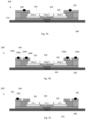
- FIGS. 6 A-C illustrate various example configurations for the sealing support structure in relation to the circuitry to be cooled by a direct cooling system sealed by the sealing support structure.
- FIG. 6 A provides an example sealing structure 140 configured as described above in connection with FIG. 1 A .
- the sealing support structure 140 extends around a periphery of the processing components.
- FIGS. 6 B and 6 C show examples where the sealing support structures are configured to form separate cooling zones.
- sealing support structure 240 surrounds each chip 101 - 105 separately.
- sealing support structure 340 also forms separate cooling zones, though fewer than in FIG. 6 B .
- the sealing support structure 340 surrounds the central chip 103 , and surrounds pairs of the peripheral chips 101 , 102 , 104 , 105 , rather than surrounding each chip separately as in FIG. 6 B .
- the configuration for the sealing support structure may be selected based on cooling needs, space for constructing the support structure, and other considerations. While a few example configurations are shown, it should be understood that any number of configuration are possible, and that the configurations may be adapted to various configurations of electronic components.
- FIGS. 7 A- 7 C are examples of various sealing support structures with one or more windows that can be applied to respective subassemblies 200 , 200 ′ and 200 ′′ of a direct liquid cooled module.
- Each of these figures is a cross-sectional front plan view as opposed to the top view of FIG. 1 A , for example. Therefore, while it looks like there are multiple groove bodies in FIG. 7 A for example, there is only one sealing support structure 240 that forms a closed perimeter as does the sealing support structure 140 of FIG. 1 A .
- Each of the respective subassemblies of FIGS. 7 A- 7 C includes chips 101 - 105 , a silicon interposer 210 , a substrate 215 , and a printed circuit board 225 .
- An epoxy 260 acts as a filler and support for the groove bodies 240 .
- FIG. 7 A there is a single sealing support structure 240 .
- An O-ring or gasket 150 sits in window 238 of sealing support structure 240 .
- Sealing support structure 240 wraps around a top portion of epoxy 260 such that a portion of sealing support structure 240 contacts both substrate 115 and chips 102 , 105 .
- FIG. 7 B there is an external window 238 a and an internal window 238 b in sealing support structure 240 .
- An aperture 244 between windows 238 a , 238 b allows epoxy 260 to be provided in an enclosure formed by windows 238 a , 238 b , chips 102 , 105 , silicon interposer 210 and substrate 215 .
- O-ring or gasket 150 a is received within window 238 a and O-ring or gasket 150 b is received within window 238 b.
- sealing support structure 240 there is only one window 238 in sealing support structure 240 , but there is still an aperture 244 adjacent window 238 and through sealing support structure 240 to allow epoxy to be received in an enclosure formed by sealing support structure 240 , chips 102 , 105 , silicon interposer 210 and substrate 215 .
- O-ring 150 or gasket is received within window 238 of sealing support structure 240 .
- FIGS. 8 A and 8 B are examples of respective sealing structures 300 ′, 300 ′′ added to subassembly 200 of FIG. 7 A .
- FIG. 8 A is the addition of jet impingement structure 300 ′
- FIG. 8 B is the addition of a manifold structure 300 ′′ for delivering coolant to the module or package.
- Both jet impingement structure 300 ′ and manifold structure 300 ′′ include a top plate 320 , in an inlet 330 and outlets 340 .
- O-ring or gasket 150 compresses which creates a hermetic seal between jet impingement structure 300 ′ and subassembly 200 .
- each arrow follows along a path that is generally parallel to longitudinal axis L 1 .
- liquid or gas enters into the module through inlet 330 and then through jets 332 onto the surface of chips 101 - 105 before travelling in a longitudinal direction L 2 perpendicular to axis L 1 and into return tubes 328 along axis L 1 again before being expelled from the module through outlets 340 .
- liquid or gas enters into the module through inlet 330 and then through flow channels 370 onto the surface of chips 101 - 105 before travelling in a longitudinal direction L 2 perpendicular to axis L 1 and into return tubes 328 along axis L 1 again before being expelled from the module through outlets 340 .
- Flow channels in a manifold are part of a direct liquid cooled module for directing liquid or gas to a chip (such as chips 101 - 105 ) that the manifold sits on top of.
- a manifold is designed to direct flow over one or more circuit components, such as microprocessors, memory chips, etc., in order to improve heat transfer between the components and the working fluid.
- a manifold is a component sitting on top of a chip with flow channels that creates a crossflow path for the coolant resulting in improved heat transfer between the chip and the working fluid or gas.
- the manifold is made of polyurethane. In other examples, manifold may be made of other polymers.
- FIGS. 9 A and 9 B are examples of loading an O-ring used in a direct liquid cooled module with different mechanical attachments.
- FIG. 9 A shows the use of a spring loaded screw 400 and bolster plate 500 in the direct liquid cooled module of FIG. 8 A .
- Bolster plate 500 is coupled to printed circuit board 225 .
- Screw 400 is inserted through an aperture in top plate 320 and both printed circuit board 225 and bolster plate 500 .
- a spring 420 is compressed between a head 410 of screw 400 and a top surface 336 of top plate 320 . This provides a top plate clamp load to O-ring 150 within window 238 of sealing support structure 240 .
- additional screw 400 ′ is used to provide an O-ring clamp load.
- Screw 400 ′ is inserted through another aperture in top plate 320 and is retained within sealing support structure 240 to apply a compressive loading on O-ring or gasket 150 .
- the sealing support structure 240 can be a stiffener that sealing support structure 240 is applied to such that screw 400 ′ is inserted through an aperture in top plate 320 and is retained within stiffener to apply a compressive load on O-ring or gasket 250 .
- Screws 400 and 400 ′ each have respective top portions 442 , 442 ′ and threaded shaft portions 444 , 444 ′.
- FIG. 9 A there are two screws 400 and in FIG. 9 B there are two screws 400 and two screws 400 ′.
- FIG. 10 A provides an example of a lid sealing structure, which may be used without an O-ring or gasket.
- lid 525 is configured to extend from a periphery of substrate 115 and form a seal between the chips 102 , 105 and the lid 525 , thereby preventing leakage of coolant 580 .
- the seal may be formed by adhesive 573 between the chips and the lid 525 .
- the lid 525 may be further secured to the substrate 115 by adhesive 572 .
- the adhesives 572 , 573 may be polymer-based, metal-based, or some combination thereof.
- the lid 525 can be made of any material, such as metal, polymer, or a combination of materials.
- a metallization layer 574 may be deposited on the chips 102 , 105 which contact the adhesive 573 or on a surface of the substrate 115 that contacts the adhesive 572 .
- Screws 400 may supply a compressive load to assist the adhesion provided by adhesives 572 , 573 .
- a compressive load may be provided by clamping or other mechanical forces.
- an epoxy 262 may be deposited between the chips 102 , 105 and the lid 525 , such that a portion of the lid 525 that extends from the substrate 115 wraps around the epoxy 262 .
- the epoxy 262 may provide support for the lid 525 .
- different shapes and configurations of lids may not require the epoxy.
- FIG. 10 B provides another example of a lid sealing structure.
- lid 625 is bonded to fins 690 of a coolant delivery structure via adhesive 672 .
- additional adhesive may be applied between the lid 625 and other components of the assembly to form a waterproof seal.
Landscapes
- Engineering & Computer Science (AREA)
- Theoretical Computer Science (AREA)
- Physics & Mathematics (AREA)
- General Physics & Mathematics (AREA)
- Human Computer Interaction (AREA)
- General Engineering & Computer Science (AREA)
- Power Engineering (AREA)
- Microelectronics & Electronic Packaging (AREA)
- Cooling Or The Like Of Semiconductors Or Solid State Devices (AREA)
- Condensed Matter Physics & Semiconductors (AREA)
- Computer Hardware Design (AREA)
Abstract
Description
Claims (16)
Priority Applications (1)
| Application Number | Priority Date | Filing Date | Title |
|---|---|---|---|
| US17/971,087 US12272619B2 (en) | 2020-05-21 | 2022-10-21 | Direct liquid cooling with O-ring sealing |
Applications Claiming Priority (2)
| Application Number | Priority Date | Filing Date | Title |
|---|---|---|---|
| US16/880,417 US11488890B2 (en) | 2020-05-21 | 2020-05-21 | Direct liquid cooling with O-ring sealing |
| US17/971,087 US12272619B2 (en) | 2020-05-21 | 2022-10-21 | Direct liquid cooling with O-ring sealing |
Related Parent Applications (1)
| Application Number | Title | Priority Date | Filing Date |
|---|---|---|---|
| US16/880,417 Continuation US11488890B2 (en) | 2020-05-21 | 2020-05-21 | Direct liquid cooling with O-ring sealing |
Publications (2)
| Publication Number | Publication Date |
|---|---|
| US20230037380A1 US20230037380A1 (en) | 2023-02-09 |
| US12272619B2 true US12272619B2 (en) | 2025-04-08 |
Family
ID=73726541
Family Applications (2)
| Application Number | Title | Priority Date | Filing Date |
|---|---|---|---|
| US16/880,417 Active 2040-05-22 US11488890B2 (en) | 2020-05-21 | 2020-05-21 | Direct liquid cooling with O-ring sealing |
| US17/971,087 Active US12272619B2 (en) | 2020-05-21 | 2022-10-21 | Direct liquid cooling with O-ring sealing |
Family Applications Before (1)
| Application Number | Title | Priority Date | Filing Date |
|---|---|---|---|
| US16/880,417 Active 2040-05-22 US11488890B2 (en) | 2020-05-21 | 2020-05-21 | Direct liquid cooling with O-ring sealing |
Country Status (4)
| Country | Link |
|---|---|
| US (2) | US11488890B2 (en) |
| EP (1) | EP3913666A1 (en) |
| CN (1) | CN112216663A (en) |
| TW (2) | TWI836155B (en) |
Families Citing this family (6)
| Publication number | Priority date | Publication date | Assignee | Title |
|---|---|---|---|---|
| CN210467924U (en) * | 2019-09-17 | 2020-05-05 | 宁德时代新能源科技股份有限公司 | A battery pack and vehicle |
| DK3926669T3 (en) | 2020-05-29 | 2025-02-10 | Google Llc | METHODS AND HEAT DISTRIBUTION DEVICES FOR THERMAL MANAGEMENT OF CHIP ASSEMBLIES |
| CN117280464A (en) * | 2021-06-04 | 2023-12-22 | 华为技术有限公司 | Liquid-cooled chip packaging structure, printed circuit board assembly and method, electronic device |
| CN115274569A (en) * | 2022-06-23 | 2022-11-01 | 超聚变数字技术有限公司 | Electronic device and server |
| CN118841379A (en) * | 2023-04-25 | 2024-10-25 | 华为技术有限公司 | Chip packaging structure and electronic equipment |
| WO2026032723A1 (en) * | 2024-08-06 | 2026-02-12 | Corintis Sa | Semiconductor device with improved cooling as well as components and methods for achieving same |
Citations (20)
| Publication number | Priority date | Publication date | Assignee | Title |
|---|---|---|---|---|
| US5349831A (en) | 1991-11-08 | 1994-09-27 | Hitachi, Ltd. | Apparatus for cooling heat generating members |
| US6351384B1 (en) * | 1999-08-11 | 2002-02-26 | Hitachi, Ltd. | Device and method for cooling multi-chip modules |
| US20030178176A1 (en) * | 2002-03-22 | 2003-09-25 | Jenkins Kurt A. | System and method for providing cooling systems with heat exchangers |
| JP2005032904A (en) | 2003-07-10 | 2005-02-03 | Hitachi Ltd | Direct liquid-cooled power semiconductor module |
| US20060183328A1 (en) | 1999-05-17 | 2006-08-17 | Barstad Leon R | Electrolytic copper plating solutions |
| JP2007250918A (en) | 2006-03-17 | 2007-09-27 | Mitsubishi Electric Corp | Directly cooled power semiconductor device |
| US20080284047A1 (en) | 2007-05-15 | 2008-11-20 | Eric Tosaya | Chip Package with Stiffener Ring |
| CN101345223A (en) | 2007-06-06 | 2009-01-14 | 通用汽车环球科技运作公司 | Semiconductor device, semiconductor module and method for cooling semiconductor device |
| US8536711B2 (en) | 2007-03-30 | 2013-09-17 | Elpida Memory, Inc. | Chip-stacked semiconductor and manufacturing method thereof |
| US20130329460A1 (en) * | 2012-06-08 | 2013-12-12 | Apple Inc. | Electronic Device Display Structures |
| JP2014192409A (en) | 2013-03-28 | 2014-10-06 | Fujitsu Ltd | Micro channel heat exchange device and electronic equipment |
| WO2014171276A1 (en) | 2013-04-16 | 2014-10-23 | 日産自動車株式会社 | Cooling device for heat-generating element |
| US8946889B2 (en) | 2010-06-23 | 2015-02-03 | Denso Corporation | Semiconductor module with cooling mechanism and production method thereof |
| US9564385B2 (en) | 2015-04-30 | 2017-02-07 | Deere & Company | Package for a semiconductor device |
| US20170196120A1 (en) | 2015-12-30 | 2017-07-06 | Imec Vzw | Liquid cooling of electronic devices |
| US20180076113A1 (en) | 2016-09-15 | 2018-03-15 | International Business Machines Corporation | Chip package for two-phase cooling and assembly process thereof |
| US20180211900A1 (en) | 2017-01-26 | 2018-07-26 | Intel Corporation | Techniques For Fluid Cooling Of Integrated Circuits In Packages |
| US20190327859A1 (en) | 2018-04-19 | 2019-10-24 | Google Llc | Cooling electronic devices in a data center |
| US10548240B1 (en) | 2019-01-11 | 2020-01-28 | Google Llc | Cooling electronic devices in a data center |
| US10561040B1 (en) | 2018-10-08 | 2020-02-11 | Hewlett Packard Enterprise Development Lp | Flexible gasket seal for direct liquid cooling of electronic devices |
-
2020
- 2020-05-21 US US16/880,417 patent/US11488890B2/en active Active
- 2020-10-21 CN CN202011131022.3A patent/CN112216663A/en active Pending
- 2020-11-05 TW TW109138668A patent/TWI836155B/en active
- 2020-11-05 TW TW113105668A patent/TWI874136B/en active
- 2020-12-01 EP EP20211019.3A patent/EP3913666A1/en active Pending
-
2022
- 2022-10-21 US US17/971,087 patent/US12272619B2/en active Active
Patent Citations (23)
| Publication number | Priority date | Publication date | Assignee | Title |
|---|---|---|---|---|
| US5349831A (en) | 1991-11-08 | 1994-09-27 | Hitachi, Ltd. | Apparatus for cooling heat generating members |
| US20060183328A1 (en) | 1999-05-17 | 2006-08-17 | Barstad Leon R | Electrolytic copper plating solutions |
| US6351384B1 (en) * | 1999-08-11 | 2002-02-26 | Hitachi, Ltd. | Device and method for cooling multi-chip modules |
| US20030178176A1 (en) * | 2002-03-22 | 2003-09-25 | Jenkins Kurt A. | System and method for providing cooling systems with heat exchangers |
| JP2005032904A (en) | 2003-07-10 | 2005-02-03 | Hitachi Ltd | Direct liquid-cooled power semiconductor module |
| JP2007250918A (en) | 2006-03-17 | 2007-09-27 | Mitsubishi Electric Corp | Directly cooled power semiconductor device |
| US8536711B2 (en) | 2007-03-30 | 2013-09-17 | Elpida Memory, Inc. | Chip-stacked semiconductor and manufacturing method thereof |
| US20080284047A1 (en) | 2007-05-15 | 2008-11-20 | Eric Tosaya | Chip Package with Stiffener Ring |
| CN101345223A (en) | 2007-06-06 | 2009-01-14 | 通用汽车环球科技运作公司 | Semiconductor device, semiconductor module and method for cooling semiconductor device |
| US8946889B2 (en) | 2010-06-23 | 2015-02-03 | Denso Corporation | Semiconductor module with cooling mechanism and production method thereof |
| US20130329460A1 (en) * | 2012-06-08 | 2013-12-12 | Apple Inc. | Electronic Device Display Structures |
| JP2014192409A (en) | 2013-03-28 | 2014-10-06 | Fujitsu Ltd | Micro channel heat exchange device and electronic equipment |
| WO2014171276A1 (en) | 2013-04-16 | 2014-10-23 | 日産自動車株式会社 | Cooling device for heat-generating element |
| CN105144375A (en) | 2013-04-16 | 2015-12-09 | 日产自动车株式会社 | Cooling device for heat-generating element |
| EP2988329A1 (en) | 2013-04-16 | 2016-02-24 | Nissan Motor Co., Ltd. | Cooling device for heat-generating element |
| US20160064303A1 (en) | 2013-04-16 | 2016-03-03 | Nissan Motor Co., Ltd. | Cooling apparatus for a heat-generating element |
| US9564385B2 (en) | 2015-04-30 | 2017-02-07 | Deere & Company | Package for a semiconductor device |
| US20170196120A1 (en) | 2015-12-30 | 2017-07-06 | Imec Vzw | Liquid cooling of electronic devices |
| US20180076113A1 (en) | 2016-09-15 | 2018-03-15 | International Business Machines Corporation | Chip package for two-phase cooling and assembly process thereof |
| US20180211900A1 (en) | 2017-01-26 | 2018-07-26 | Intel Corporation | Techniques For Fluid Cooling Of Integrated Circuits In Packages |
| US20190327859A1 (en) | 2018-04-19 | 2019-10-24 | Google Llc | Cooling electronic devices in a data center |
| US10561040B1 (en) | 2018-10-08 | 2020-02-11 | Hewlett Packard Enterprise Development Lp | Flexible gasket seal for direct liquid cooling of electronic devices |
| US10548240B1 (en) | 2019-01-11 | 2020-01-28 | Google Llc | Cooling electronic devices in a data center |
Non-Patent Citations (10)
| Title |
|---|
| Decision of Rejection for Chinese Patent Application No. 202011131022.3, dated May 8, 2024. 5 pages. |
| Extended European Search Report for European Patent Application No. 20211019.3 dated Sep. 15, 2021. 13 pages. |
| Nelson et al. Thermal Performance of an Integral Immersion Cooled Multichip Module Package, IEEE Transactions on Components, Packaging and Manufacturing Technology: Part A, IEEE Service Center, Piscataway, NJ, US, vol. 17, No. 3, Sep. 1, 1994 (Sep. 1, 1994), pp. 405-412. |
| Office Action for Chinese Patent Application No. 202011131022.3 dated Sep. 7, 2023. 8 pages. |
| Office Action for European Patent Application No. 20211019.3 dated Nov. 20, 2023. 8 pages. |
| Office Action for European Patent Application No. 20211019.3 dated Nov. 20, 2024. 8 pages. |
| Office Action for Taiwanese Patent Application No. 109138668 dated Jul. 27, 2023. 10 pages. |
| Office Action for Taiwanese Patent Application No. 113105668 dated Jul. 15, 2024. 8 pages. |
| Partial European Search Report for European Patent Application No. 20211019.3 dated Jun. 15, 2021. 14 pages. |
| Second Office Action for Chinese Patent Application No. 202011131022.3 dated Feb. 3, 2024. 6 pages. |
Also Published As
| Publication number | Publication date |
|---|---|
| CN112216663A (en) | 2021-01-12 |
| US20230037380A1 (en) | 2023-02-09 |
| TW202422815A (en) | 2024-06-01 |
| TWI874136B (en) | 2025-02-21 |
| EP3913666A1 (en) | 2021-11-24 |
| TW202145473A (en) | 2021-12-01 |
| US20210366807A1 (en) | 2021-11-25 |
| TWI836155B (en) | 2024-03-21 |
| US11488890B2 (en) | 2022-11-01 |
Similar Documents
| Publication | Publication Date | Title |
|---|---|---|
| US12272619B2 (en) | Direct liquid cooling with O-ring sealing | |
| US11310937B2 (en) | Impinging jet manifold for chip cooling near edge jets | |
| JP5414349B2 (en) | Electronic equipment | |
| US6154369A (en) | Electronic assembly for removing heat from a semiconductor device | |
| US12315782B2 (en) | Spring loaded compliant coolant distribution manifold for direct liquid cooled modules | |
| US20040057214A1 (en) | Thermally enhanced lid for multichip modules | |
| US11658091B2 (en) | Methods of manufacturing semiconductor packaging device and heat dissipation structure | |
| HK40044423A (en) | Direct liquid cooling with o-ring sealing | |
| US20230260931A1 (en) | Weight Optimized Stiffener and Sealing Structure for Direct Liquid Cooled Modules | |
| HK40041906B (en) | Spring loaded compliant coolant distribution manifold for direct liquid cooled modules | |
| HK40041906A (en) | Spring loaded compliant coolant distribution manifold for direct liquid cooled modules | |
| HK40044576A (en) | Weight optimized stiffener and sealing structure for direct liquid cooled modules | |
| HK40044576B (en) | Weight optimized stiffener and sealing structure for direct liquid cooled modules | |
| HK40044422A (en) | Impinging jet manifold for chip cooling near edge jets |
Legal Events
| Date | Code | Title | Description |
|---|---|---|---|
| FEPP | Fee payment procedure |
Free format text: ENTITY STATUS SET TO UNDISCOUNTED (ORIGINAL EVENT CODE: BIG.); ENTITY STATUS OF PATENT OWNER: LARGE ENTITY |
|
| AS | Assignment |
Owner name: GOOGLE LLC, CALIFORNIA Free format text: ASSIGNMENT OF ASSIGNORS INTEREST;ASSIGNORS:PADILLA, JORGE;IYENGAR, MADHUSUDAN K.;BURGESS, CONNOR;AND OTHERS;SIGNING DATES FROM 20200520 TO 20200722;REEL/FRAME:061543/0371 |
|
| STPP | Information on status: patent application and granting procedure in general |
Free format text: DOCKETED NEW CASE - READY FOR EXAMINATION |
|
| STPP | Information on status: patent application and granting procedure in general |
Free format text: NON FINAL ACTION MAILED |
|
| STPP | Information on status: patent application and granting procedure in general |
Free format text: RESPONSE TO NON-FINAL OFFICE ACTION ENTERED AND FORWARDED TO EXAMINER |
|
| STPP | Information on status: patent application and granting procedure in general |
Free format text: FINAL REJECTION MAILED |
|
| STPP | Information on status: patent application and granting procedure in general |
Free format text: RESPONSE AFTER FINAL ACTION FORWARDED TO EXAMINER |
|
| STPP | Information on status: patent application and granting procedure in general |
Free format text: ADVISORY ACTION MAILED |
|
| STPP | Information on status: patent application and granting procedure in general |
Free format text: RESPONSE AFTER FINAL ACTION FORWARDED TO EXAMINER |
|
| STPP | Information on status: patent application and granting procedure in general |
Free format text: ADVISORY ACTION MAILED |
|
| STPP | Information on status: patent application and granting procedure in general |
Free format text: DOCKETED NEW CASE - READY FOR EXAMINATION |
|
| STPP | Information on status: patent application and granting procedure in general |
Free format text: NOTICE OF ALLOWANCE MAILED -- APPLICATION RECEIVED IN OFFICE OF PUBLICATIONS |
|
| ZAAB | Notice of allowance mailed |
Free format text: ORIGINAL CODE: MN/=. |
|
| STPP | Information on status: patent application and granting procedure in general |
Free format text: AWAITING TC RESP., ISSUE FEE NOT PAID |
|
| STPP | Information on status: patent application and granting procedure in general |
Free format text: NOTICE OF ALLOWANCE MAILED -- APPLICATION RECEIVED IN OFFICE OF PUBLICATIONS |
|
| STPP | Information on status: patent application and granting procedure in general |
Free format text: PUBLICATIONS -- ISSUE FEE PAYMENT VERIFIED |
|
| STPP | Information on status: patent application and granting procedure in general |
Free format text: PUBLICATIONS -- ISSUE FEE PAYMENT VERIFIED |
|
| STCF | Information on status: patent grant |
Free format text: PATENTED CASE |