US12272292B2 - Method and system for controlling voltage output, display device, electronic device, and non-transitory computer readable medium - Google Patents
Method and system for controlling voltage output, display device, electronic device, and non-transitory computer readable medium Download PDFInfo
- Publication number
- US12272292B2 US12272292B2 US18/576,354 US202318576354A US12272292B2 US 12272292 B2 US12272292 B2 US 12272292B2 US 202318576354 A US202318576354 A US 202318576354A US 12272292 B2 US12272292 B2 US 12272292B2
- Authority
- US
- United States
- Prior art keywords
- picture
- displayed
- sub
- power supply
- supply module
- Prior art date
- Legal status (The legal status is an assumption and is not a legal conclusion. Google has not performed a legal analysis and makes no representation as to the accuracy of the status listed.)
- Active
Links
Images


Classifications
-
- G—PHYSICS
- G09—EDUCATION; CRYPTOGRAPHY; DISPLAY; ADVERTISING; SEALS
- G09G—ARRANGEMENTS OR CIRCUITS FOR CONTROL OF INDICATING DEVICES USING STATIC MEANS TO PRESENT VARIABLE INFORMATION
- G09G3/00—Control arrangements or circuits, of interest only in connection with visual indicators other than cathode-ray tubes
- G09G3/20—Control arrangements or circuits, of interest only in connection with visual indicators other than cathode-ray tubes for presentation of an assembly of a number of characters, e.g. a page, by composing the assembly by combination of individual elements arranged in a matrix no fixed position being assigned to or needed to be assigned to the individual characters or partial characters
- G09G3/34—Control arrangements or circuits, of interest only in connection with visual indicators other than cathode-ray tubes for presentation of an assembly of a number of characters, e.g. a page, by composing the assembly by combination of individual elements arranged in a matrix no fixed position being assigned to or needed to be assigned to the individual characters or partial characters by control of light from an independent source
- G09G3/36—Control arrangements or circuits, of interest only in connection with visual indicators other than cathode-ray tubes for presentation of an assembly of a number of characters, e.g. a page, by composing the assembly by combination of individual elements arranged in a matrix no fixed position being assigned to or needed to be assigned to the individual characters or partial characters by control of light from an independent source using liquid crystals
-
- G—PHYSICS
- G09—EDUCATION; CRYPTOGRAPHY; DISPLAY; ADVERTISING; SEALS
- G09G—ARRANGEMENTS OR CIRCUITS FOR CONTROL OF INDICATING DEVICES USING STATIC MEANS TO PRESENT VARIABLE INFORMATION
- G09G3/00—Control arrangements or circuits, of interest only in connection with visual indicators other than cathode-ray tubes
- G09G3/20—Control arrangements or circuits, of interest only in connection with visual indicators other than cathode-ray tubes for presentation of an assembly of a number of characters, e.g. a page, by composing the assembly by combination of individual elements arranged in a matrix no fixed position being assigned to or needed to be assigned to the individual characters or partial characters
- G09G3/2092—Details of a display terminals using a flat panel, the details relating to the control arrangement of the display terminal and to the interfaces thereto
-
- G—PHYSICS
- G09—EDUCATION; CRYPTOGRAPHY; DISPLAY; ADVERTISING; SEALS
- G09G—ARRANGEMENTS OR CIRCUITS FOR CONTROL OF INDICATING DEVICES USING STATIC MEANS TO PRESENT VARIABLE INFORMATION
- G09G3/00—Control arrangements or circuits, of interest only in connection with visual indicators other than cathode-ray tubes
- G09G3/20—Control arrangements or circuits, of interest only in connection with visual indicators other than cathode-ray tubes for presentation of an assembly of a number of characters, e.g. a page, by composing the assembly by combination of individual elements arranged in a matrix no fixed position being assigned to or needed to be assigned to the individual characters or partial characters
- G09G3/22—Control arrangements or circuits, of interest only in connection with visual indicators other than cathode-ray tubes for presentation of an assembly of a number of characters, e.g. a page, by composing the assembly by combination of individual elements arranged in a matrix no fixed position being assigned to or needed to be assigned to the individual characters or partial characters using controlled light sources
- G09G3/30—Control arrangements or circuits, of interest only in connection with visual indicators other than cathode-ray tubes for presentation of an assembly of a number of characters, e.g. a page, by composing the assembly by combination of individual elements arranged in a matrix no fixed position being assigned to or needed to be assigned to the individual characters or partial characters using controlled light sources using electroluminescent panels
- G09G3/32—Control arrangements or circuits, of interest only in connection with visual indicators other than cathode-ray tubes for presentation of an assembly of a number of characters, e.g. a page, by composing the assembly by combination of individual elements arranged in a matrix no fixed position being assigned to or needed to be assigned to the individual characters or partial characters using controlled light sources using electroluminescent panels semiconductive, e.g. using light-emitting diodes [LED]
- G09G3/3208—Control arrangements or circuits, of interest only in connection with visual indicators other than cathode-ray tubes for presentation of an assembly of a number of characters, e.g. a page, by composing the assembly by combination of individual elements arranged in a matrix no fixed position being assigned to or needed to be assigned to the individual characters or partial characters using controlled light sources using electroluminescent panels semiconductive, e.g. using light-emitting diodes [LED] organic, e.g. using organic light-emitting diodes [OLED]
-
- G—PHYSICS
- G09—EDUCATION; CRYPTOGRAPHY; DISPLAY; ADVERTISING; SEALS
- G09G—ARRANGEMENTS OR CIRCUITS FOR CONTROL OF INDICATING DEVICES USING STATIC MEANS TO PRESENT VARIABLE INFORMATION
- G09G2310/00—Command of the display device
- G09G2310/08—Details of timing specific for flat panels, other than clock recovery
-
- G—PHYSICS
- G09—EDUCATION; CRYPTOGRAPHY; DISPLAY; ADVERTISING; SEALS
- G09G—ARRANGEMENTS OR CIRCUITS FOR CONTROL OF INDICATING DEVICES USING STATIC MEANS TO PRESENT VARIABLE INFORMATION
- G09G2320/00—Control of display operating conditions
- G09G2320/02—Improving the quality of display appearance
- G09G2320/0233—Improving the luminance or brightness uniformity across the screen
-
- G—PHYSICS
- G09—EDUCATION; CRYPTOGRAPHY; DISPLAY; ADVERTISING; SEALS
- G09G—ARRANGEMENTS OR CIRCUITS FOR CONTROL OF INDICATING DEVICES USING STATIC MEANS TO PRESENT VARIABLE INFORMATION
- G09G2330/00—Aspects of power supply; Aspects of display protection and defect management
- G09G2330/02—Details of power systems and of start or stop of display operation
- G09G2330/028—Generation of voltages supplied to electrode drivers in a matrix display other than LCD
Definitions
- the present disclosure relates to the display field, in particular, relates to a method and system for controlling voltage output, a display control system, a display device, an electronic device, and a non-transitory computer-readable medium.
- a display device generally includes a display control system and a display panel (including source driver circuits and gate driver circuits).
- the display control system includes a power supply module, with its core component being the charge pump, also referred to as a booster circuit.
- the power supply module is configured to provide the required operating voltage to the display panel, which includes but is not limited to high-level operating voltage VGH, low-level operating voltage VGL, reference voltage Vref, initialization voltage Vinit, common voltage Vcom, etc.
- the power supply module provides operating voltage to the display panel at a preset operating frequency (also referred to as the output frequency of the power supply module).
- the operating frequency of the current power supply module is set based on considerations about the power consumption of the power supply module. In practical applications, it has been observed that the current power supply module, during the process of outputting operating voltage to the display panel, has a certain impact on the display frame, leading to the appearance of noticeable unevenness (mura) in the display frame.
- the present disclosure provides a method and system for controlling voltage output, a display control system, a display device, an electronic device, and a non-transitory computer-readable medium.
- a method for controlling voltage output is provided according to the embodiments disclosed herein.
- the method is used to control a power supply module to provide a required operating voltage to a display panel, and a process of displaying a frame on the display panel includes a plurality of sequential row driving periods, each row driving period including a charging period and a non-charging period, wherein during the charging period, a connection between a data line and a corresponding row of sub-pixels is enabled so that data voltages are written into the corresponding sub-pixels; and during the non-charging period, the data line is disconnected from the sub-pixels;
- the method further includes: detecting whether the picture to be displayed is a first picture,
- the first picture is an overloading picture.
- the method further includes:
- the step of controlling the power supply module to output the operating voltage at the preset first operating frequency during the display of the picture to be displayed includes:
- the display panel includes a plurality of columns of sub-pixels, each column of sub-pixels being configured with a corresponding data line, wherein the sub-pixels disposed at a same column are all connected to the corresponding data line;
- the display panel includes M*N sub-pixels arranged in an array with N rows and M columns;
- the first operating frequency f1 satisfies:
- a system for controlling voltage output is further provided according to the embodiments disclosed herein.
- the system is configured to control a power supply module to provide a required operating voltage to a display panel, and a process of displaying a frame on the display panel includes a plurality of sequential row driving periods, each row driving period including a charging period and a non-charging period, wherein during the charging period, a connection between a data line and a corresponding row of sub-pixels is enabled so that data voltages are written into the corresponding sub-pixels; and during the non-charging period, the data line is disconnected from the sub-pixels;
- system further includes:
- the first picture is an overloading picture.
- system further includes:
- the first control module specifically includes:
- the display panel includes a plurality of columns of sub-pixels, each column of sub-pixels being configured with a corresponding data line, wherein the sub-pixels disposed at a same column are all connected to the corresponding data line;
- the display panel includes M*N sub-pixels arranged in an array with N rows and M columns;
- the first operating frequency f1 satisfies:
- a display control system is further provided according to the embodiments disclosed herein.
- the system includes a power supply module and the system for controlling voltage output provided according to the second aspect.
- a display device is further provided according to the embodiments disclosed herein.
- the display device includes a display panel and the display control system provided according to the third aspect.
- an electronic device is further provided according to the embodiments disclosed herein.
- the electronic device includes:
- the processor includes a field-programmable gate array.
- a non-transitory computer-readable medium is further provided according to the embodiments disclosed herein.
- the non-transitory computer-readable medium stores a computer program, wherein the computer program, when running on a processor, causes the processor to implement the steps in the method for controlling voltage output provided according to the first aspect.
- FIG. 1 is a block diagram of a systematic structure of a display device according to the technical solutions of the present disclosure
- FIG. 2 is a schematic diagram of a circuit structure of a sub-pixel according to some embodiments of the present disclosure
- FIG. 3 is a schematic diagram of another circuit structure of a sub-pixel according to some embodiments of the present disclosure.
- FIG. 4 is a schematic diagram of the circuit structure of a power supply module according to some embodiments of the present disclosure.
- FIG. 5 is a timing diagram of the voltage Vpph to be outputted inside a power supply module
- FIG. 6 is a time distribution diagram of displaying a frame according to some embodiments of the present disclosure.
- FIG. 7 is a timing diagram of the voltage Vpph to be outputted inside a power supply module and the display of a frame according to the related art
- FIG. 8 is a flowchart of a method for controlling voltage output according to some embodiments of the present disclosure.
- FIG. 9 a is a flowchart of another method for controlling voltage output according to some embodiments of the present disclosure.
- FIG. 9 b is a flowchart of still another method for controlling voltage output according to some embodiments of the present disclosure.
- FIG. 10 is a timing diagram of the voltage Vpph to be outputted inside a power supply module and the display of a frame according to the present disclosure
- FIG. 11 is a flowchart of an optional implementation of step S 1 according to some embodiments of the present disclosure.
- FIG. 12 is a structural block diagram of a system for controlling voltage output according to some embodiments of the present disclosure.
- FIG. 13 is a schematic structural diagram of an electronic device according to some embodiments of the present disclosure.
- FIG. 1 is a block diagram of a systematic structure of a display device according to the technical solutions of the present disclosure. As illustrated, FIG. 1 includes a display panel 1 and a display control system 2 .
- the display panel 1 can be categorized, based on the display dimension, as a 2D or 3D display panel. Additionally, the display panel 1 can be categorized, based on the type of illumination, as a liquid crystal display panel (LCD), a light-emitting diode (LED) display panel, an organic light-emitting diode (OLED) display panel, or a quantum dot light-emitting diode (QLED) display panel.
- LCD liquid crystal display panel
- LED light-emitting diode
- OLED organic light-emitting diode
- QLED quantum dot light-emitting diode
- the display panel includes a plurality of sub-pixels arranged in an array along the row and column directions, each sub-pixel being connected to a corresponding row gate line and a corresponding column data line, wherein the sub-pixels disposed at the same row are connected to the same gate line, and the sub-pixels disposed at the same column are connected to the same data line.
- the display panel 1 is configured with a gate driver circuit (not shown) and a source driver circuit (not shown).
- the gate driver circuit is configured to provide gate drive signals to the gate lines, enabling scanning and driving of the gate lines.
- the source driver circuit is configured to provide data voltage to the data lines, writing the data voltage through the data lines into the corresponding sub-pixels to control the grayscale display.
- FIG. 2 is a schematic diagram of a circuit structure of a sub-pixel according to some embodiments of the present disclosure.
- the sub-pixel is part of the liquid crystal display panel 1 and includes a switch transistor T 0 and a pixel electrode.
- the control electrode of the switch transistor T 0 is connected to the corresponding row gate line GATE, the first electrode of the switch transistor T 0 is connected to the data line DATA, and the second electrode of the switch transistor T 0 is connected to the pixel electrode.
- the switch transistor T 0 conducts, allowing the data voltage from the data line DATA to be written into the pixel electrode.
- FIG. 3 is a schematic diagram of another circuit structure of a sub-pixel according to some embodiments of the present disclosure.
- the sub-pixel is part of the LED/OLED/QLED display panel 1 and includes a data writing transistor T 1 , a driver transistor DTFT, and a light-emitting element EL (specifically LED, OLED, or QLED).
- the control electrode of the data writing transistor T 1 is connected to the corresponding row gate line GATE, the first electrode of the data writing transistor T 1 is connected to the data line DATA, and the second electrode of the data writing transistor T 1 is connected to the control electrode of the driver transistor DTFT.
- the first electrode of the driver transistor DTFT is connected to the power supply terminal VDD, and the second electrode of the driver transistor DTFT is connected to the light-emitting element EL.
- the drive signal provided by the gate line GATE is in an active level state
- the data writing transistor T 1 conducts, allowing the data voltage from the data line DATA to be written into the control electrode of the driver transistor DTFT.
- the driver transistor DTFT then outputs the corresponding driving current.
- circuit structure of the sub-pixel according to the embodiments disclosed herein is not limited to what is illustrated in FIGS. 2 and 3 ; other circuit structures can also be used, which are not individually exemplified here.
- the specific form of the gate driver circuit is a chip with gate driving functionality (commonly referred to as Gate IC), or it is a circuit structure formed directly in the peripheral area of the display panel based on array substrate technology (Gate on Array, abbreviated as GOA).
- the specific form of the source driver circuit is a chip with source driving functionality (commonly referred to as Source IC).
- Source IC is bonded to connection pads on the display panel through a flexible printed circuit (FPC).
- FPC flexible printed circuit
- the display control system 2 includes a system for controlling voltage output 3 and a power supply module 4 .
- the system for controlling voltage output 3 is configured to receive display data for the picture to be displayed (including data voltages for each sub-pixel) and control the power supply module 4 to operate.
- FIG. 4 is a schematic diagram of the circuit structure of a power supply module according to some embodiments of the present disclosure
- FIG. 5 is a timing diagram of the voltage Vpph to be outputted inside a power supply module.
- the core component of the power supply module 4 is a charge pump, which includes a booster circuit 401 and a voltage clamping circuit 402 .
- the booster circuit 401 performs boosting operations in response to the control of a clock signal CLK to gradually raise the voltage Vpph to be outputted.
- the enable signal pump_en of the booster circuit 401 transitions from a high level to a low level. Consequently, the booster circuit 401 is turned off, and the charge pump outputs the voltage Vpph as the operating voltage (with a relatively short output duration), thereby supplying power from the power supply module 4 to the display panel. Subsequently, when the voltage Vpph to be outputted decreases below the low clamping voltage of the voltage clamping circuit 402 due to discharge or other reasons, the enable signal pump_en of the booster circuit 401 transitions from a low level to a high level, restarting the booster circuit 401 . This cyclic process maintains the actual operating voltage outputted by the charge pump at a stable high level.
- booster circuits 401 and corresponding multiple voltage clamping circuits 402 are configured within the power supply module 4 .
- Each booster circuit 401 and its corresponding voltage clamping circuit 402 are configured to achieve the output of an operating voltage.
- the present disclosure does not impose restrictions on the specific circuit structure of the power supply module 4 .
- FIG. 6 is a time distribution diagram of displaying a frame according to some embodiments of the present disclosure.
- the process of displaying a frame on the display panel includes the pixel driving stage.
- the pixel driving stage includes a plurality of row driving periods p 0 , each corresponding to individual sub-pixel rows (only 9 row driving periods p 0 are illustratively depicted in FIG. 6 ).
- the plurality of row driving periods p 0 proceed sequentially, wherein each row driving period p 0 includes a charging period s 2 and a non-charging period s 1 .
- each row driving period are controlled by the horizontal synchronization signal HSYNC.
- the horizontal synchronization signal HSYNC transitions from a low level to a high level, it signifies the end of the previous row driving period p 0 and the start of the current row driving period p 0 .
- the gate driver circuit provides an active level signal, enabling the transistors for data writing (e.g., the switch transistor T 0 in FIG. 2 or the data writing transistor T 1 in FIG. 3 ) within the row of sub-pixels to be in a conducting state.
- the respective data lines write the corresponding data voltages Vd into each sub-pixel in the row of sub-pixels (commonly also referred to as the data voltage charging writing process).
- the non-charging period s 1 corresponding to the row of sub-pixels the data lines are disconnected from the sub-pixels.
- a non-charging period s 1 (commonly also referred to as a charging preparation period) is configured between the start of the row driving period p 0 and the start of the charging period s 2 .
- This charging preparation period within the current row driving period serves as a row buffer period between the charging period s 2 of the current row driving period and the charging period s 2 of the previous row driving period.
- a non-charging period s 1 configured between the start of the row driving period p 0 and the start of the charging period
- a non-charging period (commonly also referred to as a charging end stabilization period) is configured between the end of the charging period and the end of the row driving period.
- the charging preparation period within the current row driving period p 0 and the charging end stabilization period within the previous row driving period together serve as a row buffer period between the charging period s 2 within the current row driving period and the charging period s 2 within the previous row driving period. This scenario is not depicted in the accompanying drawings.
- G(n+1) to G(n+9) represent the (n+1)th to (n+9)th gate lines, respectively. That is, FIG. 6 illustrates the timing of the (n+1)th to (n+9)th row driving periods p 0 within the row driving periods p 0 .
- Vd_(n+1) to Vd_(n+9) in FIG. 6 represent the data voltages provided by a data line Data to the sub-pixels disposed in the (n+1)th to (n+9)th rows, respectively, wherein n represents a non-negative integer.
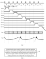
- FIG. 7 is a timing diagram of the voltage Vpph to be outputted inside a power supply module and the display of a frame according to the related art.
- the design of the operating frequency of the power supply module in the related art considers only the power consumption factors. Generally, the operating frequency is configured as low as possible while meeting the requirements of resistive-capacitive delay and power supply to achieve power reduction objectives.
- the times when the power supply module outputs the operating voltage according to the related art fall within the charging periods of some row driving periods, and their corresponding positions within the different charging periods vary.
- the time t 1 when the power supply module outputs the operating voltage falls within a position toward the end of the charging period within the (n+4)th row driving period
- the time t 2 when the power supply module outputs the operating voltage falls within a position toward the middle of the charging period within the (n+8)th row driving period.
- the times when the power supply module outputs the operating voltage vary in their positions within the row driving periods. For example, when displaying the current frame, the times when the power supply module outputs the operating voltage, as shown in FIG. 7 , fall within the (n+4)th and (n+8)th row driving periods. However, when displaying the next frame, the times when the power supply module outputs the operating voltage may fall within the (n+3)th and (n+7)th row driving periods (not shown in a corresponding figure).
- the power supply module while outputting operating voltage to the display panel, causes some interference in the process of writing data voltages from the data lines to the sub-pixels. Especially in the case that significant voltage changes are required on the data lines (i.e., when two pixel units in the same column and adjacent rows have notably different data voltage loads, putting the data line into an overloaded state), the interference caused by the display panel for outputting operating voltage to charge the sub-pixels amplifies. This results in an inability to accurately write data voltages into the sub-pixels, leading to abnormal sub-pixel display and ultimately causing mura in the display panel.
- FIG. 8 is a flowchart of a method for controlling voltage output according to some embodiments of the present disclosure.
- the method for controlling voltage output is employed within a system for controlling voltage output.
- the method for controlling voltage output is used to control the power supply module to provide the required operating voltage to the display panel.
- the process of displaying a frame on the display panel includes a plurality of sequential row driving periods, each row driving period including a charging period and a non-charging period, wherein during the charging period, the connection between the data line and the corresponding row of sub-pixels is enabled so that data voltages are written into the corresponding sub-pixels, and during the non-charging period, the data line is disconnected from the sub-pixels.
- the method for controlling voltage output includes:
- step S 2 the power supply module is controlled to output the operating voltage at a preset first operating frequency during the display of the picture to be displayed. Additionally, the time period during which the power supply module outputs the operating voltage to the display panel does not overlap with the charging period.
- the operating frequency of the power supply module is controlled to ensure that the time when the power supply module outputs operating voltage to the display panel does not fall within a charging period.
- the time when the power supply module outputs operating voltage (a very brief period) is staggered from the charging period of the sub-pixels.
- FIG. 9 a is a flowchart of another method for controlling voltage output according to some embodiments of the present disclosure. As illustrated in FIG. 9 a , the method for controlling voltage output includes:
- step S 1 a picture to be displayed is detected to determine whether it is a first picture.
- step S 2 Upon detecting that the picture to be displayed is a first picture in step S 1 , the following step S 2 is performed.
- step S 2 the power supply module is controlled to output the operating voltage at a preset first operating frequency during the display of the picture to be displayed. Additionally, the time period during which the power supply module outputs the operating voltage to the display panel does not overlap with the charging period.
- the first picture is an overloading picture.
- the overloading picture refers to a frame where there is a higher frequency and/or greater magnitude of data voltage variations among different sub-pixels within each column of the sub-pixels. It reflects a higher frequency and greater magnitude of data voltage variations on the same signal channel outputted by the source driver chip during the display. This leads to increased complexity in outputting data by the source driver chip, placing it in a high-load state.
- the picture to be displayed is initially detected to determine whether it is an overloading picture.
- the operating frequency of the power supply module is controlled to ensure that the time when the power supply module outputs operating voltage to the display panel does not fall within a charging period.
- the time when the power supply module outputs operating voltage is staggered from the charging period of the sub-pixels.
- FIG. 9 b is a flowchart of still another method for controlling voltage output according to some embodiments of the present disclosure.
- the embodiment illustrated in FIG. 9 b includes not only steps S 1 and S 2 but further includes step S 3 .
- the first picture in step S 1 is an overloading picture.
- step S 2 is performed; and in the case that the picture to be displayed is not assessed as an overloading picture in step S 1 , step S 3 is performed.
- step S 3 is performed.
- step S 3 the power supply module is controlled to output the operating voltage at a preset second operating frequency during the display of the picture to be displayed.
- the first operating frequency is at 72 kHz, while the second operating frequency is at 33 kHz.
- the specific values of the first operating frequency and the second operating frequency are set based on specific requirements.
- the power supply module is controlled to output the operating voltage at a second operating frequency lower than the first operating frequency during the display of the picture to be displayed.
- the reduction in the operating frequency of the power supply module leads to a corresponding decrease in its power consumption.
- the second operating frequency may be the operating frequency generally used in the prior art, which is configured as low as possible while meeting the requirements of resistive-capacitive delay and power supply.
- step S 3 although there may be an overlap between the time when the power supply module outputs operating voltage and the charging period (as a result the process of outputting operating voltage by the power supply module interferes with the charging process of sub-pixels), because the picture to be displayed is an underloading frame, the interference caused by the operating voltage output process by the power supply module on the charging process of sub-pixels is small. As a result, there is a lower risk of mura appearing in the display frame, and any mura that may occur would be less apparent.
- step S 3 to control the power supply module to output the operating voltage at a preset second operating frequency during the display of the picture to be displayed is only one preferred implementation in the embodiments disclosed herein, which effectively reduces power consumption.
- step S 2 which involves controlling the power supply module to output the operating voltage at a preset first operating frequency during the display of the picture to be displayed, and ensuring that the time when the power supply module outputs operating voltage to the display panel does not overlap with the charging period (thereby preventing the process of outputting operating voltage by the power supply module from interfering with the charging process of sub-pixels), or to utilize a method that involves controlling the power supply module to use a third operating frequency higher than the first operating frequency to output the operating voltage (increasing the output capability of the power supply module).
- step S 2 specifically includes step S 201 .
- step S 201 a first clock signal having a first clock frequency is sent to the power supply module during the display of the picture to be displayed, such that the power supply module outputs the operating voltage at the first operating frequency.
- Step S 3 specifically includes step S 301 .
- step S 301 a second clock signal having a second clock frequency is sent to the power supply module during the display of the picture to be displayed, such that the power supply module outputs the operating voltage at the second operating frequency, wherein the second clock frequency is less than the first clock frequency.
- the operating frequency (output frequency) of the power supply module is positively correlated with the clock frequency of the clock signal received by its internal boosting voltage. That is, the higher the clock frequency of the clock signal received by the power supply module, the higher its output frequency (the specific mapping relationship between the clock frequency and the output frequency is determined by the internal structure of the power supply module).
- the control of the operating frequency of the power supply module can be achieved by controlling the frequency of the clock signal output to the power supply module.
- the first operating frequency f1 satisfies:
- f ⁇ 1 1 Q * t 0 , where Q is an integer, and 1 ⁇ Q ⁇ 5; t 0 , represents the duration corresponding to one row driving period.
- FIG. 10 is a timing diagram of the voltage Vpph to be outputted inside a power supply module and the display of a frame according to the present disclosure.
- the period of the power supply module outputting the operating voltage is Q*t 0 , which equates to an integer multiple of one row driving period.
- Q*t 0 the period of the power supply module outputting the operating voltage
- Q is set to 2.
- the time t 1 when the power supply module outputs the operating voltage falls within the non-charging period of the (n+3)th row driving period
- the time t 2 when the power supply module outputs the operating voltage falls within the non-charging period of the (n+5)th row driving period
- the time t 3 when the power supply module outputs the operating voltage falls within the non-charging period of the (n+7)th row driving period
- the time t 4 when the power supply module outputs the operating voltage falls within the non-charging period of the (n+9)th row driving period.
- the power supply module operates using a second operating frequency.
- FIG. 7 For specific details, refer to the earlier description of FIG. 7 . The details will not be reiterated here.
- FIG. 11 is a flowchart of an optional implementation of step S 1 according to some embodiments of the present disclosure. As illustrated in FIGS. 9 a , 9 b , and 11 , in some embodiments, step S 1 includes:
- step S 101 the overloading degree for a picture to be displayed is determined based on the variation in data voltages among different sub-pixels within each column of sub-pixels in the picture to be displayed.
- the display panel includes M*N sub-pixels arranged in an array with N rows and M columns.
- Step S 101 includes:
- step S 1011 the data voltage variations between any two sub-pixels disposed at the same column and adjacent rows are calculated, the results are compared separately with a preset variation threshold, and the frequency of data voltage variations that exceed the preset variation threshold is counted;
- the preset variation threshold is typically set at or above 50%, such as 55%, 60%, 65%, 70%, 80%, 85%, 90%, 95%, etc.
- the values can be pre-designed and adjusted based on specific requirements.
- step S 1012 the overloading degree of the picture to be displayed is determined based on the frequency of the data voltage variations that exceed the preset variation threshold;
- step S 102 the picture to be displayed is assessed based on the overloading degree and the preset degree threshold to determine whether it is an overloading picture.
- the picture to be displayed is assessed as an overloading picture.
- the picture to be displayed is assessed as a non-overloading picture (or underloading frame).
- the preset degree threshold is typically set at or above 50%, such as 55%, 60%, 65%, 70%, 80%, 85%, 90%, 95%, etc.
- the values can be pre-designed and adjusted based on specific requirements.
- a system for controlling voltage output is further provided according to the embodiments disclosed herein.
- the system for controlling voltage output is configured to control the power supply module to provide the required operating voltage to the display panel.
- the process of displaying a frame on the display panel includes a plurality of sequential row driving periods, each row driving period including a charging period and a non-charging period, wherein during the charging period, the connection between the data line and the corresponding row of sub-pixels is enabled so that data voltages are written into the corresponding sub-pixels, and during the non-charging period, the data line is disconnected from the sub-pixels.
- FIG. 12 is a structural block diagram of a system for controlling voltage output according to some embodiments of the present disclosure. As illustrated in FIG. 12 , the system for controlling voltage output includes a first control module 32 .
- the first control module 32 is configured to control the power supply module to output the operating voltage at a preset first operating frequency during the display of a picture to be displayed. Additionally, the time period during which the power supply module outputs the operating voltage to the display panel does not overlap with the charging period.
- the first control module 32 is configured specifically to, in the case that the detection module detects that the picture to be displayed is the first picture, control the power supply module to output the operating voltage at a preset first operating frequency during the display of the picture to be displayed. Additionally, the time period during which the power supply module outputs the operating voltage to the display panel does not overlap with the charging period.
- the first picture is an overloading picture.
- the system for controlling voltage output further includes a second control module 33 .
- the second control module 33 is configured to, in the case that the detection module 31 detects that the picture to be displayed is not the first picture, control the power supply module to output the operating voltage at a preset second operating frequency during the display of the picture to be displayed, wherein the second operating frequency is less than the first operating frequency.
- the first control module 32 specifically includes a first clock output unit 321 .
- the first clock output unit is configured to send a first clock signal having a first clock frequency to the power supply module during the display of the picture to be displayed, such that the power supply module outputs the operating voltage at the first operating frequency.
- the second control module 33 specifically includes a second clock output unit 331 .
- the second clock output unit is configured to send a second clock signal having a second clock frequency to the power supply module during the display of the picture to be displayed, such that the power supply module outputs the operating voltage at the second operating frequency, wherein the second clock frequency is less than the first clock frequency.
- the first operating frequency f1 satisfies:
- the display panel includes a plurality of columns of sub-pixels, each column of sub-pixels being configured with a corresponding data line, wherein the sub-pixels disposed at the same column are all connected to the corresponding data line.
- the detection module 31 includes a determination unit 311 and an assessment unit 312 .
- the determination unit 311 is configured to determine the overloading degree for a picture to be displayed based on the variation in data voltages among different sub-pixels within each column of sub-pixels in the picture to be displayed.
- the assessment unit 312 is configured to assess whether the picture to be displayed is the first picture based on the overloading degree and a preset degree threshold. In the case that the overloading degree exceeds the preset degree threshold, it is determined that the picture to be displayed is the first picture; and in the case that the overloading degree is less than or equal to the preset degree threshold, it is determined that the picture to be displayed is not the first picture.
- the display panel includes M*N sub-pixels arranged in an array with N rows and M columns.
- the determination unit 311 includes a first operation subunit 3111 and a second operation subunit 3112 .
- the first operation subunit 3111 is configured to calculate the data voltage variations between any two sub-pixels disposed at the same column and adjacent rows, compare the results separately with a preset variation threshold, and count the frequency of data voltage variations that exceed the preset variation threshold;
- the second operation subunit 3112 is configured to determine the overloading degree of the picture to be displayed based on the frequency of the data voltage variations that exceed the preset variation threshold;
- the display control system 2 includes a power supply module 4 and a system for controlling voltage output 3 .
- the system for controlling voltage output 3 used is the system for controlling voltage output according to the previous embodiments, as described in detail in the preceding embodiments. The details will not be reiterated here.
- the display device includes a display panel 1 and a display control system 2 .
- the display control system 2 used is the display control system according to the previous embodiments, as described in detail in the preceding embodiments. The details will not be reiterated here.
- FIG. 13 is a schematic structural diagram of an electronic device according to some embodiments of the present disclosure.
- the electronic device according to the embodiments disclosed herein includes one or more processors 101 , a memory 102 , and one or more I/O interfaces 103 .
- the memory 102 stores one or more programs.
- the one or more programs when running on the one or more processors, cause the one or more processors to implement any one of the methods for controlling voltage output described in the embodiments above.
- the one or more I/O interfaces 103 are connected between the processor and the memory and configured to enable information exchange between the processor and the memory.
- the processor 101 is a device capable of data processing, including but not limited to a central processing unit (CPU), among others.
- the memory 102 is a device capable of data storage, including but not limited to random access memory (RAM, more specifically such as SDRAM, DDR), read-only memory (ROM), electrically erasable programmable read-only memory (EEPROM), and flash memory.
- RAM random access memory
- ROM read-only memory
- EEPROM electrically erasable programmable read-only memory
- flash memory flash memory.
- the I/O interface (read/write interface) 103 is connected between the processor 101 and the memory 102 and enables information exchange between the processor 101 and the memory 102 , including but not limited to a data bus.
- the processor 101 , the memory 102 , and the I/O interfaces 103 are interconnected via the bus 104 , thereby connecting with other components of the computing device.
- the one or more processors 101 include a field-programmable gate array.
- a non-transitory computer-readable medium stores a computer program, wherein the program, when running on a processor, causes the processor to implement steps in any one of the methods for controlling voltage output described in the embodiments above.
- the processes described with reference to the flowcharts can be implemented as a computer software program.
- the embodiments disclosed herein include a computer program product, including a computer program borne on a machine-readable medium.
- the computer program includes program codes for performing the methods illustrated in the flowcharts.
- the computer program is downloaded and installed from the network via a communication section and/or installed from a removable medium.
- the computer program when running on a central processing unit (CPU), causes the CPU to perform the above functionalities defined in the disclosed system.
- CPU central processing unit
- the disclosed computer-readable medium may be a computer-readable signal medium, a computer-readable storage medium, or any combination thereof.
- the computer-readable storage medium includes, for example, but is not limited to, an electrical, magnetic, optical, electromagnetic, infrared, or semiconductor system, apparatus, or device, or any combination thereof. More specific examples of the computer-readable storage medium include but are not limited to: an electrical connection with one or more wires, a portable computer disk, a hard disk, a random access memory (RAM), a read-only memory (ROM), an erasable programmable read-only memory (EPROM), a flash memory, an optical fiber, a portable compact disc read-only memory (CD-ROM), an optical storage device, a magnetic storage device, or any suitable combination thereof.
- the computer-readable storage medium is any tangible medium containing or storing a program for use by or in conjunction with an instruction execution system, apparatus, or device.
- the computer-readable signal medium includes data signals propagated in baseband or as part of a carrier wave, bearing computer-readable program codes. These propagated data signals take various forms, including but not limited to electromagnetic signals, optical signals, or any suitable combination thereof.
- the computer-readable signal medium may also be any computer-readable medium other than the computer-readable storage medium, which sends, propagates, or transmits a program for use by or in conjunction with an instruction execution system, apparatus, or device. Program codes contained on the computer-readable medium are transmitted using any suitable medium, including but not limited to wireless, wired, optical cables, RF, or any suitable combination thereof.
- each block in the flowcharts or block diagrams may represent a module, program segment, or a portion of code, which includes one or more executable instructions for implementing specific logical functions.
- functions noted in the blocks may occur in different orders than noted in the accompanying drawings. For example, blocks shown consecutively can actually execute in parallel, or sometimes, in the reverse order, depending on the functionality involved.
- each block in the block diagrams and/or flowcharts, and the combination of blocks in the block diagrams and/or flowcharts can be implemented using a specialized hardware-based system performing the specified functions or operations, or a combination of specialized hardware and computer instructions.
- circuits or sub-circuits described in the embodiments disclosed herein can be implemented through software or hardware.
- the described circuits or sub-circuits can also be configured within a processor, for example, described as: a processor comprising a receiving circuit and a processing circuit, wherein the processing module includes a write sub-circuit and a read sub-circuit.
- a processor comprising a receiving circuit and a processing circuit, wherein the processing module includes a write sub-circuit and a read sub-circuit.
- the names of these circuits or sub-circuits in some cases do not limit the circuit or sub-circuit itself; for example, a receiving circuit may also be described as “receiving a video signal”.
Landscapes
- Engineering & Computer Science (AREA)
- Physics & Mathematics (AREA)
- Computer Hardware Design (AREA)
- General Physics & Mathematics (AREA)
- Theoretical Computer Science (AREA)
- Chemical & Material Sciences (AREA)
- Crystallography & Structural Chemistry (AREA)
- Control Of Indicators Other Than Cathode Ray Tubes (AREA)
- Control Of El Displays (AREA)
Abstract
Description
-
- the method for controlling voltage output includes:
- controlling the power supply module to output an operating voltage at a preset first operating frequency during a display of a picture to be displayed, wherein a time period during which the power supply module outputs the operating voltage to the display panel does not overlap with the charging period.
-
- wherein upon detecting that the picture to be displayed is the first picture, the step of controlling the power supply module to output the operating voltage at the preset first operating frequency during the display of the picture to be displayed is performed.
-
- controlling, upon detecting that the picture to be displayed is not the first picture, the power supply module to output an operating voltage at a preset second operating frequency during the display of the picture to be displayed,
- wherein the second operating frequency is less than the first operating frequency.
-
- sending a first clock signal having a first clock frequency to the power supply module during the display of the picture to be displayed, such that the power supply module outputs the operating voltage at the first operating frequency;
- and the step of controlling the power supply module to output the operating voltage at the preset second operating frequency during the display of the picture to be displayed includes:
- sending a second clock signal having a second clock frequency to the power supply module during the display of the picture to be displayed, such that the power supply module outputs the operating voltage at the second operating frequency,
- wherein the second clock frequency is less than the first clock frequency.
-
- the step of detecting whether the picture to be displayed is the first picture includes:
- determining an overloading degree of the picture to be displayed based on variation in data voltages among different sub-pixels within each column of sub-pixels in the picture to be displayed; and
- determining whether the picture to be displayed is the first picture based on the overloading degree and a preset degree threshold,
- wherein in a case that the overloading degree exceeds the preset degree threshold, it is determined that the picture to be displayed is the first picture; and
- in a case that the overloading degree is less than or equal to the preset degree threshold, it is determined that the picture to be displayed is not the first picture.
-
- the step of determining the overloading degree of the picture to be displayed based on the variation in data voltages among different sub-pixels within each column of sub-pixels in the picture to be displayed includes:
- calculating data voltage variations between any two sub-pixels disposed at a same column and adjacent rows, comparing results separately with a preset variation threshold, and counting a frequency of the data voltage variations that exceed the preset variation threshold;
-
- where S(n_m,n+1_m) represents a data voltage variation between a sub-pixel disposed at an n-th row and a m-th column and a sub-pixel disposed at an (n+1)th row and a m-th column; Vn_m represents a data voltage of the sub-pixel disposed at the n-th row and the m-th column, and Vn+1_m represents a data voltage of the sub-pixel disposed at the (n+1)th row and the m-th column, where n is an integer, and 1≤n≤N−1; m is an integer, and 1≤m≤M;
- and determining the overloading degree of the picture to be displayed based on the frequency of the data voltage variations that exceed the preset variation threshold;
-
- where P represents the overloading degree of the picture to be displayed, and K represents the frequency of the data voltage variations that exceed the preset variation threshold.
-
- where Q is an integer, and 1≤Q≤5; t0, represents a duration of each row driving period.
-
- the system for controlling voltage output includes:
- a first control module configured to control the power supply module to output an operating voltage at a preset first operating frequency during a display of a picture to be displayed, wherein a time period during which the power supply module outputs the operating voltage to the display panel does not overlap with the charging period.
-
- a detection module configured to detect whether the picture to be displayed is a first picture,
- wherein the first control module is configured specifically to, in a case that the detection module detects that the picture to be displayed is the first picture, control the power supply module to output the operating voltage at the preset first operating frequency during the display of the picture to be displayed, wherein the time period during which the power supply module outputs the operating voltage to the display panel does not overlap with the charging period.
-
- a second control module configured to, in a case that the detection module detects that the picture to be displayed is not the first picture, control the power supply module to output an operating voltage at a preset second operating frequency during the display of the picture to be displayed, wherein the second operating frequency is less than the first operating frequency.
-
- a first clock output unit configured to send a first clock signal having a first clock frequency to the power supply module during the display of the picture to be displayed, such that the power supply module outputs the operating voltage at the first operating frequency;
- and the second control module specifically includes:
- a second clock output unit configured to send a second clock signal having a second clock frequency to the power supply module during the display of the picture to be displayed, such that the power supply module outputs the operating voltage at the second operating frequency, wherein the second clock frequency is less than the first clock frequency.
-
- the detection module includes:
- a determination unit configured to determine an overloading degree of the picture to be displayed based on variation in data voltages among different sub-pixels within each column of sub-pixels in the picture to be displayed; and
- an assessment unit configured to assess whether the picture to be displayed is the first picture based on the overloading degree and a preset degree threshold, wherein
- in a case that the overloading degree exceeds the preset degree threshold, it is determined that the picture to be displayed is the first picture; and
- in a case that the overloading degree is less than or equal to the preset degree threshold, it is determined that the picture to be displayed is not the first picture.
-
- the determination unit includes:
- a first operation subunit configured to calculate data voltage variations between any two sub-pixels disposed at a same column and adjacent rows, compare results separately with a preset variation threshold, and count a frequency of the data voltage variations that exceed the preset variation threshold;
-
- where S(n_m,n+1_m) represents a data voltage variation between a sub-pixel disposed at an n-th row and a m-th column and a sub-pixel disposed at an (n+1)th row and a m-th column; Vn_m represents a data voltage of the sub-pixel disposed at the n-th row and the m-th column, and Vn+1_m represents a data voltage of the sub-pixel disposed at the (n+1)th row and the m-th column, where n is an integer, and 1≤n≤N−1; m is an integer, and 1≤m≤M;
- and a second operation subunit configured to determine the overloading degree of the picture to be displayed based on the frequency of the data voltage variations that exceed the preset variation threshold;
-
- where P represents the overloading degree of the picture to be displayed, and K represents the frequency of the data voltage variations that exceed the preset variation threshold.
-
- where Q is an integer, and 1≤Q≤5; t0 represents a duration of each row driving period.
-
- one or more processors; and
- a memory for storing one or more programs, wherein
- the one or more programs, when running on the one or more processors, cause the one or more processors to implement the method for controlling voltage output provided according to the first aspect.
-
- wherein the second operating frequency is less than the first operating frequency.
where Q is an integer, and 1≤Q≤5; t0, represents the duration corresponding to one row driving period.
-
- where S(n_m,n+1_m) represents the data voltage variation between the sub-pixel disposed at the n-th row and m-th column and the sub-pixel disposed at the (n+1)th row and m-th column. Vn_m represents the data voltage of the sub-pixel disposed at the n-th row and m-th column, and Vn+1_m represents the data voltage of the sub-pixel disposed at the (n+1)th row and m-th column. Here, n is an integer, and 1≤n≤N−1; m is an integer, and 1≤m≤M.
-
- where P represents the overloading degree of the picture to be displayed, and K represents the frequency of the data voltage variations that exceed the preset variation threshold.
-
- where Q is an integer, and 1≤Q≤5; t0, represents the duration corresponding to one row driving period. In some embodiments, Q is set to 2.
-
- where S(n_m,n+1_m) represents the data voltage variation between the sub-pixel disposed at the n-th row and m-th column and the sub-pixel disposed at the (n+1)th row and m-th column. Vn_m represents the data voltage of the sub-pixel disposed at the n-th row and m-th column, and Vn+1_m represents the data voltage of the sub-pixel disposed at the (n+1)th row and m-th column. Here, n is an integer, and 1≤n≤N−1; m is an integer, and 1≤m≤M.
-
- where P represents the overloading degree of the picture to be displayed, and K represents the frequency of the data voltage variations that exceed the preset variation threshold.
Claims (20)
Applications Claiming Priority (3)
| Application Number | Priority Date | Filing Date | Title |
|---|---|---|---|
| CN202210443000.3 | 2022-04-25 | ||
| CN202210443000.3A CN114863889B (en) | 2022-04-25 | 2022-04-25 | Voltage output control method and system thereof, display control system and display device |
| PCT/CN2023/088868 WO2023207664A1 (en) | 2022-04-25 | 2023-04-18 | Voltage output control method and system, display control system, display apparatus, electronic device, and non-transitory computer readable medium |
Publications (2)
| Publication Number | Publication Date |
|---|---|
| US20240331607A1 US20240331607A1 (en) | 2024-10-03 |
| US12272292B2 true US12272292B2 (en) | 2025-04-08 |
Family
ID=82632867
Family Applications (1)
| Application Number | Title | Priority Date | Filing Date |
|---|---|---|---|
| US18/576,354 Active US12272292B2 (en) | 2022-04-25 | 2023-04-18 | Method and system for controlling voltage output, display device, electronic device, and non-transitory computer readable medium |
Country Status (3)
| Country | Link |
|---|---|
| US (1) | US12272292B2 (en) |
| CN (1) | CN114863889B (en) |
| WO (1) | WO2023207664A1 (en) |
Families Citing this family (2)
| Publication number | Priority date | Publication date | Assignee | Title |
|---|---|---|---|---|
| CN114863889B (en) | 2022-04-25 | 2025-06-27 | 京东方科技集团股份有限公司 | Voltage output control method and system thereof, display control system and display device |
| CN117456950B (en) * | 2023-10-18 | 2026-02-27 | Tcl华星光电技术有限公司 | Display compensation method, device and display equipment |
Citations (14)
| Publication number | Priority date | Publication date | Assignee | Title |
|---|---|---|---|---|
| US20080143698A1 (en) | 2006-12-13 | 2008-06-19 | Samsung Electronics Co., Ltd. | Control board and display apparatus having the same |
| US20090303166A1 (en) * | 2006-09-28 | 2009-12-10 | Sharp Kabushiki Kaisha | Liquid Crystal Display Apparatus, Driver Circuit, Driving Method and Television Receiver |
| JP2011123508A (en) | 2011-01-11 | 2011-06-23 | Casio Computer Co Ltd | Display device |
| JP2012145946A (en) | 2012-01-18 | 2012-08-02 | Sony Corp | Display panel module, semiconductor integrated circuit, method for driving pixel array part, and electronic device |
| US20140340382A1 (en) | 2013-05-17 | 2014-11-20 | Sharp Kabushiki Kaisha | Liquid crystal display device, method of controlling liquid crystal display device, control program of liquid crystal display device, and storage medium for the control program |
| US20160104408A1 (en) * | 2014-10-14 | 2016-04-14 | Samsung Display Co., Ltd. | Method of driving display panel and display apparatus performing the same |
| CN106128407A (en) | 2016-09-13 | 2016-11-16 | 深圳市华星光电技术有限公司 | Image element driving method and pixel driver system |
| US20170124958A1 (en) | 2015-10-28 | 2017-05-04 | Samsung Display Co., Ltd. | Display device |
| CN106710563A (en) | 2017-03-20 | 2017-05-24 | 深圳市华星光电技术有限公司 | Driving method for display panel, time sequence controller and liquid crystal display |
| CN106847219A (en) | 2017-03-10 | 2017-06-13 | 惠科股份有限公司 | Display method and display device |
| CN107665692A (en) | 2017-11-16 | 2018-02-06 | 深圳市华星光电技术有限公司 | Liquid crystal display pixel drive circuit and image element driving method |
| CN113971936A (en) | 2020-07-23 | 2022-01-25 | 京东方科技集团股份有限公司 | Display panel and driving method thereof |
| US20220189386A1 (en) * | 2020-03-03 | 2022-06-16 | Kunshan Go-Visionox Opto-Electronics Co., Ltd. | Display device and driving method therefor |
| CN114863889A (en) | 2022-04-25 | 2022-08-05 | 京东方科技集团股份有限公司 | Voltage output control method and system, display control system and display device |
-
2022
- 2022-04-25 CN CN202210443000.3A patent/CN114863889B/en active Active
-
2023
- 2023-04-18 US US18/576,354 patent/US12272292B2/en active Active
- 2023-04-18 WO PCT/CN2023/088868 patent/WO2023207664A1/en not_active Ceased
Patent Citations (18)
| Publication number | Priority date | Publication date | Assignee | Title |
|---|---|---|---|---|
| US20090303166A1 (en) * | 2006-09-28 | 2009-12-10 | Sharp Kabushiki Kaisha | Liquid Crystal Display Apparatus, Driver Circuit, Driving Method and Television Receiver |
| CN101206843B (en) | 2006-12-13 | 2012-01-11 | 三星电子株式会社 | Control board and display apparatus having the same |
| US20080143698A1 (en) | 2006-12-13 | 2008-06-19 | Samsung Electronics Co., Ltd. | Control board and display apparatus having the same |
| JP2011123508A (en) | 2011-01-11 | 2011-06-23 | Casio Computer Co Ltd | Display device |
| JP2012145946A (en) | 2012-01-18 | 2012-08-02 | Sony Corp | Display panel module, semiconductor integrated circuit, method for driving pixel array part, and electronic device |
| US20140340382A1 (en) | 2013-05-17 | 2014-11-20 | Sharp Kabushiki Kaisha | Liquid crystal display device, method of controlling liquid crystal display device, control program of liquid crystal display device, and storage medium for the control program |
| CN104167190A (en) | 2013-05-17 | 2014-11-26 | 夏普株式会社 | Liquid crystal display device, method of controlling liquid crystal display device, control program of liquid crystal display device, and storage medium for the control program |
| US20160104408A1 (en) * | 2014-10-14 | 2016-04-14 | Samsung Display Co., Ltd. | Method of driving display panel and display apparatus performing the same |
| US20170124958A1 (en) | 2015-10-28 | 2017-05-04 | Samsung Display Co., Ltd. | Display device |
| CN106128407A (en) | 2016-09-13 | 2016-11-16 | 深圳市华星光电技术有限公司 | Image element driving method and pixel driver system |
| CN106847219A (en) | 2017-03-10 | 2017-06-13 | 惠科股份有限公司 | Display method and display device |
| CN106710563A (en) | 2017-03-20 | 2017-05-24 | 深圳市华星光电技术有限公司 | Driving method for display panel, time sequence controller and liquid crystal display |
| EP3605517A1 (en) | 2017-03-20 | 2020-02-05 | Shenzhen China Star Optoelectronics Technology Co., Ltd. | Display panel driving method and timing controller, and liquid crystal display |
| CN107665692A (en) | 2017-11-16 | 2018-02-06 | 深圳市华星光电技术有限公司 | Liquid crystal display pixel drive circuit and image element driving method |
| US20220189386A1 (en) * | 2020-03-03 | 2022-06-16 | Kunshan Go-Visionox Opto-Electronics Co., Ltd. | Display device and driving method therefor |
| CN113971936A (en) | 2020-07-23 | 2022-01-25 | 京东方科技集团股份有限公司 | Display panel and driving method thereof |
| US20230267881A1 (en) | 2020-07-23 | 2023-08-24 | Chengdu Boe Optoelectronics Technology Co., Ltd. | Display panel and drive method therefor |
| CN114863889A (en) | 2022-04-25 | 2022-08-05 | 京东方科技集团股份有限公司 | Voltage output control method and system, display control system and display device |
Non-Patent Citations (1)
| Title |
|---|
| CN202210443000.3 first office action dated Jun. 17, 2024. |
Also Published As
| Publication number | Publication date |
|---|---|
| CN114863889B (en) | 2025-06-27 |
| CN114863889A (en) | 2022-08-05 |
| US20240331607A1 (en) | 2024-10-03 |
| WO2023207664A1 (en) | 2023-11-02 |
Similar Documents
| Publication | Publication Date | Title |
|---|---|---|
| US12236836B2 (en) | Display device comparing image data between adjacent frames and determining first and second areas to drive first and second areas at different refresh rates and driving method thereof | |
| US11270667B2 (en) | Display device, electronic device having display device and method of operating the same | |
| CN110164350B (en) | Method for operating display device supporting variable frame mode and display device | |
| EP3055856B1 (en) | Display driving circuit, display device, and portable terminal including the display driving circuit and the display device | |
| US10262580B2 (en) | Flexible display device with gate-in-panel circuit | |
| US8970645B2 (en) | Display device, drive method thereof, and electronic device | |
| US10373566B2 (en) | Organic light emitting diode display device and display system including the same | |
| US12272292B2 (en) | Method and system for controlling voltage output, display device, electronic device, and non-transitory computer readable medium | |
| KR102164798B1 (en) | Display driving circuit and display device comprising the same | |
| US10818212B2 (en) | Display substrate and method for driving the same, display panel and display apparatus | |
| KR20130107912A (en) | Level shifter for liquid crystal display | |
| US11012274B2 (en) | Demultiplexer and method of controlling the same, and display device | |
| US20180144694A1 (en) | Display panel, driving circuit and driving method | |
| US12164358B2 (en) | Technologies for self-refresh display power saving | |
| US20200118495A1 (en) | Scan driving device and display device having the same | |
| CN104637458A (en) | Display driver, display system and microcomputer | |
| US10176740B2 (en) | Display device | |
| US11030927B2 (en) | Method of performing a sensing operation in an organic light emitting diode display device, and organic light emitting diode display device | |
| US9881566B2 (en) | Display device, electronic apparatus, and control method for display device | |
| US11295689B2 (en) | Driving method, drive circuit and display device | |
| CN110164379B (en) | display device | |
| US10262604B2 (en) | Control device, display device, and control method for display device | |
| US20110109597A1 (en) | Display driver, method of operating the same, and display device including the same | |
| CN112951133B (en) | Display module, display device, detection method, storage medium and computer equipment | |
| KR101619324B1 (en) | Liquid crystal display device and method of driving the same |
Legal Events
| Date | Code | Title | Description |
|---|---|---|---|
| AS | Assignment |
Owner name: BOE TECHNOLOGY GROUP CO., LTD., CHINA Free format text: ASSIGNMENT OF ASSIGNORS INTEREST;ASSIGNORS:WANG, CHANG;YANG, HAOTIAN;LI, XIN;AND OTHERS;REEL/FRAME:066012/0102 Effective date: 20231117 Owner name: CHENGDU BOE OPTOELECTRONICS TECHNOLOGY CO., LTD., CHINA Free format text: ASSIGNMENT OF ASSIGNORS INTEREST;ASSIGNORS:WANG, CHANG;YANG, HAOTIAN;LI, XIN;AND OTHERS;REEL/FRAME:066012/0102 Effective date: 20231117 |
|
| FEPP | Fee payment procedure |
Free format text: ENTITY STATUS SET TO UNDISCOUNTED (ORIGINAL EVENT CODE: BIG.); ENTITY STATUS OF PATENT OWNER: LARGE ENTITY |
|
| STPP | Information on status: patent application and granting procedure in general |
Free format text: DOCKETED NEW CASE - READY FOR EXAMINATION |
|
| STPP | Information on status: patent application and granting procedure in general |
Free format text: NOTICE OF ALLOWANCE MAILED -- APPLICATION RECEIVED IN OFFICE OF PUBLICATIONS |
|
| STPP | Information on status: patent application and granting procedure in general |
Free format text: PUBLICATIONS -- ISSUE FEE PAYMENT VERIFIED |
|
| STCF | Information on status: patent grant |
Free format text: PATENTED CASE |