US12267604B2 - Image acquisition apparatus including a plurality of image sensors, and electronic apparatus including the image acquisition apparatus - Google Patents
Image acquisition apparatus including a plurality of image sensors, and electronic apparatus including the image acquisition apparatus Download PDFInfo
- Publication number
- US12267604B2 US12267604B2 US17/831,956 US202217831956A US12267604B2 US 12267604 B2 US12267604 B2 US 12267604B2 US 202217831956 A US202217831956 A US 202217831956A US 12267604 B2 US12267604 B2 US 12267604B2
- Authority
- US
- United States
- Prior art keywords
- image
- sensor
- regions
- acquisition apparatus
- image sensor
- Prior art date
- Legal status (The legal status is an assumption and is not a legal conclusion. Google has not performed a legal analysis and makes no representation as to the accuracy of the status listed.)
- Active, expires
Links
Images


Classifications
-
- H—ELECTRICITY
- H04—ELECTRIC COMMUNICATION TECHNIQUE
- H04N—PICTORIAL COMMUNICATION, e.g. TELEVISION
- H04N23/00—Cameras or camera modules comprising electronic image sensors; Control thereof
- H04N23/70—Circuitry for compensating brightness variation in the scene
- H04N23/74—Circuitry for compensating brightness variation in the scene by influencing the scene brightness using illuminating means
-
- H—ELECTRICITY
- H04—ELECTRIC COMMUNICATION TECHNIQUE
- H04N—PICTORIAL COMMUNICATION, e.g. TELEVISION
- H04N23/00—Cameras or camera modules comprising electronic image sensors; Control thereof
- H04N23/10—Cameras or camera modules comprising electronic image sensors; Control thereof for generating image signals from different wavelengths
- H04N23/13—Cameras or camera modules comprising electronic image sensors; Control thereof for generating image signals from different wavelengths with multiple sensors
-
- G—PHYSICS
- G06—COMPUTING OR CALCULATING; COUNTING
- G06N—COMPUTING ARRANGEMENTS BASED ON SPECIFIC COMPUTATIONAL MODELS
- G06N3/00—Computing arrangements based on biological models
- G06N3/02—Neural networks
- G06N3/08—Learning methods
-
- H—ELECTRICITY
- H04—ELECTRIC COMMUNICATION TECHNIQUE
- H04N—PICTORIAL COMMUNICATION, e.g. TELEVISION
- H04N23/00—Cameras or camera modules comprising electronic image sensors; Control thereof
- H04N23/10—Cameras or camera modules comprising electronic image sensors; Control thereof for generating image signals from different wavelengths
- H04N23/11—Cameras or camera modules comprising electronic image sensors; Control thereof for generating image signals from different wavelengths for generating image signals from visible and infrared light wavelengths
-
- H—ELECTRICITY
- H04—ELECTRIC COMMUNICATION TECHNIQUE
- H04N—PICTORIAL COMMUNICATION, e.g. TELEVISION
- H04N23/00—Cameras or camera modules comprising electronic image sensors; Control thereof
- H04N23/10—Cameras or camera modules comprising electronic image sensors; Control thereof for generating image signals from different wavelengths
- H04N23/13—Cameras or camera modules comprising electronic image sensors; Control thereof for generating image signals from different wavelengths with multiple sensors
- H04N23/15—Image signal generation with circuitry for avoiding or correcting image misregistration
-
- H—ELECTRICITY
- H04—ELECTRIC COMMUNICATION TECHNIQUE
- H04N—PICTORIAL COMMUNICATION, e.g. TELEVISION
- H04N23/00—Cameras or camera modules comprising electronic image sensors; Control thereof
- H04N23/45—Cameras or camera modules comprising electronic image sensors; Control thereof for generating image signals from two or more image sensors being of different type or operating in different modes, e.g. with a CMOS sensor for moving images in combination with a charge-coupled device [CCD] for still images
-
- H—ELECTRICITY
- H04—ELECTRIC COMMUNICATION TECHNIQUE
- H04N—PICTORIAL COMMUNICATION, e.g. TELEVISION
- H04N23/00—Cameras or camera modules comprising electronic image sensors; Control thereof
- H04N23/56—Cameras or camera modules comprising electronic image sensors; Control thereof provided with illuminating means
-
- H—ELECTRICITY
- H04—ELECTRIC COMMUNICATION TECHNIQUE
- H04N—PICTORIAL COMMUNICATION, e.g. TELEVISION
- H04N23/00—Cameras or camera modules comprising electronic image sensors; Control thereof
- H04N23/70—Circuitry for compensating brightness variation in the scene
- H04N23/71—Circuitry for evaluating the brightness variation
-
- H—ELECTRICITY
- H04—ELECTRIC COMMUNICATION TECHNIQUE
- H04N—PICTORIAL COMMUNICATION, e.g. TELEVISION
- H04N23/00—Cameras or camera modules comprising electronic image sensors; Control thereof
- H04N23/80—Camera processing pipelines; Components thereof
- H04N23/84—Camera processing pipelines; Components thereof for processing colour signals
- H04N23/85—Camera processing pipelines; Components thereof for processing colour signals for matrixing
-
- H—ELECTRICITY
- H04—ELECTRIC COMMUNICATION TECHNIQUE
- H04N—PICTORIAL COMMUNICATION, e.g. TELEVISION
- H04N23/00—Cameras or camera modules comprising electronic image sensors; Control thereof
- H04N23/80—Camera processing pipelines; Components thereof
- H04N23/84—Camera processing pipelines; Components thereof for processing colour signals
- H04N23/88—Camera processing pipelines; Components thereof for processing colour signals for colour balance, e.g. white-balance circuits or colour temperature control
-
- H—ELECTRICITY
- H04—ELECTRIC COMMUNICATION TECHNIQUE
- H04N—PICTORIAL COMMUNICATION, e.g. TELEVISION
- H04N25/00—Circuitry of solid-state image sensors [SSIS]; Control thereof
- H04N25/10—Circuitry of solid-state image sensors [SSIS]; Control thereof for transforming different wavelengths into image signals
- H04N25/11—Arrangement of colour filter arrays [CFA]; Filter mosaics
- H04N25/13—Arrangement of colour filter arrays [CFA]; Filter mosaics characterised by the spectral characteristics of the filter elements
-
- H—ELECTRICITY
- H04—ELECTRIC COMMUNICATION TECHNIQUE
- H04N—PICTORIAL COMMUNICATION, e.g. TELEVISION
- H04N25/00—Circuitry of solid-state image sensors [SSIS]; Control thereof
- H04N25/70—SSIS architectures; Circuits associated therewith
- H04N25/71—Charge-coupled device [CCD] sensors; Charge-transfer registers specially adapted for CCD sensors
- H04N25/745—Circuitry for generating timing or clock signals
-
- H—ELECTRICITY
- H04—ELECTRIC COMMUNICATION TECHNIQUE
- H04N—PICTORIAL COMMUNICATION, e.g. TELEVISION
- H04N5/00—Details of television systems
- H04N5/222—Studio circuitry; Studio devices; Studio equipment
- H04N5/262—Studio circuits, e.g. for mixing, switching-over, change of character of image, other special effects ; Cameras specially adapted for the electronic generation of special effects
- H04N5/265—Mixing
-
- H—ELECTRICITY
- H04—ELECTRIC COMMUNICATION TECHNIQUE
- H04N—PICTORIAL COMMUNICATION, e.g. TELEVISION
- H04N9/00—Details of colour television systems
- H04N9/64—Circuits for processing colour signals
- H04N9/73—Colour balance circuits, e.g. white balance circuits or colour temperature control
Definitions
- the disclosure relates to image acquisition apparatuses including a plurality of image sensors, and electronic apparatuses including the image acquisition apparatuses.
- Image sensors receive light incident from an object and photoelectrically convert the received light into an electrical signal.
- Such an image sensor uses a color filter including an array of filter elements capable of selectively transmitting red light, green light, and blue light for color expression, senses the amount of light that has passed through each filter element, and then forms a color image of the object through image processing.
- an RGB image is first captured, and then white balancing is performed by analyzing information contained in the RGB image.
- this method is based on the Gray World Assumption, that is, the assumption that the averages of R, G, and B channel values are equal to each other, or has other limiting conditions, the method may not work properly when the assumption or the limiting conditions are not satisfied.
- image acquisition apparatuses including a plurality of image sensors
- electronic apparatuses including the image acquisition apparatuses.
- an image acquisition apparatus includes a first image sensor configured to acquire a first image based on a first wavelength band; a second image sensor configured to acquire a second image based on a second wavelength band of 10 nm to 1,000 nm, and a processor configured to register the first image and the second image, which are respectively output from the first image sensor and the second image sensor; obtain a registration image based on the first image and the second image; and perform color conversion on the registration image by using an illumination value estimated from the second image.
- the processor may be further configured to divide the first image into one or more first regions and divide the second image into one or more second regions respectively corresponding to the one or more first regions; estimate a respective illumination value for each of the one or more second regions; and perform the color conversion on each of the one or more first regions by using the estimated illumination values.
- the processor may be further configured to, when a difference between illumination values respectively estimated for adjacent second regions of the one or more second regions is greater than or equal to a first threshold value, adjust any one of the illumination values of the adjacent second regions to adjust the difference to be less than the first threshold value.
- the processor may be further configured to, after performing the color conversion, perform post-processing on a boundary portion between the adjacent second regions.
- the processor may be further configured to estimate the illumination value by using spectral information obtained from a plurality of channels output from the second image sensor.
- the processor may be further configured to estimate the illumination value by using a neural network trained on a plurality of second images associated with predetermined illumination values.
- the processor may be further configured to register the first image and the second image by respectively extracting first features from the first image and second features from the second image and matching the first extracted features with the second extracted features.
- the processor may be further configured to register the first image and the second image in units of pixel groups, pixels, or sub-pixels of the first image and the second image.
- the first image sensor may include a first pixel array including a first sensor layer in which a plurality of first sensing elements are arrayed; and a color filter on the first sensor layer and including red, green, and blue filters which are alternately arranged
- the second image sensor may include a second pixel array including a second sensor layer in which a plurality of second sensing elements are arrayed; and a spectral filter on the second sensor layer and in which a filter group is repeatedly arranged, the filter group including a plurality of unit filters each having a different transmission wavelength band from each other unit filter in the filter group.
- the image acquisition apparatus may further include a first imaging optical system configured to form a first optical image of an object on the first image sensor, the first imaging optical system including at least one first lens; and a second imaging optical system configured to form a second optical image of the object on the second image sensor, the second imaging optical system including at least one second lens.
- FIG. 2 is a detailed block diagram illustrating the image acquisition apparatus shown in FIG. 1 ;
- the processor 500 may divide the first image into one or more regions, estimate illumination values respectively for regions of the second image, which respectively correspond to the regions of the first image, and may perform color conversion on the regions of the first image by using the illumination values estimated respectively for the regions of the second image.
- the processor 500 may adjust one of the illumination values of the adjacent regions to decrease the difference to a value less than the first threshold value.
- the processor 500 may perform post-processing on a boundary portion between the adjacent regions after the color conversion.
- FIG. 2 is a detailed block diagram illustrating the image acquisition apparatus shown in FIG. 1 .
- the image acquisition apparatus includes: the first image sensor 100 configured to acquire a first image IM 1 based on the first wavelength band; the second image sensor 200 configured to acquire a second image IM 2 based on the second wavelength band; and the processor 500 configured to generate a third image IM 3 by performing a signal processing process on the first image IM 1 and the second image IM 2 .
- the third image IM 3 is generated by white balancing the first image IM 1 which is acquired using the first image sensor 100 , or by white balancing an image, which is obtained by registering the first image IM 1 acquired from the first image sensor 100 and the second image IM 2 acquired from the second image sensor 200 .
- the first image sensor 100 may be a sensor used in a general RGB camera such as a complementary metal oxide semiconductor (CMOS) image sensor including a Bayer color filter array.
- CMOS complementary metal oxide semiconductor
- the first image IM 1 acquired using the first image sensor 100 may be an RGB image based on red, green, and blue.
- the first image sensor 100 generally has a bandwidth of 380 nm to 780 nm.
- the second image sensor 200 may be a sensor capable of sensing light at more wavelengths than the first image sensor 100 .
- the second image sensor 200 may use, for example, 16 channels, 31 channels, or another number of channels.
- the second image sensor 200 may have more channels than the first image sensor 100 .
- the bandwidth of each channel may be set to be narrower than R, G, and B bandwidths, and the total band which is the sum of the bands of all the channels may include and may be wider than RGB bands, that is, the total band (e.g., a combined transmission wavelength band) may include and may be wider than a visible light band.
- the second image sensor 200 may have a bandwidth of 10 nm to 1000 nm.
- the second image sensor may have a bandwidth of about 350 nm to 1000 nm.
- the second image IM 2 acquired using the second image sensor 200 may be a multispectral or hyperspectral image, and may be an image based on wavelengths in 16 or more channels into which a wavelength band wider than the RGB wavelength bands is divided, for example, a wavelength band including the visible wavelength band and ranging from the ultraviolet wavelength band to the infrared wavelength band is divided.
- the second image IM 2 may be acquired using all available channels of the second image sensor 200 or may be acquired using selected channels of the second image sensor 200 .
- the spatial resolution of the second image IM 2 may be lower than that of the first image IM 1 , but is not limited thereto.
- the first image sensor 100 may include an RGB image sensor
- the second image sensor 200 may include an MSI sensor.
- the RGB image sensor may be a CMOS image sensor.
- the RGB image sensor may use a Bayer color filter array to generate a three-channel image by sensing spectra respectively representing R, G, and B.
- the RGB senor may use another type of color filter array.
- the MSI sensor may sense and express light of wavelengths different from wavelengths that the RGB image sensor senses and expresses.
- the MSI sensor has more channels than the RGB image sensor and thus senses more wavelengths.
- the MSI sensor may have 16 channels.
- the MSI sensor may have 31 channels.
- the transmission band, transmission amount, and transmission bandwidth of each of the channels may be adjusted for sensing light in a desired band.
- the total bandwidth which is the sum of the bandwidths of all the channels may include and may be wider than the bandwidth of a general RGB image sensor.
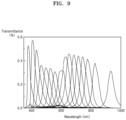
- the sensing spectra or wavelength bands of the RGB image sensor and the MSI sensor will be described later with reference to FIGS. 5 and 9 .
- the first image sensor 100 and the second image sensor 200 may be provided as separate chips or a single chip.
- timing control may be performed according to different resolutions and output speeds of different types of sensors and the size of a region required for image registration. For example, when reading an RGB image column in an operation based on the RGB image sensor, an image column of the MSI sensor, which corresponds to the RGB image column, may be previously stored in a buffer or may be read anew. Signals sensed by calculating such a timing may be read out. Alternatively, the operations of the two sensors may be synchronized using the same synchronization signal. In addition, focus control may be performed to focus both the sensors on the same position of an object.
- the MSI sensor may acquire an image through all the channels, for example, 16 channels, or through specific channels. Only specific channels may be used by binning sensor pixels, or selecting or synthesizing the specific channels.
- a first memory 300 stores the first image IM 1 read out from the first image sensor 100 .
- a second memory 310 stores the second image IM 2 read out from the second image sensor 200 .
- Images are read out on a line basis from the first image sensor 100 and the second image sensor 200 and are sequentially stored.
- the first memory 300 and the second memory 310 may be line memories for storing images on a line basis or frame buffers for storing the entire images.
- the first and second memories 300 and 310 may be static random access memories (SRAMs) or dynamic random access memories (DRAMs). However, the types of the first and second memories 300 and 310 are not limited.
- the first and second memories 300 and 310 may be provided outside the first and second image sensors 100 and 200 or may be integrated into the first and second image sensors 100 and 200 .
- a method of integrating a memory into a sensor by constructing each stack with a pixel unit, a circuit unit, and a memory, and integrating two stacks as one chip may be used.
- three layers respectively including a pixel unit, a circuit unit, and a memory may be formed as three stacks.
- the first image IM 1 and the second image IM 2 respectively acquired using the first image sensor 100 and the second image sensor 200 are stored in different memories, that is, the first memory 300 and the second memory 310 .
- the first image IM 1 and the second image IM 2 may be stored in one memory.
- the processor 500 includes an image registration unit 510 , an illumination estimation unit 520 , and a color conversion unit 530 .
- the processor 500 may further include an image signal processor (hereinafter referred to as an ISP).
- the ISP may perform a basic image processing process on images respectively acquired from the first image sensor 100 and the second image sensor 200 before or after the images are respectively stored in the first memory 300 and the second memory 310 .
- the ISP may perform bad pixel correction, fixed pattern noise correction, crosstalk reduction, remosaicing, demosaicing, false color reduction, denoising, chromatic aberration correction, or the like.
- the processor 500 or the ISP may perform the same image processing process or different image processing processes for the first image sensor 100 and the second image sensor 200 .
- the processor 500 may perform accurate white balancing by separating illumination from the color of an object by using the MSI sensor to find the exact color of the object, and then converting the color of an image acquired from the RGB image sensor or the color of a registration image by using an illumination value.
- the functions of the processor 500 will now be described.
- the image registration unit 510 registers the first image IM 1 and the second image IM 2 which are respectively output from the first image sensor 100 and the second image sensor 200 .
- the image registration unit 510 may register the first image IM 1 and the second image IM 2 by using information on the relative positions of the first image sensor 100 and the second image sensor 200 .
- the image registration unit 510 may find a positional relationship between image pixels by considering the spatial resolutions of images obtained using the first image sensor 100 and the second image sensor 200 , the field of view and focal length of an optical system used to capture the images, and the like.
- an image acquired using one sensor e.g., the first or second image sensor
- another image acquired using another sensor may be overlaid on the reference image.
- the first image IM 1 obtained using the first image sensor 100 may be set as a reference image, and pixels corresponding to the pixels of the first image IM 1 may be found from the pixels of the second image IM 2 obtained using the second image sensor 200 .
- scaling, translation, rotation, affine transform, perspective transform, or the like may be performed on the pixels of the second image IM 2 .
- a second image sample corresponding to the position of each pixel of the first image IM 1 may be generated for each channel by interpolation.
- the interpolation may be performed using bi-lateral filtering, guided filtering, or the like to consider edge information.
- image registration Before image registration, aberrations of the first image IM 1 and the second image IM 2 may be corrected. That is, image registration may be performed after correcting the influences of distortion, geometric aberrations, chromatic aberration, and the like, which are caused by lenses of the imaging optical systems used to obtain the first image IM 1 and the second image IM 2 .
- the display device ED 60 , etc. of the components may be omitted from the electronic apparatus ED 01 , or other components may be added to the electronic apparatus ED 01 .
- Some of the components may be implemented in one integrated circuit.
- the sensor module ED 76 a fingerprint sensor, an iris sensor, an illuminance sensor, etc.
- the display device ED 76 a display or the like.
- some sensor-module functions color sensing, illuminance sensing, etc.
- FIG. 15 is a block diagram schematically illustrating the camera module ED 80 included in the electronic apparatus ED 01 shown in FIG. 14 .
- the camera module ED 80 may include the image acquisition apparatus 1000 described above, or may have a structure modified therefrom.
- the camera module ED 80 may include a lens assembly CM 10 , a flash CM 20 , an image sensor CM 30 , an image stabilizer CM 40 , a memory CM 50 (a buffer memory, etc.), and/or an ISP CM 60 .
- the image sensor CM 30 may include the first image sensor 100 and the second image sensor 200 provided in the image acquisition apparatus 1000 described above.
- the first image sensor 100 and the second image sensor 200 may obtain an image corresponding to an object by converting light emitted or reflected from the object and transmitted through the lens assembly CM 10 into an electrical signal.
- the first image sensor 100 may obtain an RGB image
- the second image sensor 200 may obtain a hyperspectral image in an ultraviolet-to-infrared wavelength range.
- the image sensor CM 30 may further include one or more sensors selected from image sensors having different properties, such as another RGB image sensor, a black and white (BW) sensor, an infrared sensor, or an ultraviolet sensor.
- image sensors having different properties such as another RGB image sensor, a black and white (BW) sensor, an infrared sensor, or an ultraviolet sensor.
- BW black and white
- Each of the sensors included in the image sensor CM 30 may be implemented as a CCD sensor and/or a CMOS sensor.
- the lens assembly CM 10 may collect light coming from an object to be imaged.
- the camera module ED 80 may include a plurality of lens assemblies CM 10 , and in this case, the camera module ED 80 may be a dual camera, a 360-degree camera, or a spherical camera. Some of the plurality of lens assemblies CM 10 may have the same lens properties (field of view, focal length, autofocus, F Number, optical zoom, etc.) or different lens properties. Each of the lens assemblies CM 10 may include a wide-angle lens or a telephoto lens.
- the lens assembly CM 10 may be configured and/or focused such that two image sensors included in the image sensor CM 30 may form optical images of an object at the same position.
- the flash CM 20 may emit light used to enhance light emitted or reflected from an object.
- the flash CM 20 may include one or more light emitting diodes (a red-green-blue (RGB) LED, a white LED, an infrared LED, an ultraviolet LED, etc.), and/or a xenon lamp.
- RGB red-green-blue
- white LED a white LED
- infrared LED an ultraviolet LED, etc.
- a xenon lamp a xenon lamp.
- the image stabilizer CM 40 may move one or more lenses included in the lens assembly CM 10 or the image sensor CM 30 in a specific direction in response to a movement of the camera module ED 80 or the electronic apparatus ED 01 including the camera module ED 80 , or may control operating characteristics of the image sensor CM 30 (adjustment of read-out timing, etc.) to compensate for negative effects caused by movement.
- the image stabilizer CM 40 may detect a movement of the camera module ED 80 or the electronic apparatus ED 01 by using a gyro sensor (not shown) or an acceleration sensor (not shown) arranged inside or outside the camera module ED 80 .
- the image stabilizer CM 40 may be an optical image stabilizer.
- the memory CM 50 some or all of data obtained through the image acquisition apparatus 1000 may be stored for the next image processing operation. For example, when a plurality of images are obtained at a high speed, the obtained original data (Bayer-patterned data, high-resolution data, or the like) may be stored in the memory CM 50 and only a low-resolution image may be displayed. Then, the original data of a selected image (user selection, etc.) may be transferred to the ISP CM 60 .
- the memory CM 50 may be integrated into the memory ED 30 of the electronic apparatus ED 01 or may be configured as a separate memory that may be independently operated.
- the ISP CM 60 may perform one or more image processes on an image obtained through the image sensor CM 30 or image data stored in the memory CM 50 . As described with reference to FIGS. 1 to 13 , a first image (e.g., an RGB image) and a second image (e.g., an MSI image) obtained using two image sensors included in the image sensor CM 30 are processed to form a white-balanced third image. To this end, components of the processor 500 may be included in the ISP CM 60 .
- a first image e.g., an RGB image
- a second image e.g., an MSI image
- the one or more image processes may include depth map generation, three-dimensional modeling, panorama generation, feature point extraction, image synthesis, and/or image compensation (noise reduction, resolution adjustment, brightness adjustment, blurring, sharpening, softening, etc.).
- the ISP CM 60 may control (exposure time control, read-out timing control, etc.) components (the image sensor CM 30 , etc.) included in the camera module CM 80 .
- An image processed by the ISP CM 60 may be stored again in the memory CM 50 for additional processing or may be provided to external components (the memory ED 30 , the display device ED 60 , the electronic apparatus ED 02 , the electronic apparatus ED 04 , the server ED 08 , etc.) of the camera module ED 80 .
- the ISP CM 60 may be integrated into the processor ED 20 or may be configured as a separate processor that operates independently of the processor ED 20 .
- an image processed by the ISP CM 60 may be displayed on the display device ED 60 after being further processed by the processor ED 20 .
- the electronic apparatus ED 01 may include a plurality of camera modules ED 80 having different attributes or functions.
- one of the plurality of camera modules ED 80 may be a wide-angle camera, and another of the plurality of camera modules ED 80 may be a telephoto camera.
- one of the plurality of camera modules ED 80 may be a front camera, and another of the plurality of camera modules ED 80 may be a rear camera.
- FIGS. 16 to 25 are views illustrating various examples of an electronic apparatus to which the image acquisition apparatus 1000 is applied according to embodiments.
- the image acquisition apparatus 1000 may be applied to a mobile phone or smartphone 5100 m shown in FIG. 16 , a tablet or smart tablet 5200 shown in FIG. 17 , a digital camera or camcorder 5300 shown in FIG. 18 , a laptop computer 5400 shown in FIG. 19 , or a television or smart television 5500 shown in FIG. 20 .
- the smartphone 5100 m or the smart tablet 5200 may include a plurality of high-resolution cameras each having a high-resolution image sensor mounted thereon. The high-resolution cameras may be used to extract depth information of objects in an image, adjust out of focus of an image, or automatically identify objects in an image.
- the image acquisition apparatus 1000 may be applied to a smart refrigerator 5600 shown in FIG. 21 , a security camera 5700 shown in FIG. 22 , a robot 5800 shown in FIG. 23 , a medical camera 5900 shown in FIG. 24 , and the like.
- the smart refrigerator 5600 may automatically recognize food contained in the smart refrigerator 5600 by using the image acquisition apparatus 1000 , and may inform a user of whether a specific food is contained in the smart refrigerator 5600 , the type of food put into or out of the smart refrigerator 5600 , and the like through a smartphone.
- the security camera 5700 may provide an ultra-high-resolution image and may recognize an object or a person in the ultra-high-resolution image even in a dark environment owing to high sensitivity of the security camera 5700 .
- the robot 5800 may be sent to a disaster or industrial site that cannot be directly accessed by humans and may provide high-resolution images.
- the medical camera 5900 may provide a high-resolution image for diagnosis or surgery, and may have a dynamically adjustable field of view.
- the image acquisition apparatus 1000 may be applied to a vehicle 6000 as shown in FIG. 25 .
- the vehicle 6000 may include a plurality of vehicle cameras 6010 , 6020 , 6030 , and 6040 arranged at various positions. Each of the vehicle cameras 6010 , 6020 , 6030 , and 6040 may include an image acquisition apparatus according to an embodiment.
- the vehicle 6000 may use the vehicle cameras 6010 , 6020 , 6030 , and 6040 to provide a driver with various information about the interior or surroundings of the vehicle 6000 , and may provide information necessary for autonomous driving by automatically recognizing objects or people in images.
- the image acquisition apparatus may perform accurate white balancing even under one or more illumination lights without limitations by using two different types of image sensors.
- the image acquisition apparatus may be employed in various electronic apparatuses.
Landscapes
- Engineering & Computer Science (AREA)
- Multimedia (AREA)
- Signal Processing (AREA)
- Physics & Mathematics (AREA)
- Theoretical Computer Science (AREA)
- Human Computer Interaction (AREA)
- Spectroscopy & Molecular Physics (AREA)
- Data Mining & Analysis (AREA)
- Computing Systems (AREA)
- Biomedical Technology (AREA)
- Biophysics (AREA)
- Computational Linguistics (AREA)
- Life Sciences & Earth Sciences (AREA)
- Evolutionary Computation (AREA)
- General Health & Medical Sciences (AREA)
- Molecular Biology (AREA)
- Artificial Intelligence (AREA)
- General Engineering & Computer Science (AREA)
- General Physics & Mathematics (AREA)
- Mathematical Physics (AREA)
- Software Systems (AREA)
- Health & Medical Sciences (AREA)
- Color Television Image Signal Generators (AREA)
- Studio Devices (AREA)
Abstract
Description
p=∫E(λ)S(λ)R(λ)dλ [Equation 1]
I′=MI [Equation 5]
Claims (21)
Applications Claiming Priority (2)
| Application Number | Priority Date | Filing Date | Title |
|---|---|---|---|
| KR10-2021-0113981 | 2021-08-27 | ||
| KR1020210113981A KR102827126B1 (en) | 2021-08-27 | 2021-08-27 | Image acquisition apparatus including a plurality of image sensors and electronic apparatus including the same |
Publications (2)
| Publication Number | Publication Date |
|---|---|
| US20230066267A1 US20230066267A1 (en) | 2023-03-02 |
| US12267604B2 true US12267604B2 (en) | 2025-04-01 |
Family
ID=83360992
Family Applications (1)
| Application Number | Title | Priority Date | Filing Date |
|---|---|---|---|
| US17/831,956 Active 2042-09-23 US12267604B2 (en) | 2021-08-27 | 2022-06-03 | Image acquisition apparatus including a plurality of image sensors, and electronic apparatus including the image acquisition apparatus |
Country Status (5)
| Country | Link |
|---|---|
| US (1) | US12267604B2 (en) |
| EP (1) | EP4142300A1 (en) |
| JP (1) | JP7503104B2 (en) |
| KR (1) | KR102827126B1 (en) |
| CN (1) | CN115734082B (en) |
Families Citing this family (6)
| Publication number | Priority date | Publication date | Assignee | Title |
|---|---|---|---|---|
| CN118805067A (en) * | 2022-02-25 | 2024-10-18 | 松下知识产权经营株式会社 | Camera device |
| JP2024031119A (en) * | 2022-08-25 | 2024-03-07 | 富士フイルム株式会社 | Image processing device, image processing method, image processing program, and endoscope system |
| KR20240143540A (en) | 2023-03-24 | 2024-10-02 | 삼성전자주식회사 | Image acquisition apparatus and method of operation thereof |
| KR20240178111A (en) * | 2023-06-21 | 2024-12-30 | 삼성전자주식회사 | Apparatus and method for acquiring an image |
| GB2635154A (en) * | 2023-10-31 | 2025-05-07 | Sony Semiconductor Solutions Corp | An image sensor system, method of control and computer program |
| DE102024127402A1 (en) * | 2024-09-23 | 2025-07-10 | Bayerische Motoren Werke Aktiengesellschaft | METHOD AND DEVICE FOR OPTICALLY DETECTING AN INTERIOR OF A VEHICLE, AND VEHICLE AND COMPUTER PROGRAM PRODUCT |
Citations (22)
| Publication number | Priority date | Publication date | Assignee | Title |
|---|---|---|---|---|
| JP2004200885A (en) | 2002-12-17 | 2004-07-15 | Matsushita Electric Ind Co Ltd | Electronic equipment mounted imaging device |
| US20040246350A1 (en) * | 2003-06-04 | 2004-12-09 | Casio Computer Co. , Ltd. | Image pickup apparatus capable of reducing noise in image signal and method for reducing noise in image signal |
| US20090002475A1 (en) * | 2007-06-27 | 2009-01-01 | General Instrument Corporation | Apparatus and System for Improving Image Quality |
| US20090256927A1 (en) * | 2008-04-11 | 2009-10-15 | Olympus Corporation | Image capturing apparatus |
| US7701489B1 (en) | 2003-05-27 | 2010-04-20 | Apple Inc. | Method and apparatus for color correction |
| JP2011211317A (en) | 2010-03-29 | 2011-10-20 | Olympus Corp | Light source detector |
| CN102469243A (en) | 2010-11-04 | 2012-05-23 | 卡西欧计算机株式会社 | Image pickup device capable of adjusting white balance |
| JP2013024653A (en) * | 2011-07-19 | 2013-02-04 | Toyota Central R&D Labs Inc | Distance measuring apparatus and program |
| US20140078247A1 (en) * | 2012-09-18 | 2014-03-20 | Makoto Shohara | Image adjuster and image adjusting method and program |
| US20150070528A1 (en) * | 2012-10-23 | 2015-03-12 | Olympus Corporation | Imaging device and image generation method |
| US20170054966A1 (en) * | 2015-08-18 | 2017-02-23 | RGBDsense Information Technology Ltd. | Structured light encoding-based vertical depth perception apparatus |
| US20170180656A1 (en) * | 2015-12-16 | 2017-06-22 | Samsung Electronics Co., Ltd. | Image processing apparatus and image processing system |
| WO2018145576A1 (en) | 2017-02-10 | 2018-08-16 | 杭州海康威视数字技术股份有限公司 | Multi-spectrum-based image fusion apparatus and method, and image sensor |
| JP2018207497A (en) | 2018-07-19 | 2018-12-27 | キヤノン株式会社 | Image processing apparatus, image processing method, imaging apparatus, program, and storage medium |
| US20190045163A1 (en) * | 2018-10-02 | 2019-02-07 | Intel Corporation | Method and system of deep learning-based automatic white balancing |
| CN110533620A (en) | 2019-07-19 | 2019-12-03 | 西安电子科技大学 | A hyperspectral and panchromatic image fusion method based on AAE to extract spatial features |
| US20200389604A1 (en) | 2008-05-20 | 2020-12-10 | Fotonation Limited | Capturing and Processing of Images Including Occlusions Focused on an Image Sensor by a Lens Stack Array |
| US20210067712A1 (en) | 2019-08-30 | 2021-03-04 | Scholly Fiberoptic Gmbh | Sensor array, method for calculating a color image and a hyperspectral image, method for carrying out a white balance and use of the sensor array in medical imaging |
| WO2021037934A1 (en) | 2019-08-28 | 2021-03-04 | ams Sensors Germany GmbH | Systems for characterizing ambient illumination |
| US20220385864A1 (en) * | 2021-05-26 | 2022-12-01 | Samsung Electronics.,Co.,Ltd. | Image acquisition apparatus providing wide color gamut image and electronic apparatus including the same |
| US20230099629A1 (en) * | 2021-09-28 | 2023-03-30 | Samsung Electronics Co., Ltd. | Image acquisition apparatus providing white balance function and electronic apparatus including the same |
| US20230217088A1 (en) * | 2022-01-03 | 2023-07-06 | Samsung Electronics Co., Ltd. | Image acquisition apparatus and electronic apparatus including the same |
-
2021
- 2021-08-27 KR KR1020210113981A patent/KR102827126B1/en active Active
-
2022
- 2022-06-03 US US17/831,956 patent/US12267604B2/en active Active
- 2022-06-07 CN CN202210633355.9A patent/CN115734082B/en active Active
- 2022-08-16 JP JP2022129504A patent/JP7503104B2/en active Active
- 2022-08-26 EP EP22192380.8A patent/EP4142300A1/en active Pending
Patent Citations (24)
| Publication number | Priority date | Publication date | Assignee | Title |
|---|---|---|---|---|
| JP2004200885A (en) | 2002-12-17 | 2004-07-15 | Matsushita Electric Ind Co Ltd | Electronic equipment mounted imaging device |
| US7701489B1 (en) | 2003-05-27 | 2010-04-20 | Apple Inc. | Method and apparatus for color correction |
| US20040246350A1 (en) * | 2003-06-04 | 2004-12-09 | Casio Computer Co. , Ltd. | Image pickup apparatus capable of reducing noise in image signal and method for reducing noise in image signal |
| US20090002475A1 (en) * | 2007-06-27 | 2009-01-01 | General Instrument Corporation | Apparatus and System for Improving Image Quality |
| US20090256927A1 (en) * | 2008-04-11 | 2009-10-15 | Olympus Corporation | Image capturing apparatus |
| US20200389604A1 (en) | 2008-05-20 | 2020-12-10 | Fotonation Limited | Capturing and Processing of Images Including Occlusions Focused on an Image Sensor by a Lens Stack Array |
| JP2011211317A (en) | 2010-03-29 | 2011-10-20 | Olympus Corp | Light source detector |
| CN102469243A (en) | 2010-11-04 | 2012-05-23 | 卡西欧计算机株式会社 | Image pickup device capable of adjusting white balance |
| US20140293089A1 (en) * | 2010-11-04 | 2014-10-02 | Casio Computer Co., Ltd. | Image capturing apparatus capable of adjusting white balance |
| JP2013024653A (en) * | 2011-07-19 | 2013-02-04 | Toyota Central R&D Labs Inc | Distance measuring apparatus and program |
| US20140078247A1 (en) * | 2012-09-18 | 2014-03-20 | Makoto Shohara | Image adjuster and image adjusting method and program |
| US20150070528A1 (en) * | 2012-10-23 | 2015-03-12 | Olympus Corporation | Imaging device and image generation method |
| US20170054966A1 (en) * | 2015-08-18 | 2017-02-23 | RGBDsense Information Technology Ltd. | Structured light encoding-based vertical depth perception apparatus |
| US20170180656A1 (en) * | 2015-12-16 | 2017-06-22 | Samsung Electronics Co., Ltd. | Image processing apparatus and image processing system |
| WO2018145576A1 (en) | 2017-02-10 | 2018-08-16 | 杭州海康威视数字技术股份有限公司 | Multi-spectrum-based image fusion apparatus and method, and image sensor |
| US20190378257A1 (en) | 2017-02-10 | 2019-12-12 | Hangzhou Hikvision Digital Technology Co., Ltd. | Multi-spectrum-based image fusion apparatus and method, and image sensor |
| JP2018207497A (en) | 2018-07-19 | 2018-12-27 | キヤノン株式会社 | Image processing apparatus, image processing method, imaging apparatus, program, and storage medium |
| US20190045163A1 (en) * | 2018-10-02 | 2019-02-07 | Intel Corporation | Method and system of deep learning-based automatic white balancing |
| CN110533620A (en) | 2019-07-19 | 2019-12-03 | 西安电子科技大学 | A hyperspectral and panchromatic image fusion method based on AAE to extract spatial features |
| WO2021037934A1 (en) | 2019-08-28 | 2021-03-04 | ams Sensors Germany GmbH | Systems for characterizing ambient illumination |
| US20210067712A1 (en) | 2019-08-30 | 2021-03-04 | Scholly Fiberoptic Gmbh | Sensor array, method for calculating a color image and a hyperspectral image, method for carrying out a white balance and use of the sensor array in medical imaging |
| US20220385864A1 (en) * | 2021-05-26 | 2022-12-01 | Samsung Electronics.,Co.,Ltd. | Image acquisition apparatus providing wide color gamut image and electronic apparatus including the same |
| US20230099629A1 (en) * | 2021-09-28 | 2023-03-30 | Samsung Electronics Co., Ltd. | Image acquisition apparatus providing white balance function and electronic apparatus including the same |
| US20230217088A1 (en) * | 2022-01-03 | 2023-07-06 | Samsung Electronics Co., Ltd. | Image acquisition apparatus and electronic apparatus including the same |
Non-Patent Citations (11)
| Title |
|---|
| Communication issued Aug. 23, 2024 by the China National Intellectual Property Administration in Chinese Patent Application No. 202210633355.9. |
| David J Brady et al., "Smart Cameras", Image and Video Processing (eess.IV), arXiv:2002.04705v1, Feb. 11, 2020, 55 Pages, XP081597787. |
| European Extended Search Report issued Feb. 12, 2025 by the European Patent Office for EP Patent Application No. 22192380.8. |
| Extended European Search Report issued by the European Patent Office on Jan. 24, 2023 for European Patent Application No. 22192380.8. |
| ISO and CIE, "Colorimetry—Part 6: CIEDE2000 Colour-difference formula," ISO/CIE 11664-6:2014(E), First Edition, Feb. 1, 2014, 18 Pages. |
| Ji-Won Lee et al., "Estimation of Illumination Spectrum from a Hyperspectral Image", IEIE Transactions on Smart Processing and Computing, vol. 8, Issue No. 2, Apr. 2019, pp. 95-99. |
| Kobus Barnard et al., "A Comparison of Computational Color Constancy Algorithms—Part I: Methodology and Experiments With Synthesized Data", IEEE Transactions on Image Processing, vol. 11, Issue No. 9, Sep. 2002, pp. 972-983. |
| Laurence T Maloney et al., "Color constancy: a method for recovering surface spectral reflectance", Journal of the Optical Society of America A, vol. 3, Issue No. 1, Jan. 1986, pp. 29-33. |
| Office Action dated Nov. 28, 2023, issued by Japanese Patent Office in Japanese Patent Application No. 2022-129504. |
| Office Action issued on Jan. 24, 2025 by the Chinese Patent Office in corresponding CN Patent Application No. 202210633355.9. |
| Yinqiang Zheng et al., "Illumination and Reflectance Spectra Separation of a Hyperspectral Image Meets Low-Rank Matrix Factorization" IEEE Conference on Computer Vision and Pattern Recognition (CVPR), Oct. 2015, pp. 1779-1787. |
Also Published As
| Publication number | Publication date |
|---|---|
| JP7503104B2 (en) | 2024-06-19 |
| CN115734082B (en) | 2025-06-03 |
| US20230066267A1 (en) | 2023-03-02 |
| KR102827126B1 (en) | 2025-07-01 |
| JP2023033168A (en) | 2023-03-09 |
| EP4142300A1 (en) | 2023-03-01 |
| KR20230031580A (en) | 2023-03-07 |
| CN115734082A (en) | 2023-03-03 |
Similar Documents
| Publication | Publication Date | Title |
|---|---|---|
| US12267604B2 (en) | Image acquisition apparatus including a plurality of image sensors, and electronic apparatus including the image acquisition apparatus | |
| EP4207099B1 (en) | Image acquisition apparatus and electronic apparatus including the same | |
| JP7504170B2 (en) | Image acquisition device for performing white balance, electronic device including same, and method for controlling image acquisition device | |
| US12363451B2 (en) | Color interpolation method for multispectral filter array and image acquisition device | |
| EP4096213B1 (en) | Image acquisition apparatus providing wide color gamut image and electronic apparatus including the same | |
| KR102667267B1 (en) | Image acquisition apparatus and electronic apparatus including the same | |
| EP4436164B1 (en) | Image acquisition apparatus and method of operating the same | |
| US12532054B2 (en) | Image acquisition apparatus and method of acquiring images using a multispectral image sensor | |
| US20250131532A1 (en) | Image acquisition device and electronic device including the same |
Legal Events
| Date | Code | Title | Description |
|---|---|---|---|
| AS | Assignment |
Owner name: SAMSUNG ELECTRONICS CO., LTD., KOREA, REPUBLIC OF Free format text: ASSIGNMENT OF ASSIGNORS INTEREST;ASSIGNORS:KIM, WOO-SHIK;ROH, YOUNGGEUN;RYU, INHWAN;SIGNING DATES FROM 20220221 TO 20220505;REEL/FRAME:060099/0420 |
|
| FEPP | Fee payment procedure |
Free format text: ENTITY STATUS SET TO UNDISCOUNTED (ORIGINAL EVENT CODE: BIG.); ENTITY STATUS OF PATENT OWNER: LARGE ENTITY |
|
| STPP | Information on status: patent application and granting procedure in general |
Free format text: DOCKETED NEW CASE - READY FOR EXAMINATION |
|
| STPP | Information on status: patent application and granting procedure in general |
Free format text: NON FINAL ACTION MAILED |
|
| STPP | Information on status: patent application and granting procedure in general |
Free format text: RESPONSE TO NON-FINAL OFFICE ACTION ENTERED AND FORWARDED TO EXAMINER |
|
| STPP | Information on status: patent application and granting procedure in general |
Free format text: NOTICE OF ALLOWANCE MAILED -- APPLICATION RECEIVED IN OFFICE OF PUBLICATIONS |
|
| STPP | Information on status: patent application and granting procedure in general |
Free format text: AWAITING TC RESP., ISSUE FEE NOT PAID |
|
| STPP | Information on status: patent application and granting procedure in general |
Free format text: NOTICE OF ALLOWANCE MAILED -- APPLICATION RECEIVED IN OFFICE OF PUBLICATIONS |
|
| STPP | Information on status: patent application and granting procedure in general |
Free format text: PUBLICATIONS -- ISSUE FEE PAYMENT VERIFIED |
|
| STPP | Information on status: patent application and granting procedure in general |
Free format text: PUBLICATIONS -- ISSUE FEE PAYMENT VERIFIED |
|
| STCF | Information on status: patent grant |
Free format text: PATENTED CASE |