US12260129B2 - Tracking and updating read command voltage thresholds in solid-state drives - Google Patents
Tracking and updating read command voltage thresholds in solid-state drives Download PDFInfo
- Publication number
- US12260129B2 US12260129B2 US18/124,407 US202318124407A US12260129B2 US 12260129 B2 US12260129 B2 US 12260129B2 US 202318124407 A US202318124407 A US 202318124407A US 12260129 B2 US12260129 B2 US 12260129B2
- Authority
- US
- United States
- Prior art keywords
- controller
- block
- read
- threshold
- voltage threshold
- Prior art date
- Legal status (The legal status is an assumption and is not a legal conclusion. Google has not performed a legal analysis and makes no representation as to the accuracy of the status listed.)
- Active, expires
Links
Images


Classifications
-
- G—PHYSICS
- G06—COMPUTING OR CALCULATING; COUNTING
- G06F—ELECTRIC DIGITAL DATA PROCESSING
- G06F11/00—Error detection; Error correction; Monitoring
- G06F11/07—Responding to the occurrence of a fault, e.g. fault tolerance
- G06F11/08—Error detection or correction by redundancy in data representation, e.g. by using checking codes
- G06F11/10—Adding special bits or symbols to the coded information, e.g. parity check, casting out 9's or 11's
- G06F11/1008—Adding special bits or symbols to the coded information, e.g. parity check, casting out 9's or 11's in individual solid state devices
- G06F11/1048—Adding special bits or symbols to the coded information, e.g. parity check, casting out 9's or 11's in individual solid state devices using arrangements adapted for a specific error detection or correction feature
-
- G—PHYSICS
- G06—COMPUTING OR CALCULATING; COUNTING
- G06F—ELECTRIC DIGITAL DATA PROCESSING
- G06F11/00—Error detection; Error correction; Monitoring
- G06F11/07—Responding to the occurrence of a fault, e.g. fault tolerance
- G06F11/08—Error detection or correction by redundancy in data representation, e.g. by using checking codes
- G06F11/10—Adding special bits or symbols to the coded information, e.g. parity check, casting out 9's or 11's
- G06F11/1008—Adding special bits or symbols to the coded information, e.g. parity check, casting out 9's or 11's in individual solid state devices
- G06F11/1068—Adding special bits or symbols to the coded information, e.g. parity check, casting out 9's or 11's in individual solid state devices in sector programmable memories, e.g. flash disk
-
- G—PHYSICS
- G06—COMPUTING OR CALCULATING; COUNTING
- G06F—ELECTRIC DIGITAL DATA PROCESSING
- G06F3/00—Input arrangements for transferring data to be processed into a form capable of being handled by the computer; Output arrangements for transferring data from processing unit to output unit, e.g. interface arrangements
- G06F3/06—Digital input from, or digital output to, record carriers, e.g. RAID, emulated record carriers or networked record carriers
- G06F3/0601—Interfaces specially adapted for storage systems
- G06F3/0602—Interfaces specially adapted for storage systems specifically adapted to achieve a particular effect
- G06F3/061—Improving I/O performance
-
- G—PHYSICS
- G06—COMPUTING OR CALCULATING; COUNTING
- G06F—ELECTRIC DIGITAL DATA PROCESSING
- G06F3/00—Input arrangements for transferring data to be processed into a form capable of being handled by the computer; Output arrangements for transferring data from processing unit to output unit, e.g. interface arrangements
- G06F3/06—Digital input from, or digital output to, record carriers, e.g. RAID, emulated record carriers or networked record carriers
- G06F3/0601—Interfaces specially adapted for storage systems
- G06F3/0628—Interfaces specially adapted for storage systems making use of a particular technique
- G06F3/0655—Vertical data movement, i.e. input-output transfer; data movement between one or more hosts and one or more storage devices
- G06F3/0659—Command handling arrangements, e.g. command buffers, queues, command scheduling
-
- G—PHYSICS
- G06—COMPUTING OR CALCULATING; COUNTING
- G06F—ELECTRIC DIGITAL DATA PROCESSING
- G06F3/00—Input arrangements for transferring data to be processed into a form capable of being handled by the computer; Output arrangements for transferring data from processing unit to output unit, e.g. interface arrangements
- G06F3/06—Digital input from, or digital output to, record carriers, e.g. RAID, emulated record carriers or networked record carriers
- G06F3/0601—Interfaces specially adapted for storage systems
- G06F3/0668—Interfaces specially adapted for storage systems adopting a particular infrastructure
- G06F3/0671—In-line storage system
- G06F3/0673—Single storage device
- G06F3/0679—Non-volatile semiconductor memory device, e.g. flash memory, one time programmable memory [OTP]
-
- G—PHYSICS
- G11—INFORMATION STORAGE
- G11C—STATIC STORES
- G11C11/00—Digital stores characterised by the use of particular electric or magnetic storage elements; Storage elements therefor
- G11C11/56—Digital stores characterised by the use of particular electric or magnetic storage elements; Storage elements therefor using storage elements with more than two stable states represented by steps, e.g. of voltage, current, phase, frequency
- G11C11/5621—Digital stores characterised by the use of particular electric or magnetic storage elements; Storage elements therefor using storage elements with more than two stable states represented by steps, e.g. of voltage, current, phase, frequency using charge storage in a floating gate
- G11C11/5642—Sensing or reading circuits; Data output circuits
-
- G—PHYSICS
- G11—INFORMATION STORAGE
- G11C—STATIC STORES
- G11C11/00—Digital stores characterised by the use of particular electric or magnetic storage elements; Storage elements therefor
- G11C11/56—Digital stores characterised by the use of particular electric or magnetic storage elements; Storage elements therefor using storage elements with more than two stable states represented by steps, e.g. of voltage, current, phase, frequency
- G11C11/5671—Digital stores characterised by the use of particular electric or magnetic storage elements; Storage elements therefor using storage elements with more than two stable states represented by steps, e.g. of voltage, current, phase, frequency using charge trapping in an insulator
-
- G—PHYSICS
- G11—INFORMATION STORAGE
- G11C—STATIC STORES
- G11C16/00—Erasable programmable read-only memories
- G11C16/02—Erasable programmable read-only memories electrically programmable
- G11C16/04—Erasable programmable read-only memories electrically programmable using variable threshold transistors, e.g. FAMOS
- G11C16/0483—Erasable programmable read-only memories electrically programmable using variable threshold transistors, e.g. FAMOS comprising cells having several storage transistors connected in series
-
- G—PHYSICS
- G11—INFORMATION STORAGE
- G11C—STATIC STORES
- G11C16/00—Erasable programmable read-only memories
- G11C16/02—Erasable programmable read-only memories electrically programmable
- G11C16/06—Auxiliary circuits, e.g. for writing into memory
- G11C16/26—Sensing or reading circuits; Data output circuits
Definitions
- the present disclosure relates to solid-state drives (SSDs) and methods for tracking and updating read voltage thresholds to ensure successful read commands and improve system performance.
- SSDs solid-state drives
- Data retention stress is caused by long periods of time that elapse between programming operations of an MLC NAND device and subsequent read operations from the device. During such periods, data that was stored on a flash page is gradually lost due to electron detrapping. This causes leakage of charge out of the memory cell, and, as such, the voltage level of each cell gradually decreases. In other words, data retention stresses thus cause the voltage distributions corresponding to particular MLC states to shift to lower voltages. As a consequence of such shifting, erroneous data may be read.
- a nonvolatile memory device comprising a plurality of memory dies. Each of the memory dies comprises a plurality of blocks.
- the nonvolatile memory device further comprises a controller coupled to the plurality of memory dies.
- the controller is configured to read, from a first block of the plurality of blocks, data corresponding to a read command received from a host.
- the controller is also configured to determine a bit error rate for the first block based on the data.
- the controller is further configured to update a read voltage threshold for the first block when the bit error rate for the first block exceeds a first error threshold.
- FIGS. 2 A- 2 C illustrate exemplary voltage threshold distributions in MLC NAND cells subject to no stress, data retention stress, and read disturb stress
- FIGS. 3 A and 3 B illustrate a history table and a code book table (together a “code book”) for use in the read voltage threshold updating and tracking methods according to one or more embodiments of the disclosure;
- FIGS. 4 H- 4 J illustrate data showing the effect of various stresses on read voltage threshold distributions
- FIG. 5 illustrates a table containing stress impacts, ECC statistics, and offset values for the stress cases of FIGS. 4 B- 4 G according to one or more embodiments of the disclosure
- FIG. 6 illustrates an exemplary SSD processing read commands to several NAND devices in parallel according to one or more embodiments of the disclosure
- FIG. 7 illustrates an exemplary SSD configured to store ECC statistics for multiple blocks of multiple NAND devices according to one or more embodiments of the disclosure
- FIG. 8 illustrates the relationship between BER and time for the case of an SSD using default read thresholds and for the case of an SSD using the tracking and updating methods according to one or more embodiments of the disclosure.
- FIG. 9 illustrates a flowchart illustrating the tracking and updating methods according to one or more embodiments of the disclosure.
- SSD solid-state drive
- all the components and other features outlined below may be implemented in a variety of fashions in either hardware or firmware of an SSD in any suitable manner, and may be adapted and applied to other types of SSD architectures having a similar need to avoid burdensome read retry flows caused by executing read commands based on a default threshold.
- all of the components and other features outlined below may be implemented in other types of nonvolatile memory devices, including universal flash storage (UFS) devices or secure digital (SD) card devices.
- UFS universal flash storage
- SD secure digital
- the present disclosure provides a method for tracking a threshold voltage used to read data from a NAND device by a controller of an SSD, and for updating the threshold voltage in the event that the data read from the NAND device has a corresponding bit error rate (BER) that exceeds some threshold.
- BER bit error rate
- the threshold tracking mechanism exploits the relationship between MLC NAND flash characteristics and different stress conditions.
- the failed bit count (FBC) results of ECC in the upper and lower pages of MLC NAND flash and stress type and magnitude are correlated.
- the tracking mechanism uses this correlation, as well as ECC decoding statistics of pages that have already been read and decoded in a standard, functional read flow, to estimate new read-thresholds.
- Such thresholds can be estimated, optimized, and adjusted to yield a BER that can be corrected by ECC, so that retry flows are not invoked.
- the read threshold tracking/adaptation mechanism and BER estimation method are simple and effective, and can be implemented both in hardware or firmware.
- tracking mechanisms can be done with zero overhead: no additional buffer or NAND reads are required, as the statistics on which the estimations are based are gathered contemporaneously with the issued functional read commands.
- the tracking mechanisms described herein improve system performance and enable working with a higher endurance, as occurrences read-retry events followed by reading pages with default read-thresholds are reduced).
- the result is optimized quality of service (QOS) and continuous, successful hard-decoding due to the matching of stresses and thresholds.
- QOS quality of service
- FIG. 1 is a block diagram of a memory system comprising an SSD 100 in communication with a host 105 .
- the host 105 may be a computing system that comprises processors, memories, and other components as generally known in the art. Such components of the host 105 are not illustrated in FIG. 1 for the sake of brevity.
- SSD 100 may communicate with host 105 via a host interface 120 .
- SSD 100 may further comprise a controller 110 , which itself may comprise a codebook 112 , a processor 114 , and an ECC module 116 .
- Codebook 112 is, in some embodiments, a data structure in which information regarding read voltage thresholds is accessed, stored, and updated as described herein.
- Codebook 112 may be embodied as a storage component on controller 110 , or may be implemented as a component of processor 114 .
- ECC module 116 is, in some embodiments, a component of controller 110 configured to implement ECC on the codewords read from NAND devices 140 of SSD 100 .
- ECC module 116 provides statistics on the BERs of the blocks of the NAND devices 140 , as ascertained from the results of the ECC applied to the codewords read therefrom.
- ECC module 116 may be implemented as hardware, software, or as a combination of both hardware and software.
- Controller 110 is configured to track the threshold voltages used to execute read commands received from host 105 , and, in some embodiments, is further configured to update the threshold voltages based on the block BER statistics determined by ECC module 116 .
- Controller 110 communicates via NAND interface 130 with a plurality of nonvolatile memory devices 140 . While FIG. 1 shows that SSD 100 comprises NAND devices 140 , other nonvolatile memory devices could be implemented in SSD 100 without loss of generality.
- Controller 110 may be implemented as a system-on-a-chip (SoC).
- SoCs are advantageous as they provide a single integrated circuit that contains all of the circuitry and components of the electronic system for SSD 100 to function.
- FIGS. 2 A- 2 C represent illustrative voltage threshold distributions used to read data from multi-level cell (MLC) NAND devices with four programmable states.
- MLC multi-level cell
- DR data retention
- RD read disturb
- FIGS. 2 A- 2 C represent illustrative voltage threshold distributions used to read data from multi-level cell (MLC) NAND devices with four programmable states.
- DR data retention
- RD read disturb
- FIG. 2 A demonstrates an exemplary voltage threshold distribution used to read data from an MLC NAND device in the absence of stress.
- FIG. 2 A has four voltage threshold lobes: 201 , 202 , 203 , and 204 .
- FIG. 2 A further shows three voltage thresholds: T 0 , T 1 , and T 2 .
- T 0 To read data from the lower page, the device may use threshold T 0 .
- Thresholds T 1 and T 2 are used to read data from the upper page of the device.
- the lowermost lobe 201 represents an “erase” state.
- FIG. 2 B demonstrates the effect of data retention stresses on the exemplary voltage threshold distribution of FIG. 2 A . Electron detrapping caused by large elapsed times between programming operations and read operations may cause lobes 202 ′ and 203 ′ to shift leftwards, towards lower voltages.
- T 1 when a read operation is performed on an MLC NAND device subject to data retention stresses using default threshold T 1 , the result might erroneously read the state of the upper page of the cell to be a ‘1’ when, in actuality, the upper page was programmed to state ‘0’.
- the state of the lower page may be erroneously read as a ‘1’ when, in actuality, the lower page was programmed to state ‘0’.
- FIG. 2 C demonstrates the effect of read disturb stresses on the exemplary voltage threshold distribution of FIG. 2 A .
- Pass-through voltages applied to cells sharing a common bit line with a cell subject to a read operation cause lobes 201 ′′ and 202 ′′ to shift rightwards, towards higher voltages.
- T 1 default threshold
- the result might erroneously read the state of the upper page of the cell to be a ‘0’ when, in actuality, the upper page was programmed to state ‘1’.
- the state of the lower page may be erroneously read as a ‘0’ when, in actuality, the lower page was programmed to state ‘1’.
- controller 110 of SSD 100 of FIG. 1 comprises a codebook 112 , a processor 114 , and ECC module 116 . Exemplary tracking and updating operations of controller 110 by codebook 112 , processor 114 , and ECC module 116 are described below with respect to FIGS. 3 - 9 .
- FIGS. 3 A and 3 B illustrate in detail an exemplary codebook 112 for use in such a tracking mechanism.
- the codebook 112 of FIGS. 3 A and 3 B may be, in some embodiments, configured for use as the codebook 112 of FIG. 1 .
- codebook 112 may be stored in controller 110 .
- FIG. 3 A represents a history table 302
- FIG. 3 B represents a codebook table 304 .
- History table 302 keeps, for each combination block and die of an MLC NAND device, an entry pointing a specific entry in codebook table 304 .
- Codebook table 304 contains up-to-date read thresholds associated with a particular stress for each block.
- the up-to-date read threshold can be selected, from codebook table 304 , based on the particular combination of block and die of interest in history table 302 .
- Both of history table 302 and codebook table 304 may be implemented in codebook 112 as look-up tables.
- the exemplary codebook 112 of FIGS. 3 A and 3 B assumes that the MLC NAND system has four NAND dies, each die having 8 blocks. However, the codebook of FIGS. 3 A and 3 B could be implemented in any configuration of MLC NAND without loss of generality.
- history table 302 is of size 32 ⁇ 4: there are 32 blocks in the exemplary system of the embodiment, and each corresponding entry to the history table has 4 bits.
- Codebook table 304 has size 16 ⁇ 39: there are 16 entries in the table, each entry corresponding to 3 read thresholds (as described above with respect to FIGS.
- each read threshold corresponds to 13 bits that represents a threshold voltage level ranging from, for example, 0 to 8,192 mV.
- the entries of codebook table 304 of FIG. 3 B are arranged in ascending order between and within each threshold, any suitable ordering of codebook table entries can be implemented.
- ⁇ TQ, T 1 j , T 2 k ⁇ , for 0 ⁇ i,j,k, ⁇ 3 the content of codebook table 304 is set using a for loop as described by exemplary code:
- the entries in codebook table 304 are updated over time in response to ECC statistics of codewords from pages that are read and decoded in standard, functional read flows.
- the updated entries to codebook table 304 are voltages that, when applied to read commands, return codewords having BERs that are correctable by ECC, as described herein.
- a read threshold update trigger indication is asserted by ECC statistics, a new codebook index can be found.
- the new codebook index may point to an entry in codebook table 304 that provides threshold more appropriate for the actual stress.
- the stress on each MLC NAND device can be analyzed, and a subsequent adjustment, or offset, to the stored read voltage threshold can be calculated.
- the BER corresponding to a codeword read from each block of a particular NAND device in response to a read command can be calculated, and a new threshold voltage can be calculated so as to lower the BER of subsequent codewords read by subsequent read commands executed on the block.
- the updated read voltage threshold VT Updated may be calculated based on the stored read voltage threshold VT Stored as described above with respect to FIG. 3 B , and the offset ⁇ VT in accordance with exemplary formula 2:
- VT update VT stored + ⁇ ⁇ VT . ( 2 )
- the offset ⁇ VT may be further calculated in accordance with exemplary formula 3:
- ⁇ T 0 , ⁇ T 1 , and ⁇ T 2 represent offset values that are equal to 0, 1, or ⁇ 1, depending on the type and magnitude of the stress to which the MLC NAND device is subject.
- positive offset values may be implemented when a system is subject to read disturb stress (as read disturb stress has the tendency to increase the voltage of all memory cells), and negative offset values may be implemented when a system is subject to data retention stress (as data retention stress has the tendency to reduce the voltage of all memory cells).
- the offset values used may be of magnitude 1.
- ⁇ T 0 , ⁇ T 1 , and ⁇ T 2 may in general be any integer values in proportion to
- FIGS. 4 A- 4 J demonstrate various different cases of RD and DR stresses
- FIG. 5 describes, for the cases of FIGS. 4 B- 4 G , the impact of the stress on the states of each page, statistical observations for ECC applied to each such page, and the offset values that are used in the calculation of ⁇ VT.
- FIG. 4 A again reproduces the exemplary voltage threshold distribution used to read data from an MLC NAND device in the absence of stress.
- FIG. 4 B demonstrates the effect of RD stress on the system of FIG. 4 A .
- lobe 405 has shifted to the right, relative to unstressed lobe 401 in FIG. 4 A .
- Row 509 of the table in FIG. 5 describes the stress impact, ECC statistical observations, and offset values for calculation of ⁇ VT for FIG. 4 B .
- the lower page of the read block is unaffected (column 506 ), but data may be erroneously read from the upper page using threshold T 1 .
- 4 B may return a ‘0’ from the upper page of the block, when in actuality the state was programmed to a ‘1’ (column 508 ).
- Reads from the upper page using threshold T 2 are unaffected (column 510 ).
- the BER is low (“L”, column 512 ) and, as such, there is a small probability that, for the lower page, any data will be erroneously read (column 514 ).
- H high probability
- ECC will detect more ‘1’s erroneously read as ‘0’s (“P 0 ”) than it will ‘0’s erroneously read as ‘1’s (“P 1 ”). Accordingly, for the upper page in the case of FIG. 4 B , P 0 >P 1 (column 518 ). Finally, for the case of FIG. 4 B , because the erroneous reads arise from the voltage threshold increasing beyond threshold T 1 , the updated read voltage threshold should be increased to prevent such errors. Accordingly, the offset ⁇ VT is computed using a value of 1 for ⁇ T 1 .
- FIG. 4 C demonstrates another effect of RD stress on the system of FIG. 4 A .
- FIG. 4 C it can be seen that both lobes 409 and 410 have shifted to the right, relative to unstressed lobes 401 and 402 in FIG. 4 A .
- Row 511 of the table in FIG. 5 describes the stress impact, ECC statistical observations, and offset values for calculation of ⁇ VT for FIG. 4 C .
- data may be erroneously read from the lower page using threshold T 0 .
- a read command executed using threshold T 1 may also return a ‘0’ from the upper page of the block when the page was programmed to a ‘1’ (column 508 ).
- Reads from the upper page using threshold T 2 are unaffected (column 510 ).
- the BER is high (“H”, column 512 ) and, ECC will detect more ‘1’s erroneously read as ‘0’s (“P 0 ”) than it will ‘0’s erroneously read as ‘1’s (“P 1 ”). Accordingly, for the lower page in the case of FIG.
- FIG. 4 D demonstrates a third case of RD stress on the system of FIG. 4 A .
- lobes 413 , 414 , and 415 have shifted to the right, relative to unstressed lobes 401 , 402 , and 403 in FIG. 4 A .
- Row 513 of the table in FIG. 5 describes the stress impact, ECC statistical observations, and offset values for calculation of ⁇ VT for FIG. 4 D .
- data may be erroneously read from the lower page using threshold T 0 .
- a read command executed using threshold T 1 may also return a ‘0’ from the upper page of the block when the page was programmed to a ‘1’ (column 508 ).
- a read command executed using threshold T 2 may return a ‘1’ from the upper page of the block when the page was programmed to a ‘0’ (column 510 ).
- BER is high (“H”, columns 512 and 516 ).
- FIG. 4 E demonstrates an effect of DR stress on the system of FIG. 4 A .
- FIG. 4 E it can be seen that both lobes 418 and 419 have shifted to the left, relative to unstressed lobes 402 and 403 in FIG. 4 A .
- Row 515 of the table in FIG. 5 describes the stress impact, ECC statistical observations, and offset values for calculation of ⁇ VT for FIG. 4 E .
- data may be erroneously read from the lower page using threshold T 0 .
- a read command executed using threshold T 1 may also return a ‘1’ from the upper page of the block when the page was programmed to a ‘0’ (column 508 ).
- Reads from the upper page using threshold T 2 are unaffected (column 510 ).
- the BER is high (“H”, column 512 ) and, ECC will detect more ‘0’s erroneously read as ‘1’s (“P 1 ”) than it will ‘1’s erroneously read as ‘O’s (“P 0 ”). Accordingly, for the lower page in the case of FIG.
- FIG. 4 F demonstrates another effect of DR stress on the system of FIG. 4 A .
- FIG. 4 F it can be seen that lobes 422 , 423 , and 424 have shifted to the left, relative to unstressed lobes 402 , 403 , and 404 in FIG. 4 A .
- Row 517 of the table in FIG. 5 describes the stress impact, ECC statistical observations, and offset values for calculation of ⁇ VT for FIG. 4 F .
- data may be erroneously read from the lower page using threshold T 0 .
- 4 F may return a ‘1’ from the lower page of the block when the page was programmed to a ‘0’ (column 506 ). Further, a read command executed using threshold T 1 may also return a ‘1’ from the upper page of the block when the page was programmed to a ‘0’ (column 508 ). A read command executed using threshold T 2 may return a ‘0’ from the upper page of the block when the page was programmed to a ‘1’ (column 510 ).
- the BER is high (“H”, column 512 ) and, ECC will detect more ‘0’s erroneously read as ‘1’s (“P 1 ”) than it will ‘I’s erroneously read as ‘0’s (“P 0 ”). Accordingly, for the lower page in the case of FIG. 4 F , P 0 ⁇ P 1 (column 514 ). Further, there is a high probability (“H”, column 516 ) that data will be erroneously read from the upper page. In the upper page, because both read thresholds T 1 and T 2 are affected by the DR stress of FIG. 4 F , ‘1’s and ‘0’s will be erroneously read with a roughly similar frequency.
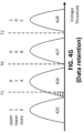
- FIG. 4 G demonstrates another effect of DR stress on the system of FIG. 4 A .
- lobe 426 has shifted to the left, relative to unstressed lobe 402 in FIG. 4 A .
- Row 519 of the table in FIG. 5 describes the stress impact, ECC statistical observations, and offset values for calculation of ⁇ VT for FIG. 4 G .
- reads from the lower page of the MLC NAND device are unaffected (column 506 ).
- a read command executed using threshold T 1 may return a ‘1’ from the upper page of the block when the page was programmed to a ‘0’ (column 508 ).
- a read command executed on the upper page of the MLC NAND device using threshold T 2 will also be unaffected (column 510 ).
- the BER is low (“L”, column 512 ) and, there is a small probability that ECC will erroneous bits (column 514 ).
- H high probability
- P 1 ECC will detect more ‘0’s erroneously read as ‘1’s (“P 1 ”) than it will ‘1’s erroneously read as ‘0’s (“P 0 ”), P 0 ⁇ P 1 (column 518 ).
- the offset ⁇ VT is computed using a value of ⁇ 1 for ⁇ T 1 .
- FIG. 4 H demonstrates data taken of a voltage threshold distribution from a SSD subject to one year of data retention stress and one program/erase cycle. It can be observed that reading this page with default read voltage thresholds provides no errors, as none of lobes 429 , 430 , or 431 shift past the delineated thresholds marked by vertical lines.
- FIG. 4 I demonstrates data taken of a voltage threshold distribution from a SSD subject to 1 year of data retention and 6,000 program/erase cycles. It can be observed that reading this page with default read voltage thresholds provides several errors both in the lower and upper pages, as lobes 432 and 433 shift past the delineated thresholds. This scenario is similar to that described in FIG. 4 E , with a moderate magnitude of
- FIG. 4 I may result an offset of magnitude ‘1’.
- FIG. 4 J demonstrates data taken of a voltage threshold distribution from a SSD subject to 10 years of data retention stress and subject to 6,000 program/erase cycles. Reading this page with default read voltage thresholds provides several errors both in the lower and upper pages, as lobes 435 and 436 shift past the delineated thresholds. This scenario is again similar to that described in FIG. 4 E , with a high magnitude of
- the errors demonstrated in FIG. 4 J may result in offset values of magnitude ‘2’.
- FIG. 6 illustrates an embodiment of a SSD 100 in which the codewords based on which ECC statistics are computed arrive sequentially to the ECC module 116 from NAND devices 140 from different blocks and dies, rather than sequentially from the same block, page-by-page in order. This may occur in cases in which the controller 110 is processing many read commands issued from a host (not illustrated) in parallel.
- controller 110 in which ECC module 116 is stored is, via NAND interface 130 , in communication with three NAND devices 140 : NAND device 0 , NAND device 1 , and NAND device 2 .
- the controller 110 may process read commands to each NAND device in parallel.
- the first codeword 631 to arrive at ECC module 116 is based on data read from the upper page of block A of NAND device 0 .
- Codeword 631 is followed by codeword 632 (upper page of block B of NAND device 0 ), 633 (lower page of block C of NAND device 1 ), and 634 (upper page of block E of NAND device 2 ).
- codeword 635 lower page of block A of NAND device 0
- ECC module 116 it is desirable to allow the ECC module to track statistics of several MLC NAND blocks at once. This allows for the thresholds of any relevant block to be continually tracked and updated in accordance with any of the embodiments described herein.
- FIG. 7 describes an embodiment of an SSD 100 in which ECC module 116 tracks statistics for each of NAND device 0 , NAND device 1 , and NAND device 2 .
- statistics 718 - 0 reflect the erroneous reads for both the upper and lower pages of blocks in NAND device 0 .
- Statistics 718 - 1 reflect the erroneous reads for both the upper and lower pages of blocks in NAND device 1 .
- Statistics 718 - 2 reflect the erroneous reads for both the upper and lower pages of blocks in NAND device 2 .
- FIG. 8 illustrates a graph of BER versus time for cases in which a controller of an SSD reads data using default read thresholds (top line) and in which a controller of an SSD reads data using read thresholds that are tracked and adjusted over time in accordance with the embodiments described herein (bottom lines).
- FIG. 8 illustrates a case in which the SSDs are subject to data retention stress.
- Each circle in FIG. 8 represents an issued read command.
- Horizontal line 802 represents a value of the BER which, if calculated for a codeword read from a NAND device in response to a read command, results in a hard decode failure event.
- Horizontal line 804 represents a threshold BER which, if encountered, triggers a readjustment of the read voltage threshold in accordance with any one of the embodiments described herein.
- the threshold 804 may be selected in certain embodiments based on the configuration of the SSD system and the stress to which it is expected to be subject. Subsequent read commands issued with the updated threshold have lower BERs and, consequently, avoid hard decode failure events.
- read commands Prior to time t 1 in FIG. 8 , read commands are issued and corresponding BERs are calculated according to any of the embodiments described herein.
- the read command returns codeword having a corresponding BER, as determined by ECC, that lies on the threshold defined by line 804 .
- a system programmed with default read voltage thresholds makes no adjustment to its read voltage thresholds in response to encountering the threshold BER of line 804 .
- Such a system issues a subsequent read command after time t 1 that returns an even larger BER, as shown by the top line in FIG. 8 .
- a system configured to implement the tracking and updating mechanisms as described by the embodiments herein adjusts its read voltage threshold in response to encountering the BER of threshold 804 (bottom line).
- the next read commands issued by such a system uses this adjusted voltage threshold and, consequently, return codewords with corresponding BERs that lie below threshold 804 .
- FIG. 9 illustrates a flowchart describing a method implemented by a controller of an SSD in accordance with the embodiments described herein.
- the controller of the SSD is in communication with a plurality of nonvolatile memory devices, each comprising a multi-level memory cell, each such memory cell comprising a plurality of blocks.
- a controller reads, from a first block of a plurality of blocks, data corresponding to a read command received from a host.
- the controller subsequently determines a bit error rate for the first block based on the data read in response to the read command.
- the controller updates the read voltage threshold for the first block when the bit error rate for the first block exceeds a first error threshold.
- the controller may update the read voltage threshold by calculating an offset to add to a currently stored read voltage threshold, in accordance with exemplary equation 3 and a corresponding description provided above.
- the updated read voltage threshold is stored within the codebook in the controller in place of the currently stored read voltage threshold, and is used for subsequent read operations from the block in order to reduce the BER of subsequent reads.
Landscapes
- Engineering & Computer Science (AREA)
- Theoretical Computer Science (AREA)
- Physics & Mathematics (AREA)
- General Engineering & Computer Science (AREA)
- General Physics & Mathematics (AREA)
- Human Computer Interaction (AREA)
- Computer Hardware Design (AREA)
- Microelectronics & Electronic Packaging (AREA)
- Quality & Reliability (AREA)
- Read Only Memory (AREA)
- Techniques For Improving Reliability Of Storages (AREA)
Abstract
Description
| For i=0:3 | ||
| For j=0:3 | ||
| For k=0:3 | ||
| Row(i*4+j*4+k*4) = {T0i,T1j,T2k} (1) | ||
| End for-loop ‘k’ | ||
| End for-loop ‘j’ | ||
| End for-loop ‘i’ | ||
where ΔT0, ΔT1, and ΔT2, represent offset values that are equal to 0, 1, or −1, depending on the type and magnitude of the stress to which the MLC NAND device is subject. As explained herein, positive offset values may be implemented when a system is subject to read disturb stress (as read disturb stress has the tendency to increase the voltage of all memory cells), and negative offset values may be implemented when a system is subject to data retention stress (as data retention stress has the tendency to reduce the voltage of all memory cells). For typical magnitudes of read disturb and data retention stress, the offset values used may be of
Claims (20)
Priority Applications (1)
| Application Number | Priority Date | Filing Date | Title |
|---|---|---|---|
| US18/124,407 US12260129B2 (en) | 2023-03-21 | 2023-03-21 | Tracking and updating read command voltage thresholds in solid-state drives |
Applications Claiming Priority (1)
| Application Number | Priority Date | Filing Date | Title |
|---|---|---|---|
| US18/124,407 US12260129B2 (en) | 2023-03-21 | 2023-03-21 | Tracking and updating read command voltage thresholds in solid-state drives |
Publications (2)
| Publication Number | Publication Date |
|---|---|
| US20240319875A1 US20240319875A1 (en) | 2024-09-26 |
| US12260129B2 true US12260129B2 (en) | 2025-03-25 |
Family
ID=92803894
Family Applications (1)
| Application Number | Title | Priority Date | Filing Date |
|---|---|---|---|
| US18/124,407 Active 2043-05-01 US12260129B2 (en) | 2023-03-21 | 2023-03-21 | Tracking and updating read command voltage thresholds in solid-state drives |
Country Status (1)
| Country | Link |
|---|---|
| US (1) | US12260129B2 (en) |
Families Citing this family (3)
| Publication number | Priority date | Publication date | Assignee | Title |
|---|---|---|---|---|
| US20250308614A1 (en) * | 2024-03-27 | 2025-10-02 | Kioxia Corporation | Random read tracking in non-volatile memory devices |
| CN120823863A (en) * | 2024-04-15 | 2025-10-21 | 长江存储科技有限责任公司 | Memory system, control method, and readable storage medium |
| CN119418744B (en) * | 2024-10-09 | 2025-12-19 | 深圳三地一芯电子股份有限公司 | Data holding method, device, storage control chip and storage medium |
Citations (3)
| Publication number | Priority date | Publication date | Assignee | Title |
|---|---|---|---|---|
| US20190066802A1 (en) * | 2017-08-29 | 2019-02-28 | Ashutosh Malshe | Read voltage calibration based on host io operations |
| US20200364103A1 (en) * | 2019-05-14 | 2020-11-19 | Micron Technology, Inc. | Estimating a bit error rate of data stored by a memory subsystem using machine learning |
| US20210193229A1 (en) * | 2019-12-18 | 2021-06-24 | Micron Technology, Inc. | Dynamic program erase targeting with bit error rate |
-
2023
- 2023-03-21 US US18/124,407 patent/US12260129B2/en active Active
Patent Citations (3)
| Publication number | Priority date | Publication date | Assignee | Title |
|---|---|---|---|---|
| US20190066802A1 (en) * | 2017-08-29 | 2019-02-28 | Ashutosh Malshe | Read voltage calibration based on host io operations |
| US20200364103A1 (en) * | 2019-05-14 | 2020-11-19 | Micron Technology, Inc. | Estimating a bit error rate of data stored by a memory subsystem using machine learning |
| US20210193229A1 (en) * | 2019-12-18 | 2021-06-24 | Micron Technology, Inc. | Dynamic program erase targeting with bit error rate |
Also Published As
| Publication number | Publication date |
|---|---|
| US20240319875A1 (en) | 2024-09-26 |
Similar Documents
| Publication | Publication Date | Title |
|---|---|---|
| US12260129B2 (en) | Tracking and updating read command voltage thresholds in solid-state drives | |
| US9367389B2 (en) | Recovery strategy that reduces errors misidentified as reliable | |
| US8832526B2 (en) | Data reading method, memory controller, and memory storage device | |
| US11120882B2 (en) | Error recovery of data in non-volatile memory during read | |
| US10283215B2 (en) | Nonvolatile memory system with background reference positioning and local reference positioning | |
| US8332726B2 (en) | Non-volatile semiconductor memory device | |
| US6678192B2 (en) | Error management for writable tracking storage units | |
| US9007854B1 (en) | Method and system for optimized soft decoding in a data storage device | |
| US10043575B2 (en) | Memory system with read threshold estimation and operating method thereof | |
| US9158621B2 (en) | System and method of copying data | |
| US20140359202A1 (en) | Reading voltage calculation in solid-state storage devices | |
| US20110134692A1 (en) | Adaptive dynamic reading of flash memories | |
| US20100100763A1 (en) | Flash memory controller having configuring unit for error correction code (ecc) capability and method thereof | |
| US20120008414A1 (en) | Systems and methods for storing, retrieving, and adjusting read thresholds in flash memory storage system | |
| US8996793B1 (en) | System, method and computer readable medium for generating soft information | |
| US20250157564A1 (en) | Memory system and method | |
| US10586601B2 (en) | Semiconductor memory device and read control method thereof | |
| US11175983B2 (en) | Soft-decision input generation for data storage systems | |
| US11138070B2 (en) | Memory system and method performed thereby | |
| US11349495B2 (en) | Recovering from hard decoding errors by remapping log likelihood ratio values read from NAND memory cells | |
| US10340023B1 (en) | Method and system for determining bit values in non-volatile memory | |
| US9224479B1 (en) | Threshold voltage adjustment in solid state memory | |
| WO2018003050A1 (en) | Device including nonvolatile memory device and method for controlling correction of errors | |
| US20240428868A1 (en) | Memory system | |
| US11574697B2 (en) | Compression framework for log-likelihood ratio generation |
Legal Events
| Date | Code | Title | Description |
|---|---|---|---|
| FEPP | Fee payment procedure |
Free format text: ENTITY STATUS SET TO UNDISCOUNTED (ORIGINAL EVENT CODE: BIG.); ENTITY STATUS OF PATENT OWNER: LARGE ENTITY |
|
| STPP | Information on status: patent application and granting procedure in general |
Free format text: NON FINAL ACTION MAILED |
|
| STPP | Information on status: patent application and granting procedure in general |
Free format text: RESPONSE TO NON-FINAL OFFICE ACTION ENTERED AND FORWARDED TO EXAMINER |
|
| STPP | Information on status: patent application and granting procedure in general |
Free format text: NOTICE OF ALLOWANCE MAILED -- APPLICATION RECEIVED IN OFFICE OF PUBLICATIONS |
|
| STPP | Information on status: patent application and granting procedure in general |
Free format text: PUBLICATIONS -- ISSUE FEE PAYMENT RECEIVED |
|
| AS | Assignment |
Owner name: KIOXIA CORPORATION, JAPAN Free format text: ASSIGNMENT OF ASSIGNORS INTEREST;ASSIGNOR:KIOXIA AMERICA, INC.;REEL/FRAME:070309/0631 Effective date: 20241210 Owner name: KIOXIA CORPORATION, JAPAN Free format text: ASSIGNMENT OF ASSIGNORS INTEREST;ASSIGNOR:KIOXIA ISRAEL LIMITED;REEL/FRAME:070309/0402 Effective date: 20241121 Owner name: KIOXIA ISRAEL LIMITED, ISRAEL Free format text: ASSIGNMENT OF ASSIGNORS INTEREST;ASSIGNORS:KANTER, OFIR;STEINER, AVI;REEL/FRAME:070309/0339 Effective date: 20241121 |
|
| STPP | Information on status: patent application and granting procedure in general |
Free format text: PUBLICATIONS -- ISSUE FEE PAYMENT VERIFIED |
|
| STCF | Information on status: patent grant |
Free format text: PATENTED CASE |
|
| AS | Assignment |
Owner name: KIOXIA AMERICA, INC., CALIFORNIA Free format text: CORRECTIVE ASSIGNMENT TO CORRECT THE RECEIVING PARTY DATA PREVIOUSLY RECORDED AT REEL: 70309 FRAME: 402. ASSIGNOR(S) HEREBY CONFIRMS THE ASSIGNMENT;ASSIGNOR:KIOXIA ISRAEL LIMITED;REEL/FRAME:070704/0472 Effective date: 20241121 |