US12245491B2 - Display panel and a display apparatus including the same - Google Patents
Display panel and a display apparatus including the same Download PDFInfo
- Publication number
- US12245491B2 US12245491B2 US18/233,248 US202318233248A US12245491B2 US 12245491 B2 US12245491 B2 US 12245491B2 US 202318233248 A US202318233248 A US 202318233248A US 12245491 B2 US12245491 B2 US 12245491B2
- Authority
- US
- United States
- Prior art keywords
- alignment mark
- stages
- driving portion
- area
- normal
- Prior art date
- Legal status (The legal status is an assumption and is not a legal conclusion. Google has not performed a legal analysis and makes no representation as to the accuracy of the status listed.)
- Active
Links
Images


Classifications
-
- H—ELECTRICITY
- H10—SEMICONDUCTOR DEVICES; ELECTRIC SOLID-STATE DEVICES NOT OTHERWISE PROVIDED FOR
- H10K—ORGANIC ELECTRIC SOLID-STATE DEVICES
- H10K59/00—Integrated devices, or assemblies of multiple devices, comprising at least one organic light-emitting element covered by group H10K50/00
- H10K59/10—OLED displays
- H10K59/12—Active-matrix OLED [AMOLED] displays
- H10K59/121—Active-matrix OLED [AMOLED] displays characterised by the geometry or disposition of pixel elements
-
- G—PHYSICS
- G09—EDUCATION; CRYPTOGRAPHY; DISPLAY; ADVERTISING; SEALS
- G09G—ARRANGEMENTS OR CIRCUITS FOR CONTROL OF INDICATING DEVICES USING STATIC MEANS TO PRESENT VARIABLE INFORMATION
- G09G3/00—Control arrangements or circuits, of interest only in connection with visual indicators other than cathode-ray tubes
- G09G3/20—Control arrangements or circuits, of interest only in connection with visual indicators other than cathode-ray tubes for presentation of an assembly of a number of characters, e.g. a page, by composing the assembly by combination of individual elements arranged in a matrix no fixed position being assigned to or needed to be assigned to the individual characters or partial characters
- G09G3/22—Control arrangements or circuits, of interest only in connection with visual indicators other than cathode-ray tubes for presentation of an assembly of a number of characters, e.g. a page, by composing the assembly by combination of individual elements arranged in a matrix no fixed position being assigned to or needed to be assigned to the individual characters or partial characters using controlled light sources
- G09G3/30—Control arrangements or circuits, of interest only in connection with visual indicators other than cathode-ray tubes for presentation of an assembly of a number of characters, e.g. a page, by composing the assembly by combination of individual elements arranged in a matrix no fixed position being assigned to or needed to be assigned to the individual characters or partial characters using controlled light sources using electroluminescent panels
- G09G3/32—Control arrangements or circuits, of interest only in connection with visual indicators other than cathode-ray tubes for presentation of an assembly of a number of characters, e.g. a page, by composing the assembly by combination of individual elements arranged in a matrix no fixed position being assigned to or needed to be assigned to the individual characters or partial characters using controlled light sources using electroluminescent panels semiconductive, e.g. using light-emitting diodes [LED]
- G09G3/3208—Control arrangements or circuits, of interest only in connection with visual indicators other than cathode-ray tubes for presentation of an assembly of a number of characters, e.g. a page, by composing the assembly by combination of individual elements arranged in a matrix no fixed position being assigned to or needed to be assigned to the individual characters or partial characters using controlled light sources using electroluminescent panels semiconductive, e.g. using light-emitting diodes [LED] organic, e.g. using organic light-emitting diodes [OLED]
- G09G3/3225—Control arrangements or circuits, of interest only in connection with visual indicators other than cathode-ray tubes for presentation of an assembly of a number of characters, e.g. a page, by composing the assembly by combination of individual elements arranged in a matrix no fixed position being assigned to or needed to be assigned to the individual characters or partial characters using controlled light sources using electroluminescent panels semiconductive, e.g. using light-emitting diodes [LED] organic, e.g. using organic light-emitting diodes [OLED] using an active matrix
- G09G3/3233—Control arrangements or circuits, of interest only in connection with visual indicators other than cathode-ray tubes for presentation of an assembly of a number of characters, e.g. a page, by composing the assembly by combination of individual elements arranged in a matrix no fixed position being assigned to or needed to be assigned to the individual characters or partial characters using controlled light sources using electroluminescent panels semiconductive, e.g. using light-emitting diodes [LED] organic, e.g. using organic light-emitting diodes [OLED] using an active matrix with pixel circuitry controlling the current through the light-emitting element
-
- G—PHYSICS
- G09—EDUCATION; CRYPTOGRAPHY; DISPLAY; ADVERTISING; SEALS
- G09G—ARRANGEMENTS OR CIRCUITS FOR CONTROL OF INDICATING DEVICES USING STATIC MEANS TO PRESENT VARIABLE INFORMATION
- G09G3/00—Control arrangements or circuits, of interest only in connection with visual indicators other than cathode-ray tubes
- G09G3/20—Control arrangements or circuits, of interest only in connection with visual indicators other than cathode-ray tubes for presentation of an assembly of a number of characters, e.g. a page, by composing the assembly by combination of individual elements arranged in a matrix no fixed position being assigned to or needed to be assigned to the individual characters or partial characters
- G09G3/22—Control arrangements or circuits, of interest only in connection with visual indicators other than cathode-ray tubes for presentation of an assembly of a number of characters, e.g. a page, by composing the assembly by combination of individual elements arranged in a matrix no fixed position being assigned to or needed to be assigned to the individual characters or partial characters using controlled light sources
- G09G3/30—Control arrangements or circuits, of interest only in connection with visual indicators other than cathode-ray tubes for presentation of an assembly of a number of characters, e.g. a page, by composing the assembly by combination of individual elements arranged in a matrix no fixed position being assigned to or needed to be assigned to the individual characters or partial characters using controlled light sources using electroluminescent panels
- G09G3/32—Control arrangements or circuits, of interest only in connection with visual indicators other than cathode-ray tubes for presentation of an assembly of a number of characters, e.g. a page, by composing the assembly by combination of individual elements arranged in a matrix no fixed position being assigned to or needed to be assigned to the individual characters or partial characters using controlled light sources using electroluminescent panels semiconductive, e.g. using light-emitting diodes [LED]
- G09G3/3208—Control arrangements or circuits, of interest only in connection with visual indicators other than cathode-ray tubes for presentation of an assembly of a number of characters, e.g. a page, by composing the assembly by combination of individual elements arranged in a matrix no fixed position being assigned to or needed to be assigned to the individual characters or partial characters using controlled light sources using electroluminescent panels semiconductive, e.g. using light-emitting diodes [LED] organic, e.g. using organic light-emitting diodes [OLED]
- G09G3/3266—Details of drivers for scan electrodes
-
- H—ELECTRICITY
- H10—SEMICONDUCTOR DEVICES; ELECTRIC SOLID-STATE DEVICES NOT OTHERWISE PROVIDED FOR
- H10K—ORGANIC ELECTRIC SOLID-STATE DEVICES
- H10K59/00—Integrated devices, or assemblies of multiple devices, comprising at least one organic light-emitting element covered by group H10K50/00
- H10K59/10—OLED displays
- H10K59/12—Active-matrix OLED [AMOLED] displays
- H10K59/131—Interconnections, e.g. wiring lines or terminals
-
- H—ELECTRICITY
- H10—SEMICONDUCTOR DEVICES; ELECTRIC SOLID-STATE DEVICES NOT OTHERWISE PROVIDED FOR
- H10K—ORGANIC ELECTRIC SOLID-STATE DEVICES
- H10K59/00—Integrated devices, or assemblies of multiple devices, comprising at least one organic light-emitting element covered by group H10K50/00
- H10K59/80—Constructional details
- H10K59/87—Passivation; Containers; Encapsulations
-
- H—ELECTRICITY
- H10—SEMICONDUCTOR DEVICES; ELECTRIC SOLID-STATE DEVICES NOT OTHERWISE PROVIDED FOR
- H10K—ORGANIC ELECTRIC SOLID-STATE DEVICES
- H10K59/00—Integrated devices, or assemblies of multiple devices, comprising at least one organic light-emitting element covered by group H10K50/00
- H10K59/80—Constructional details
- H10K59/88—Dummy elements, i.e. elements having non-functional features
-
- H—ELECTRICITY
- H10—SEMICONDUCTOR DEVICES; ELECTRIC SOLID-STATE DEVICES NOT OTHERWISE PROVIDED FOR
- H10K—ORGANIC ELECTRIC SOLID-STATE DEVICES
- H10K77/00—Constructional details of devices covered by this subclass and not covered by groups H10K10/80, H10K30/80, H10K50/80 or H10K59/80
- H10K77/10—Substrates, e.g. flexible substrates
-
- H—ELECTRICITY
- H10—SEMICONDUCTOR DEVICES; ELECTRIC SOLID-STATE DEVICES NOT OTHERWISE PROVIDED FOR
- H10W—GENERIC PACKAGES, INTERCONNECTIONS, CONNECTORS OR OTHER CONSTRUCTIONAL DETAILS OF DEVICES COVERED BY CLASS H10
- H10W46/00—Marks applied to devices, e.g. for alignment or identification
-
- G—PHYSICS
- G09—EDUCATION; CRYPTOGRAPHY; DISPLAY; ADVERTISING; SEALS
- G09G—ARRANGEMENTS OR CIRCUITS FOR CONTROL OF INDICATING DEVICES USING STATIC MEANS TO PRESENT VARIABLE INFORMATION
- G09G2300/00—Aspects of the constitution of display devices
- G09G2300/04—Structural and physical details of display devices
- G09G2300/0404—Matrix technologies
- G09G2300/0413—Details of dummy pixels or dummy lines in flat panels
-
- G—PHYSICS
- G09—EDUCATION; CRYPTOGRAPHY; DISPLAY; ADVERTISING; SEALS
- G09G—ARRANGEMENTS OR CIRCUITS FOR CONTROL OF INDICATING DEVICES USING STATIC MEANS TO PRESENT VARIABLE INFORMATION
- G09G2300/00—Aspects of the constitution of display devices
- G09G2300/04—Structural and physical details of display devices
- G09G2300/0421—Structural details of the set of electrodes
- G09G2300/0426—Layout of electrodes and connections
-
- G—PHYSICS
- G09—EDUCATION; CRYPTOGRAPHY; DISPLAY; ADVERTISING; SEALS
- G09G—ARRANGEMENTS OR CIRCUITS FOR CONTROL OF INDICATING DEVICES USING STATIC MEANS TO PRESENT VARIABLE INFORMATION
- G09G2300/00—Aspects of the constitution of display devices
- G09G2300/08—Active matrix structure, i.e. with use of active elements, inclusive of non-linear two terminal elements, in the pixels together with light emitting or modulating elements
- G09G2300/0809—Several active elements per pixel in active matrix panels
- G09G2300/0819—Several active elements per pixel in active matrix panels used for counteracting undesired variations, e.g. feedback or autozeroing
-
- G—PHYSICS
- G09—EDUCATION; CRYPTOGRAPHY; DISPLAY; ADVERTISING; SEALS
- G09G—ARRANGEMENTS OR CIRCUITS FOR CONTROL OF INDICATING DEVICES USING STATIC MEANS TO PRESENT VARIABLE INFORMATION
- G09G2300/00—Aspects of the constitution of display devices
- G09G2300/08—Active matrix structure, i.e. with use of active elements, inclusive of non-linear two terminal elements, in the pixels together with light emitting or modulating elements
- G09G2300/0809—Several active elements per pixel in active matrix panels
- G09G2300/0842—Several active elements per pixel in active matrix panels forming a memory circuit, e.g. a dynamic memory with one capacitor
-
- G—PHYSICS
- G09—EDUCATION; CRYPTOGRAPHY; DISPLAY; ADVERTISING; SEALS
- G09G—ARRANGEMENTS OR CIRCUITS FOR CONTROL OF INDICATING DEVICES USING STATIC MEANS TO PRESENT VARIABLE INFORMATION
- G09G2310/00—Command of the display device
- G09G2310/02—Addressing, scanning or driving the display screen or processing steps related thereto
- G09G2310/0264—Details of driving circuits
- G09G2310/0286—Details of a shift registers arranged for use in a driving circuit
-
- G—PHYSICS
- G09—EDUCATION; CRYPTOGRAPHY; DISPLAY; ADVERTISING; SEALS
- G09G—ARRANGEMENTS OR CIRCUITS FOR CONTROL OF INDICATING DEVICES USING STATIC MEANS TO PRESENT VARIABLE INFORMATION
- G09G2330/00—Aspects of power supply; Aspects of display protection and defect management
- G09G2330/02—Details of power systems and of start or stop of display operation
- G09G2330/028—Generation of voltages supplied to electrode drivers in a matrix display other than LCD
-
- H—ELECTRICITY
- H10—SEMICONDUCTOR DEVICES; ELECTRIC SOLID-STATE DEVICES NOT OTHERWISE PROVIDED FOR
- H10W—GENERIC PACKAGES, INTERCONNECTIONS, CONNECTORS OR OTHER CONSTRUCTIONAL DETAILS OF DEVICES COVERED BY CLASS H10
- H10W46/00—Marks applied to devices, e.g. for alignment or identification
- H10W46/301—Marks applied to devices, e.g. for alignment or identification for alignment
Definitions
- aspects of one or more embodiments relate to a display panel and a display apparatus including the same.
- a display apparatus may include a window, a display panel, a cover panel, a printed circuit board, and the like.
- the display panel may include a display element and a driving circuit to control the emission of light from display elements, a degree of emission, and the like.
- the driving circuit may include a thin film transistor and a plurality of wirings.
- any two thereof to be assembled may be aligned with respect to an alignment mark formed on each member.
- aspects of one or more embodiments relate to a display panel and a display apparatus including the same, and for example, to a display panel capable of displaying relatively high-quality image and a display apparatus including the same.
- a display apparatus may have a problem in that, as a dead space is reduced, the notch of a cover panel may overlap a portion of a driving circuit.
- aspects of one or more embodiments include a display apparatus capable of displaying relatively high-quality images.
- a display apparatus capable of displaying relatively high-quality images.
- such characteristics are merely examples, and the scope of embodiments according to the present disclosure is not limited thereby.
- a display panel includes a substrate including a display area and a corner area, the corner area located outside the display area and having curved sides or polygonal sides, a plurality of pixels arranged in the display area in a first direction and a second direction intersecting the first direction, a driving portion arranged in the corner area and comprising a plurality of normal stages and a plurality of dummy stages arranged between the plurality of normal stages, the plurality of normal stages outputting electrical signals to the plurality of pixels, and an alignment mark arranged in the corner area, wherein the corner area includes a notch area that is defined based on the alignment mark, and some of the plurality of dummy stages are arranged in the notch area.
- the plurality of normal stages and the plurality of dummy stages may be arranged along a virtual line corresponding to the curved sides or polygonal sides, and the number of dummy stages arranged for each unit length may be determined based on an angle between the virtual line and the first direction.
- each of the plurality of normal stages and the plurality of dummy stages may include an input terminal, an output terminal, a first power terminal, and a second power terminal, a first gate voltage may be applied to the first power terminal of each of the plurality of normal stages and the plurality of dummy stages, and a second gate voltage may be applied to the second power terminal of each of the plurality of normal stages and the plurality of dummy stages.
- an external start signal or a carry signal output by a neighboring preceding normal stage may be applied to the input terminal of each of the plurality of normal stages, and the first gate voltage may be applied to the input terminal of each of the plurality of dummy stages.
- the output terminal of each of the plurality of dummy stages may be floating.
- the alignment mark may include a first alignment mark and a second alignment mark, the first alignment mark and the second alignment mark being symmetrical with respect to a first virtual center line passing through a center of the display area and extending in the second direction, and the notch area may include a first notch area defined with respect to the first alignment mark and a second notch area defined with respect to the second alignment mark.
- the alignment mark may further include a third alignment mark and a fourth alignment mark, the third alignment mark and the fourth alignment mark being symmetrical with respect to a second virtual center line passing through the first and second alignment marks and the center of the display area, and extending in the first direction, and the notch area may include a third notch area defined with respect to the third alignment mark and a fourth notch area defined with respect to the fourth alignment mark.
- the plurality of normal stages may not overlap the notch area.
- the driving portion may include a first driving portion and a second driving portion spaced apart from the first driving portion, the structure of a normal stage arranged in the first driving portion may be identical to the structure of a dummy stage arranged in the first driving portion, and the structure of a normal stage arranged in the second driving portion may be identical to the structure of a dummy stage arranged in the second driving portion.
- the first driving portion may include an emission control circuit and a first scan driving circuit
- the second driving portion may include a second scan driving circuit
- a display apparatus includes a display panel, a cover panel on a rear surface of the display panel, and including an alignment notch
- the display panel may include a substrate including a display area and a corner area, the corner area located outside the display area and having curved sides or polygonal sides, a plurality of pixels arranged in the display area in a first direction and a second direction intersecting the first direction, a driving portion arranged in the corner area and including a plurality of normal stages and a plurality of dummy stages arranged between the plurality of normal stages, the plurality of normal stages outputting electrical signals to the plurality of pixels, and an alignment mark arranged in the corner area, wherein the alignment notch of the cover panel overlaps some of the plurality of dummy stages of the display panel in the thickness direction thereof.
- the plurality of normal stages and the plurality of dummy stages may be arranged along a virtual line corresponding to the curved sides or the polygonal sides, and the number of dummy stages arranged for each unit length may be determined based on an angle between the virtual line and the first direction.
- each of the plurality of normal stages and the plurality of dummy stages may include an input terminal, an output terminal, a first power terminal, and a second power terminal, a first gate voltage may be applied to the first power terminal of each of the plurality of normal stages and the plurality of dummy stages, and a second gate voltage may be applied to the second power terminal of each of the plurality of normal stages and the plurality of dummy stages.
- an external start signal or an output signal of a neighboring preceding normal stage may be applied to the input terminal of each of the plurality of normal stages, and the first gate voltage may be applied to the input terminal of each of the plurality of dummy stages.
- the output terminal of each of the plurality of dummy stages may be floating.
- the driving portion may include a first driving portion and a second driving portion spaced apart from the first driving portion, the structure of a normal stage arranged in the first driving portion may be identical to the structure of a dummy stage arranged in the first driving portion, and the structure of a normal stage arranged in the second driving portion may be identical to the structure of a dummy stage arranged in the second driving portion.
- the first driving portion may include an emission control circuit and a first scan driving circuit
- the second driving portion may include a second scan driving circuit, display apparatus.
- the alignment mark may include a first alignment mark and a second alignment mark, the first alignment mark and the second alignment mark being symmetrical with respect to a first virtual center line passing through a center of the display area and extending in the second direction, and the alignment notch may include a first alignment notch corresponding to the first alignment mark and a second alignment notch corresponding to the second alignment mark.
- the alignment mark may further include a third alignment mark and a fourth alignment mark, the third alignment mark and the fourth alignment mark being symmetrical with respect to a second virtual center line passing through the first and second alignment marks and the center of the display area, and extending in the first direction, and the alignment notch may include a third alignment notch corresponding to the third alignment mark and a fourth alignment notch corresponding to the fourth alignment mark.
- the plurality of normal stages may not overlap the alignment notch.
- the cover panel may be smaller than the display panel, and an edge of the cover panel may be located outside the driving portion.
- FIG. 1 is a schematic exploded perspective view of a portion of a display apparatus according to some embodiments
- FIG. 2 A is a schematic plan view of a display panel in the display apparatus illustrated in FIG. 1
- FIG. 2 B is a schematic plan view of a display panel according to some embodiments;
- FIG. 3 is a schematic view showing the configuration of a display panel according to some embodiments.
- FIG. 4 is an equivalent circuit diagram of a pixel in a display panel according to some embodiments.
- FIG. 5 is a schematic plan view of a driving portion in a display panel according to some embodiments.
- FIG. 6 is a schematic block diagram of a driving portion in a display panel according to some embodiments.
- FIG. 7 is a schematic plan view of a display panel and a cover panel, according to some embodiments.
- FIG. 8 is a schematic enlarged plan view of a portion of a display panel according to a comparative example
- FIG. 9 is a schematic enlarged plan view of a portion of a display panel according to some embodiments.
- FIG. 10 is a schematic cross-sectional view of the display panel illustrated in FIG. 9 taken along the line A-A′ according to some embodiments.
- the expression “at least one of a, b or c” indicates only a, only b, only c, both a and b, both a and c, both b and c, all of a, b, and c, or variations thereof.
- a layer, region, or component when a layer, region, or component is referred to as being “connected to” another layer, region, or component, it can be directly connected to the other layer, region, or component or indirectly connected to the other layer, region, or component via intervening layers, regions, or components.
- a layer, region, or component when a layer, region, or component is referred to as being electrically connected to another layer, region, or component, it can be directly electrically connected to the other layer, region, or component or indirectly electrically connected to the other layer, region, or component via intervening layers, regions, or components.
- the expression such as “A and/or B” may include A, B, or A and B. Furthermore, the expression such as “at least one of A and B” may include A, B, or A and B.
- the x-axis, the y-axis and the z-axis are not limited to three axes of the rectangular coordinate system, and may be interpreted in a broader sense.
- the x-axis, the y-axis, and the z-axis may be perpendicular to one another, or may represent different directions that are not perpendicular to one another.
- FIG. 1 is a schematic exploded perspective view of a portion of a display apparatus according to some embodiments.
- the display apparatus may include a window 10 , a display panel 30 , a cover panel 50 , and a printed circuit board 40 . As illustrated in FIG. 1 , the display apparatus may further include various constituent elements as necessary or desired. For example, the display apparatus may further include a light-transmissive adhesive layer 20 located between the window 10 and the display panel 30 and bonding or mechanically connecting the window 10 to the display panel 30 .
- the window 10 may be formed of a light-transmissive material, and the window 10 may include, for example, glass or polymer resin.
- the window 10 may include polymer resin, for example, polyethersulfone, polyacrylate, polyetherimide, polyethylene naphthalate, polyethylene terephthalate, polyphenylene sulfide, polyarylate, polyimide, polycarbonate, or cellulose acetate propionate.
- the window 10 may include a base 11 and an edge portion 13 .
- the base 11 forms the overall appearance of the window 10 , and exhibits or enables light transmittance.
- the edge portion 13 may have a shape protruding from a first virtual plane where the base 11 is located.
- a direction of a front surface of the display panel 30 where images are displayed is a z direction
- the base 11 is arranged on the first virtual plane approximately parallel to an x-y plane
- the edge portion 13 has a shape protruding from the edge of the base 11 in a direction ( ⁇ z direction) perpendicular to the x-y plane.
- the base 11 and the edge portion 13 may be integrally formed (e.g., formed as one integrated body) of the same material, but embodiments according to the present disclosure are not limited thereto.
- the edge portion 13 as a separate component from the base 11 , may be coupled to the edge of the base 11 .
- the edge portion 13 may be non-transmissive unlike the base 11 that is light-transmissive.
- the base 11 is arranged on a first virtual plane, but the first plane may be a curved surface.
- the base 11 in the window 10 has an overall flat shape, but a surface of the base 11 in a direction (+z direction) opposite to the display panel 30 may include a curved portion.
- the display panel 30 may be located on the base 11 of the window 10 .
- the display panel 30 may include, on a substrate, a circuit including an electronic element such as a thin film transistor and the like, and a display element electrically connected to the circuit.
- the display element may be an organic light-emitting device (or OLED).
- OLED organic light-emitting device
- Embodiments according to the present disclosure are not limited thereto, and the display panel 30 may include various display elements such as a liquid crystal device, not the organic light-emitting device (or OLED).
- the display panel 30 may include a substrate 100 , and the substrate 100 may be flexible or bendable.
- the substrate 100 may include a body portion 101 and a bending portion 103 .
- the body portion 101 of the substrate 100 may have a non-rectangular shape having curved sides or polygonal sides.
- the non-rectangular shape may include, for example, a circle, an oval, a polygon partially having a curved side, or a polygon except a rectangle.
- the bending portion 103 of the substrate 100 may extend from the body portion 101 in one direction ( ⁇ y direction), and may be bent with respect to a bending axis BAX to contact the printed circuit board 40 described below. Accordingly, when the substrate 100 that is bent is viewed from a direction (z direction) perpendicular to the substrate 100 , the size of a non-display area perceived (or perceivable) by users may be relatively reduced.
- the cover panel 50 may be arranged in a rear surface direction ( ⁇ z direction) of the display panel 30 , and may serve to shield the display panel 30 from external electrical signals, electromagnetic waves, external light, and the like.
- the cover panel 50 may have a stacked or layered structure including any one or more of a light absorption layer, a buffer member, and a heat dissipation member.
- the light absorption layer may be provided as a polymer film layer including a light absorption material such as black pigment, dye, and the like.
- the buffer member may prevent or reduce damage to the display panel 30 by absorbing external shock.
- the buffer member may be provided as a single layer or a stack structure including an elastic material.
- the heat dissipation member may diffuse heat generated from the display panel 30 , the printed circuit board 40 , or the like.
- the heat dissipation member may include a metal plate, a graphite sheet, or the like having relatively excellent heat conductivity.
- the printed circuit board 40 may be electrically connected to the display panel 30 , as described above.
- a bending portion 33 of the display panel may be electrically attached on a surface of the printed circuit board 40 in the direction (z direction) toward the window 10 .
- wirings of the printed circuit board 40 may be electrically connected to pads placed on a surface of the display panel 30 in a direction toward the printed circuit board 40 through anisotropic conductive film, and the like.
- the display panel 30 , the cover panel 50 , and the like may be placed on the window 10 .
- the display panel 30 and the cover panel 50 may be located in a space defined by the base 11 and the edge portion 13 of the window 10 .
- the printed circuit board 40 electrically connected to the display panel 30 may be placed on the cover panel 50 .
- FIG. 2 A is a schematic plan view of the display panel 30 of the display apparatus illustrated in FIG. 1
- FIG. 2 B is a schematic plan view of a display panel according to some embodiments.
- the display panel 30 may include the substrate 100 .
- the substrate 100 may include a display area DA and a peripheral area PA outside (e.g., in a periphery or outside a footprint of) the display area DA.
- the display area DA may be arranged in the body portion 101 of the substrate 100 .
- the body portion 101 and the display area DA of the substrate 100 may have a circular (or relatively circular) shape.
- the body portion 101 and the display area DA of the substrate 100 may have a polygonal shape having curved sides, for example, a rectangle shape with rounded corners. Embodiments according to the present disclosure are not limited thereto.
- the peripheral area PA may be arranged in the body portion 101 and the bending portion 103 of the substrate 100 to surround the display area DA.
- the peripheral area PA corresponding to a curved side in the upper right side, the peripheral area PA corresponding to a curved side in the lower right side, the peripheral area PA corresponding to a curved side in the lower left side, and the peripheral area PA corresponding to a curved side in the upper left side may be referred to as a first corner area CR 1 , a second corner area CR 2 , a third corner area CR 3 , and a fourth corner area CR 4 , respectively.
- the peripheral area PA may include the first corner area CR 1 , the second corner area CR 2 , the third corner area CR 3 , and the fourth corner area CR 4 .
- the peripheral area PA may include a straight area arranged between neighboring ones of the first corner area CR 1 , the second corner area CR 2 , the third corner area CR 3 , and the fourth corner area CR 4 .
- Embodiments according to the present disclosure are not limited thereto, and the body portion 101 of the substrate 100 may have various shapes with curved sides or polygonal sides.
- the substrate 100 may include glass, metal, or polymer resin.
- the substrate 100 may include polymer resin, such as polyethersulfone, polyacrylate, polyetherimide, polyethylene naphthalate, polyethylene terephthalate, polyphenylene sulfide, polyarylate, polyimide, polycarbonate, or cellulose acetate propionate.
- the substrate 100 may have various modifications, for example, the substrate 100 may have a multilayer structure including two layers each including the polymer resin as above and a barrier layer located between the two layers and including an inorganic material, for example, a silicon oxide (SiOx), a silicon nitride (SiNx), a silicon oxynitride (SiON), and the like.
- FIGS. 2 A and 2 B illustrate that, for convenience, the substrate 100 has a structure that is flat on an x-y plane
- a portion of the substrate 100 for example, the bending portion 103 , may be bent.
- the size of the peripheral area PA perceived by a user may be relatively reduced.
- a plurality of pixels P may be arranged in the display area DA.
- each of the pixels P may mean a sub-pixel, and include a display element such as an organic light-emitting diode.
- the pixels P may emit, for example, red, green, blue, or white light.
- the pixels P may be arranged in a first direction (x direction) and a second direction (y direction) intersecting the first direction (x direction).
- Each pixel P may be electrically connected to outer circuits arranged in the peripheral area PA.
- the peripheral area PA is an area where the pixels P are not arranged, and a first driving portion 110 A, a second driving portion 1106 , a data driving circuit 130 , a power supply line 150 , and the like may be arranged in the peripheral area PA.
- the first driving portion 110 A and the second driving portion 1106 may be spaced apart from each other.
- the first driving portion 110 A and the second driving portion 1106 may transmit the same signal or different signals to each pixel P.
- the first driving portion 110 A and the second driving portion 1106 may provide scan signals to the pixels P through a scan line SL.
- At least one of the first driving portion 110 A or the second driving portion 1106 may provide an emission control signal to the pixels P through an emission control line EL.
- the data driving circuit 130 may receive electrical signals from a printed circuit board 40 (see FIG. 1 ) and the like, and provide data signals to the pixels P through a data line DL.
- the data driving circuit 130 may be directly formed on the substrate 100 , may be an integrated circuit (IC) chip bonded to the substrate 100 via an electric adhesive, or may be attached to the substrate 100 in the form of a chip-on-film (COF), or may be connected to the substrate 100 using any other suitable bonding mechanism.
- IC integrated circuit
- COF chip-on-film
- the power supply line 150 may be configured to provide power received from the printed circuit board 40 and the like to the pixels P through power voltage lines PL.
- the data lines DL arranged in the display area DA may be electrically connected to the data driving circuit 130 arranged in the peripheral area PA
- the scan lines SL and the emission control lines EL arranged in the display area DA may be electrically connected to the first driving portion 110 A or the second driving portion 1108 arranged in the peripheral area PA
- the power voltage lines PL arranged in the display area DA may be electrically connected to the power supply line 150 arranged in the peripheral area PA.
- the printed circuit board 40 may be electrically connected to the pads placed in an edge of the bending portion 33 of the display panel 30
- the first driving portion 110 A, the second driving portion 1108 , the data driving circuit 130 , and the power supply line 150 may be electrically connected to the pads.
- An alignment mark AM may be arranged in the first corner area CR 1 to the fourth corner area CR 4 .
- the alignment mark AM may be located outside the first driving portion 110 A and the second driving portion 1108 .
- a first alignment mark AM 1 may be located in the first corner area CR 1
- a second alignment mark AM 2 may be located in the fourth corner area CR 4 , to thus achieve symmetry with respect to a first virtual center line CL 1 passing through the center of the display area DA of the substrate 100 and extending in the second direction (y direction).
- a third alignment mark AM 3 may be located in the second corner area CR 2 to achieve symmetry with respect to a second virtual center line CL 2 passing through the center of the display area DA of the substrate 100 and extending in the first direction (x direction).
- a fourth alignment mark AM 4 may be located in the third corner area CR 3 to achieve symmetry with the third alignment mark AM 3 with respect to the first virtual center line CL 1 .
- the first alignment mark AM 1 , one or more of the second alignment mark AM 2 , the third alignment mark AM 3 , and the fourth alignment mark AM 4 may be omitted.
- An electrode power line may be arranged in the peripheral area PA of the substrate 100 , and electrically connected to a counter electrode in the display area DA to provide electrode power to the counter electrode.
- FIG. 3 is a schematic view showing the configuration of the display panel 30 according to some embodiments.
- the display panel 30 may include the first driving portion 110 A, the second driving portion 1106 , and the data driving circuit 130 outside the display area DA.
- the first driving portion 110 A and the second driving portion 1106 may transmit the same signal or different signals to each pixel P.
- any one of the first driving portion 110 A and the second driving portion 1106 may include one or more of an emission control circuit 111 , a first scan driving circuit 113 , and a second scan driving circuit 115 .
- the other one of the first driving portion 110 A and the second driving portion 1106 may include the rest of the emission control circuit 111 , the first scan driving circuit 113 , and the second scan driving circuit 115 .
- the first driving portion 110 A may include the emission control circuit 111 and the first scan driving circuit 113
- the second driving portion 1106 may include the second scan driving circuit 115 .
- the emission control circuit 111 may be arranged in both of the first driving portion 110 A and the second driving portion 1106 .
- the emission control circuit 111 may be connected to the emission control lines EL, and may generate emission control signals in response to a control signal of a control unit and sequentially provide the generated emission control signals through the emission control lines EL.
- the emission control line EL may be a gate control signal to turn on or off a plurality of transistors of each pixel P.
- the emission control circuit 111 may include a plurality of stages (or shift registers) to sequentially generate and output emission control signals.
- the first scan driving circuit 113 and the second scan driving circuit 115 may be connected to the scan lines SL, and may generate scan signals in response to the control signal of the control unit and sequentially provide the generated scan signals through the scan lines SL.
- the scan signal may be a gate control signal in which an on voltage to turn on the transistors of each pixel P and an off voltage to turn off the transistors are repeated.
- the on voltage may be a high-level voltage (or first gate voltage) or a low-level voltage (or second gate voltage).
- An on-voltage period and an off-voltage period of the scan signal may be determined depending on the function of a transistor in each pixel P that receives the scan signal.
- the first scan driving circuit 113 and the second scan driving circuit 115 may each include a plurality of stages (or shift registers) that sequentially generate and output scan signals.
- the scan line SL may include first scan lines SL 1 , second scan lines SL 2 , third scan lines SL 3 , and fourth scan lines SL 4 , in which the first scan lines SL 1 and the second scan lines SL 2 may extend from the first driving portion 110 A to the pixels P arranged in the display area DA, and the third scan lines SL 3 and the fourth scan lines SL 4 may extend from the second driving portion 1106 to the pixels P arranged in the display area DA.
- the scan line SL may include the first scan lines SL 1 , the second scan lines SL 2 , the third scan lines SL 3 , and the fourth scan lines SL 4 , in which the first scan lines SL 1 may extend from the first driving portion 110 A to the pixels P arranged in the display area DA, and the second scan lines SL 2 , the third scan lines SL 3 , and the fourth scan lines SL 4 may extend from the second driving portion 1106 to the pixels P arranged in the display area DA.
- the first scan driving circuit 113 and the second scan driving circuit 115 may each output respective scan signals through the respective scan lines SL.
- the emission control circuit 111 may output emission control signals EM (see FIG. 4 ) through the emission control lines EL.
- the data driving circuit 130 may output data signals DATA (see FIG. 4 ) through the data lines DL.
- the data driving circuit 130 may be arranged in various methods.
- the data driving circuit 130 may be arranged directly above the bending portion 103 of the substrate 100 or in a separate flexible printed circuit board that may be electrically connected to the pads.
- the scan line SL and the emission control line EL may extend in the first direction (x direction).
- the scan line SL and the emission control line EL may be shared by the pixels P neighboring in the first direction (x direction).
- the data line DL may extend in the second direction (y direction).
- the data line DL may be shared by the pixels P neighboring in the second direction (y direction).
- the emission control circuit 111 , the first scan driving circuit 113 , and the second scan driving circuit 115 may be appropriately arranged in the peripheral area PA along the edge of the display area DA, that is, the periphery of the display area DA. At least one of the emission control circuit 111 , the first scan driving circuit 113 , or the second scan driving circuit 115 may be arranged in the peripheral area PA (see FIG. 2 A ) corresponding to the curved side or polygonal side, such as the first corner area CR 1 (see FIG. 2 A ), the second corner area CR 2 (see FIG. 2 A ), the third corner area CR 3 (see FIG. 2 A ), or the fourth corner area CR 4 (see FIG. 2 A ).
- FIG. 4 is an equivalent circuit diagram of the pixel P in the display panel 30 according to some embodiments. Although the circuit diagram illustrated in FIG. 4 shows various components, embodiments according to the present disclosure may include additional components or fewer components without departing from the spirit and scope of embodiments according to the present disclosure.
- each pixel P may include a plurality of first to seventh transistors T 1 , T 2 , T 3 , T 4 , T 5 , T 6 , and T 7 , a first capacitor Cst, a second capacitor Cbt, an organic light-emitting diode OLED as a display element, and the signal lines SL 1 , SL 2 , SL 3 , SL 4 , EL, and DL, an initialization voltage line VIL, and a power voltage line PL, which are connected thereto.
- the signal lines SL 1 , SL 2 , SL 3 , SL 4 , EL, and DL, and the initialization voltage line VIL and/or the power voltage line PL may be shared by neighboring pixels.
- the first to seventh transistors T 1 to T 7 may be implemented by thin film transistors. In FIG. 4 , it is illustrated in, among the first to seventh transistors T 1 to T 7 , the third transistor T 3 and the fourth transistor T 4 are implemented by an n-channel MOSFET (NMOS), and the other is implemented by a p-channel MOSFET (PMOS).
- NMOS n-channel MOSFET
- PMOS p-channel MOSFET
- the signal lines may include the data lines DL, the first scan lines SL 1 , the second scan lines SL 2 , the third scan lines SL 3 , the fourth scan lines SL 4 , and the emission control lines EL.
- the second scan line SL 2 may be connected to the first scan line SL 1
- a first scan signal GP 1 may be a second scan signal GP 2 .
- the power voltage line PL is configured to transmit a first driving voltage ELVDD to a first transistor T 1
- the initialization voltage line VIL may be configured to transmit an initialization voltage Vint for initializing the first transistor T 1 and the organic light-emitting diode OLED to each pixel P.
- the first scan line SL 1 , the second scan line SL 2 , the third scan line SL 3 , the fourth scan line SL 4 , the emission control line EL, and the initialization voltage line VIL may extend in the first direction (x direction) (see FIG. 3 ) and may be arranged in each row apart from each other.
- the data line DL and the power voltage line PL may extend in the second direction (y direction) (see FIG. 3 ) and may be arranged in each column apart from each other.
- the first transistor T 1 may be connected to the power voltage line PL via a fifth transistor T 5 , and may be electrically connected to the organic light-emitting diode OLED via a sixth transistor T 6 .
- the first transistor T 1 may serve as a driving transistor, and according to the switching operation of a second transistor T 2 , receive a data signal DATA and provide a driving current IOLED to the organic light-emitting diode OLED.
- the second transistor T 2 may be connected to the first scan line SL 1 and the data line DL, and connected to the power voltage line PL via the fifth transistor T 5 .
- the second transistor T 2 may be turned on in response to the first scan signal GP 1 received through the first scan line SL 1 , and may perform a switching operation of transmitting the data signal DATA received through the data line DL to a node N.
- the third transistor T 3 may be connected to the fourth scan line SL 4 , and connected to the organic light-emitting diode OLED via the sixth transistor T 6 .
- the third transistor T 3 may be turned on in response to a fourth scan signal GN 2 received through the fourth scan line SL 4 and may make the first transistor T 1 diode-connected.
- the fourth transistor T 4 may be connected to the third scan line SL 3 and the initialization voltage line VIL, and turned on in response to a third scan signal GN 1 received through the third scan line SL 3 to transmit the initialization voltage Vint from the initialization voltage line VIL to a gate electrode of the first transistor T 1 , thereby initializing the voltage of the gate electrode of the first transistor T 1 .
- the fifth transistor T 5 and the sixth transistor T 6 may be connected to the emission control line EL, and simultaneously turned on in response to an emission control signal EM received through the emission control line EL to form a current path so that the driving current IOLED may flow in a direction from the power voltage line PL to the organic light-emitting diode OLED,
- a seventh transistor T 7 may be connected to the second scan line SL 2 and the initialization voltage line VIL, and turned on in response to the second scan signal GP 2 received through the second scan line SL 2 to transmit the initialization voltage Vint from the initialization voltage line VIL to the organic light-emitting diode OLED, thereby initializing the organic light-emitting diode OLED.
- the seventh transistor T 7 may be omitted.
- the first capacitor Cst may include a first electrode CE 1 and a second electrode CE 2 .
- the first electrode CE 1 may be connected to the gate electrode of the first transistor T 1
- the second electrode CE 2 may be connected to the power voltage line PL.
- the first capacitor Cst may store and maintain a voltage corresponding to a voltage difference between opposite ends of the power voltage line PL and the gate electrode of the first transistor T 1 , thereby maintaining the voltage applied to the gate electrode of the first transistor T 1 .
- the second capacitor Cbt may include a third electrode CE 3 and a fourth electrode CE 4 .
- the third electrode CE 3 may be connected to the first scan line SL 1 and a gate electrode of the second transistor T 2 .
- the fourth electrode CE 4 may be connected to the gate electrode of the first transistor T 1 and the first electrode CE 1 of the first capacitor Cst.
- the second capacitor Cbt as a boosting capacitor, when the first scan signal GP 1 of the first scan line SL 1 is a voltage to turn off the second transistor T 2 , may decrease a voltage (black voltage) to display black by increasing the voltage of the node N.
- the organic light-emitting diode OLED may include a pixel electrode and a counter electrode, and the counter electrode may receive a second power voltage ELVSS.
- the organic light-emitting diode OLED may display an image by receiving the driving current IOLED from the first transistor T 1 and emitting light.
- the fourth transistor T 4 may be turned on in response to the third scan signal GN 1 , and the first transistor T 1 may be initialized by the initialization voltage Vint received through the initialization voltage line VIL.
- the second transistor T 2 , the seventh transistor T 7 , and the third transistor T 3 may be turned on in response to the first scan signal GP 1 , the second scan signal GP 2 , and the fourth scan signal GN 2 .
- the first transistor T 1 may be diode-connected by the third transistor T 3 that is turned on, and biased in a forward direction.
- the organic light-emitting diode OLED may be initialized by the initialization voltage Vint received through the initialization voltage line VIL by the seventh transistor T 7 that is turned on.
- the first driving voltage ELVDD and compensation voltage may be applied to opposite ends of the first capacitor Cst, and electric charges corresponding to voltage difference between opposite ends may be stored in the first capacitor Cst.
- the fifth transistor T 5 and the sixth transistor T 6 may be turned on in response to the emission control signal EM provided through the emission control line EL.
- the driving current IOLED according to the voltage difference between the voltage of the gate electrode of the first transistor T 1 and the first driving voltage ELVDD may be generated, and the driving current IOLED may be provided to the organic light-emitting diode OLED through the sixth transistor T 6 .
- At least one of the transistors T 1 to T 7 may include a semiconductor layer including an oxide, and the other transistors may include a semiconductor layer including silicon.
- the first transistor having a direct influence on the brightness of a display apparatus may include a semiconductor layer including polycrystalline silicon exhibiting high reliability, and thus, a display apparatus with a relatively high resolution may be implemented.
- an oxide semiconductor has high carrier mobility and a low leakage current, a voltage drop is not much in spite of a long driving time. In other words, as a color change of an image according to a voltage drop is not much even in low frequency driving, low frequency driving is possible.
- an oxide semiconductor may have a relatively low leakage current
- at least one of the third transistor T 3 or the fourth transistor T 4 connected to the gate electrode of the first transistor T 1 may be employed as an oxide semiconductor, a leakage current that may flow to the gate electrode of the first transistor T 1 may be prevented or reduced and simultaneously power consumption may be relatively reduced.
- FIG. 5 is a schematic plan view of a driving portion in the display panel 30 according to some embodiments
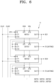
- FIG. 6 is a schematic block diagram of a driving portion in the display panel 30 according to some embodiments.
- At least portions of the first driving portion 110 A and the second driving portion 1106 may be arranged in the first corner area CR 1 , the second corner area CR 2 , the third corner area CR 3 , and the fourth corner area CR 4 corresponding to curved sides or polygonal sides.
- the first driving portion 110 A and the second driving portion 1106 may each include a plurality of normal stages NSTG and a plurality of dummy stages DSTG.
- Each of the normal stages NSTG may correspond to a pixel row provided in the display area DA.
- the number of the normal stages NSTG arranged in the first driving portion 110 A and the second driving portion 1106 may be variously changed according to the number of pixel rows.
- the normal stages NSTG may output a plurality of output signals in response to a start signal. For example, a first normal stage NSTG 1 may output a first output signal SC 1 , a second normal stage NSTG 2 may output a second output signal SC 2 , and the n-th normal stage may output the n-th output signal.
- Each of the normal stages NSTG may include an input terminal IN, a first clock terminal CT 1 , a second clock terminal CT 2 , a first power terminal VT 1 , a second power terminal VT 2 , and an output terminal OUT.
- the input terminal IN may receive, as a start signal, an external start signal STV or a carry signal output from the preceding normal stage NSTG.
- the external start signal STV may be applied to the input terminal IN of the first normal stage NSTG 1 , and from the second normal stage NSTG 2 , a carry signal (previous carry signal) output by the preceding normal stage NSTG may be applied to the input terminal IN.
- the previous carry signal may be a carry signal output by the preceding stage that is adjacent thereto.
- the first normal stage NSTG 1 may start driving in response to the external start signal STV, and the carry signal output from the first normal stage NSTG 1 may be input to the input terminal IN of the second normal stage NSTG 2 .
- a first clock signal CLK 1 or a second clock signal CLK 2 may be applied to the first clock terminal CT 1 and the second clock terminal CT 2 .
- the first clock signal CLK 1 and the second clock signal CLK 2 may be alternately applied to the normal stages NSTG.
- the first clock signal CLK 1 may be applied to the first clock terminal CT 1 of odd-numbered normal stages
- the second clock signal CLK 2 may be applied to the second clock terminal CT 2 of the odd-numbered normal stages.
- the second clock signal CLK 2 may be applied to the first clock terminal CT 1 of even-numbered normal stages
- the second clock signal CLK 2 may be applied to the second clock terminal CT 2 of the even-numbered normal stages.
- the first power terminal VT 1 may receive a first gate voltage VGH of a high voltage
- the second power terminal VT 2 may receive a second gate voltage VGL of a low voltage.
- the first gate voltage VGH and the second gate voltage VGL, as global signals, may be provided from a control unit, a power supply unit, and/or like.
- the output terminal OUT may output output signals such as the first output signal SC 1 , the second output signal SC 2 , and the like.
- the first output signal SC 1 and the second output signal SC 2 may be scan signals.
- Each output signal may be provided to a pixel P (see FIG. 3 ) through a corresponding output line, for example, the scan line SL (see FIG. 3 ).
- the dummy stages DSTG may each include the input terminal IN, the first clock terminal CT 1 , the second clock terminal CT 2 , the first power terminal VT 1 , the second power terminal VT 2 , and the output terminal OUT.
- the dummy stages DSTG are arranged to improve the uniformity of a pattern density of the first driving portion 110 A and the second driving portion 1106 , and do not output output signals.
- the output terminal OUT of the dummy stages DSTG may be floating.
- the input terminal IN, the first clock terminal CT 1 , and the second clock terminal CT 2 of each of the dummy stages DSTG may receive the first gate voltage VGH.
- the first power terminal VT 1 of each of the dummy stages DSTG may receive the first gate voltage VGH
- the second power terminal VT 2 may receive the second gate voltage VGL.
- FIG. 6 illustrates that the first normal stage NSTG 1 , a first dummy stage DSTG 1 , the second normal stage NSTG 2 , and a second dummy stage DSTG 2 are sequentially arranged
- the number of the dummy stages DSTG arranged between the normal stages NSTG neighboring each other may vary according to the arrangement position.
- one or more dummy stages DSTG may be arranged between the normal stages NSTG neighboring each other, or the normal stages NSTG may be arranged adjacent to each other without the dummy stage DSTG therebetween.
- the first driving portion 110 A may be arranged in the third corner area CR 3 and the fourth corner area CR 4 , and arranged along a first virtual line VL 1 corresponding to a curved side (or a polygonal side).
- the normal stages NSTG and the dummy stages DSTG in the first driving portion 110 A may be arranged along the first virtual line VL 1 .
- the number of dummy stages arranged for each unit length of the first virtual line VL 1 may be determined based on an angle between the first virtual line VL 1 and the first direction (x direction).
- the second driving portion 1106 may be arranged in the first corner area CR 1 and the second corner area CR 2 , along a second virtual line VL 2 corresponding to a curved side (or a polygonal side).
- the normal stages NSTG and the dummy stages DSTG in the second driving portion 1106 may be arranged along the second virtual line VL 2 .
- the number of dummy stages arranged for each unit length of the second virtual line VL 2 may be determined based on an angle formed between the second virtual line VL 2 and the first direction (x direction).
- a first length SP 1 that is the length of the first arc a 1 in the second direction (y direction), a second length SP 2 that is the length of the second arc a 2 in the second direction (y direction), and a third length SP 3 that is the length of the third arc a 3 in the second direction (y direction) may be different from one another.
- the tangent line of the first arc a 1 may form a first angle ⁇ 1 with the first direction (x direction)
- the tangent line of the second arc a 2 may form a second angle ⁇ 2 with the first direction (x direction)
- the tangent line of the third arc a 3 may form a third angle ⁇ 3 with the first direction (x direction).
- the first angle ⁇ 1 is greater than the second angle ⁇ 2
- the second angle ⁇ 2 is greater than the third angle ⁇ 3
- the first length SP 1 may be greater than the second length SP 2
- the second length SP 2 may be greater than the third length SP 3 .
- the same number of stages may be arranged in each of the first arc a 1 , the second arc a 2 , and the third arc a 3 .
- the number of pixel rows arranged in the display area DA corresponding to the first length SP 1 may be greater than the number of pixel rows arranged in the display area DA corresponding to the second length SP 2
- the number of pixel rows arranged in the display area DA corresponding to the second length SP 2 may be greater than the number of pixel rows arranged in the display area DA corresponding to the third length SP 3 .
- the number of the normal stages NSTG arranged along the first arc a 1 may be greater than the number of the normal stages NSTG arranged along the second arc a 2
- the number of the normal stages NSTG arranged along the second arc a 2 may be greater than the number of the normal stages NSTG arranged along the third arc a 3 .
- the number of the dummy stages DSTG arranged along the first arc a 1 may be less than the number of the dummy stages DSTG arranged along the second arc a 2
- the number of the dummy stages DSTG arranged along the second arc a 2 may be less than the number of the dummy stages DSTG arranged along the third arc a 3
- the normal stages NSTG and the dummy stages DSTG of the first driving portion 110 A may be arranged in the same rule.
- a first driving portion and a second driving portion include only normal stages for outputting output signals
- the timing of output signals output from the first driving portion and the second driving portion may be advanced or delayed.
- the dummy stages DSTG are arranged between the normal stages NSTG to have a uniform pattern density of each of the first driving portion 110 A and the second driving portion 1108 , and thus, the first driving portion 110 A and the second driving portion 1108 may output output signals at an accurate timing.
- FIG. 7 is a schematic plan view of the display panel 30 and the cover panel 50 according to some embodiments
- FIG. 8 is a schematic enlarged plan view of a portion of the display panel 30 according to a comparative example
- FIG. 9 is a schematic enlarged plan view of a portion of the display panel 30 according to some embodiments.
- FIG. 7 illustrates the display panel 30 and the cover panel 50 when viewed from a direction ( ⁇ z direction) perpendicular to the display panel 30 , showing that the cover panel 50 is bonded to the rear surface of the display panel 30 .
- FIGS. 8 and 9 are schematic enlarged plan views of a portion of a display panel according to a comparative example and a portion of the display panel 30 according to some embodiments, when viewed from a direction (+z direction) perpendicular to the display panel 30 (e.g., from a direction perpendicular or normal with respect to a display surface of the display panel 30 , or in a plan view), to explain the arrangement of a second alignment notch AH 2 and the first driving portion 110 A in the fourth corner area CR 4 .
- the cover panel 50 may have a shape corresponding to the display panel 30 .
- the cover panel 50 may be implemented by a film or a plate-shaped member including any one or more of a light absorption layer, a buffer member, and a heat dissipation member.
- the cover panel 50 may have the same size (or area) as or a different size (or area) from the display panel 30 .
- the size (or area) of the cover panel 50 may be less than the size (or area) of the display panel 30 . Accordingly, the edge of the cover panel 50 may be spaced apart a certain distance inwards from the edge of the display panel 30 .
- the size (or area) of the cover panel 50 may be the same as or greater than the size (or area) of the display panel 30 .
- the edge of the cover panel 50 may be located outside the first driving portion 110 A and the second driving portion 1106 . Accordingly, when viewed from the rear surface of the display panel 30 , the cover panel 50 may cover an area corresponding to the first driving portion 110 A and the second driving portion 1106 .
- the cover panel 50 may have a first alignment notch AH 1 corresponding to the first alignment mark AM 1 , the second alignment notch AH 2 corresponding to the second alignment mark AM 2 , a third alignment notch AH 3 corresponding to the third alignment mark AM 3 , and a fourth alignment notch AH 4 corresponding to the fourth alignment mark AM 4 .
- the first alignment notch AH 1 may be formed in the edge of the cover panel 50 corresponding to the first corner area CR 1
- the second alignment notch AH 2 may be formed in the edge of the cover panel 50 corresponding to the fourth corner area CR 4
- the third alignment notch AH 3 may be formed in the edge of the cover panel 50 corresponding to the second corner area CR 2
- the fourth alignment notch AH 4 may be formed in the edge of the cover panel 50 corresponding to the third corner area CR 3 .
- some of the first alignment notch AH 1 , the second alignment notch AH 2 , the third alignment notch AH 3 , and the fourth alignment notch AH 4 may be omitted.
- the first alignment mark AM 1 , the second alignment mark AM 2 , the third alignment mark AM 3 , and the fourth alignment mark AM 4 may be arranged on the front surface of the display panel 30 , and may include an opaque material.
- the first alignment mark AM 1 , the second alignment mark AM 2 , the third alignment mark AM 3 , and the fourth alignment mark AM 4 may include a metal material.
- first alignment mark AM 1 , the second alignment mark AM 2 , the third alignment mark AM 3 , and the fourth alignment mark AM 4 are substantially the same as or similar to each other, and the first alignment notch AH 1 , the second alignment notch AH 2 , the third alignment notch AH 3 , and the fourth alignment notch AH 4 are substantially the same as or similar to each other, a case in which the second alignment mark AM 2 and the second alignment notch AH 2 arranged in the fourth corner area CR 4 is mainly described below.
- a pixel circuit PC may be located on the second buffer layer 202 .
- the pixel circuit PC may include the semiconductor layer Act, a gate electrode GE, a source electrode S, a drain electrode D, and a capacitor electrode CE.
- the semiconductor layer Act may include a silicon semiconductor or an oxide semiconductor.
- the semiconductor layer Act may include a source region and a drain region, which are doped with impurities, are conductive, and are apart from each other, and a channel region arranged therebetween. The source region and the drain region may be electrically connected to the source electrode S and the drain electrode D, respectively.
Landscapes
- Engineering & Computer Science (AREA)
- Physics & Mathematics (AREA)
- Microelectronics & Electronic Packaging (AREA)
- Computer Hardware Design (AREA)
- General Physics & Mathematics (AREA)
- Theoretical Computer Science (AREA)
- Geometry (AREA)
- Devices For Indicating Variable Information By Combining Individual Elements (AREA)
- Optics & Photonics (AREA)
Abstract
Description
Claims (21)
Applications Claiming Priority (2)
| Application Number | Priority Date | Filing Date | Title |
|---|---|---|---|
| KR1020220153811A KR20240072430A (en) | 2022-11-16 | 2022-11-16 | Display panel and display apparatus including the same |
| KR10-2022-0153811 | 2022-11-16 |
Publications (2)
| Publication Number | Publication Date |
|---|---|
| US20240164195A1 US20240164195A1 (en) | 2024-05-16 |
| US12245491B2 true US12245491B2 (en) | 2025-03-04 |
Family
ID=91027901
Family Applications (1)
| Application Number | Title | Priority Date | Filing Date |
|---|---|---|---|
| US18/233,248 Active US12245491B2 (en) | 2022-11-16 | 2023-08-11 | Display panel and a display apparatus including the same |
Country Status (3)
| Country | Link |
|---|---|
| US (1) | US12245491B2 (en) |
| KR (1) | KR20240072430A (en) |
| CN (1) | CN118055640A (en) |
Citations (9)
| Publication number | Priority date | Publication date | Assignee | Title |
|---|---|---|---|---|
| US20170116923A1 (en) * | 2015-10-22 | 2017-04-27 | Samsung Display Co., Ltd. | Gate driver and display device having the same |
| KR20180030314A (en) | 2016-09-12 | 2018-03-22 | 삼성디스플레이 주식회사 | Display device |
| US20190293998A1 (en) * | 2018-03-23 | 2019-09-26 | Sharp Kabushiki Kaisha | Image display panel and image display device |
| US20200083301A1 (en) * | 2018-09-07 | 2020-03-12 | Samsung Display Co., Ltd. | Display device |
| US20210126078A1 (en) * | 2019-10-28 | 2021-04-29 | Samsung Display Co., Ltd. | Display device |
| KR20210127283A (en) | 2020-04-13 | 2021-10-22 | 삼성디스플레이 주식회사 | Display device |
| US20210378107A1 (en) | 2020-05-29 | 2021-12-02 | Samsung Display Co., Ltd. | Display device and method for fabricating display device |
| US20220045140A1 (en) * | 2020-05-09 | 2022-02-10 | Chengdu Boe Optoelectronics Technology Co., Ltd. | Display panel, method for manufacturing the same, display device and method for manufacturing the same |
| US20220165217A1 (en) | 2020-11-23 | 2022-05-26 | Samsung Display Co., Ltd. | Display device |
-
2022
- 2022-11-16 KR KR1020220153811A patent/KR20240072430A/en active Pending
-
2023
- 2023-08-11 US US18/233,248 patent/US12245491B2/en active Active
- 2023-11-01 CN CN202311444342.8A patent/CN118055640A/en active Pending
Patent Citations (15)
| Publication number | Priority date | Publication date | Assignee | Title |
|---|---|---|---|---|
| KR102429674B1 (en) | 2015-10-22 | 2022-08-08 | 삼성디스플레이 주식회사 | Gate driver and display device having the same |
| US9978314B2 (en) | 2015-10-22 | 2018-05-22 | Samsung Display Co., Ltd. | Gate driver including a plurality of normal stages and a plurality of dummy stages and display device having the same |
| US20170116923A1 (en) * | 2015-10-22 | 2017-04-27 | Samsung Display Co., Ltd. | Gate driver and display device having the same |
| KR20180030314A (en) | 2016-09-12 | 2018-03-22 | 삼성디스플레이 주식회사 | Display device |
| US10475389B2 (en) | 2016-09-12 | 2019-11-12 | Samsung Display Co., Ltd. | Display device |
| US20190293998A1 (en) * | 2018-03-23 | 2019-09-26 | Sharp Kabushiki Kaisha | Image display panel and image display device |
| US20200083301A1 (en) * | 2018-09-07 | 2020-03-12 | Samsung Display Co., Ltd. | Display device |
| US20210126078A1 (en) * | 2019-10-28 | 2021-04-29 | Samsung Display Co., Ltd. | Display device |
| US11355071B2 (en) | 2020-04-13 | 2022-06-07 | Samsung Display Co., Ltd. | Display device |
| KR20210127283A (en) | 2020-04-13 | 2021-10-22 | 삼성디스플레이 주식회사 | Display device |
| US20220045140A1 (en) * | 2020-05-09 | 2022-02-10 | Chengdu Boe Optoelectronics Technology Co., Ltd. | Display panel, method for manufacturing the same, display device and method for manufacturing the same |
| US20210378107A1 (en) | 2020-05-29 | 2021-12-02 | Samsung Display Co., Ltd. | Display device and method for fabricating display device |
| KR20210148550A (en) | 2020-05-29 | 2021-12-08 | 삼성디스플레이 주식회사 | Display device and manufacturing method of display device |
| US20220165217A1 (en) | 2020-11-23 | 2022-05-26 | Samsung Display Co., Ltd. | Display device |
| KR20220072003A (en) | 2020-11-23 | 2022-06-02 | 삼성디스플레이 주식회사 | Display device |
Also Published As
| Publication number | Publication date |
|---|---|
| KR20240072430A (en) | 2024-05-24 |
| US20240164195A1 (en) | 2024-05-16 |
| CN118055640A (en) | 2024-05-17 |
Similar Documents
| Publication | Publication Date | Title |
|---|---|---|
| US12238991B2 (en) | Display substrate comprising sub-pixels in fan-out wiring region and preparation method therefor | |
| CN113973506B (en) | Display substrate, display panel and display device | |
| CN114639343B (en) | Organic light emitting display device | |
| CN115394201B (en) | Display panel and display device | |
| US20250336360A1 (en) | Display substrate and display device | |
| US20260057848A1 (en) | Display Device Having Mux Part and Method of Driving the Same | |
| US11195861B2 (en) | Display device and method of manufacturing the same | |
| US20250017042A1 (en) | Display device | |
| CN218513458U (en) | display screen | |
| US12245491B2 (en) | Display panel and a display apparatus including the same | |
| US12424172B2 (en) | Display substrate and display apparatus | |
| CN118414044A (en) | Display device | |
| US12205538B2 (en) | Display device adjusting timing of gate signal | |
| US20240292674A1 (en) | Display device | |
| US12620359B2 (en) | Display device including one or more blocks in non-display area | |
| US20240292692A1 (en) | Display apparatus | |
| US12575190B2 (en) | Display substrate, manufacturing method thereof, and display apparatus | |
| US20240290283A1 (en) | Display device | |
| CN118574466A (en) | Display device with narrow bezel | |
| KR20250103025A (en) | Display device | |
| CN118042886A (en) | Light-emitting display device | |
| CN120548046A (en) | Display device |
Legal Events
| Date | Code | Title | Description |
|---|---|---|---|
| FEPP | Fee payment procedure |
Free format text: ENTITY STATUS SET TO UNDISCOUNTED (ORIGINAL EVENT CODE: BIG.); ENTITY STATUS OF PATENT OWNER: LARGE ENTITY |
|
| AS | Assignment |
Owner name: SAMSUNG DISPLAY CO., LTD., KOREA, REPUBLIC OF Free format text: ASSIGNMENT OF ASSIGNORS INTEREST;ASSIGNORS:JUNG, SUKYO;KIM, DAESUK;YOUN, ILGOO;REEL/FRAME:064731/0885 Effective date: 20230612 |
|
| STPP | Information on status: patent application and granting procedure in general |
Free format text: NON FINAL ACTION MAILED |
|
| STPP | Information on status: patent application and granting procedure in general |
Free format text: RESPONSE TO NON-FINAL OFFICE ACTION ENTERED AND FORWARDED TO EXAMINER |
|
| STPP | Information on status: patent application and granting procedure in general |
Free format text: FINAL REJECTION MAILED |
|
| STPP | Information on status: patent application and granting procedure in general |
Free format text: RESPONSE AFTER FINAL ACTION FORWARDED TO EXAMINER |
|
| STPP | Information on status: patent application and granting procedure in general |
Free format text: NOTICE OF ALLOWANCE MAILED -- APPLICATION RECEIVED IN OFFICE OF PUBLICATIONS |
|
| STPP | Information on status: patent application and granting procedure in general |
Free format text: PUBLICATIONS -- ISSUE FEE PAYMENT VERIFIED |
|
| STCF | Information on status: patent grant |
Free format text: PATENTED CASE |