US12243741B2 - Semiconductor structure and method for forming the same - Google Patents
Semiconductor structure and method for forming the same Download PDFInfo
- Publication number
- US12243741B2 US12243741B2 US17/674,674 US202217674674A US12243741B2 US 12243741 B2 US12243741 B2 US 12243741B2 US 202217674674 A US202217674674 A US 202217674674A US 12243741 B2 US12243741 B2 US 12243741B2
- Authority
- US
- United States
- Prior art keywords
- conductive
- conductive line
- line
- over
- conductive member
- Prior art date
- Legal status (The legal status is an assumption and is not a legal conclusion. Google has not performed a legal analysis and makes no representation as to the accuracy of the status listed.)
- Active, expires
Links
Images


Classifications
-
- H—ELECTRICITY
- H10—SEMICONDUCTOR DEVICES; ELECTRIC SOLID-STATE DEVICES NOT OTHERWISE PROVIDED FOR
- H10W—GENERIC PACKAGES, INTERCONNECTIONS, CONNECTORS OR OTHER CONSTRUCTIONAL DETAILS OF DEVICES COVERED BY CLASS H10
- H10W20/00—Interconnections in chips, wafers or substrates
- H10W20/01—Manufacture or treatment
- H10W20/031—Manufacture or treatment of conductive parts of the interconnections
- H10W20/063—Manufacture or treatment of conductive parts of the interconnections by forming conductive members before forming protective insulating material
-
- H01L21/027—
-
- H—ELECTRICITY
- H10—SEMICONDUCTOR DEVICES; ELECTRIC SOLID-STATE DEVICES NOT OTHERWISE PROVIDED FOR
- H10P—GENERIC PROCESSES OR APPARATUS FOR THE MANUFACTURE OR TREATMENT OF DEVICES COVERED BY CLASS H10
- H10P76/00—Manufacture or treatment of masks on semiconductor bodies, e.g. by lithography or photolithography
-
- H01L21/02697—
-
- H01L21/30604—
-
- H01L21/762—
-
- H01L23/49827—
-
- H01L23/522—
-
- H—ELECTRICITY
- H10—SEMICONDUCTOR DEVICES; ELECTRIC SOLID-STATE DEVICES NOT OTHERWISE PROVIDED FOR
- H10P—GENERIC PROCESSES OR APPARATUS FOR THE MANUFACTURE OR TREATMENT OF DEVICES COVERED BY CLASS H10
- H10P14/00—Formation of materials, e.g. in the shape of layers or pillars
- H10P14/40—Formation of materials, e.g. in the shape of layers or pillars of conductive or resistive materials
-
- H—ELECTRICITY
- H10—SEMICONDUCTOR DEVICES; ELECTRIC SOLID-STATE DEVICES NOT OTHERWISE PROVIDED FOR
- H10P—GENERIC PROCESSES OR APPARATUS FOR THE MANUFACTURE OR TREATMENT OF DEVICES COVERED BY CLASS H10
- H10P50/00—Etching of wafers, substrates or parts of devices
- H10P50/60—Wet etching
- H10P50/64—Wet etching of semiconductor materials
- H10P50/642—Chemical etching
-
- H—ELECTRICITY
- H10—SEMICONDUCTOR DEVICES; ELECTRIC SOLID-STATE DEVICES NOT OTHERWISE PROVIDED FOR
- H10W—GENERIC PACKAGES, INTERCONNECTIONS, CONNECTORS OR OTHER CONSTRUCTIONAL DETAILS OF DEVICES COVERED BY CLASS H10
- H10W10/00—Isolation regions in semiconductor bodies between components of integrated devices
- H10W10/01—Manufacture or treatment
- H10W10/011—Manufacture or treatment of isolation regions comprising dielectric materials
-
- H—ELECTRICITY
- H10—SEMICONDUCTOR DEVICES; ELECTRIC SOLID-STATE DEVICES NOT OTHERWISE PROVIDED FOR
- H10W—GENERIC PACKAGES, INTERCONNECTIONS, CONNECTORS OR OTHER CONSTRUCTIONAL DETAILS OF DEVICES COVERED BY CLASS H10
- H10W10/00—Isolation regions in semiconductor bodies between components of integrated devices
- H10W10/10—Isolation regions comprising dielectric materials
-
- H—ELECTRICITY
- H10—SEMICONDUCTOR DEVICES; ELECTRIC SOLID-STATE DEVICES NOT OTHERWISE PROVIDED FOR
- H10W—GENERIC PACKAGES, INTERCONNECTIONS, CONNECTORS OR OTHER CONSTRUCTIONAL DETAILS OF DEVICES COVERED BY CLASS H10
- H10W20/00—Interconnections in chips, wafers or substrates
- H10W20/01—Manufacture or treatment
- H10W20/031—Manufacture or treatment of conductive parts of the interconnections
- H10W20/063—Manufacture or treatment of conductive parts of the interconnections by forming conductive members before forming protective insulating material
- H10W20/0633—Manufacture or treatment of conductive parts of the interconnections by forming conductive members before forming protective insulating material using subtractive patterning of the conductive members
-
- H—ELECTRICITY
- H10—SEMICONDUCTOR DEVICES; ELECTRIC SOLID-STATE DEVICES NOT OTHERWISE PROVIDED FOR
- H10W—GENERIC PACKAGES, INTERCONNECTIONS, CONNECTORS OR OTHER CONSTRUCTIONAL DETAILS OF DEVICES COVERED BY CLASS H10
- H10W20/00—Interconnections in chips, wafers or substrates
- H10W20/01—Manufacture or treatment
- H10W20/031—Manufacture or treatment of conductive parts of the interconnections
- H10W20/069—Manufacture or treatment of conductive parts of the interconnections by forming self-aligned vias or self-aligned contact plugs
- H10W20/0693—Manufacture or treatment of conductive parts of the interconnections by forming self-aligned vias or self-aligned contact plugs by forming self-aligned vias
-
- H—ELECTRICITY
- H10—SEMICONDUCTOR DEVICES; ELECTRIC SOLID-STATE DEVICES NOT OTHERWISE PROVIDED FOR
- H10W—GENERIC PACKAGES, INTERCONNECTIONS, CONNECTORS OR OTHER CONSTRUCTIONAL DETAILS OF DEVICES COVERED BY CLASS H10
- H10W20/00—Interconnections in chips, wafers or substrates
- H10W20/40—Interconnections external to wafers or substrates, e.g. back-end-of-line [BEOL] metallisations or vias connecting to gate electrodes
- H10W20/41—Interconnections external to wafers or substrates, e.g. back-end-of-line [BEOL] metallisations or vias connecting to gate electrodes characterised by their conductive parts
- H10W20/42—Vias, e.g. via plugs
-
- H—ELECTRICITY
- H10—SEMICONDUCTOR DEVICES; ELECTRIC SOLID-STATE DEVICES NOT OTHERWISE PROVIDED FOR
- H10W—GENERIC PACKAGES, INTERCONNECTIONS, CONNECTORS OR OTHER CONSTRUCTIONAL DETAILS OF DEVICES COVERED BY CLASS H10
- H10W20/00—Interconnections in chips, wafers or substrates
- H10W20/40—Interconnections external to wafers or substrates, e.g. back-end-of-line [BEOL] metallisations or vias connecting to gate electrodes
- H10W20/41—Interconnections external to wafers or substrates, e.g. back-end-of-line [BEOL] metallisations or vias connecting to gate electrodes characterised by their conductive parts
- H10W20/435—Cross-sectional shapes or dispositions of interconnections
-
- H—ELECTRICITY
- H10—SEMICONDUCTOR DEVICES; ELECTRIC SOLID-STATE DEVICES NOT OTHERWISE PROVIDED FOR
- H10W—GENERIC PACKAGES, INTERCONNECTIONS, CONNECTORS OR OTHER CONSTRUCTIONAL DETAILS OF DEVICES COVERED BY CLASS H10
- H10W70/00—Package substrates; Interposers; Redistribution layers [RDL]
- H10W70/60—Insulating or insulated package substrates; Interposers; Redistribution layers
- H10W70/62—Insulating or insulated package substrates; Interposers; Redistribution layers characterised by their interconnections
- H10W70/63—Vias, e.g. via plugs
- H10W70/635—Through-vias
-
- H—ELECTRICITY
- H10—SEMICONDUCTOR DEVICES; ELECTRIC SOLID-STATE DEVICES NOT OTHERWISE PROVIDED FOR
- H10W—GENERIC PACKAGES, INTERCONNECTIONS, CONNECTORS OR OTHER CONSTRUCTIONAL DETAILS OF DEVICES COVERED BY CLASS H10
- H10W20/00—Interconnections in chips, wafers or substrates
- H10W20/01—Manufacture or treatment
- H10W20/031—Manufacture or treatment of conductive parts of the interconnections
- H10W20/056—Manufacture or treatment of conductive parts of the interconnections by filling conductive material into holes, grooves or trenches
-
- H—ELECTRICITY
- H10—SEMICONDUCTOR DEVICES; ELECTRIC SOLID-STATE DEVICES NOT OTHERWISE PROVIDED FOR
- H10W—GENERIC PACKAGES, INTERCONNECTIONS, CONNECTORS OR OTHER CONSTRUCTIONAL DETAILS OF DEVICES COVERED BY CLASS H10
- H10W20/00—Interconnections in chips, wafers or substrates
- H10W20/01—Manufacture or treatment
- H10W20/071—Manufacture or treatment of dielectric parts thereof
- H10W20/074—Manufacture or treatment of dielectric parts thereof of dielectric parts comprising thin functional dielectric layers, e.g. dielectric etch-stop, barrier, capping or liner layers
- H10W20/077—Manufacture or treatment of dielectric parts thereof of dielectric parts comprising thin functional dielectric layers, e.g. dielectric etch-stop, barrier, capping or liner layers on sidewalls or on top surfaces of conductors
Definitions
- ICs integrated circuits
- the devices are often connected by conductive traces, such as metal lines and polysilicon lines, and conductive vias to form circuits.
- the conductive traces and conductive vias are formed by photolithographic processes that include use of photoresists, photolithographic masks, specialized light sources, and various etchants.
- FIG. 1 illustrates a flowchart of a method, in accordance with some embodiments of the present disclosure.
- FIG. 2 illustrates a flowchart of a method, in accordance with some embodiments of the present disclosure.
- FIGS. 3 to 14 are perspective views illustrating exemplary operations in a method of manufacturing a semiconductor structure, in accordance with some embodiments of the present disclosure.
- FIG. 15 is a perspective view of a portion of a semiconductor structure in accordance with some embodiments of the present disclosure.
- FIG. 16 is an exploded view of a portion of a semiconductor structure in accordance with some embodiments of the present disclosure.
- FIGS. 17 to 23 are top views of a portion of a semiconductor structure in accordance with some embodiments of the present disclosure.
- FIG. 24 illustrates a flowchart of a method, in accordance with some embodiments of the present disclosure.
- FIG. 25 illustrates a flowchart of a method, in accordance with some embodiments of the present disclosure.
- FIGS. 26 to 34 are perspective views illustrating exemplary operations in a method of manufacturing a semiconductor structure, in accordance with some embodiments of the present disclosure.
- FIG. 35 is a top view of an interconnect structure in accordance with some comparative embodiments.
- FIGS. 36 and 37 are top views of a portion of a semiconductor structure in accordance with some embodiments of the present disclosure.
- first and second features are formed in direct contact
- additional features may be formed between the first and second features, such that the first and second features may not be in direct contact
- present disclosure may repeat reference numerals and/or letters in the various examples. This repetition is for the purpose of simplicity and clarity and does not in itself dictate a relationship between the various embodiments and/or configurations discussed.
- spatially relative terms such as “beneath,” “below,” “lower,” “above,” “over,” “upper,” “on” and the like, may be used herein for ease of description to describe one element or feature's relationship to another element(s) or feature(s) as illustrated in the figures.
- the spatially relative terms are intended to encompass different orientations of the device in use or operation in addition to the orientation depicted in the figures.
- the apparatus may be otherwise oriented (rotated 90 degrees or at other orientations) and the spatially relative descriptors used herein may likewise be interpreted accordingly.
- first,” “second” and “third” describe various elements, components, regions, layers and/or sections, these elements, components, regions, layers and/or sections should not be limited by these terms. These terms may be only used to distinguish one element, component, region, layer or section from another.
- the terms such as “first,” “second” and “third” when used herein do not imply a sequence or order unless clearly indicated by the context.
- the terms “substantially,” “approximately” and “about” generally mean within a value or range that can be contemplated by people having ordinary skill in the art. Alternatively, the terms “substantially,” “approximately” and “about” mean within an acceptable standard error of the mean when considered by one of ordinary skill in the art. People having ordinary skill in the art can understand that the acceptable standard error may vary according to different technologies.
- fin-type field effect transistors FinFETs
- the fins may be patterned to produce a relatively close spacing between features, for which the above disclosure is well suited.
- spacers used in forming fins of FinFETs can be processed according to the above disclosure.
- An example of such electrical connecting techniques is providing a conductive via disposed between and electrically connected to a first metal line and a second metal line over the first metal line.
- a method of manufacturing a semiconductor structure is disclosed.
- a semiconductor structure is manufactured by the method.
- an interconnect structure is manufactured by the method.
- the method includes a number of operations and the description and illustrations are not deemed as a limitation of the sequence of the operations.
- FIG. 1 illustrates a flowchart of a method 100 of manufacturing a semiconductor structure, in accordance with some embodiments.
- the method 100 includes the following steps.
- Step 101 includes forming a first conductive line over a substrate.
- Step 102 includes forming a conductive member over the first conductive line.
- Step 103 includes forming a second conductive line over the first conductive line and the conductive member.
- Step 104 includes removing a portion of the conductive member exposed by the second conductive line to form a conductive via extending between the first conductive line and the second conductive line. The formation of the second conductive line is implemented prior to the formation of the conductive via.
- FIG. 2 illustrates a flowchart of a method 200 of manufacturing a semiconductor structure, in accordance with some embodiments. Additional steps can be provided before, during, and after the steps shown in FIGS. 1 and 2 , and some of the steps described below can be replaced or eliminated in other embodiments of the method 100 and the method 200 . The order of the steps may be interchangeable.
- FIGS. 3 to 14 are schematic perspective views illustrating exemplary operations for the methods of manufacturing a semiconductor structure, such as the operations illustrated in FIGS. 1 and 2 , according to one embodiment of the present disclosure.
- the method 200 includes step 201 , which includes providing a substrate 301 .
- the substrate 301 may be processed according to applicable manufacturing processes to form integrated circuits in the substrate 301 .
- the substrate 301 is a semiconductor substrate, such as a bulk semiconductor, a semiconductor-on-insulator (SOI) substrate, or the like, and may be doped (e.g., with a p-type or an n-type dopant) or undoped.
- the substrate 301 may be a wafer, such as a silicon wafer.
- an SOI substrate is a layer of a semiconductor material formed on an insulator layer.
- the insulator layer may be, for example, a buried oxide (BOX) layer, a silicon oxide layer, or the like.
- the insulator layer is provided on a substrate, typically a silicon or glass substrate. Other substrates, such as a multi-layered or gradient substrate, may also be used.
- the semiconductor material of the substrate 301 includes silicon; germanium; a compound semiconductor including silicon carbide, gallium arsenic, gallium phosphide, indium phosphide, indium arsenide, and/or indium antimonide; an alloy semiconductor including SiGe, GaAsP, AlInAs, AlGaAs, GaInAs, GaInP, and/or GaInAsP; or a combination thereof.
- the substrate 301 is a silicon wafer.
- Devices such as transistors, diodes, capacitors, resistors, etc., may be formed in and/or on the substrate 301 and may be interconnected by metal layers formed by, for example, metallization patterns in one or more dielectric layers on the substrate 301 to form an interconnect structure.
- the method 200 includes step 202 , which includes disposing a first dielectric layer 302 over the substrate 301 .
- the first dielectric layer 302 is an inter-metal dielectric (IMD).
- the dielectric layer 302 includes low-k dielectric material.
- the dielectric constant (k value) of the low-k dielectric material may be less than 3.0, or less than about 2.5, and the dielectric material is therefore also referred to as an extreme low-k (ELK) dielectric material.
- the dielectric layer 302 includes a polymer, such as polyimide, polybenzoxazole (PBO), benzocyclobutene (BCB), ajinomoto buildup film (ABF), solder resist film (SR), or the like.
- the dielectric layer 302 is a single layer or multiple layers stacked over each other.
- the dielectric layer 302 includes a plurality of dielectric sub-layers disposed over the substrate 301 .
- the materials included in the dielectric sub-layers are the same material or different materials.
- the dielectric layer 302 is formed by suitable fabrication techniques such as spin coating, chemical vapor deposition (CVD), plasma-enhanced chemical vapor deposition (PECVD), or the like.
- the top surface 3211 of the conductive member 321 is exposed through the first dielectric layer 302 .
- a stack 307 including the first conductive line 311 and the conductive member 321 over the first conductive line 311 is formed.
- the conductive member 321 is disposed over the first conductive line 311 , and the first dielectric layer 302 surrounds the first conductive line 311 and the conductive member 321 .
- the conductive member 321 overlaps and is parallel to the first conductive line 311 .
- a width W 2 of the conductive member 321 is substantially equal to a width W 1 of the first conductive line 311 .
- the first conductive line 311 and the conductive member 321 extend along a first direction X.
- Each of the first conductive line 311 and the conductive member 321 may include conductive material such as aluminum or aluminum copper alloy.
- the first conductive line 311 is electrically coupled to the conductive member 321 .
- the first conductive line 311 is electrically coupled to respective circuits of the substrate 301 .
- the first conductive line 311 is formed on an active side of the substrate 301 .
- a shape of the first conductive line 311 from a top view perspective is not particularly limited, and may be, for example, a strip, an arc shape, or the like, and may be adjusted according to the actual needs.
- a plurality of the first conductive lines 311 are formed over the substrate 301 .
- the method 200 further includes disposing a multi-layer etching mask 341 over the first dielectric layer 302 and the conductive member 321 .
- the multi-layer etching mask 341 is formed over first dielectric layer 302 and the stack 307 .
- the multi-layer etching mask 341 is a hard mask.
- the multi-layer etching mask 341 may be formed of a metallic material, such as titanium nitride, titanium, tantalum nitride, or tantalum.
- the multi-layer etching mask 341 may be formed of metal-doped carbide (e.g., tungsten carbide) or a metalloid (e.g., silicon nitride, boron nitride or silicon carbide).
- the multi-layer etching mask 341 may be formed using CVD, PVD, atomic layer deposition (ALD), or the like.
- the multi-layer etching mask 341 is initially patterned and then the conductive member 321 is etched with the multi-layer etching mask 341 as an etching mask. The pattern of the multi-layer etching mask 341 is transferred to the conductive member 321 accordingly.
- the multi-layer etching mask 341 may include a lower layer 342 and an upper layer 343 .
- the lower layer 342 may include a cross-linked photoresist or a hard mask.
- the upper layer 343 may include a photoresist, which is exposed and developed to define an overlap area (not shown).
- the multi-layer etching mask 341 further includes a middle layer (not shown) disposed between the lower layer 342 and the upper layer 343 and including an inorganic material such as silicon oxynitride or the like.
- the method 200 includes step 204 , which includes determining an overlap area 344 of the first conductive line 311 and a second conductive line (not shown) before formation of the second conductive line (not shown).
- the overlap area 344 overlaps the first conductive line 311 .
- a width W 3 of the overlap area 344 is greater than a width of the subsequently-formed second conductive line.
- the width W 3 of the overlap area 344 is greater than the width W 2 of the conductive member 321 .
- a plurality of overlap areas 344 overlap the first conductive line 311 .
- the method 200 further includes patterning the upper layer 343 , and the remaining portion of the upper layer 343 defines the overlap area 344 . In some embodiments, a portion of the lower layer 342 is exposed after patterning the upper layer 343 . In some embodiments, the upper layer 343 is patterned by an etchant. In some embodiments, the upper layer 343 and the middle layer are patterned. In some embodiments, the method 200 further includes lithography process.
- the method 200 further includes patterning the lower layer 342 , and a remaining portion of the lower layer 342 defines the overlap area 344 .
- the lower layer 342 is patterned by an etchant.
- a portion of the conductive member 321 disposed outside of the overlap area 344 is exposed.
- the remaining portions of the lower layer 342 are then used to pattern the underlying conductive member 321 .
- the method 200 includes step 205 , which includes removing a portion of the conductive member 321 from outside of the overlap area 344 .
- the remaining conductive member 321 is disposed in the overlap area 344 .
- a portion of the first conductive line 311 disposed outside of the overlap area 344 is exposed.
- the method 200 includes disposing a dielectric layer 304 over the first conductive line 311 .
- the dielectric layer 304 is disposed outside of the overlap area 344 .
- the dielectric layer 304 is disposed adjacent to the remaining conductive member 321 , and the top surface 3021 of the first dielectric layer 302 is coplanar with a top surface of the dielectric layer 304 .
- the dielectric layer 304 includes a low-k dielectric material.
- a material included in the dielectric layer 304 and a material included in the first dielectric layer 302 are a same material or different materials.
- the method 200 includes step 206 , which includes forming the second conductive line 331 over the first conductive line 311 , the conductive member 321 and the first dielectric layer 302 , wherein a portion of the second conductive line 331 is disposed in the overlap area 344 .
- the respective process is illustrated as step 103 in the method 100 as shown in FIG. 1 .
- a portion of the conductive member 321 is exposed through the second conductive line 331 .
- the second conductive line 331 is separated from the dielectric layer 304 .
- a portion of the second conductive line 331 is disposed over the dielectric layer 304 .
- the second conductive line 331 extends along a second direction Y different from the first direction X.
- the first direction X and the second direction Y are not orthogonal to each other from a top view perspective.
- the first conductive line 311 and the second conductive line 331 are not orthogonal to each other.
- the first conductive line 311 and the second conductive line 331 are orthogonal to each other.
- a mask 345 is disposed over the second conductive line 331 .
- the mask 345 is a hard mask.
- the mask 345 overlaps and is parallel to the second conductive line 331 .
- the mask 345 may be formed by CVD, PVD, atomic layer deposition (ALD), or the like.
- the mask 345 is disposed over a conductive layer (not shown) over the remaining conductive member 321 and the first dielectric layer 302 , the mask 345 is initially patterned, and the conductive layer (not shown) is etched with the mask 345 as an etching mask.
- the pattern of the multi-layer etching mask 341 is transferred to the conductive member 321 accordingly.
- the method 200 includes step 207 , which includes removing a portion of the conductive member 321 exposed by the second conductive line 331 to form a conductive via 322 extending between the first conductive line 311 and the second conductive line 331 .
- the respective process is illustrated as step 104 in the method 100 as shown in FIG. 1 .
- the formation of the second conductive line 331 is implemented prior to the formation of the conductive via 322 .
- the portion of the conductive member 321 is removed after the formation of the second conductive line 331 .
- a portion 312 of the first conductive line 311 is exposed by the conductive via 322 .
- the method 200 further includes removing the mask 345 , and a top surface 3311 of the second conductive line 331 is exposed.
- the conductive via 322 , the first conductive line 311 and the second conductive line 331 form an interconnect structure 306 of a semiconductor structure 300 .
- the conductive via 322 , the first conductive line 311 and the second conductive line 331 can be referred to as a dual damascene structure.
- the method 200 includes step 208 , which includes disposing a second dielectric layer 305 to surround the second conductive line 331 and the conductive via 322 .
- the second dielectric layer 305 is in contact with the exposed portion 312 of the first conductive line 311 .
- a top surface of the second dielectric layer 305 is coplanar with the top surface 3311 of the second conductive line 331 .
- the top surface 3311 of the second conductive line 331 is exposed through the second dielectric layer 305 .
- the second dielectric layer 305 and the dielectric layer 304 are integral.
- a material included in the second dielectric layer 305 and a material included in the first dielectric layer 302 are a same material or different materials.
- the second dielectric layer 305 is formed by suitable fabrication techniques such as spin coating, chemical vapor deposition (CVD), plasma-enhanced chemical vapor deposition (PECVD), or the like.
- the second dielectric layer 305 is a single layer or multiple layers stacked over each other.
- FIG. 15 is a perspective view of an interconnect structure of a semiconductor structure in accordance with some embodiments of the present disclosure.
- FIG. 16 is an exploded view of an interconnect structure of a semiconductor structure in accordance with some embodiments of the present disclosure.
- the interconnect structure 306 of the semiconductor structure 300 includes the first conductive line 311 , the second conductive line 331 , and the conductive via 322 electrically connecting the first conductive line 311 to the second conductive line 331 .
- the first conductive line 311 extends along the first direction X and has a first surface 313 .
- the second conductive line 331 extends along the second direction Y different from the first direction X, disposed above the first conductive line 311 , and has a second surface 332 overlapping the first surface 313 from a top view perspective.
- the conductive via 322 extends between the first surface 313 and the second surface 332 .
- the conductive via 322 includes a first end 323 disposed within the first surface 313 , a second end 324 disposed within second surface 332 , and a cross-section 325 disposed between the first end 323 and the second end 324 .
- at least two of interior angles of the cross-section 325 are substantially unequal to 90°.
- the first surface 313 overlaps and is conformal to the second surface 332 from a top view perspective. A size and a shape of the first surface 313 are same as those of the second surface 332 . In some embodiments, the first surface 313 is a quadrilateral. In some embodiments, the first surface 313 is a parallelogram.
- the first surface 313 is in contact with the first end 323
- the second surface 332 is in contact with the second end 324 .
- the cross-section 325 of the conductive via 322 is a convex polygon, a parallelogram, a trapezoid, an oval, a round shape, or a stadium shape.
- the convex polygon includes a triangle, a quadrilateral, a pentagon, a hexagon, a heptagon, or an octagon.
- an area of the first surface 313 of the first conductive layer 311 is greater than an area of the first end 323 of the conductive via 322 .
- an area of the second surface 332 of the second conductive layer 331 is greater than an area of the second end 324 of the conductive via 322 .
- the cross-section 325 of the conductive via 322 is inwardly offset from the first surface 313 and/or the second surface 332 from a top view perspective.
- an area of a first interface 326 between the first end 323 and the first conductive line 311 is substantially equal to an area of the cross-section 325 .
- the cross-section 325 overlaps the first interface 326 from a top view perspective.
- the area of the first interface 326 is smaller than the area of the cross-section 325 .
- the area of the first interface 326 is less than an area of the first surface 313 .
- the first interface 326 is positioned within the first surface 313 from a top view perspective.
- the first interface 326 is a convex polygon, a parallelogram, a trapezoid, an oval, a round shape, or a stadium shape.
- the convex polygon includes a triangle, a quadrilateral, a pentagon, a hexagon, a heptagon, or an octagon.
- an area of a second interface 327 between the second end 324 and the second conductive line 331 is substantially equal to the area of the cross-section 325 from a top view perspective.
- the cross-section 325 is overlapped by the second interface 327 from a top view perspective.
- the area of the second interface 327 is less than the area of the cross-section 325 .
- the area of the second interface 327 is less than the area of the second surface 332 .
- the second interface 327 is positioned within the second surface 332 from a top view perspective.
- the area of the cross-section 325 is greater than the area of the second interface 327 .
- the second interface 327 is a convex polygon, a parallelogram, a trapezoid, an oval, a round shape, or a stadium shape.
- the convex polygon includes a triangle, a quadrilateral, a pentagon, a hexagon, a heptagon, or an octagon.
- FIGS. 17 to 23 are top views of an interconnect structure of a semiconductor structure in accordance with some embodiments of the present disclosure.
- a cross-section 325 of a conductive via 322 is positioned to overlap an area within a first surface 313 or a second surface 332 from a top view perspective by a predetermined inset distance D 1 .
- the predetermined inset distance D 1 is greater than 0 and less than a quarter of the width W 1 of the first conductive line 311 .
- the predetermined inset distance D 1 is greater than 0 and less than a quarter of a width W 4 of the second conductive line 331 .
- the cross-section 325 of the conductive via 322 is a stadium shape.
- the cross-section 325 of the conductive via 322 includes a first pair of sides 328 extending along a first direction X and a second pair of sides 329 extending along a second direction Y.
- a shortest distance D 2 between the first pair of sides 328 and edges of the first surface 313 is predetermined.
- a shortest distance D 3 between the second pair of sides 329 and edges of the second surface 332 is predetermined.
- the cross-section 325 of the conductive via 322 includes a fillet or a chamfer adjacent to a corner of the cross-section 325 .
- the distance D 2 is greater than 0 and less than a quarter of the width W 1 of the first conductive line 311 .
- the distance D 3 is greater than 0 and less than a quarter of the width W 4 of the second conductive line 331 .
- the distance D 2 may be same as or different from the distance D 3 .
- at least two of interior angles ⁇ of the cross-section 325 are substantially unequal to 90°. In some embodiments, all of interior angles ⁇ of the cross-section 325 are substantially unequal to 90°.
- the cross-section 325 of the conductive via 322 is substantially aligned with the first surface 313 or the second surface 332 from a top view perspective.
- a size and a shape of the cross-section 325 of the conductive via 322 are same as a size and a shape of the first surface 313 .
- the size and the shape of the cross-section 325 of the conductive via 322 are same as a size and a shape of the second surface 332 .
- the cross-section 325 of the conductive via 322 includes the first pair of sides 328 extending along the first direction X and aligned with edges of a first conductive line 311 .
- the cross-section 325 of the conductive via 322 includes the second pair of sides 329 extending along the second direction Y and aligned with edges of a second conductive line 331 .
- the distance D 2 is equal to 0.
- the distance D 3 is equal to 0.
- a width W 1 of the first conductive line 311 is different from a width W 4 of the second conductive line 331 .
- a plurality of conductive vias 322 are disposed between the first conductive line 311 and the second conductive line 331 .
- the first direction X is orthogonal to the second direction Y.
- the cross-section 325 of the conductive via 322 is a stadium shape.
- the cross-section 325 of the conductive via 322 is an oval.
- the cross-section 325 may be an oval.
- the cross-section 325 of the conductive via 322 is a pentagon. In some embodiments, the cross-section 325 of the conductive via 322 is a regular pentagon.
- FIG. 24 illustrates a flowchart of a method 400 of manufacturing a semiconductor structure, in accordance with some embodiments.
- the method 400 includes the following steps.
- Step 401 includes forming a stack including a first conductive layer and a conductive member over the first conductive layer.
- Step 402 includes patterning the first conductive layer and the conductive member to form a first conductive line and align the first conductive line with the conductive member from a top view perspective.
- Step 403 includes patterning the conductive member to form a conductive via over the first conductive layer.
- FIG. 25 illustrates a flowchart of a method 500 of manufacturing a semiconductor structure, in accordance with some embodiments. Additional steps can be provided before, during, and after the steps shown in FIGS. 24 and 25 , and some of the steps described below can be replaced or eliminated in other embodiments of the method 400 and the method 500 . The order of the steps may be interchangeable.
- FIGS. 26 to 34 are schematic views illustrating exemplary operations for the method of manufacturing a semiconductor structure, such as the operations illustrated in FIGS. 24 and 25 , according to one embodiment of the present disclosure.
- the methods 400 and 500 are configured to form the interconnect structure 306 as illustrated in FIGS. 15 and 34 .
- the method 500 includes step 501 , which includes forming a stack 307 including a first conductive layer 314 and a conductive member 321 over the first conductive layer 314 .
- the respective process is illustrated as step 401 in the method 400 as shown in FIG. 24 .
- the method 500 includes step 502 , which includes forming a mask 351 over the conductive member 321 .
- the mask 351 is formed over the stack 307 .
- the mask 351 is a hard mask.
- the mask 351 is a strip extending along the first direction X from a top view perspective.
- the mask 351 may be formed by CVD, PVD, atomic layer deposition (ALD), or the like.
- the method 500 includes step 503 , which includes patterning the first conductive layer 314 and the conductive member 321 to form a first conductive line 311 and to align the first conductive line 311 with the conductive member 321 from a top view perspective.
- the respective process is illustrated as step 402 in the method 400 as shown in FIG. 24 .
- the pattern of the mask 351 is transferred to the conductive member 321 and the first conductive layer 314 sequentially. Referring to FIGS. 25 and 28 , a portion of the conductive member 321 is removed, and a remaining conductive member 321 is aligned with the mask 351 from a top view perspective.
- the remaining conductive member 321 is a strip extending along a first direction X from a top view perspective.
- a portion of the first conductive layer 314 is exposed through the remaining conductive member 321 .
- the stack 307 includes the first conductive line 311 and the conductive member 321 . In some embodiments, the stack 307 extends along the first direction X.
- a width W 1 of the first conductive line 311 equals a width W 2 of the conductive member 321 .
- the first conductive layer 314 and the conductive member 321 are patterned simultaneously.
- the mask 351 is removed. In some embodiments, a top surface 3211 of the conductive member 321 is exposed.
- the method 500 includes step 504 , which includes patterning the conductive member 321 to form a conductive via 322 over the first conductive layer 311 .
- the respective process is illustrated as step 403 in the method 400 as shown in FIG. 24 .
- a mask 352 is disposed over the top surface 3211 of the conductive member 321 .
- the mask 352 is a hard mask.
- the mask 352 may be formed by CVD, PVD, atomic layer deposition (ALD), or the like.
- the mask 352 covers a portion of the conductive member 321 .
- a position, a shape and a size of the mask 352 are determined according to a predetermined position, a predetermined shape and a predetermined size of the subsequently-formed conductive via 322 .
- a width W 5 of the mask 352 is greater than or equal to the width W 2 of the conductive member 321 .
- the width W 5 of the mask 352 is greater than or equal to the width W 1 of the first conductive line 311 .
- a dielectric layer (not shown) surrounds the first conductive line 311 and the conductive member 321 .
- a portion of the conductive member 321 is removed, and the conductive via 322 is formed over the first conductive line 311 .
- a portion of the first conductive line 311 is exposed through the conductive via 322 from a top view perspective.
- a width W 6 of the conductive via 322 is equal to or less than the width W 1 of the first conductive line 311 .
- the width W 6 of the conductive via 322 is equal to or less than the width W 5 of the mask 352 .
- the mask 352 is removed, and a second end 324 of the conductive via 322 is exposed.
- the method 500 includes step 505 , which includes forming a second conductive line 331 over the conductive via 322 .
- the second conductive line 331 extends along a second direction Y different from the first direction X.
- the first conductive line 311 , the conductive via 322 and the second conductive line 331 are electrically connected to each other and form an interconnected structure 306 .
- a dielectric layer (not shown) surrounds the interconnected structure 306 .
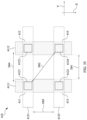
- FIG. 35 is a top view of an interconnect structure in accordance with a first comparative embodiment.
- an interconnect structure 610 includes first conductive lines 6111 and 6112 , second conductive lines 6131 and 6132 disposed over the first conductive lines 6111 and 6112 , and conductive vias 6121 , 6122 , 6123 and 6124 between the first conductive lines 6111 and 6112 and the second conductive lines 6131 and 6132 .
- the first conductive lines 6111 and 6112 and the second conductive lines 6131 and 6132 have four overlap areas 611 , 612 , 613 and 614 .
- Each of the overlap areas 611 , 612 , 613 and 614 is provided with a conductive via 6121 , 6122 , 6123 or 6124 respectively disposed therein.
- the first conductive lines 6111 and 6112 extend along a first direction X and the second conductive lines 6131 and 6132 extend along a third direction Z perpendicular to the first direction X.
- each of the conductive vias 6121 , 6122 , 6123 and 6124 is a square or a rectangle from a top view perspective, and interior angles of the conductive vias 6121 , 6122 , 6123 and 6124 from a top view perspective are equal to 90°.
- the conductive vias 6121 , 6122 , 6123 and 6124 are arranged in a quadrilateral from a top view perspective, the conductive via 6121 and the conductive via 6124 are disposed on opposite corners of the quadrilateral, and the conductive via 6122 is disposed adjacent to the conductive via 6121 .
- FIGS. 36 and 37 are top views of an interconnect structure of a semiconductor structure in accordance with some embodiments of the present disclosure.
- an interconnect structure 306 includes first conductive lines 3111 and 3112 , second conductive lines 3311 and 3312 disposed over the first conductive lines 3111 and 3112 , and conductive vias 3221 , 3222 , 3223 and 3224 between the first conductive lines 3111 and 3112 and the second conductive lines 3311 and 3312 .
- the first conductive lines 3111 and 3112 and the second conductive lines 3311 and 3312 include four overlap areas 3091 , 3092 , 3093 and 3094 .
- Each of the overlap areas 3091 , 3092 , 3093 and 3094 is provided with one of the conductive vias 3221 , 3222 , 3223 and 3224 disposed therein.
- the first conductive lines 3111 and 3112 extend along a first direction X and the second conductive lines 3311 and 3312 extend along a second direction Y different from the first direction X.
- an interconnect structure 306 includes first conductive lines 3111 and 3112 , a second conductive line 3311 disposed over the first conductive lines 3111 and 3112 , and conductive vias 3221 and 3222 between the first conductive lines 3111 and 3112 and the second conductive line 3311 .
- the first conductive lines 3111 and 3112 and the second conductive line 3311 include two overlap areas 3091 and 3092 . Each overlap area 3091 and 3092 is provided with a conductive via 3221 and 3222 disposed therein.
- the first conductive lines 3111 and 3112 extend along a first direction X and the second conductive line 3311 extends along a second direction Y different from the first direction X.
- the conductive via 3221 is adjacent to the conductive via 3222 from a top view perspective.
- each of the conductive vias 3221 and 3222 has a cross-section, and the cross-section is triangle. In some embodiments, hypotenuses of the triangles face toward each other.
- a method of manufacturing a semiconductor structure includes forming a first conductive line over a substrate; forming a conductive member over the first conductive line; and forming a second conductive line over the first conductive line and the conductive member. The method further includes removing a portion of the conductive member exposed by the second conductive line to form a conductive via extending between the first conductive line and the second conductive line, wherein the formation of the second conductive line is implemented prior to the formation of the conductive via.
- a method of manufacturing a semiconductor structure includes forming a stack including a first conductive layer and a conductive member over the first conductive layer; patterning the first conductive layer and the conductive member to form a first conductive line and to align the first conductive line with the conductive member from a top view perspective; and patterning the conductive member to form a conductive via over the first conductive layer.
- a semiconductor structure includes a first conductive line extending along a first direction and having a first surface; a second conductive line extending along a second direction different from the first direction, disposed above the first conductive line, and having a second surface overlapping the first surface; and a conductive via extending between and electrically connected to the first surface and the second surface.
- the conductive via includes a first end disposed within the first surface, a second end disposed within the second surface, and a cross-section disposed between the first end and the second end, wherein at least two of interior angles of the cross-section are substantially unequal to 90°.
Landscapes
- Chemical & Material Sciences (AREA)
- Chemical Kinetics & Catalysis (AREA)
- General Chemical & Material Sciences (AREA)
- Internal Circuitry In Semiconductor Integrated Circuit Devices (AREA)
Abstract
Description
Claims (20)
Priority Applications (2)
| Application Number | Priority Date | Filing Date | Title |
|---|---|---|---|
| US17/674,674 US12243741B2 (en) | 2022-02-17 | 2022-02-17 | Semiconductor structure and method for forming the same |
| US19/032,154 US20250218772A1 (en) | 2022-02-17 | 2025-01-20 | Semiconductor structure and method for forming the same |
Applications Claiming Priority (1)
| Application Number | Priority Date | Filing Date | Title |
|---|---|---|---|
| US17/674,674 US12243741B2 (en) | 2022-02-17 | 2022-02-17 | Semiconductor structure and method for forming the same |
Related Child Applications (1)
| Application Number | Title | Priority Date | Filing Date |
|---|---|---|---|
| US19/032,154 Division US20250218772A1 (en) | 2022-02-17 | 2025-01-20 | Semiconductor structure and method for forming the same |
Publications (2)
| Publication Number | Publication Date |
|---|---|
| US20230260786A1 US20230260786A1 (en) | 2023-08-17 |
| US12243741B2 true US12243741B2 (en) | 2025-03-04 |
Family
ID=87559036
Family Applications (2)
| Application Number | Title | Priority Date | Filing Date |
|---|---|---|---|
| US17/674,674 Active 2042-06-03 US12243741B2 (en) | 2022-02-17 | 2022-02-17 | Semiconductor structure and method for forming the same |
| US19/032,154 Pending US20250218772A1 (en) | 2022-02-17 | 2025-01-20 | Semiconductor structure and method for forming the same |
Family Applications After (1)
| Application Number | Title | Priority Date | Filing Date |
|---|---|---|---|
| US19/032,154 Pending US20250218772A1 (en) | 2022-02-17 | 2025-01-20 | Semiconductor structure and method for forming the same |
Country Status (1)
| Country | Link |
|---|---|
| US (2) | US12243741B2 (en) |
Citations (11)
| Publication number | Priority date | Publication date | Assignee | Title |
|---|---|---|---|---|
| US8796666B1 (en) | 2013-04-26 | 2014-08-05 | Taiwan Semiconductor Manufacturing Company, Ltd. | MOS devices with strain buffer layer and methods of forming the same |
| US9012132B2 (en) | 2013-01-02 | 2015-04-21 | Taiwan Semiconductor Manufacturing Company, Ltd. | Coating material and method for photolithography |
| US9028915B2 (en) | 2012-09-04 | 2015-05-12 | Taiwan Semiconductor Manufacturing Company, Ltd. | Method of forming a photoresist layer |
| US9093530B2 (en) | 2012-12-28 | 2015-07-28 | Taiwan Semiconductor Manufacturing Company, Ltd. | Fin structure of FinFET |
| US9146469B2 (en) | 2013-03-14 | 2015-09-29 | Taiwan Semiconductor Manufacturing Company, Ltd. | Middle layer composition for trilayer patterning stack |
| US9213234B2 (en) | 2012-06-01 | 2015-12-15 | Taiwan Semiconductor Manufacturing Company, Ltd. | Photosensitive material and method of lithography |
| US9223220B2 (en) | 2013-03-12 | 2015-12-29 | Taiwan Semiconductor Manufacturing Company, Ltd. | Photo resist baking in lithography process |
| US9256133B2 (en) | 2012-07-13 | 2016-02-09 | Taiwan Semiconductor Manufacturing Company, Ltd. | Apparatus and method for developing process |
| US9536759B2 (en) | 2015-05-29 | 2017-01-03 | Taiwan Semiconductor Manufacturing Co., Ltd | Baking apparatus and method |
| US9548303B2 (en) | 2014-03-13 | 2017-01-17 | Taiwan Semiconductor Manufacturing Company, Ltd. | FinFET devices with unique fin shape and the fabrication thereof |
| US20180158694A1 (en) * | 2015-06-26 | 2018-06-07 | Intel Corporation | Textile patterning for subtractively-patterned self-aligned interconnects, plugs, and vias |
-
2022
- 2022-02-17 US US17/674,674 patent/US12243741B2/en active Active
-
2025
- 2025-01-20 US US19/032,154 patent/US20250218772A1/en active Pending
Patent Citations (11)
| Publication number | Priority date | Publication date | Assignee | Title |
|---|---|---|---|---|
| US9213234B2 (en) | 2012-06-01 | 2015-12-15 | Taiwan Semiconductor Manufacturing Company, Ltd. | Photosensitive material and method of lithography |
| US9256133B2 (en) | 2012-07-13 | 2016-02-09 | Taiwan Semiconductor Manufacturing Company, Ltd. | Apparatus and method for developing process |
| US9028915B2 (en) | 2012-09-04 | 2015-05-12 | Taiwan Semiconductor Manufacturing Company, Ltd. | Method of forming a photoresist layer |
| US9093530B2 (en) | 2012-12-28 | 2015-07-28 | Taiwan Semiconductor Manufacturing Company, Ltd. | Fin structure of FinFET |
| US9012132B2 (en) | 2013-01-02 | 2015-04-21 | Taiwan Semiconductor Manufacturing Company, Ltd. | Coating material and method for photolithography |
| US9223220B2 (en) | 2013-03-12 | 2015-12-29 | Taiwan Semiconductor Manufacturing Company, Ltd. | Photo resist baking in lithography process |
| US9146469B2 (en) | 2013-03-14 | 2015-09-29 | Taiwan Semiconductor Manufacturing Company, Ltd. | Middle layer composition for trilayer patterning stack |
| US8796666B1 (en) | 2013-04-26 | 2014-08-05 | Taiwan Semiconductor Manufacturing Company, Ltd. | MOS devices with strain buffer layer and methods of forming the same |
| US9548303B2 (en) | 2014-03-13 | 2017-01-17 | Taiwan Semiconductor Manufacturing Company, Ltd. | FinFET devices with unique fin shape and the fabrication thereof |
| US9536759B2 (en) | 2015-05-29 | 2017-01-03 | Taiwan Semiconductor Manufacturing Co., Ltd | Baking apparatus and method |
| US20180158694A1 (en) * | 2015-06-26 | 2018-06-07 | Intel Corporation | Textile patterning for subtractively-patterned self-aligned interconnects, plugs, and vias |
Also Published As
| Publication number | Publication date |
|---|---|
| US20230260786A1 (en) | 2023-08-17 |
| US20250218772A1 (en) | 2025-07-03 |
Similar Documents
| Publication | Publication Date | Title |
|---|---|---|
| US12424448B2 (en) | Reduction of line wiggling | |
| KR102102735B1 (en) | Multiple patterning method | |
| US8298943B1 (en) | Self aligning via patterning | |
| CN113539799A (en) | Patterning method for semiconductor device and structure produced thereby | |
| KR20180121327A (en) | Patterning Method for Semiconductor Device and Structures resulting therefrom | |
| US20200335390A1 (en) | Method of Forming Contacts In a Semiconductor Device | |
| TWI696217B (en) | Semiconductor processing method | |
| US11121026B2 (en) | Semiconductor device and method of manufacture | |
| TW201742227A (en) | Semiconductor structure manufacturing method | |
| US20210035809A1 (en) | Self-aligned double patterning process and semiconductor structure formed using thereof | |
| US20250149447A1 (en) | Semiconductor device and manufacturing method thereof | |
| US11322393B2 (en) | Method of forming a semiconductor device | |
| US12224237B2 (en) | Method of manufacturing a via and a metal wiring for a semiconductor device | |
| US20160172297A1 (en) | Designed-based interconnect structure in semiconductor structure | |
| TWI787907B (en) | Method for manufacturing semiconductor device | |
| US12243741B2 (en) | Semiconductor structure and method for forming the same | |
| TWI793514B (en) | Semiconductor device and method of forming the same | |
| US10600860B2 (en) | Precise/designable FinFET resistor structure | |
| US11862665B2 (en) | Semiconductor structure including MIM capacitor and method of forming the same | |
| US20250096004A1 (en) | Semiconductor structures and method for manufacturing the same | |
| US20240234481A1 (en) | Semiconductor device with inductive component and method of forming | |
| US20240371803A1 (en) | Method for forming a redistribution layer structure, and chip package structure | |
| US12315815B2 (en) | Semiconductor device and manufacturing method thereof | |
| CN121038361A (en) | Semiconductor device structure and its formation method | |
| TW202347521A (en) | Semiconductor device structure and forming method thereof |
Legal Events
| Date | Code | Title | Description |
|---|---|---|---|
| FEPP | Fee payment procedure |
Free format text: ENTITY STATUS SET TO UNDISCOUNTED (ORIGINAL EVENT CODE: BIG.); ENTITY STATUS OF PATENT OWNER: LARGE ENTITY |
|
| AS | Assignment |
Owner name: TAIWAN SEMICONDUCTOR MANUFACTURING COMPANY LTD., TAIWAN Free format text: ASSIGNMENT OF ASSIGNORS INTEREST;ASSIGNORS:LI, JOHNNY CHIAHAO;CHANG`, SHIH-MING;HSIEH, KEN-HSIEN;AND OTHERS;SIGNING DATES FROM 20220624 TO 20220627;REEL/FRAME:060393/0162 |
|
| STPP | Information on status: patent application and granting procedure in general |
Free format text: RESPONSE TO NON-FINAL OFFICE ACTION ENTERED AND FORWARDED TO EXAMINER |
|
| STPP | Information on status: patent application and granting procedure in general |
Free format text: NON FINAL ACTION MAILED |
|
| STPP | Information on status: patent application and granting procedure in general |
Free format text: RESPONSE TO NON-FINAL OFFICE ACTION ENTERED AND FORWARDED TO EXAMINER |
|
| STPP | Information on status: patent application and granting procedure in general |
Free format text: FINAL REJECTION MAILED |
|
| STPP | Information on status: patent application and granting procedure in general |
Free format text: ADVISORY ACTION MAILED |
|
| STPP | Information on status: patent application and granting procedure in general |
Free format text: DOCKETED NEW CASE - READY FOR EXAMINATION |
|
| STPP | Information on status: patent application and granting procedure in general |
Free format text: NON FINAL ACTION MAILED |
|
| STPP | Information on status: patent application and granting procedure in general |
Free format text: NOTICE OF ALLOWANCE MAILED -- APPLICATION RECEIVED IN OFFICE OF PUBLICATIONS |
|
| STPP | Information on status: patent application and granting procedure in general |
Free format text: PUBLICATIONS -- ISSUE FEE PAYMENT VERIFIED |
|
| STCF | Information on status: patent grant |
Free format text: PATENTED CASE |