US12242194B2 - Resist underlayer film-forming composition comprising epoxy adduct having long-chain alkyl group - Google Patents

Resist underlayer film-forming composition comprising epoxy adduct having long-chain alkyl group Download PDF

Info

Publication number
US12242194B2
US12242194B2 US15/736,262 US201615736262A US12242194B2 US 12242194 B2 US12242194 B2 US 12242194B2 US 201615736262 A US201615736262 A US 201615736262A US 12242194 B2 US12242194 B2 US 12242194B2
Authority
US
United States
Prior art keywords
compound
group
integer
formula
epoxy
Prior art date
Legal status (The legal status is an assumption and is not a legal conclusion. Google has not performed a legal analysis and makes no representation as to the accuracy of the status listed.)
Active
Application number
US15/736,262
Other versions
US20180181001A1 (en
Inventor
Takafumi Endo
Daigo Saito
Ryo Karasawa
Rikimaru Sakamoto
Current Assignee (The listed assignees may be inaccurate. Google has not performed a legal analysis and makes no representation or warranty as to the accuracy of the list.)
Nissan Chemical Corp
Original Assignee
Nissan Chemical Corp
Priority date (The priority date is an assumption and is not a legal conclusion. Google has not performed a legal analysis and makes no representation as to the accuracy of the date listed.)
Filing date
Publication date
Application filed by Nissan Chemical Corp filed Critical Nissan Chemical Corp
Assigned to NISSAN CHEMICAL INDUSTRIES, LTD. reassignment NISSAN CHEMICAL INDUSTRIES, LTD. ASSIGNMENT OF ASSIGNORS INTEREST (SEE DOCUMENT FOR DETAILS). Assignors: ENDO, TAKAFUMI, KARASAWA, RYO, SAITO, DAIGO, SAKAMOTO, RIKIMARU
Publication of US20180181001A1 publication Critical patent/US20180181001A1/en
Application granted granted Critical
Publication of US12242194B2 publication Critical patent/US12242194B2/en
Active legal-status Critical Current
Anticipated expiration legal-status Critical

Links

Classifications

    • GPHYSICS
    • G03PHOTOGRAPHY; CINEMATOGRAPHY; ANALOGOUS TECHNIQUES USING WAVES OTHER THAN OPTICAL WAVES; ELECTROGRAPHY; HOLOGRAPHY
    • G03FPHOTOMECHANICAL PRODUCTION OF TEXTURED OR PATTERNED SURFACES, e.g. FOR PRINTING, FOR PROCESSING OF SEMICONDUCTOR DEVICES; MATERIALS THEREFOR; ORIGINALS THEREFOR; APPARATUS SPECIALLY ADAPTED THEREFOR
    • G03F7/00Photomechanical, e.g. photolithographic, production of textured or patterned surfaces, e.g. printing surfaces; Materials therefor, e.g. comprising photoresists; Apparatus specially adapted therefor
    • G03F7/004Photosensitive materials
    • G03F7/09Photosensitive materials characterised by structural details, e.g. supports, auxiliary layers
    • G03F7/11Photosensitive materials characterised by structural details, e.g. supports, auxiliary layers having cover layers or intermediate layers, e.g. subbing layers
    • CCHEMISTRY; METALLURGY
    • C08ORGANIC MACROMOLECULAR COMPOUNDS; THEIR PREPARATION OR CHEMICAL WORKING-UP; COMPOSITIONS BASED THEREON
    • C08GMACROMOLECULAR COMPOUNDS OBTAINED OTHERWISE THAN BY REACTIONS ONLY INVOLVING UNSATURATED CARBON-TO-CARBON BONDS
    • C08G59/00Polycondensates containing more than one epoxy group per molecule; Macromolecules obtained by polymerising compounds containing more than one epoxy group per molecule using curing agents or catalysts which react with the epoxy groups
    • C08G59/18Macromolecules obtained by polymerising compounds containing more than one epoxy group per molecule using curing agents or catalysts which react with the epoxy groups ; e.g. general methods of curing
    • C08G59/182Macromolecules obtained by polymerising compounds containing more than one epoxy group per molecule using curing agents or catalysts which react with the epoxy groups ; e.g. general methods of curing using pre-adducts of epoxy compounds with curing agents
    • C08G59/184Macromolecules obtained by polymerising compounds containing more than one epoxy group per molecule using curing agents or catalysts which react with the epoxy groups ; e.g. general methods of curing using pre-adducts of epoxy compounds with curing agents with amines
    • CCHEMISTRY; METALLURGY
    • C08ORGANIC MACROMOLECULAR COMPOUNDS; THEIR PREPARATION OR CHEMICAL WORKING-UP; COMPOSITIONS BASED THEREON
    • C08GMACROMOLECULAR COMPOUNDS OBTAINED OTHERWISE THAN BY REACTIONS ONLY INVOLVING UNSATURATED CARBON-TO-CARBON BONDS
    • C08G59/00Polycondensates containing more than one epoxy group per molecule; Macromolecules obtained by polymerising compounds containing more than one epoxy group per molecule using curing agents or catalysts which react with the epoxy groups
    • C08G59/18Macromolecules obtained by polymerising compounds containing more than one epoxy group per molecule using curing agents or catalysts which react with the epoxy groups ; e.g. general methods of curing
    • C08G59/182Macromolecules obtained by polymerising compounds containing more than one epoxy group per molecule using curing agents or catalysts which react with the epoxy groups ; e.g. general methods of curing using pre-adducts of epoxy compounds with curing agents
    • C08G59/186Macromolecules obtained by polymerising compounds containing more than one epoxy group per molecule using curing agents or catalysts which react with the epoxy groups ; e.g. general methods of curing using pre-adducts of epoxy compounds with curing agents with acids
    • CCHEMISTRY; METALLURGY
    • C08ORGANIC MACROMOLECULAR COMPOUNDS; THEIR PREPARATION OR CHEMICAL WORKING-UP; COMPOSITIONS BASED THEREON
    • C08GMACROMOLECULAR COMPOUNDS OBTAINED OTHERWISE THAN BY REACTIONS ONLY INVOLVING UNSATURATED CARBON-TO-CARBON BONDS
    • C08G59/00Polycondensates containing more than one epoxy group per molecule; Macromolecules obtained by polymerising compounds containing more than one epoxy group per molecule using curing agents or catalysts which react with the epoxy groups
    • C08G59/18Macromolecules obtained by polymerising compounds containing more than one epoxy group per molecule using curing agents or catalysts which react with the epoxy groups ; e.g. general methods of curing
    • C08G59/20Macromolecules obtained by polymerising compounds containing more than one epoxy group per molecule using curing agents or catalysts which react with the epoxy groups ; e.g. general methods of curing characterised by the epoxy compounds used
    • C08G59/22Di-epoxy compounds
    • CCHEMISTRY; METALLURGY
    • C09DYES; PAINTS; POLISHES; NATURAL RESINS; ADHESIVES; COMPOSITIONS NOT OTHERWISE PROVIDED FOR; APPLICATIONS OF MATERIALS NOT OTHERWISE PROVIDED FOR
    • C09DCOATING COMPOSITIONS, e.g. PAINTS, VARNISHES OR LACQUERS; FILLING PASTES; CHEMICAL PAINT OR INK REMOVERS; INKS; CORRECTING FLUIDS; WOODSTAINS; PASTES OR SOLIDS FOR COLOURING OR PRINTING; USE OF MATERIALS THEREFOR
    • C09D163/00Coating compositions based on epoxy resins; Coating compositions based on derivatives of epoxy resins
    • CCHEMISTRY; METALLURGY
    • C09DYES; PAINTS; POLISHES; NATURAL RESINS; ADHESIVES; COMPOSITIONS NOT OTHERWISE PROVIDED FOR; APPLICATIONS OF MATERIALS NOT OTHERWISE PROVIDED FOR
    • C09DCOATING COMPOSITIONS, e.g. PAINTS, VARNISHES OR LACQUERS; FILLING PASTES; CHEMICAL PAINT OR INK REMOVERS; INKS; CORRECTING FLUIDS; WOODSTAINS; PASTES OR SOLIDS FOR COLOURING OR PRINTING; USE OF MATERIALS THEREFOR
    • C09D5/00Coating compositions, e.g. paints, varnishes or lacquers, characterised by their physical nature or the effects produced; Filling pastes
    • C09D5/006Anti-reflective coatings
    • GPHYSICS
    • G03PHOTOGRAPHY; CINEMATOGRAPHY; ANALOGOUS TECHNIQUES USING WAVES OTHER THAN OPTICAL WAVES; ELECTROGRAPHY; HOLOGRAPHY
    • G03FPHOTOMECHANICAL PRODUCTION OF TEXTURED OR PATTERNED SURFACES, e.g. FOR PRINTING, FOR PROCESSING OF SEMICONDUCTOR DEVICES; MATERIALS THEREFOR; ORIGINALS THEREFOR; APPARATUS SPECIALLY ADAPTED THEREFOR
    • G03F7/00Photomechanical, e.g. photolithographic, production of textured or patterned surfaces, e.g. printing surfaces; Materials therefor, e.g. comprising photoresists; Apparatus specially adapted therefor
    • G03F7/004Photosensitive materials
    • G03F7/0045Photosensitive materials with organic non-macromolecular light-sensitive compounds not otherwise provided for, e.g. dissolution inhibitors
    • GPHYSICS
    • G03PHOTOGRAPHY; CINEMATOGRAPHY; ANALOGOUS TECHNIQUES USING WAVES OTHER THAN OPTICAL WAVES; ELECTROGRAPHY; HOLOGRAPHY
    • G03FPHOTOMECHANICAL PRODUCTION OF TEXTURED OR PATTERNED SURFACES, e.g. FOR PRINTING, FOR PROCESSING OF SEMICONDUCTOR DEVICES; MATERIALS THEREFOR; ORIGINALS THEREFOR; APPARATUS SPECIALLY ADAPTED THEREFOR
    • G03F7/00Photomechanical, e.g. photolithographic, production of textured or patterned surfaces, e.g. printing surfaces; Materials therefor, e.g. comprising photoresists; Apparatus specially adapted therefor
    • G03F7/004Photosensitive materials
    • G03F7/09Photosensitive materials characterised by structural details, e.g. supports, auxiliary layers
    • G03F7/091Photosensitive materials characterised by structural details, e.g. supports, auxiliary layers characterised by antireflection means or light filtering or absorbing means, e.g. anti-halation, contrast enhancement
    • GPHYSICS
    • G03PHOTOGRAPHY; CINEMATOGRAPHY; ANALOGOUS TECHNIQUES USING WAVES OTHER THAN OPTICAL WAVES; ELECTROGRAPHY; HOLOGRAPHY
    • G03FPHOTOMECHANICAL PRODUCTION OF TEXTURED OR PATTERNED SURFACES, e.g. FOR PRINTING, FOR PROCESSING OF SEMICONDUCTOR DEVICES; MATERIALS THEREFOR; ORIGINALS THEREFOR; APPARATUS SPECIALLY ADAPTED THEREFOR
    • G03F7/00Photomechanical, e.g. photolithographic, production of textured or patterned surfaces, e.g. printing surfaces; Materials therefor, e.g. comprising photoresists; Apparatus specially adapted therefor
    • G03F7/004Photosensitive materials
    • G03F7/09Photosensitive materials characterised by structural details, e.g. supports, auxiliary layers
    • G03F7/094Multilayer resist systems, e.g. planarising layers
    • GPHYSICS
    • G03PHOTOGRAPHY; CINEMATOGRAPHY; ANALOGOUS TECHNIQUES USING WAVES OTHER THAN OPTICAL WAVES; ELECTROGRAPHY; HOLOGRAPHY
    • G03FPHOTOMECHANICAL PRODUCTION OF TEXTURED OR PATTERNED SURFACES, e.g. FOR PRINTING, FOR PROCESSING OF SEMICONDUCTOR DEVICES; MATERIALS THEREFOR; ORIGINALS THEREFOR; APPARATUS SPECIALLY ADAPTED THEREFOR
    • G03F7/00Photomechanical, e.g. photolithographic, production of textured or patterned surfaces, e.g. printing surfaces; Materials therefor, e.g. comprising photoresists; Apparatus specially adapted therefor
    • G03F7/16Coating processes; Apparatus therefor
    • GPHYSICS
    • G03PHOTOGRAPHY; CINEMATOGRAPHY; ANALOGOUS TECHNIQUES USING WAVES OTHER THAN OPTICAL WAVES; ELECTROGRAPHY; HOLOGRAPHY
    • G03FPHOTOMECHANICAL PRODUCTION OF TEXTURED OR PATTERNED SURFACES, e.g. FOR PRINTING, FOR PROCESSING OF SEMICONDUCTOR DEVICES; MATERIALS THEREFOR; ORIGINALS THEREFOR; APPARATUS SPECIALLY ADAPTED THEREFOR
    • G03F7/00Photomechanical, e.g. photolithographic, production of textured or patterned surfaces, e.g. printing surfaces; Materials therefor, e.g. comprising photoresists; Apparatus specially adapted therefor
    • G03F7/20Exposure; Apparatus therefor
    • G03F7/2002Exposure; Apparatus therefor with visible light or UV light, through an original having an opaque pattern on a transparent support, e.g. film printing, projection printing; by reflection of visible or UV light from an original such as a printed image
    • GPHYSICS
    • G03PHOTOGRAPHY; CINEMATOGRAPHY; ANALOGOUS TECHNIQUES USING WAVES OTHER THAN OPTICAL WAVES; ELECTROGRAPHY; HOLOGRAPHY
    • G03FPHOTOMECHANICAL PRODUCTION OF TEXTURED OR PATTERNED SURFACES, e.g. FOR PRINTING, FOR PROCESSING OF SEMICONDUCTOR DEVICES; MATERIALS THEREFOR; ORIGINALS THEREFOR; APPARATUS SPECIALLY ADAPTED THEREFOR
    • G03F7/00Photomechanical, e.g. photolithographic, production of textured or patterned surfaces, e.g. printing surfaces; Materials therefor, e.g. comprising photoresists; Apparatus specially adapted therefor
    • G03F7/20Exposure; Apparatus therefor
    • G03F7/2037Exposure with X-ray radiation or corpuscular radiation, through a mask with a pattern opaque to that radiation
    • GPHYSICS
    • G03PHOTOGRAPHY; CINEMATOGRAPHY; ANALOGOUS TECHNIQUES USING WAVES OTHER THAN OPTICAL WAVES; ELECTROGRAPHY; HOLOGRAPHY
    • G03FPHOTOMECHANICAL PRODUCTION OF TEXTURED OR PATTERNED SURFACES, e.g. FOR PRINTING, FOR PROCESSING OF SEMICONDUCTOR DEVICES; MATERIALS THEREFOR; ORIGINALS THEREFOR; APPARATUS SPECIALLY ADAPTED THEREFOR
    • G03F7/00Photomechanical, e.g. photolithographic, production of textured or patterned surfaces, e.g. printing surfaces; Materials therefor, e.g. comprising photoresists; Apparatus specially adapted therefor
    • G03F7/26Processing photosensitive materials; Apparatus therefor
    • HELECTRICITY
    • H01ELECTRIC ELEMENTS
    • H01LSEMICONDUCTOR DEVICES NOT COVERED BY CLASS H10
    • H01L21/00Processes or apparatus adapted for the manufacture or treatment of semiconductor or solid state devices or of parts thereof
    • H01L21/02Manufacture or treatment of semiconductor devices or of parts thereof
    • H01L21/04Manufacture or treatment of semiconductor devices or of parts thereof the devices having potential barriers, e.g. a PN junction, depletion layer or carrier concentration layer
    • H01L21/18Manufacture or treatment of semiconductor devices or of parts thereof the devices having potential barriers, e.g. a PN junction, depletion layer or carrier concentration layer the devices having semiconductor bodies comprising elements of Group IV of the Periodic Table or AIIIBV compounds with or without impurities, e.g. doping materials
    • H01L21/30Treatment of semiconductor bodies using processes or apparatus not provided for in groups H01L21/20 - H01L21/26
    • H01L21/302Treatment of semiconductor bodies using processes or apparatus not provided for in groups H01L21/20 - H01L21/26 to change their surface-physical characteristics or shape, e.g. etching, polishing, cutting
    • H01L21/306Chemical or electrical treatment, e.g. electrolytic etching
    • H01L21/308Chemical or electrical treatment, e.g. electrolytic etching using masks
    • H01L21/3081Chemical or electrical treatment, e.g. electrolytic etching using masks characterised by their composition, e.g. multilayer masks, materials
    • HELECTRICITY
    • H01ELECTRIC ELEMENTS
    • H01LSEMICONDUCTOR DEVICES NOT COVERED BY CLASS H10
    • H01L21/00Processes or apparatus adapted for the manufacture or treatment of semiconductor or solid state devices or of parts thereof
    • H01L21/02Manufacture or treatment of semiconductor devices or of parts thereof
    • H01L21/04Manufacture or treatment of semiconductor devices or of parts thereof the devices having potential barriers, e.g. a PN junction, depletion layer or carrier concentration layer
    • H01L21/18Manufacture or treatment of semiconductor devices or of parts thereof the devices having potential barriers, e.g. a PN junction, depletion layer or carrier concentration layer the devices having semiconductor bodies comprising elements of Group IV of the Periodic Table or AIIIBV compounds with or without impurities, e.g. doping materials
    • H01L21/30Treatment of semiconductor bodies using processes or apparatus not provided for in groups H01L21/20 - H01L21/26
    • H01L21/302Treatment of semiconductor bodies using processes or apparatus not provided for in groups H01L21/20 - H01L21/26 to change their surface-physical characteristics or shape, e.g. etching, polishing, cutting
    • H01L21/306Chemical or electrical treatment, e.g. electrolytic etching
    • H01L21/308Chemical or electrical treatment, e.g. electrolytic etching using masks
    • H01L21/3083Chemical or electrical treatment, e.g. electrolytic etching using masks characterised by their size, orientation, disposition, behaviour, shape, in horizontal or vertical plane
    • H01L21/3086Chemical or electrical treatment, e.g. electrolytic etching using masks characterised by their size, orientation, disposition, behaviour, shape, in horizontal or vertical plane characterised by the process involved to create the mask, e.g. lift-off masks, sidewalls, or to modify the mask, e.g. pre-treatment, post-treatment
    • H10P50/692
    • H10P50/695
    • H10P76/00

Definitions

  • the present invention relates to a resist underlayer film-forming composition for formation of a flattened film on a stepped substrate, and a method for producing a laminated substrate that is flattened using a resist underlayer film formed from the composition.
  • the microprocessing is a processing method in which a thin film of the photoresist composition is formed on a substrate to be processed such as a silicon wafer, irradiated with active light such as ultraviolet light through a mask pattern that has a pattern of the semiconductor device, and developed to obtain a photoresist pattern, and the substrate to be processed such as a silicon wafer is etched using the photoresist pattern as a protective film.
  • the depth of focus decreases with a decrease in wavelength of exposure light. Therefore, it is important that the flattening properties of a film to be formed on a substrate are improved for formation of a desired resist pattern with precision. Specifically, a resist underlayer film capable of forming a stepless and flat coating film on a substrate is required to produce a semiconductor device having a finer design rule.
  • a resist underlayer film-forming composition containing a crosslinkable compound having a C 2-10 alkoxymethyl group or a C 1-10 alkyl group is disclosed (see Patent Document 1).
  • a crosslinkable compound having a C 2-10 alkoxymethyl group or a C 1-10 alkyl group is disclosed (see Patent Document 1).
  • a resist underlayer film-forming composition using a polymer containing in a main chain a structure obtained by reacting an epoxy compound having a C 1-10 alkylene group with a compound reactive to the epoxy compound is disclosed (see Patent Document 2).
  • the resist underlayer film-forming composition having thermosetting properties contains a polymer having a thermal crosslinking-forming functional group such as a hydroxyl group, a crosslinker, and an acid catalyst (acid generator).
  • An object of the present invention is to improve the filling properties of the pattern during baking by enhancing the thermal reflow properties of the polymer.
  • a long-chain alkyl group capable of decreasing the glass transition temperature of the polymer is introduced.
  • a resist underlayer film-forming composition in which a decrease in viscosity is sufficiently expressed before a crosslinking reaction during baking starts and a coating film having high flattening properties is formed on a substrate is provided.
  • a first aspect of the present invention is a resist underlayer film-forming composition
  • an epoxy adduct (C) obtained by reacting an epoxy group-containing compound (A) with an epoxy adduct-forming compound (B), wherein one or both of the epoxy group-containing compound (A) and the epoxy adduct-forming compound (B) contain an optionally branched alkyl group having a carbon atom number of three or more.
  • a second aspect of the present invention is the resist underlayer film-forming composition according to the first aspect, wherein the epoxy adduct-forming compound (B) is at least one compound selected from the group consisting of carboxylic acid (B1), carboxylic anhydride (B2), a phenol compound (B3), a hydroxyl group-containing compound (B4), a thiol compound (B5), an amino compound (B6), and an imide compound (B7).
  • the epoxy adduct-forming compound (B) is at least one compound selected from the group consisting of carboxylic acid (B1), carboxylic anhydride (B2), a phenol compound (B3), a hydroxyl group-containing compound (B4), a thiol compound (B5), an amino compound (B6), and an imide compound (B7).
  • a third aspect of the present invention is the resist underlayer film-forming composition according to the first or second aspect, wherein the optionally branched alkyl group having a carbon atom number of three or more is contained in the epoxy adduct-forming compound (B).
  • a fourth aspect of the present invention is the resist underlayer film-forming composition according to any one of the first to third aspects, wherein the optionally branched alkyl group having a carbon atom number of three or more is a C 3-19 alkyl group.
  • a fifth aspect of the present invention is the resist underlayer film-forming composition according to any one of the first to fourth aspects, wherein the epoxy group-containing compound (A) is a compound having a structure of formula (1):
  • Ep is formula 1A or 1B:
  • n1 is an integer of 1
  • n2 and n3 are each an integer of 0 or 1
  • n4 is an integer of 1 to 100]
  • a polymer having a partial structure of the compound
  • a sixth aspect of the present invention is the resist underlayer film-forming composition according to any one of the second to fourth aspects, wherein the carboxylic acid (B1) is a compound of formula (2):
  • R 1 is an optionally branched alkyl group having a carbon atom number of 3 to 19
  • Ar 1 is a C 6-40 arylene group optionally having a substituent
  • n5 and n6 are each an integer of 0 or 1
  • n7 is an integer of 1
  • n8 is an integer of 1 or 2).
  • a seventh aspect of the present invention is the resist underlayer film-forming composition according to any one of the second to fourth aspects, wherein the carboxylic anhydride (B2) is a compound of formula (3):
  • Aa is an acid anhydride group
  • R 2 is an optionally branched alkyl group having a carbon atom number of 3 to 19
  • Ar 2 is a C 6-40 arylene group optionally having a substituent
  • n9 and n10 are each an integer of 0 or 1
  • n11 is an integer of 1).
  • An eighth aspect of the present invention is the resist underlayer film-forming composition according to any one of the second to fourth aspects, wherein the phenol compound (B3) is a compound of formula (4):
  • R 3 is an optionally branched alkyl group having a carbon atom number of 3 to 19
  • Ar 3 is a C 6-40 arylene group optionally having a substituent
  • n12 is an integer of 0 or 1
  • n13 is an integer of 1
  • n14 is an integer of 1
  • n15 is an integer of 1 to 3
  • a ninth aspect of the present invention is the resist underlayer film-forming composition according to any one of the second to fourth aspects, wherein the hydroxyl group-containing compound (B4) is a compound of formula (5):
  • R 4 is an optionally branched alkyl group having a carbon atom number of 3 to 19, n16 is an integer of 1 to 3, and n17 is an integer of 1).
  • a tenth aspect of the present invention is the resist underlayer film-forming composition according to any one of the second to fourth aspects, wherein the thiol compound (B5) is a compound of formula (6):
  • R 5 is an optionally branched alkyl group having a carbon atom number of 3 to 19
  • Ar 4 is a C 6-40 arylene group optionally having a substituent
  • n18 and n19 are each an integer of 0 or 1
  • n20 is an integer of 1
  • n21 is an integer of 1 to 3
  • An eleventh aspect of the present invention is the resist underlayer film-forming composition according to any one of the second to fourth aspects, wherein the amino compound (B6) is a compound of formula (7):
  • R 6 is an optionally branched alkyl group having a carbon atom number of 3 to 19
  • Ar 5 is a C 6-40 arylene group optionally having a substituent
  • n22 and n23 are each an integer of 0 or 1
  • n24 is an integer of 1
  • n25 is an integer of 1 to 3
  • a twelfth aspect of the present invention is the resist underlayer film-forming composition according to any one of the second to fourth aspects, wherein the imide compound (B7) is a compound of formula (8):
  • n26 and n27 are each an integer of 0 or 1
  • n28 is an integer of 1
  • n29 is an integer of 1).
  • a thirteenth aspect of the present invention is the resist underlayer film-forming composition according to any one of the first to twelfth aspects, wherein the epoxy adduct (C) is formed by reacting an epoxy group-containing compound (A) having at least two epoxy groups with an epoxy adduct-forming compound (B) having an epoxy addition reactive group.
  • a fourteenth aspect of the present invention is the resist underlayer film-forming composition according to any one of the first to thirteenth aspects, further comprising a crosslinker.
  • a fifteenth aspect of the present invention is the resist underlayer film-forming composition according to any one of the first to fourteenth aspects, further comprising an acid or an acid generator.
  • a sixteenth aspect of the present invention is a resist underlayer film formed on a semiconductor substrate from a cured product of the resist underlayer film-forming composition according to any one of the first to fifteenth aspects.
  • a seventeenth aspect of the present invention is a method for producing a semiconductor device comprising steps of forming an underlayer film on a semiconductor substrate from the resist underlayer film-forming composition according to any one of the first to fifteenth aspects, forming a resist film on the underlayer film, forming a resist pattern by irradiation with light or an electron beam and development, etching the underlayer film through the formed resist pattern, and processing the semiconductor substrate through the patterned underlayer film.
  • An eighteenth aspect of the present invention is a method for producing a semiconductor device comprising steps of forming an underlayer film on a semiconductor substrate from the resist underlayer film-forming composition according to any one of the first to fifteenth aspects, forming a hard mask on the underlayer film, forming a resist film on the hard mask, forming a resist pattern by irradiation with light or an electron beam and development, etching the hard mask through the formed resist pattern, etching the underlayer film through the patterned hard mask, and processing the semiconductor substrate through the patterned underlayer film.
  • the thermal reflow properties during baking are enhanced by imparting a long-chain alkyl group capable of decreasing the glass transition temperature (Tg) of a polymer to a skeleton of a main resin in the resist underlayer film-forming composition.
  • Tg glass transition temperature
  • the filling properties of a pattern on the substrate can be improved due to high thermal reflow properties of the polymer.
  • a flat film can be formed on the substrate regardless of an open area (unpatterned area) and a pattern area of DENSE (dense) and ISO (coarse) on the substrate.
  • the resist underlayer film-forming composition of the present invention satisfies both the filling properties of the pattern and the flattening properties after filling, and an excellent flattened film can be formed.
  • the resist underlayer film-forming composition of the present invention has an appropriate anti-reflective effect and a dry etching rate higher than that of a resist film. Therefore, the substrate can be processed.
  • the present invention is a resist underlayer film-forming composition
  • an epoxy adduct (C) obtained by reacting an epoxy group-containing compound (A) with an epoxy adduct-forming compound (B), wherein one or both of the epoxy group-containing compound (A) and the epoxy adduct-forming compound (B) contain an optionally branched alkyl group having a carbon atom number of three or more.
  • the resist underlayer film-forming composition for lithography contains the above-described resin and a solvent.
  • the composition can contain a crosslinker, an acid, an acid generator, a surfactant, or the like, if necessary.
  • the solid content of the composition is 0.1 to 70% by mass, or 0.1 to 60% by mass.
  • the solid content is a content ratio of all components other than the solvent in the resist underlayer film-forming composition.
  • the epoxy adduct (C) can be contained in an amount of 1 to 100% by mass, 1 to 99.9% by mass, 50 to 99.9% by mass, 50 to 95% by mass, or 50 to 90% by mass, in the solid content.
  • an optionally branched alkyl group having a carbon atom number of 3 or more in the present invention for example, an optionally branched alkyl group having a carbon atom number of 3 to 19 can be used.
  • hydrogen atoms may be partially substituted with a hydroxyl group, a nitro group, a cyano group, or a halogen atom (fluorine, chlorine, bromine, iodine).
  • epoxy group-containing compound (A) used in the present invention a compound having a structure of formula (1) or a polymer having a partial structure thereof can be used.
  • P A is a unit structure constituting a compound or a polymer that contains an aliphatic or aromatic hydrocarbon optionally containing an oxygen atom or a nitrogen atom, or a combination thereof.
  • P A may have a hydroxyl group as a substituent, or an ether structure, a ketone structure, or an ester structure in a main chain structure.
  • Ep is a group of formula (1A) or (1B).
  • a dotted line is a bond.
  • n1 is an integer of 1
  • n2 and n3 are each an integer of 0 or 1
  • n4 is an integer of 1 to 100.
  • n4 is 1 to 10, 1 to 4, or 2 to 4.
  • n4 can fall within a range of 1 to 100 or 2 to 100, and n4 can be at least 2.
  • Examples of the epoxy group-containing compound (A) include an epoxy group-containing benzene or epoxy group-containing benzene fused cyclic compound, an epoxy group-containing aliphatic polyether, an epoxy group-containing novolak polymer, a polyether of epoxy group-containing alicyclic hydrocarbon, and an epoxy group-containing polyester. Examples thereof include as follows.
  • the compound of formula (1-1) is trade name EPOLEAD GT401 available from Daicel Corporation.
  • a, b, c, and d are each 0 or 1, and a+b+c+d is 1.
  • the compound of formula (1-2) can be obtained as trade name YH-434L available from NIPPON STEEL & SUMIKIN CHEMICAL CO., LTD.
  • the compound of formula (1-3) can be obtained as trade name EX-411 available from Nagase ChemteX Corporation.
  • the compound of formula (1-4) can be obtained as trade name EX-521 available from Nagase ChemteX Corporation.
  • the compound of formula (1-5) can be obtained as trade name EX-611 available from Nagase ChemteX Corporation.
  • the compound of formula (1-6) can be obtained as trade name EPICLON HP-4770 available from DIC Corporation.
  • the compound of formula (1-7) can be obtained as trade name EPICLON HP-4700 available from DIC Corporation.
  • the compound of formula (1-8) can be obtained as trade name TEP-G available from Asahi Organic Chemicals Industry Co., Ltd.
  • the compound of formula (1-9) can be obtained as trade name EHPE-3150 available from Daicel Corporation.
  • the compound of formula (1-10) can be obtained as trade name EPPN-201 available from NIPPON KAYAKU Co., Ltd.
  • the compound of formula (1-11) can be obtained as trade name ECN-1229 available from Asahi Kasei Epoxy Co., Ltd.
  • the compound of formula (1-12) can be obtained as trade name EPPN-501H available from NIPPON KAYAKU Co., Ltd.
  • the compound of formula (1-13) can be obtained as trade name NC-2000L available from NIPPON KAYAKU Co., Ltd.
  • the compound of formula (1-14) can be obtained as trade name NC-3000L available from NIPPON KAYAKU Co., Ltd.
  • the compound of formula (1-15) can be obtained as trade name NC-7000L available from NIPPON KAYAKU Co., Ltd.
  • the compound of formula (1-16) can be obtained as trade name NC-7300L available from NIPPON KAYAKU Co., Ltd.
  • the compound of formula (1-17) can be obtained as trade name EPICLON HP-5000 available from DIC Corporation.
  • epoxy resins can be obtained as trade name EPICLON HP-6000 and the like available from DIC Corporation.
  • epoxy adduct-forming compound (B) used in the present invention at least one compound selected from the group consisting of carboxylic acid (B1), carboxylic anhydride (B2), a phenol compound (B3), a hydroxyl group-containing compound (B4), a thiol compound (B5), an amino compound (B6), and an imide compound (B7) can be used.
  • the epoxy adduct-forming compound (B) the carboxylic acid (B1), the phenol compound (B3), or a mixture thereof can be used.
  • the epoxy adduct-forming compound (B) can contain an optionally branched alkyl group having a carbon atom number of three or more, preferably a carbon atom number of 3 to 19.
  • R 1 is an optionally branched alkyl group having a carbon atom number of 3 to 19
  • Ar 1 is a C 6-40 arylene group optionally having a substituent
  • n5 and n6 are each an integer of 0 or 1
  • n7 is an integer of 1
  • n8 is an integer of 1 or 2.
  • an integer of 1 can be selected, and in this case, the number of carboxylic acid group in the molecule is one.
  • Aa is an acid anhydride group
  • R 2 is an optionally branched alkyl group having a carbon atom number of 3 to 19
  • Ar 2 is a C 6-40 arylene group optionally having a substituent
  • n9 and n10 are each an integer of 0 or 1
  • n11 is an integer of 1.
  • Examples of the arylene group can be those exemplified as described above.
  • the carboxylic anhydride (B2) is a compound having one carboxylic anhydride group in the molecule.
  • a compound of formula (6) can be used as the thiol compound (B5).
  • R 5 is an optionally branched alkyl group having a carbon atom number of 3 to 19
  • Ar 4 is a C 6-40 arylene group optionally having a substituent
  • n18 and n19 are each an integer of 0 or 1
  • n20 is an integer of 1
  • n21 is an integer of 1 to 3.
  • Examples of the arylene group can be those exemplified as described above.
  • n21 an integer of 1 can be selected, and in this case, the number of thiol group in the molecule is one.
  • an epoxy adduct (C) formed by reacting the epoxy group-containing compound (A) having at least two epoxy groups with the epoxy adduct-forming compound (B) having an epoxy addition reactive group can be used as the epoxy adduct (C).
  • R 11 , R 12 , R 13 , and R 14 described above are a hydrogen atom or a C 1-10 alkyl group, and as the alkyl group, the aforementioned examples can be used.
  • Examples of the compound of formula (3A) and the polymer and oligomer of formula (3B) include as follows.
  • the amount of crosslinker to be added varies depending on a coating solvent to be used, an underlying substrate to be used, a solution viscosity to be required, and a film form to be required.
  • the amount is 0.001 to 80% by mass, preferably 0.01 to 50% by mass, and further preferably 0.05 to 40% by mass, relative to the total solid content.
  • the crosslinker may cause a crosslinking reaction due to self-condensation. However, when the polymer in the present invention has a crosslinkable substituent, the crosslinker may cause a crosslinking reaction with the crosslinkable substituent.
  • an acid and/or an acid generator can be added as a catalyst for promoting the crosslinking reaction.
  • an acidic compound such as p-toluenesulfonic acid, trifluoromethanesulfonic acid, pyridinium p-toluenesulfonic acid, salicylic acid, 5-sulfosalicylic acid, 4-phenolsulfonic acid, camphorsulfonic acid, 4-chlorobenzenesulfonic acid, benzenedisulfonic acid, 1-naphthalenesulfonic acid, citric acid, benzoic acid, hydroxybenzoic acid, or naphthalenecarboxylic acid, and/or a thermal acid generator such as 2,4,4,6-tetrabromocyclohexadienone, benzoin tosylate, 2-nitrobenzyl tosylate, or another organic alkyl sulfonate can be mixed.
  • the amount of the catalyst to be mixed is 0.0001
  • the resist underlayer film-forming composition for lithography of the present invention can contain a photoacid generator in order to coincide the acidity of a photoresist covering an upper layer in a lithography process.
  • a photoacid generator include onium salt-based photoacid generators such as bis(4-t-butylphenyl)iodonium trifluoromethanesulfonate and triphenylsulfonium trifluoromethanesulfonate, halogen-containing compound-based photoacid generators such as phenyl-bis(trichloromethyl)-s-triazine, and sulfonic acid-based photoacid generators such as benzoin tosylate and N-hydroxysuccinimide trifluoromethanesulfonate.
  • the amount of the photoacid generator is 0.2 to 10% by mass, and preferably 0.4 to 5% by mass, relative to the total solid content.
  • the resist underlayer film-forming composition for lithography of the present invention can further contain a light absorber, a rheology controlling agent, an adhesive adjuvant, a surfactant, or the like, if necessary.
  • a surfactant can be mixed to further improve the applying properties against unevenness of a surface without generation of pinholes, striation, and the like.
  • the surfactant include nonionic surfactants including polyoxyethylene alkyl ethers such as polyoxyethylene lauryl ether, polyoxyethylene stearyl ether, polyoxyethylene cetyl ether, and polyoxyethylene oleyl ether, polyoxyethylene alkylaryl ethers such as polyoxyethylene octylphenol ether and polyoxyethylene nonylphenol ether, polyoxyethylene-polyoxypropylene block copolymers, sorbitan fatty acid esters such as sorbitan monolaurate, sorbitan monopalmitate, sorbitan monostearate, sorbitan monooleate, sorbitan trioleate, and sorbitan tristearate, and polyoxyethylene sorbitan fatty acid esters such as polyoxyethylene sorbit
  • the amount of surfactant to be mixed is usually 2.0% by mass or less, and preferably 1.0% by mass or less, relative to the total solid content of the resist underlayer film-forming composition for lithography of the present invention.
  • the surfactant may be added alone or two or more kinds thereof may be added in combination.
  • ethylene glycol monomethyl ether ethylene glycol monoethyl ether, methyl cellosolve acetate, ethyl cellosolve acetate, diethylene glycol monomethyl ether, diethylene glycol monoethyl ether, propylene glycol, propylene glycol monomethyl ether, propylene glycol monomethyl ether acetate, propylene glycol monoethyl ether, propylene glycol monoethyl ether acetate, propylene glycol propyl ether acetate, toluene, xylene, methyl ethyl ketone, cyclopentanone, cyclohexanone, ethyl 2-hydroxypropionate, ethyl 2-hydroxy-2-methylpropionate, ethyl ethoxyacetate, ethyl hydroxyacetate, toluene, xylene, methyl ethyl ketone, cyclopentanone, cyclohex
  • the resin used in the present invention exhibits high solubility in the solvent generally used in the lithography process, such as propylene glycol monomethyl ether and propylene glycol monomethyl ether acetate.
  • a resist used in the present invention is a photoresist or an electron beam resist.
  • any of a negative photoresist and a positive photoresist can be used.
  • a positive photoresist including a novolac resin and 1,2-naphthoquinone diazide sulfonic acid ester include a chemically amplified photoresist including a binder having a group that increases an alkali dissolution rate by decomposition with an acid, and a photoacid generator; a chemically amplified photoresist including an alkaline soluble binder, a low molecular compound that increases the alkali dissolution rate of the photoresist by decomposition with an acid, and a photoacid generator; a chemically amplified photoresist including a binder having a group that increases the alkali dissolution rate by decomposition with an acid, a low molecular compound that increases the alkali dissolution rate of the photoresist by decom
  • Examples of an electron beam resist applied to the top of the resist underlayer film for lithography in the present invention include a composition including a resin having a Si—Si bond in the main chain and an aromatic ring at the terminal and an acid generator that generates an acid by irradiation with an electron beam; or a composition including poly(p-hydroxyl styrene) of which a hydroxyl group is substituted with an organic group containing N-carboxyamine and an acid generator that generates an acid by irradiation with an electron beam.
  • the electron beam resist composition In the latter electron beam resist composition, an acid generated from the acid generator by irradiation with an electron beam is reacted with a N-carboxyaminoxy group of a polymer side chain to decompose the polymer side chain into a hydroxyl group.
  • the electron beam resist composition exhibits alkaline solubility, and is dissolved in an alkaline developer to form a resist pattern.
  • Examples of the acid generator that generates an acid by irradiation with an electron beam include halogenated organic compounds such as 1,1-bis[p-chlorophenyl]-2,2,2-trichloroethane, 1,1-bis[p-methoxyphenyl]-2,2,2-trichloroethane, 1,1-bis[p-chlorophenyl]-2,2-dichloroethane, and 2-chloro-6-(trichloromethyl)pyridine, onium salts such as a triphenyl sulfonium salt and a diphenyliodonium salt, and sulfonate esters such as nitrobenzyl tosylate and dinitrobenzyl tosylate.
  • halogenated organic compounds such as 1,1-bis[p-chlorophenyl]-2,2,2-trichloroethane, 1,1-bis[p-methoxyphenyl]-2,2,2-trichloroethane, 1,1-bis[p
  • an alkali including an inorganic alkali such as sodium hydroxide, potassium hydroxide, sodium carbonate, sodium silicate, sodium methasilicate, or ammonia water, a primary amine such as
  • a solution in which proper amounts of an alcohol such as isopropyl alcohol and a surfactant such as a nonionic surfactant are added to the aqueous solution of the alkali can be also used.
  • a quaternary ammonium salt is preferable, and tetramethylammonium hydroxide and choline are further preferable.
  • an organic solvent may be used as the developer.
  • examples thereof include methyl acetate, butyl acetate, ethyl acetate, isopropyl acetate, amyl acetate, isoamyl acetate, ethyl methoxyacetate, ethyl ethoxyacetate, 2-heptanone, propylene glycol monomethyl ether acetate, ethylene glycol monoethyl ether acetate, ethylene glycol monopropyl ether acetate, ethylene glycol monobutyl ether acetate, ethylene glycol monophenyl ether acetate, diethylene glycol monomethyl ether acetate, diethylene glycol monopropyl ether acetate, diethylene glycol monoethyl ether acetate, diethylene glycol monopropyl ether acetate, diethylene glycol monoethyl ether acetate, 2-methoxybutyl acetate, 3-methoxybutyl acetate, 4-
  • a development condition is appropriately selected from a temperature of 5 to 50° C. and a time of 10 to 600 seconds.
  • the resist underlayer film-forming composition is applied to a substrate used in production of a precision integrated circuit element (e.g., a transparent substrate such as a silicon/silicon dioxide coating, a glass substrate, and an ITO substrate) by an appropriate coating means such as a spinner or a coater, baked, and cured to form a coating underlayer film.
  • a substrate used in production of a precision integrated circuit element e.g., a transparent substrate such as a silicon/silicon dioxide coating, a glass substrate, and an ITO substrate
  • an appropriate coating means such as a spinner or a coater
  • the thickness of the resist underlayer film is preferably 0.01 to 3.0 ⁇ m.
  • a baking (curing) condition after applying is at 80 to 400° C. for 0.5 to 120 minutes.
  • the resist is applied directly to the resist underlayer film, or if necessary, the resist is applied after one or more layers of coating material are formed on the coating underlayer film.
  • the resist is irradiated with light or an electron beam through a predetermined mask, developed, washed, and dried. Thus, a good resist pattern can be obtained.
  • post exposure bake (PEB) with light or an electron beam can be also carried out.
  • the resist underlayer film at a portion where the resist is developed and removed in the step described above can be removed by dry etching, to form a desired pattern on the substrate.
  • the exposure light for the photoresist is actinic radiation such as near ultraviolet light, far ultraviolet light, or extreme ultraviolet light (e.g., EUV, wavelength: 13.5 nm).
  • actinic radiation such as near ultraviolet light, far ultraviolet light, or extreme ultraviolet light (e.g., EUV, wavelength: 13.5 nm).
  • EUV extreme ultraviolet light
  • light having a wavelength of 248 nm (KrF laser beam), 193 nm (ArF laser beam), or 157 nm (F 2 laser beam) can be used.
  • a method for irradiation with light can be used without particular restriction as long as it is a method capable of generating an acid from the photoacid generator.
  • the exposure dose is 1 to 2,000 mJ/cm 2 , 10 to 1,500 mJ/cm 2 , or 50 to 1,000 mJ/cm 2 .
  • an electron beam irradiation device In irradiation of electron beam resist with an electron beam, for example, an electron beam irradiation device can be used.
  • a semiconductor device can be produced through steps of forming the resist underlayer film on a semiconductor substrate from the resist underlayer film-forming composition, forming a resist film on the resist underlayer film, forming a resist pattern by irradiation with light or an electron beam and development, etching the resist underlayer film through the resist pattern, and processing the semiconductor substrate through the patterned resist underlayer film.
  • a resist underlayer film for such a process As a resist underlayer film for such a process, a resist underlayer film for lithography having a selection ratio of dry etching rate close to that of the resist, which is different from a conventional resist underlayer film having a high etching rate, a resist underlayer film for lithography having a smaller selection ratio of dry etching rate than that of the resist, and a resist underlayer film for lithography having a smaller selection ratio of dry etching rate than that of the semiconductor substrate are required.
  • an anti-reflective performance may be imparted, or the resist underlayer film may have a function of a conventional anti-reflective coating.
  • the resist underlayer film is formed on the substrate, and the resist may be applied directly to the resist underlayer film, or if necessary, the resist may be applied after one or more layers of coating material are formed on the resist underlayer film.
  • the substrate can be processed by selection of appropriate etching gas.
  • the semiconductor device can be produced through steps of forming the resist underlayer film on a semiconductor substrate from the resist underlayer film-forming composition, forming a hard mask from a coating material containing a silicon component or the like on the resist underlayer film or a hard mask (e.g., from silicon nitride oxide) by vapor deposition, forming a resist film on the hard mask, forming a resist pattern by irradiation with light or an electron beam and development, etching the hard mask through the resist pattern by halogen-based gas, etching the resist underlayer film through the patterned hard mask by oxygen-based gas or hydrogen-based gas, and processing the semiconductor substrate through the patterned resist underlayer film by halogen-based gas.
  • a hard mask from a coating material containing a silicon component or the like on the resist underlayer film or a hard mask (e.g., from silicon nitride oxide) by vapor deposition
  • forming a resist film on the hard mask forming a resist pattern by irradiation
  • the pattern formed on the substrate is filled with the resist underlayer film-forming composition due to thermal reflow of the polymer.
  • a long-chain alkyl group that decreases the glass transition temperature (Tg) of the polymer is generally imparted to the main resin skeleton in the resist underlayer film-forming composition.
  • Tg glass transition temperature
  • the thermal reflow properties can be enhanced, and the filling properties of the pattern can be improved. Therefore, a flat film can be formed regardless of an open area (unpatterned area) and a pattern area of DENSE (dense) and ISO (coarse) of the substrate.
  • DENSE dense
  • ISO coarse
  • a light absorption moiety is incorporated in the skeleton in the resist underlayer film-forming composition for lithography of the present invention. Therefore, a substance is not diffused in the photoresist during heating and drying, and the light absorption moiety has sufficiently large light absorption performance. Accordingly, the resist underlayer film-forming composition has a high reflective light prevention effect.
  • the resist underlayer film-forming composition for lithography of the present invention has high thermal stability, and can prevent pollution of a top layer film by a decomposed substance during baking, and impart a margin of temperature in a baking step.
  • the resist underlayer film-forming composition for lithography of the present invention can be used for a film having a function of preventing reflection of light depending on a process condition, and a function of preventing an interaction between the substrate and the photoresist or an adverse influence on the substrate of a substance produced during light exposure to a material used for the photoresist or the photoresist.
  • the obtained reaction solution contained a polymer of formula (3-1).
  • the weight average molecular weight Mw thereof measured in terms of polystyrene by GPC was 1,500.
  • the obtained reaction solution contained a polymer of formula (3-2).
  • the weight average molecular weight Mw thereof measured in terms of polystyrene by GPC was 1,600.
  • the obtained reaction solution contained a polymer of formula (3-3).
  • the weight average molecular weight Mw thereof measured in terms of polystyrene by GPC was 1,200.
  • the obtained reaction solution contained a polymer of formula (3-4).
  • the weight average molecular weight Mw thereof measured in terms of polystyrene by GPC was 1,800.
  • the obtained reaction solution contained a polymer of formula (3-5).
  • the weight average molecular weight Mw thereof measured in terms of polystyrene by GPC was 1,900.
  • the obtained reaction solution contained a polymer of formula (3-6).
  • the weight average molecular weight Mw thereof measured in terms of polystyrene by GPC was 1,800.
  • the obtained reaction solution contained a polymer of formula (3-7).
  • the weight average molecular weight Mw thereof measured in terms of polystyrene by GPC was 1,900.
  • the obtained reaction solution contained a polymer of formula (3-8).
  • the weight average molecular weight Mw thereof measured in terms of polystyrene by GPC was 2,200.
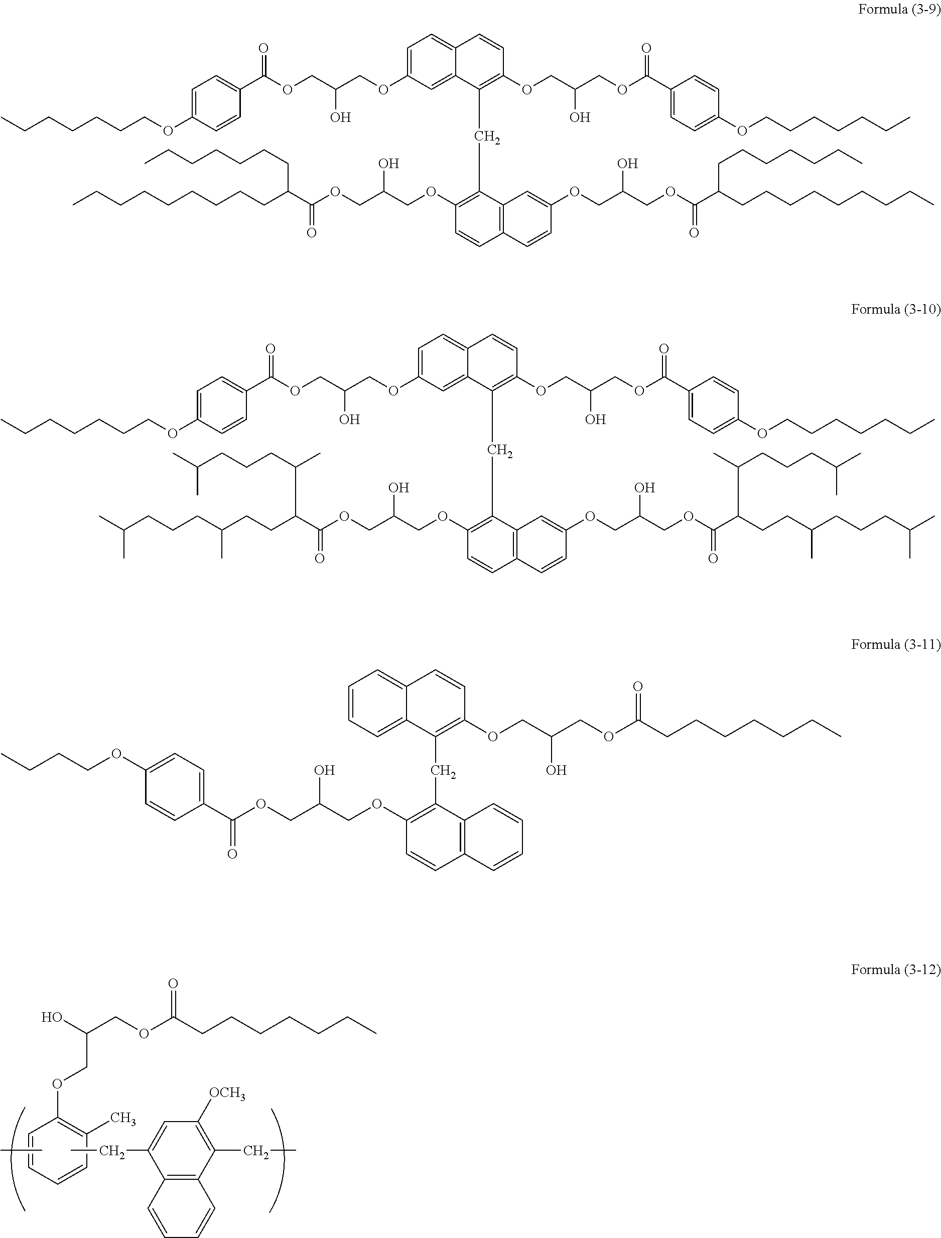
  • the obtained reaction solution contained a polymer of formula (3-9).
  • the weight average molecular weight Mw thereof measured in terms of polystyrene by GPC was 2,600.
  • the obtained reaction solution contained a polymer of formula (3-10).
  • the weight average molecular weight Mw thereof measured in terms of polystyrene by GPC was 2,600.
  • the obtained reaction solution contained a polymer of formula (3-11).
  • the weight average molecular weight Mw thereof measured in terms of polystyrene by GPC was 1,400.
  • the obtained reaction solution contained a polymer of formula (3-12).
  • the weight average molecular weight Mw thereof measured in terms of polystyrene by GPC was 1,500.
  • the obtained reaction solution contained a polymer of formula (3-13).
  • the weight average molecular weight Mw thereof measured in terms of polystyrene by GPC was 1,900.
  • the obtained reaction solution contained a polymer of formula (3-14).
  • the weight average molecular weight Mw thereof measured in terms of polystyrene by GPC was 2,800.
  • the obtained reaction solution contained a polymer of formula (3-15).
  • the weight average molecular weight Mw thereof measured in terms of polystyrene by GPC was 10,000.
  • the obtained reaction solution contained a polymer of formula (3-16).
  • the weight average molecular weight Mw thereof measured in terms of polystyrene by GPC was 1,900.
  • the obtained reaction solution contained a polymer of formula (3-20).
  • the weight average molecular weight Mw thereof measured in terms of polystyrene by GPC was 1,400.
  • the obtained reaction solution contained a polymer of formula (3-21).
  • the weight average molecular weight Mw thereof measured in terms of polystyrene by GPC was 1,800.
  • the obtained reaction solution contained a polymer of the following formula (5-1).
  • the weight average molecular weight Mw thereof measured in terms of polystyrene by GPC was 1,100.
  • the obtained reaction solution contained a polymer of the following formula (5-2).
  • the weight average molecular weight Mw thereof measured in terms of polystyrene by GPC was 1,200.
  • the obtained reaction solution contained a polymer of the following formula (5-3).
  • the weight average molecular weight Mw thereof measured in terms of polystyrene by GPC was 1,300.
  • the resist underlayer film-forming composition prepared in each of Examples 4, 8, 9, 12 to 15, 17, and 21 was applied to a silicon wafer, and heated on a hot plate at 215° C. for 1 minute, to form a film of the resist underlayer film-forming composition.
  • the refractive index at 193 nm and attenuation coefficient of each of the films were measured.
  • an ellipsometer (VUV-VASE) manufactured by J. A. Woollam Japan Corp., was used.
  • the resist underlayer film-forming composition prepared in each of Examples 4, 8, 9, 12 to 15, 17, and 21 was applied to a silicon wafer, and heated on a hot plate at 215° C. for 1 minute, to form a resist underlayer film (stepped substrate-coating film).
  • the dry etching rates of the resist underlayer films were each compared with that of a resist film obtained from a resist solution available from Sumitomo Chemical Co., Ltd., (trade name: SUMIRESIST PAR855).
  • a dry etching device (RIE-10NR) manufactured by Samco Inc. was used. The dry etching rate using CF 4 gas was measured.
  • the refractive index (n value), attenuation coefficient (k value), and ratio of dry etching rate (selection ratio of dry etching rate) of the films of the resist underlayer film-forming compositions are shown in Table 1.
  • the resist underlayer film obtained from the resist underlayer film-forming composition of the present invention had an appropriate anti-reflective effect.
  • a resist film is applied to an upper layer of the resist underlayer film obtained from the resist underlayer film-forming composition of the present invention, exposed, and developed to form a resist pattern, and a substrate is processed by dry etching through the resist pattern using etching gas or the like. At that time, the substrate can be processed since the dry etching rate is higher than that of the resist film.
  • the covering thicknesses at a dense pattern area (DENSE) with a trench width of 50 nm and a pitch of 100 nm and an open area (OPEN) that was unpatterned, of a SiO 2 substrate with a thickness of 200 nm were compared.
  • the resist underlayer film-forming composition of each of Examples 1 to 21 and Comparative Examples 1 to 3 was applied to the substrate so that the thickness was 150 nm, and baked at 215° C. for 60 seconds.
  • the step-covering properties of the substrate were observed by a scanning electron microscope (S-4800) manufactured by Hitachi High-Technologies Corporation, and the difference (difference in level of coating between the dense area and the open area, referred to as Bias) between the film thickness at the dense area (pattern part) and the film thickness at the open area (unpatterned part) was measured.
  • Bias difference in level of coating between the dense area and the open area
  • Table 2 The thickness and the difference in level of coating at each area are shown in Table 2. As the value of Bias is smaller, the flattening properties in the evaluation of flattening properties are higher.
  • Example 1 DENSE OPEN DENSE/OPEN Thickness Thickness Difference in level (nm) (nm) of coating (nm)
  • Example 1 58 nm 135 nm 77 nm
  • Example 2 62 nm 133 nm 72 nm
  • Example 3 70 nm 125 nm 56 nm
  • Example 4 65 nm 107 nm 42 nm
  • Example 5 46 nm 116 nm 70 nm
  • Example 6 75 nm 115 nm 40 nm
  • Example 7 51 nm 112 nm 61 nm
  • Example 8 63 nm 110 nm 47 nm
  • Example 9 64 nm 102 nm 38 nm
  • Example 10 64 nm 102 nm 38 nm
  • Example 11 64 nm 113 nm 46 nm
  • Example 12 77 nm 95 nm 17 nm
  • Example 13 59 nm 101

Landscapes

  • Chemical & Material Sciences (AREA)
  • Physics & Mathematics (AREA)
  • Organic Chemistry (AREA)
  • General Physics & Mathematics (AREA)
  • Engineering & Computer Science (AREA)
  • Health & Medical Sciences (AREA)
  • Chemical Kinetics & Catalysis (AREA)
  • Medicinal Chemistry (AREA)
  • Polymers & Plastics (AREA)
  • Architecture (AREA)
  • Structural Engineering (AREA)
  • Materials Engineering (AREA)
  • Life Sciences & Earth Sciences (AREA)
  • Wood Science & Technology (AREA)
  • Spectroscopy & Molecular Physics (AREA)
  • Materials For Photolithography (AREA)
  • Epoxy Resins (AREA)
  • Manufacturing & Machinery (AREA)
  • Computer Hardware Design (AREA)
  • Microelectronics & Electronic Packaging (AREA)
  • Power Engineering (AREA)
  • Condensed Matter Physics & Semiconductors (AREA)
  • Photosensitive Polymer And Photoresist Processing (AREA)
  • Exposure And Positioning Against Photoresist Photosensitive Materials (AREA)
  • Organic Low-Molecular-Weight Compounds And Preparation Thereof (AREA)
  • Exposure Of Semiconductors, Excluding Electron Or Ion Beam Exposure (AREA)

Abstract

A resist underlayer film-forming composition in which a coating film having high flattening properties is formed on a substrate. A resist underlayer film-forming composition including an epoxy adduct (C) obtained by reacting an epoxy group-containing compound (A) with an epoxy adduct-forming compound (B), wherein one or both of the epoxy group-containing compound (A) and the epoxy adduct-forming compound (B) contain an optionally branched alkyl group having a carbon atom number of three or more. The epoxy adduct-forming compound (B) is at least one compound selected from the group consisting of carboxylic acid (B1), carboxylic anhydride (B2), a phenol compound (B3), a hydroxyl group-containing compound (B4), a thiol compound (B5), an amino compound (B6), and an imide compound (B7). The optionally branched alkyl group having a carbon atom number of three or more is contained in the epoxy adduct-forming compound (B). The optionally branched alkyl group has a C3-19 alkyl group.

Description

TECHNICAL FIELD
The present invention relates to a resist underlayer film-forming composition for formation of a flattened film on a stepped substrate, and a method for producing a laminated substrate that is flattened using a resist underlayer film formed from the composition.
BACKGROUND ART
Conventionally, in production of a semiconductor device, microprocessing by lithography using a photoresist composition has been carried out. The microprocessing is a processing method in which a thin film of the photoresist composition is formed on a substrate to be processed such as a silicon wafer, irradiated with active light such as ultraviolet light through a mask pattern that has a pattern of the semiconductor device, and developed to obtain a photoresist pattern, and the substrate to be processed such as a silicon wafer is etched using the photoresist pattern as a protective film. In recent years, an increase in degree of integration of the semiconductor device advances, and the wavelength of used active light is shortened from a KrF excimer laser (248 nm) to an ArF excimer laser (193 nm). This causes severe problems such as diffuse reflection of active light on a substrate and influence of standing wave. Therefore, a method for providing an anti-reflective coating between the photoresist and the substrate to be processed has been widely applied. For further microprocessing, a lithography technique using extreme ultraviolet light (EUV, 13.5 mm) or an electron beam (EB) as the active light has been also developed. In EUV lithography and EB lithography, since diffuse reflection on a substrate and standing wave do not generally occur, a specific anti-reflective coating is not required, and a resist underlayer film is widely investigated as an auxiliary film for improving resolution properties and adhesion of a resist pattern.
On the other hand, the depth of focus decreases with a decrease in wavelength of exposure light. Therefore, it is important that the flattening properties of a film to be formed on a substrate are improved for formation of a desired resist pattern with precision. Specifically, a resist underlayer film capable of forming a stepless and flat coating film on a substrate is required to produce a semiconductor device having a finer design rule.
For example, a resist underlayer film-forming composition containing a crosslinkable compound having a C2-10 alkoxymethyl group or a C1-10 alkyl group is disclosed (see Patent Document 1). By using the composition, favorable embeddability during applying of the composition to a substrate having a hole pattern is exhibited.
A resist underlayer film-forming composition using a polymer containing in a main chain a structure obtained by reacting an epoxy compound having a C1-10 alkylene group with a compound reactive to the epoxy compound is disclosed (see Patent Document 2).
PRIOR ART DOCUMENTS Patent Documents
    • Patent Document 1: International publication WO2014/208542
    • Patent Document 2: International publication WO2005/098542
SUMMARY OF THE INVENTION Problem to be Solved by the Invention
In order to prevent mixing with a resist underlayer film-forming composition during laminating a photoresist composition and a resist underlayer film different from a resist underlayer film formed from the resist underlayer film-forming composition, a crosslinker or the like is added to the resist underlayer film-forming composition, and the resist underlayer film-forming composition is baked at high temperature to thermally cure a coating film. Thus, the photoresist composition and the different resist underlayer film can be laminated without mixing. However, the resist underlayer film-forming composition having thermosetting properties contains a polymer having a thermal crosslinking-forming functional group such as a hydroxyl group, a crosslinker, and an acid catalyst (acid generator). Therefore, when a pattern (e.g., hole and trench structure) formed on a substrate is filled with the resist underlayer film-forming composition, a crosslinking reaction due to baking is promoted, to increase the viscosity, and as a result, filling properties of the pattern are deteriorated. Accordingly, the flattening properties after formation of a film tends to decrease.
An object of the present invention is to improve the filling properties of the pattern during baking by enhancing the thermal reflow properties of the polymer. Specifically, in order to enhance the thermal reflow properties of the polymer, a long-chain alkyl group capable of decreasing the glass transition temperature of the polymer is introduced. Thus, a resist underlayer film-forming composition in which a decrease in viscosity is sufficiently expressed before a crosslinking reaction during baking starts and a coating film having high flattening properties is formed on a substrate is provided.
Means for Solving the Problems
A first aspect of the present invention is a resist underlayer film-forming composition comprising an epoxy adduct (C) obtained by reacting an epoxy group-containing compound (A) with an epoxy adduct-forming compound (B), wherein one or both of the epoxy group-containing compound (A) and the epoxy adduct-forming compound (B) contain an optionally branched alkyl group having a carbon atom number of three or more.
A second aspect of the present invention is the resist underlayer film-forming composition according to the first aspect, wherein the epoxy adduct-forming compound (B) is at least one compound selected from the group consisting of carboxylic acid (B1), carboxylic anhydride (B2), a phenol compound (B3), a hydroxyl group-containing compound (B4), a thiol compound (B5), an amino compound (B6), and an imide compound (B7).
A third aspect of the present invention is the resist underlayer film-forming composition according to the first or second aspect, wherein the optionally branched alkyl group having a carbon atom number of three or more is contained in the epoxy adduct-forming compound (B).
A fourth aspect of the present invention is the resist underlayer film-forming composition according to any one of the first to third aspects, wherein the optionally branched alkyl group having a carbon atom number of three or more is a C3-19 alkyl group.
A fifth aspect of the present invention is the resist underlayer film-forming composition according to any one of the first to fourth aspects, wherein the epoxy group-containing compound (A) is a compound having a structure of formula (1):
Figure US12242194-20250304-C00001

[wherein PA is a unit structure constituting a compound or a polymer that contains an aliphatic or aromatic hydrocarbon optionally containing an oxygen atom or a nitrogen atom, or a combination thereof, Ep is formula 1A or 1B:
Figure US12242194-20250304-C00002

(wherein a dotted line is a bond), n1 is an integer of 1, n2 and n3 are each an integer of 0 or 1, and n4 is an integer of 1 to 100], or a polymer having a partial structure of the compound.
A sixth aspect of the present invention is the resist underlayer film-forming composition according to any one of the second to fourth aspects, wherein the carboxylic acid (B1) is a compound of formula (2):
Figure US12242194-20250304-C00003

(wherein R1 is an optionally branched alkyl group having a carbon atom number of 3 to 19, Ar1 is a C6-40 arylene group optionally having a substituent, n5 and n6 are each an integer of 0 or 1, n7 is an integer of 1, and n8 is an integer of 1 or 2).
A seventh aspect of the present invention is the resist underlayer film-forming composition according to any one of the second to fourth aspects, wherein the carboxylic anhydride (B2) is a compound of formula (3):
Figure US12242194-20250304-C00004

(wherein Aa is an acid anhydride group, R2 is an optionally branched alkyl group having a carbon atom number of 3 to 19, Ar2 is a C6-40 arylene group optionally having a substituent, n9 and n10 are each an integer of 0 or 1, and n11 is an integer of 1).
An eighth aspect of the present invention is the resist underlayer film-forming composition according to any one of the second to fourth aspects, wherein the phenol compound (B3) is a compound of formula (4):
Figure US12242194-20250304-C00005

(wherein R3 is an optionally branched alkyl group having a carbon atom number of 3 to 19, Ar3 is a C6-40 arylene group optionally having a substituent, n12 is an integer of 0 or 1, n13 is an integer of 1, n14 is an integer of 1, and n15 is an integer of 1 to 3).
A ninth aspect of the present invention is the resist underlayer film-forming composition according to any one of the second to fourth aspects, wherein the hydroxyl group-containing compound (B4) is a compound of formula (5):
Figure US12242194-20250304-C00006

(wherein R4 is an optionally branched alkyl group having a carbon atom number of 3 to 19, n16 is an integer of 1 to 3, and n17 is an integer of 1).
A tenth aspect of the present invention is the resist underlayer film-forming composition according to any one of the second to fourth aspects, wherein the thiol compound (B5) is a compound of formula (6):
Figure US12242194-20250304-C00007

(wherein R5 is an optionally branched alkyl group having a carbon atom number of 3 to 19, Ar4 is a C6-40 arylene group optionally having a substituent, n18 and n19 are each an integer of 0 or 1, n20 is an integer of 1, and n21 is an integer of 1 to 3).
An eleventh aspect of the present invention is the resist underlayer film-forming composition according to any one of the second to fourth aspects, wherein the amino compound (B6) is a compound of formula (7):
Figure US12242194-20250304-C00008

(wherein Ab is a primary amino group, a secondary amino group, or a tertiary amino group, R6 is an optionally branched alkyl group having a carbon atom number of 3 to 19, Ar5 is a C6-40 arylene group optionally having a substituent, n22 and n23 are each an integer of 0 or 1, n24 is an integer of 1, and n25 is an integer of 1 to 3).
A twelfth aspect of the present invention is the resist underlayer film-forming composition according to any one of the second to fourth aspects, wherein the imide compound (B7) is a compound of formula (8):
Figure US12242194-20250304-C00009

(wherein Ac is an imido group having active hydrogen, R7 is an optionally branched alkyl group having a carbon atom number of 3 to 19, Ar6 is a C6-40 arylene group optionally having a substituent, n26 and n27 are each an integer of 0 or 1, n28 is an integer of 1, and n29 is an integer of 1).
A thirteenth aspect of the present invention is the resist underlayer film-forming composition according to any one of the first to twelfth aspects, wherein the epoxy adduct (C) is formed by reacting an epoxy group-containing compound (A) having at least two epoxy groups with an epoxy adduct-forming compound (B) having an epoxy addition reactive group.
A fourteenth aspect of the present invention is the resist underlayer film-forming composition according to any one of the first to thirteenth aspects, further comprising a crosslinker.
A fifteenth aspect of the present invention is the resist underlayer film-forming composition according to any one of the first to fourteenth aspects, further comprising an acid or an acid generator.
A sixteenth aspect of the present invention is a resist underlayer film formed on a semiconductor substrate from a cured product of the resist underlayer film-forming composition according to any one of the first to fifteenth aspects.
A seventeenth aspect of the present invention is a method for producing a semiconductor device comprising steps of forming an underlayer film on a semiconductor substrate from the resist underlayer film-forming composition according to any one of the first to fifteenth aspects, forming a resist film on the underlayer film, forming a resist pattern by irradiation with light or an electron beam and development, etching the underlayer film through the formed resist pattern, and processing the semiconductor substrate through the patterned underlayer film.
An eighteenth aspect of the present invention is a method for producing a semiconductor device comprising steps of forming an underlayer film on a semiconductor substrate from the resist underlayer film-forming composition according to any one of the first to fifteenth aspects, forming a hard mask on the underlayer film, forming a resist film on the hard mask, forming a resist pattern by irradiation with light or an electron beam and development, etching the hard mask through the formed resist pattern, etching the underlayer film through the patterned hard mask, and processing the semiconductor substrate through the patterned underlayer film.
Effects of the Invention
In the resist underlayer film-forming composition of the present invention, the thermal reflow properties during baking are enhanced by imparting a long-chain alkyl group capable of decreasing the glass transition temperature (Tg) of a polymer to a skeleton of a main resin in the resist underlayer film-forming composition.
Therefore, when the resist underlayer film-forming composition of the present invention is applied to a substrate and baked, the filling properties of a pattern on the substrate can be improved due to high thermal reflow properties of the polymer.
By the resist underlayer film-forming composition of the present invention, a flat film can be formed on the substrate regardless of an open area (unpatterned area) and a pattern area of DENSE (dense) and ISO (coarse) on the substrate.
Therefore, the resist underlayer film-forming composition of the present invention satisfies both the filling properties of the pattern and the flattening properties after filling, and an excellent flattened film can be formed.
Further, the resist underlayer film-forming composition of the present invention has an appropriate anti-reflective effect and a dry etching rate higher than that of a resist film. Therefore, the substrate can be processed.
MODES FOR CARRYING OUT THE INVENTION
The present invention is a resist underlayer film-forming composition comprising an epoxy adduct (C) obtained by reacting an epoxy group-containing compound (A) with an epoxy adduct-forming compound (B), wherein one or both of the epoxy group-containing compound (A) and the epoxy adduct-forming compound (B) contain an optionally branched alkyl group having a carbon atom number of three or more.
In the present invention, the resist underlayer film-forming composition for lithography contains the above-described resin and a solvent. The composition can contain a crosslinker, an acid, an acid generator, a surfactant, or the like, if necessary. The solid content of the composition is 0.1 to 70% by mass, or 0.1 to 60% by mass.
The solid content is a content ratio of all components other than the solvent in the resist underlayer film-forming composition. The epoxy adduct (C) can be contained in an amount of 1 to 100% by mass, 1 to 99.9% by mass, 50 to 99.9% by mass, 50 to 95% by mass, or 50 to 90% by mass, in the solid content.
As the optionally branched alkyl group having a carbon atom number of three or more in the present invention, for example, an optionally branched alkyl group having a carbon atom number of 3 to 19 can be used. Further, hydrogen atoms may be partially substituted with a hydroxyl group, a nitro group, a cyano group, or a halogen atom (fluorine, chlorine, bromine, iodine).
The alkyl group may be a C3-19 alkyl group, and examples thereof include n-propyl group, i-propyl group, cyclopropyl group, n-butyl group, i-butyl group, s-butyl group, t-butyl group, cyclobutyl group, 1-methyl-cyclopropyl group, 2-methyl-cyclopropyl group, n-pentyl group, 1-methyl-n-butyl group, 2-methyl-n-butyl group, 3-methyl-n-butyl group, 1,1-dimethyl-n-propyl group, 1,2-dimethyl-n-propyl group, 2,2-dimethyl-n-propyl group, 1-ethyl-n-propyl group, cyclopentyl group, 1-methyl-cyclobutyl group, 2-methyl-cyclobutyl group, 3-methyl-cyclobutyl group, 1,2-dimethyl-cyclopropyl group, 2,3-dimethyl-cyclopropyl group, 1-ethyl-cyclopropyl group, 2-ethyl-cyclopropyl group, n-hexyl group, 1-methyl-n-pentyl group, 2-methyl-n-pentyl group, 3-methyl-n-pentyl group, 4-methyl-n-pentyl group, 1,1-dimethyl-n-butyl group, 1,2-dimethyl-n-butyl group, 1,3-dimethyl-n-butyl group, 2,2-dimethyl-n-butyl group, 2,3-dimethyl-n-butyl group, 3,3-dimethyl-n-butyl group, 1-ethyl-n-butyl group, 2-ethyl-n-butyl group, 1,1,2-trimethyl-n-propyl group, 1,2,2-trimethyl-n-propyl group, 1-ethyl-1-methyl-n-propyl group, 1-ethyl-2-methyl-n-propyl group, n-heptyl group, 2-ethyl-hexyl group, n-octyl group, n-nonyl group, n-decyl group, n-undecyl group, n-dodecyl group, n-tridecyl group, n-tetradecyl group, n-pentadecyl group, n-hexadecyl group, n-heptadecyl group, 2-heptyl-undecyl group, n-octadecyl group, n-nonadecyl group, 5,9-dimethyl-2-(6-methylhepthyl)decyl group, cyclohexyl group, 1-methyl-cyclopentyl group, 2-methyl-cyclopentyl group, 3-methyl-cyclopentyl group, 1-ethyl-cyclobutyl group, 2-ethyl-cyclobutyl group, 3-ethyl-cyclobutyl group, 1,2-dimethyl-cyclobutyl group, 1,3-dimethyl-cyclobutyl group, 2,2-dimethyl-cyclobutyl group, 2,3-dimethyl-cyclobutyl group, 2,4-dimethyl-cyclobutyl group, 3,3-dimethyl-cyclobutyl group, 1-n-propyl-cyclopropyl group, 2-n-propyl-cyclopropyl group, 1-i-propyl-cyclopropyl group, 2-i-propyl-cyclopropyl group, 1,2,2-trimethyl-cyclopropyl group, 1,2,3-trimethyl-cyclopropyl group, 2,2,3-trimethyl-cyclopropyl group, I-ethyl-2-methyl-cyclopropyl group, 2-ethyl-1-methyl-cyclopropyl group, 2-ethyl-2-methyl-cyclopropyl group, and 2-ethyl-3-methyl-cyclopropyl group.
As the epoxy group-containing compound (A) used in the present invention, a compound having a structure of formula (1) or a polymer having a partial structure thereof can be used.
When the epoxy group-containing compound (A) is the polymer, the weight average molecular weight thereof can fall within a range of 500 to 100,000.
In formula (1), PA is a unit structure constituting a compound or a polymer that contains an aliphatic or aromatic hydrocarbon optionally containing an oxygen atom or a nitrogen atom, or a combination thereof. When PA contains an oxygen atom, PA may have a hydroxyl group as a substituent, or an ether structure, a ketone structure, or an ester structure in a main chain structure.
Ep is a group of formula (1A) or (1B). In formulae (1A) and (1B), a dotted line is a bond. n1 is an integer of 1, n2 and n3 are each an integer of 0 or 1, and n4 is an integer of 1 to 100. When the epoxy group-containing compound (A) is the compound, n4 is 1 to 10, 1 to 4, or 2 to 4. When the epoxy group-containing compound (A) is the polymer, n4 can fall within a range of 1 to 100 or 2 to 100, and n4 can be at least 2.
Examples of the epoxy group-containing compound (A) include an epoxy group-containing benzene or epoxy group-containing benzene fused cyclic compound, an epoxy group-containing aliphatic polyether, an epoxy group-containing novolak polymer, a polyether of epoxy group-containing alicyclic hydrocarbon, and an epoxy group-containing polyester. Examples thereof include as follows.
Figure US12242194-20250304-C00010
Figure US12242194-20250304-C00011
Figure US12242194-20250304-C00012
Figure US12242194-20250304-C00013
The compounds described above are available as commercial products.
The compound of formula (1-1) is trade name EPOLEAD GT401 available from Daicel Corporation. In formula (1-1), a, b, c, and d are each 0 or 1, and a+b+c+d is 1.
The compound of formula (1-2) can be obtained as trade name YH-434L available from NIPPON STEEL & SUMIKIN CHEMICAL CO., LTD.
The compound of formula (1-3) can be obtained as trade name EX-411 available from Nagase ChemteX Corporation.
The compound of formula (1-4) can be obtained as trade name EX-521 available from Nagase ChemteX Corporation.
The compound of formula (1-5) can be obtained as trade name EX-611 available from Nagase ChemteX Corporation.
The compound of formula (1-6) can be obtained as trade name EPICLON HP-4770 available from DIC Corporation.
The compound of formula (1-7) can be obtained as trade name EPICLON HP-4700 available from DIC Corporation.
The compound of formula (1-8) can be obtained as trade name TEP-G available from Asahi Organic Chemicals Industry Co., Ltd.
The compound of formula (1-9) can be obtained as trade name EHPE-3150 available from Daicel Corporation.
The compound of formula (1-10) can be obtained as trade name EPPN-201 available from NIPPON KAYAKU Co., Ltd.
The compound of formula (1-11) can be obtained as trade name ECN-1229 available from Asahi Kasei Epoxy Co., Ltd.
The compound of formula (1-12) can be obtained as trade name EPPN-501H available from NIPPON KAYAKU Co., Ltd.
The compound of formula (1-13) can be obtained as trade name NC-2000L available from NIPPON KAYAKU Co., Ltd.
The compound of formula (1-14) can be obtained as trade name NC-3000L available from NIPPON KAYAKU Co., Ltd.
The compound of formula (1-15) can be obtained as trade name NC-7000L available from NIPPON KAYAKU Co., Ltd.
The compound of formula (1-16) can be obtained as trade name NC-7300L available from NIPPON KAYAKU Co., Ltd.
The compound of formula (1-17) can be obtained as trade name EPICLON HP-5000 available from DIC Corporation.
For example, other epoxy resins can be obtained as trade name EPICLON HP-6000 and the like available from DIC Corporation.
As the epoxy adduct-forming compound (B) used in the present invention, at least one compound selected from the group consisting of carboxylic acid (B1), carboxylic anhydride (B2), a phenol compound (B3), a hydroxyl group-containing compound (B4), a thiol compound (B5), an amino compound (B6), and an imide compound (B7) can be used.
As the epoxy adduct-forming compound (B), the carboxylic acid (B1), the phenol compound (B3), or a mixture thereof can be used.
The epoxy adduct-forming compound (B) can contain an optionally branched alkyl group having a carbon atom number of three or more, preferably a carbon atom number of 3 to 19.
As the carboxylic acid (B1), a compound of formula (2) can be used. In formula (2), R1 is an optionally branched alkyl group having a carbon atom number of 3 to 19, Ar1 is a C6-40 arylene group optionally having a substituent, n5 and n6 are each an integer of 0 or 1, n7 is an integer of 1, and n8 is an integer of 1 or 2. As n8, an integer of 1 can be selected, and in this case, the number of carboxylic acid group in the molecule is one.
Examples of the C6-40 arylene group include arylene groups derived from the following aryl groups or substituted aryl groups. Further, hydrogen atoms may be partially substituted with a hydroxyl group, a nitro group, a cyano group, or a halogen atom (fluorine, chlorine, bromine, iodine).
Examples of the aryl groups or substituted aryl groups include phenyl group, o-methylphenyl group, m-methylphenyl group, p-methylphenyl group, o-chlorophenyl group, m-chlorophenyl group, p-chlorophenyl group, o-fluorophenyl group, p-fluorophenyl group, o-methoxyphenyl group, p-methoxyphenyl group, p-nitrophenyl group, p-cyanophenyl group, α-naphthyl group, β-naphthyl group, o-biphenylyl group, m-biphenylyl group, p-biphenylyl group, 1-anthryl group, 2-anthryl group, 9-anthryl group, 1-phenanthryl group, 2-phenanthryl group, 3-phenanthryl group, 4-phenanthryl group, and 9-phenanthryl group.
As the carboxylic anhydride (B2), a compound of formula (3) can be used. In formula (3), Aa is an acid anhydride group, R2 is an optionally branched alkyl group having a carbon atom number of 3 to 19, Ar2 is a C6-40 arylene group optionally having a substituent, n9 and n10 are each an integer of 0 or 1, and n11 is an integer of 1. Examples of the arylene group can be those exemplified as described above. The carboxylic anhydride (B2) is a compound having one carboxylic anhydride group in the molecule.
As the phenol compound (B3), a compound of formula (4) can be used. In formula (4), R3 is an optionally branched alkyl group having a carbon atom number of 3 to 19, Ar3 is a C6-40 arylene group optionally having a substituent, n12 is an integer of 0 or 1, n13 is an integer of 1, n14 is an integer of 1, and n15 is an integer of 1 to 3. n15 may be an integer of 1. Examples of the arylene group can be those exemplified as described above. As n15, an integer of 1 may be selected, and in this case, the number of hydroxyl group in the molecule is one.
As the hydroxyl group-containing compound (B4), a compound of formula (5) can be used. In formula (5), R4 is an optionally branched alkyl group having a carbon atom number of 3 to 19, n16 is an integer of 1 to 3, and n17 is an integer of 1. As n16, an integer of 1 can be selected, and in this case, the number of hydroxyl group in the molecule is one.
As the thiol compound (B5), a compound of formula (6) can be used. In formula (6), R5 is an optionally branched alkyl group having a carbon atom number of 3 to 19, Ar4 is a C6-40 arylene group optionally having a substituent, n18 and n19 are each an integer of 0 or 1, n20 is an integer of 1, and n21 is an integer of 1 to 3. Examples of the arylene group can be those exemplified as described above. As n21, an integer of 1 can be selected, and in this case, the number of thiol group in the molecule is one.
As the amino compound (B6), a compound of formula (7) can be used. In formula (7), Ab is a primary amino group, a secondary amino group, or a tertiary amino group, R6 is an optionally branched alkyl group having a carbon atom number of 3 to 19, Ar5 is a C6-40 arylene group optionally having a substituent, n22 and n23 are each an integer of 0 or 1, n24 is an integer of 1, and n25 is an integer of 1 to 3. Examples of the arylene group can be those exemplified as described above. As n25, an integer of 1 can be selected, and in this case, the number of amino group in the molecule is one. When Ab is a tertiary amino group, the tertiary amino group acts to promote addition of alcohol to an epoxy group.
As the imide compound (B7), a compound of formula (8) can be used. In formula (8), Ac is an imido group having active hydrogen, R7 is an optionally branched alkyl group having a carbon atom number of 3 to 19, Ar6 is a C6-40 arylene group optionally having a substituent, n26 and n27 are each an integer of 0 or 1, n28 is an integer of 1, and n29 is an integer of 1. Examples of the arylene group can be those exemplified as described above. As n29, an integer of 1 can be selected, and in this case, the number of imido group in the molecule is one.
Examples of the epoxy adduct-forming compound (B) include as follows.
Figure US12242194-20250304-C00014
Figure US12242194-20250304-C00015
Figure US12242194-20250304-C00016
In the present invention, as the epoxy adduct (C), an epoxy adduct (C) formed by reacting the epoxy group-containing compound (A) having at least two epoxy groups with the epoxy adduct-forming compound (B) having an epoxy addition reactive group can be used.
Examples of the epoxy adduct (C) include as follows.
Figure US12242194-20250304-C00017
Figure US12242194-20250304-C00018
Figure US12242194-20250304-C00019
Figure US12242194-20250304-C00020

(wherein a, b, c, and d are each 0 or 1, and a+b+c+d is 1).
Figure US12242194-20250304-C00021
Figure US12242194-20250304-C00022
The resist underlayer film-forming composition of the present invention can contain a crosslinker component. Examples of the crosslinker include compounds such as a melamine-based crosslinker, a substituted urea-based crosslinker, and polymers thereof. A crosslinker having at least two crosslinking-forming substituents is preferable. Examples thereof include compounds such as methoxymethylated glycoluril, butoxymethylated glycoluril, methoxymethylated melamine, butoxymethylated melamine, methoxymethylated benzoguanamine, butoxymethylated benzoguanamine, methoxymethylated urea, butoxymethylated urea, methoxymethylated thiourea, and methoxymethylated thiourea. A condensate of the compounds can be also used.
As the crosslinker, a crosslinker having high heat resistance can be used. As the crosslinker having high heat resistance, a compound having a crosslinking-forming substituent having an aromatic ring (e.g., benzene ring and naphthalene ring) in the molecule can be used.
Examples of the compound include a compound having a partial structure of the following formula (3A), and a polymer and an oligomer having a repeating unit of the following formula (3B).
Figure US12242194-20250304-C00023

R11, R12, R13, and R14 described above are a hydrogen atom or a C1-10 alkyl group, and as the alkyl group, the aforementioned examples can be used.
m1 is an integer satisfying 1≤m1≤6−m2. m2 is an integer satisfying 1≤m2≤5. m3 is an integer satisfying 1≤m3≤4−m2. m4 is an integer satisfying 1≤m4≤3.
Examples of the compound of formula (3A) and the polymer and oligomer of formula (3B) include as follows.
Figure US12242194-20250304-C00024
Figure US12242194-20250304-C00025
Figure US12242194-20250304-C00026
Figure US12242194-20250304-C00027
Figure US12242194-20250304-C00028
The compounds are available as products available from Asahi Organic Chemicals Industry Co., Ltd., and Honshu Chemical Industry Co., Ltd. Among the crosslinkers, for example, the compound of formula (4-24) is available as trade name TM-BIP-A available from Asahi Organic Chemicals Industry Co., Ltd.
The amount of crosslinker to be added varies depending on a coating solvent to be used, an underlying substrate to be used, a solution viscosity to be required, and a film form to be required. The amount is 0.001 to 80% by mass, preferably 0.01 to 50% by mass, and further preferably 0.05 to 40% by mass, relative to the total solid content. The crosslinker may cause a crosslinking reaction due to self-condensation. However, when the polymer in the present invention has a crosslinkable substituent, the crosslinker may cause a crosslinking reaction with the crosslinkable substituent.
In the present invention, as a catalyst for promoting the crosslinking reaction, an acid and/or an acid generator can be added. For example, an acidic compound such as p-toluenesulfonic acid, trifluoromethanesulfonic acid, pyridinium p-toluenesulfonic acid, salicylic acid, 5-sulfosalicylic acid, 4-phenolsulfonic acid, camphorsulfonic acid, 4-chlorobenzenesulfonic acid, benzenedisulfonic acid, 1-naphthalenesulfonic acid, citric acid, benzoic acid, hydroxybenzoic acid, or naphthalenecarboxylic acid, and/or a thermal acid generator such as 2,4,4,6-tetrabromocyclohexadienone, benzoin tosylate, 2-nitrobenzyl tosylate, or another organic alkyl sulfonate can be mixed. The amount of the catalyst to be mixed is 0.0001 to 20% by mass, preferably 0.0005 to 10% by mass, and more preferably 0.01 to 3% by mass, relative to the total solid content.
The resist underlayer film-forming composition for lithography of the present invention can contain a photoacid generator in order to coincide the acidity of a photoresist covering an upper layer in a lithography process. Preferable examples of the photoacid generator include onium salt-based photoacid generators such as bis(4-t-butylphenyl)iodonium trifluoromethanesulfonate and triphenylsulfonium trifluoromethanesulfonate, halogen-containing compound-based photoacid generators such as phenyl-bis(trichloromethyl)-s-triazine, and sulfonic acid-based photoacid generators such as benzoin tosylate and N-hydroxysuccinimide trifluoromethanesulfonate. The amount of the photoacid generator is 0.2 to 10% by mass, and preferably 0.4 to 5% by mass, relative to the total solid content.
In addition to the above, the resist underlayer film-forming composition for lithography of the present invention can further contain a light absorber, a rheology controlling agent, an adhesive adjuvant, a surfactant, or the like, if necessary.
As the light absorber, a commercially available light absorber described in “Kogyoyoshikiso no gijutsu to shijo” (CMC Publishing Co., Ltd.) or “Senryo binran” (edited by The Society of Synthetic Organic Chemistry, Japan.), C.I.Disperse Yellow 1, 3, 4, 5, 7, 8, 13, 23, 31, 49, 50, 51, 54, 60, 64, 66, 68, 79, 82, 88, 90, 93, 102, 114 or 124; C.I.Disperse Orange 1, 5, 13, 25, 29, 30, 31, 44, 57, 72 or 73; C.I.Disperse Red 1, 5, 7, 13, 17, 19, 43, 50, 54, 58, 65, 72, 73, 88, 117, 137, 143, 199, or 210; C.I.Disperse Violet 43; C.I.Disperse Blue 96; C.I.Fluorescent Brightening Agent 112, 135, or 163; C.I.Solvent Orange 2 or 45; C.I.Solvent Red 1, 3, 8, 23, 24, 25, 27, or 49; C.I.Pigment Green 10; C.I.Pigment Brown 2 or the like can be suitably used. The light absorber is usually mixed in an amount of 10% by mass or less, and preferably 5% by mass or less, relative to the total solid content of the resist underlayer film-forming composition for lithography.
The rheology controlling agent is added to mainly improve the flowability of the resist underlayer film-forming composition, and in particular, to improve the film thickness uniformity of the resist underlayer film and enhance the filling properties of the inside of holes with the resist underlayer film-forming composition in a baking step. Specific examples thereof include phthalic acid derivatives such as dimethyl phthalate, diethyl phthalate, diisobutyl phthalate, dihexyl phthalate, and butylisodecyl phthalate, adipic acid derivatives such as di-n-butyl adipate, diisobutyl adipate, diisooctyl adipate, and octyldecyl adipate, maleic acid derivatives such as di-n-butyl maleate, diethyl maleate, and dinonyl maleate, oleic acid derivatives such as methyl oleate, butyl oleate, and tetrahydrofurfuryl oleate, and stearic acid derivatives such as n-butyl stearate and glyceryl stearate. The rheology controlling agent is usually mixed in an amount of less than 30% by mass, relative to the total solid content of the resist underlayer film-forming composition for lithography.
The adhesive adjuvant is added to mainly improve the adhesion of a substrate or a resist to the resist underlayer film-forming composition, and in particular, to prevent peeling of the resist by development. Specific examples thereof include chlorosilanes such as trimethylchlorosilane, dimethylvinylchlorosilane, methyldiphenylchlorosilane, and chloromethyldimethylchlorosilane, alkoxysilanes such as trimethylmethoxysilane, dimethyldiethoxysilane, methyldimethoxysilane, dimethylvinylethoxysilane, diphenyldimethoxysilane, and phenyltriethoxysilane, silazanes such as hexamethyldisilazane, N,N′-bis(trimethylsilyl)urea, dimethyltrimethylsilylamine, and trimethylsilyl imidazole, silanes such as vinyltrichlorosilane, γ-chloropropyltrimethoxysilane, γ-aminopropyltriethoxysilane, and γ-glycidoxypropyltrimethoxysilane, heterocyclic compounds such as benzotriazole, benzimidazole, indazole, imidazole, 2-mercaptobenzimidazole, 2-mercaptobenzothiazole, 2-mercaptobenzoxazole, urazole, thiouracil, mercaptoimidazole, and mercaptopyrimidine, urea compounds such as 1,1-dimethylurea and 1,3-dimethylurea, and thiourea compounds. The adhesive adjuvant is usually mixed in an amount of less than 5% by mass, and preferably less than 2% by mass, relative to the total solid content of the resist underlayer film-forming composition for lithography.
In the resist underlayer film-forming composition for lithography of the present invention, a surfactant can be mixed to further improve the applying properties against unevenness of a surface without generation of pinholes, striation, and the like. Examples of the surfactant include nonionic surfactants including polyoxyethylene alkyl ethers such as polyoxyethylene lauryl ether, polyoxyethylene stearyl ether, polyoxyethylene cetyl ether, and polyoxyethylene oleyl ether, polyoxyethylene alkylaryl ethers such as polyoxyethylene octylphenol ether and polyoxyethylene nonylphenol ether, polyoxyethylene-polyoxypropylene block copolymers, sorbitan fatty acid esters such as sorbitan monolaurate, sorbitan monopalmitate, sorbitan monostearate, sorbitan monooleate, sorbitan trioleate, and sorbitan tristearate, and polyoxyethylene sorbitan fatty acid esters such as polyoxyethylene sorbitan monolaurate, polyoxyethylene sorbitan monopalmitate, polyoxyethylene sorbitan monostearate, polyoxyethylene sorbitan trioleate, and polyoxyethylene sorbitan tristearate, fluorosurfactants including Eftop EF301, EF303, and EF352 (trade name, available from Tohkem Products Corporation), MEGAFACE F171, F173, R-40, and R-40N (trade name, available from DIC Corporation), Fluorad FC430 and FC431 (trade name, available from Sumitomo 3M, Ltd.), Asahi Guard AG710, and Surflon S-382, SC101, SC102, SC103, SC104, SC105, and SC106 (trade name, available from Asahi Glass Co., Ltd.), and organosiloxane polymer KP341 (available from Shin-Etsu Chemical Co., Ltd.). The amount of surfactant to be mixed is usually 2.0% by mass or less, and preferably 1.0% by mass or less, relative to the total solid content of the resist underlayer film-forming composition for lithography of the present invention. The surfactant may be added alone or two or more kinds thereof may be added in combination.
In the present invention, as a solvent capable of dissolving the polymer, the crosslinker component, the crosslinking catalyst, and the like, ethylene glycol monomethyl ether, ethylene glycol monoethyl ether, methyl cellosolve acetate, ethyl cellosolve acetate, diethylene glycol monomethyl ether, diethylene glycol monoethyl ether, propylene glycol, propylene glycol monomethyl ether, propylene glycol monomethyl ether acetate, propylene glycol monoethyl ether, propylene glycol monoethyl ether acetate, propylene glycol propyl ether acetate, toluene, xylene, methyl ethyl ketone, cyclopentanone, cyclohexanone, ethyl 2-hydroxypropionate, ethyl 2-hydroxy-2-methylpropionate, ethyl ethoxyacetate, ethyl hydroxyacetate, methyl 2-hydroxy-3-methylbutanoate, methyl 3-methoxypropionate, ethyl 3-methoxypropionate, ethyl 3-ethoxypropionate, methyl 3-ethoxypropionate, methyl pyruvate, ethyl pyruvate, ethyl acetate, butyl acetate, ethyl lactate, butyl lactate, or the like can be used. The organic solvent may be used alone, or two or more types thereof may be used in combination.
Further, a solvent having a high boiling point such as propylene glycol monobutyl ether or propylene glycol monobutyl ether acetate can be mixed and used. Among the solvents, propylene glycol monomethyl ether, propylene glycol monomethyl ether acetate, ethyl lactate, butyl lactate, and cyclohexanone are preferable in terms of improved leveling properties. In particular, propylene glycol monomethyl ether and propylene glycol monomethyl ether acetate are preferable.
The resin used in the present invention exhibits high solubility in the solvent generally used in the lithography process, such as propylene glycol monomethyl ether and propylene glycol monomethyl ether acetate.
A resist used in the present invention is a photoresist or an electron beam resist.
As a photoresist applied to the top of the resist underlayer film for lithography in the present invention, any of a negative photoresist and a positive photoresist can be used. Examples thereof include a positive photoresist including a novolac resin and 1,2-naphthoquinone diazide sulfonic acid ester; a chemically amplified photoresist including a binder having a group that increases an alkali dissolution rate by decomposition with an acid, and a photoacid generator; a chemically amplified photoresist including an alkaline soluble binder, a low molecular compound that increases the alkali dissolution rate of the photoresist by decomposition with an acid, and a photoacid generator; a chemically amplified photoresist including a binder having a group that increases the alkali dissolution rate by decomposition with an acid, a low molecular compound that increases the alkali dissolution rate of the photoresist by decomposition with the acid, and a photoacid generator; and a photoresist having a Si atom in the skeleton. Specific examples thereof include trade name APEX-E available from Rohm and Haas.
Examples of an electron beam resist applied to the top of the resist underlayer film for lithography in the present invention include a composition including a resin having a Si—Si bond in the main chain and an aromatic ring at the terminal and an acid generator that generates an acid by irradiation with an electron beam; or a composition including poly(p-hydroxyl styrene) of which a hydroxyl group is substituted with an organic group containing N-carboxyamine and an acid generator that generates an acid by irradiation with an electron beam. In the latter electron beam resist composition, an acid generated from the acid generator by irradiation with an electron beam is reacted with a N-carboxyaminoxy group of a polymer side chain to decompose the polymer side chain into a hydroxyl group. Thus, the electron beam resist composition exhibits alkaline solubility, and is dissolved in an alkaline developer to form a resist pattern. Examples of the acid generator that generates an acid by irradiation with an electron beam include halogenated organic compounds such as 1,1-bis[p-chlorophenyl]-2,2,2-trichloroethane, 1,1-bis[p-methoxyphenyl]-2,2,2-trichloroethane, 1,1-bis[p-chlorophenyl]-2,2-dichloroethane, and 2-chloro-6-(trichloromethyl)pyridine, onium salts such as a triphenyl sulfonium salt and a diphenyliodonium salt, and sulfonate esters such as nitrobenzyl tosylate and dinitrobenzyl tosylate.
As a developer of the resist having the resist underlayer film formed from the resist underlayer film-forming composition for lithography of the present invention, an aqueous solution of an alkali including an inorganic alkali such as sodium hydroxide, potassium hydroxide, sodium carbonate, sodium silicate, sodium methasilicate, or ammonia water, a primary amine such as ethylamine or n-propylamine, a secondary amine such as diethylamine or di-n-butylamine, a tertiary amine such as triethylamine or methyldiethylamine, an alcoholamine such as dimethylethanolamine or triethanolamine, a quaternary ammonium salt such as tetramethylammonium hydroxide, tetraethylammonium hydroxide, or choline, or a cyclic amine such as pyrrole or piperidine can be used. A solution in which proper amounts of an alcohol such as isopropyl alcohol and a surfactant such as a nonionic surfactant are added to the aqueous solution of the alkali can be also used. Among the developers, a quaternary ammonium salt is preferable, and tetramethylammonium hydroxide and choline are further preferable.
As the developer, an organic solvent may be used. Examples thereof include methyl acetate, butyl acetate, ethyl acetate, isopropyl acetate, amyl acetate, isoamyl acetate, ethyl methoxyacetate, ethyl ethoxyacetate, 2-heptanone, propylene glycol monomethyl ether acetate, ethylene glycol monoethyl ether acetate, ethylene glycol monopropyl ether acetate, ethylene glycol monobutyl ether acetate, ethylene glycol monophenyl ether acetate, diethylene glycol monomethyl ether acetate, diethylene glycol monopropyl ether acetate, diethylene glycol monoethyl ether acetate, diethylene glycol monopropyl ether acetate, diethylene glycol monoethyl ether acetate, 2-methoxybutyl acetate, 3-methoxybutyl acetate, 4-methoxybutyl acetate, 3-methyl-3-methoxybutyl acetate, 3-ethyl-3-methoxybutyl acetate, propylene glycol monoethyl ether acetate, propylene glycol monopropyl ether acetate, 2-ethoxybutyl acetate, 4-ethoxybutyl acetate, 4-propoxybutyl acetate, 2-methoxypentyl acetate, 3-methoxypentyl acetate, 4-methoxypentyl acetate, 2-methyl-3-methoxypentyl acetate, 3-methyl-3-methoxypentyl acetate, 3-methyl-4-methoxypentyl acetate, 4-methyl-4-methoxypentyl acetate, propylene glycol diacetate, methyl formate, ethyl formate, butyl formate, propyl formate, ethyl lactate, butyl lactate, propyl lactate, ethyl carbonate, propyl carbonate, butyl carbonate, methyl pyruvate, ethyl pyruvate, propyl pyruvate, butyl pyruvate, methyl acetoacetate, ethyl acetoacetate, methyl propionate, ethyl propionate, propyl propionate, isopropyl propionate, methyl 2-hydroxypropionate, ethyl 2-hydroxypropionate, methyl 3-methoxypropionate, ethyl 3-methoxypropionate, ethyl 3-ethoxypropionate, and propyl 3-methoxypropionate. As the developer, butyl acetate, 2-heptanone, or the like can be preferably used.
Further, a surfactant or the like can be added to the developer. A development condition is appropriately selected from a temperature of 5 to 50° C. and a time of 10 to 600 seconds.
Next, a method for forming a resist pattern in the present invention will be described. The resist underlayer film-forming composition is applied to a substrate used in production of a precision integrated circuit element (e.g., a transparent substrate such as a silicon/silicon dioxide coating, a glass substrate, and an ITO substrate) by an appropriate coating means such as a spinner or a coater, baked, and cured to form a coating underlayer film. Herein, the thickness of the resist underlayer film is preferably 0.01 to 3.0 μm. A baking (curing) condition after applying is at 80 to 400° C. for 0.5 to 120 minutes. After then, the resist is applied directly to the resist underlayer film, or if necessary, the resist is applied after one or more layers of coating material are formed on the coating underlayer film. The resist is irradiated with light or an electron beam through a predetermined mask, developed, washed, and dried. Thus, a good resist pattern can be obtained. If necessary, post exposure bake (PEB) with light or an electron beam can be also carried out. The resist underlayer film at a portion where the resist is developed and removed in the step described above can be removed by dry etching, to form a desired pattern on the substrate.
The exposure light for the photoresist is actinic radiation such as near ultraviolet light, far ultraviolet light, or extreme ultraviolet light (e.g., EUV, wavelength: 13.5 nm). For example, light having a wavelength of 248 nm (KrF laser beam), 193 nm (ArF laser beam), or 157 nm (F2 laser beam) can be used. A method for irradiation with light can be used without particular restriction as long as it is a method capable of generating an acid from the photoacid generator. The exposure dose is 1 to 2,000 mJ/cm2, 10 to 1,500 mJ/cm2, or 50 to 1,000 mJ/cm2.
In irradiation of electron beam resist with an electron beam, for example, an electron beam irradiation device can be used.
In the present invention, a semiconductor device can be produced through steps of forming the resist underlayer film on a semiconductor substrate from the resist underlayer film-forming composition, forming a resist film on the resist underlayer film, forming a resist pattern by irradiation with light or an electron beam and development, etching the resist underlayer film through the resist pattern, and processing the semiconductor substrate through the patterned resist underlayer film.
When formation of finer resist pattern further proceeds, there are a problem of resolution and a problem in which the resist pattern collapses after development. Therefore, a decrease in film thickness of the resist is desired. In this case, it is difficult to obtain a resist pattern film thickness sufficient for substrate processing. A process of imparting a function of a mask during substrate processing to not only the resist pattern but also the resist underlayer film that is formed between the resist and the semiconductor substrate to be processed is required. As a resist underlayer film for such a process, a resist underlayer film for lithography having a selection ratio of dry etching rate close to that of the resist, which is different from a conventional resist underlayer film having a high etching rate, a resist underlayer film for lithography having a smaller selection ratio of dry etching rate than that of the resist, and a resist underlayer film for lithography having a smaller selection ratio of dry etching rate than that of the semiconductor substrate are required. To such a resist underlayer film, an anti-reflective performance may be imparted, or the resist underlayer film may have a function of a conventional anti-reflective coating.
In the present invention, the resist underlayer film is formed on the substrate, and the resist may be applied directly to the resist underlayer film, or if necessary, the resist may be applied after one or more layers of coating material are formed on the resist underlayer film. In this case, even when the resist is thinly applied to prevent pattern collapse due to a decrease in pattern width of the resist, the substrate can be processed by selection of appropriate etching gas.
Specifically, the semiconductor device can be produced through steps of forming the resist underlayer film on a semiconductor substrate from the resist underlayer film-forming composition, forming a hard mask from a coating material containing a silicon component or the like on the resist underlayer film or a hard mask (e.g., from silicon nitride oxide) by vapor deposition, forming a resist film on the hard mask, forming a resist pattern by irradiation with light or an electron beam and development, etching the hard mask through the resist pattern by halogen-based gas, etching the resist underlayer film through the patterned hard mask by oxygen-based gas or hydrogen-based gas, and processing the semiconductor substrate through the patterned resist underlayer film by halogen-based gas.
When the resist underlayer film-forming composition of the present invention is applied to the substrate and baked, the pattern formed on the substrate is filled with the resist underlayer film-forming composition due to thermal reflow of the polymer. In the present invention, a long-chain alkyl group that decreases the glass transition temperature (Tg) of the polymer is generally imparted to the main resin skeleton in the resist underlayer film-forming composition. Thus, the thermal reflow properties can be enhanced, and the filling properties of the pattern can be improved. Therefore, a flat film can be formed regardless of an open area (unpatterned area) and a pattern area of DENSE (dense) and ISO (coarse) of the substrate. Thus, both the filling properties of the pattern and the flattening properties after filling are satisfied. Accordingly, an excellent flattened film can be formed.
In consideration of effect as the anti-reflective coating, a light absorption moiety is incorporated in the skeleton in the resist underlayer film-forming composition for lithography of the present invention. Therefore, a substance is not diffused in the photoresist during heating and drying, and the light absorption moiety has sufficiently large light absorption performance. Accordingly, the resist underlayer film-forming composition has a high reflective light prevention effect.
The resist underlayer film-forming composition for lithography of the present invention has high thermal stability, and can prevent pollution of a top layer film by a decomposed substance during baking, and impart a margin of temperature in a baking step.
Further, the resist underlayer film-forming composition for lithography of the present invention can be used for a film having a function of preventing reflection of light depending on a process condition, and a function of preventing an interaction between the substrate and the photoresist or an adverse influence on the substrate of a substance produced during light exposure to a material used for the photoresist or the photoresist.
EXAMPLES Example 1
32.58 g of propylene glycol monomethyl ether was added to 6.50 g of trade name EPICLON HP-4700 (available from DIC Corporation, formula (1-7)), 7.10 g of 4-propoxybenzoic acid, and 0.37 g of ethyltriphenylphosphonium bromide, and the mixture was heated and refluxed with stirring under a nitrogen atmosphere for 15 hours. To the obtained reaction solution, 14 g of cation exchange resin (trade name: DOWEX (registered trademark) 550A, Muromachi Technos Co., Ltd.) and 14 g of anion exchange resin (trade name: amberlite (registered trademark) 15JWET, ORGANO CORPORATION) were added, and the mixture was subjected to an ion exchange treatment at room temperature for 4 hours. The ion exchange resins were separated. The obtained compound solution contained a polymer of formula (3-1). The weight average molecular weight Mw thereof measured in terms of polystyrene by GPC was 1,500.
To 3.40 g of this compound solution (solid content: 29.43% by mass), 0.20 g of tetramethoxymethyl glycoluril (trade name: POWDERLINK (registered trademark) 1174 available from Nihon Cytec Industries Inc.), 0.01 g of pyridinium p-toluenesulfonate, 0.001 g of surfactant (product name: MEGAFACE (trade name) R-40 available from DIC Corporation, fluorosurfactant), 13.71 g of propylene glycol monomethyl ether, and 6.90 g of propylene glycol monomethyl ether acetate were added to prepare a solution of resist underlayer film-forming composition.
Example 2
33.87 g of propylene glycol monomethyl ether was added to 6.50 g of trade name EPICLON HP-4700 (available from DIC Corporation, formula (1-7)), 7.65 g of 4-butoxybenzoic acid, and 0.37 g of ethyltriphenylphosphonium bromide, and the mixture was heated and refluxed with stirring under a nitrogen atmosphere for 15 hours. To the obtained reaction solution, 15 g of cation exchange resin (trade name: DOWEX (registered trademark) 550A, Muromachi Technos Co., Ltd.) and 15 g of anion exchange resin (trade name: amberlite (registered trademark) 15JWET, ORGANO CORPORATION) were added, and the mixture was subjected to an ion exchange treatment at room temperature for 4 hours. The ion exchange resins were separated. The obtained compound solution contained a polymer of formula (3-2). The weight average molecular weight Mw thereof measured in terms of polystyrene by GPC was 1,600.
To 2.71 g of this compound solution (solid content: 36.90% by mass), 0.20 g of tetramethoxymethyl glycoluril (trade name: POWDERLINK (registered trademark) 1174 available from Nihon Cytec Industries Inc.), 0.01 g of pyridinium p-toluenesulfonate, 0.001 g of surfactant (product name: MEGAFACE (trade name) R-40 available from DIC Corporation, fluorosurfactant), 14.40 g of propylene glycol monomethyl ether, and 6.90 g of propylene glycol monomethyl ether acetate were added to prepare a solution of resist underlayer film-forming composition.
Example 3
25.97 g of propylene glycol monomethyl ether was added to 7.00 g of trade name EPICLON HP-4700 (available from DIC Corporation, formula (1-7)), 3.74 g of butanoic acid, and 0.39 g of ethyltriphenylphosphonium bromide, and the mixture was heated and refluxed with stirring under a nitrogen atmosphere for 15 hours. To the obtained reaction solution, 11 g of cation exchange resin (trade name: DOWEX (registered trademark) 550A, Muromachi Technos Co., Ltd.) and 11 g of anion exchange resin (trade name: amberlite (registered trademark) 15JWET, ORGANO CORPORATION) were added, and the mixture was subjected to an ion exchange treatment at room temperature for 4 hours. The ion exchange resins were separated. The obtained compound solution contained a polymer of formula (3-3). The weight average molecular weight Mw thereof measured in terms of polystyrene by GPC was 1,200.
To 4.02 g of this compound solution (solid content: 24.88% by mass), 0.20 g of tetramethoxymethyl glycoluril (trade name: POWDERLINK (registered trademark) 1174 available from Nihon Cytec Industries Inc.), 0.01 g of pyridinium p-toluenesulfonate, 0.001 g of surfactant (product name: MEGAFACE (trade name) R-40 available from DIC Corporation, fluorosurfactant), 13.09 g of propylene glycol monomethyl ether, and 6.90 g of propylene glycol monomethyl ether acetate were added to prepare a solution of resist underlayer film-forming composition.
Example 4
43.72 g of propylene glycol monomethyl ether was added to 9.00 g of trade name EPICLON HP-4700 (available from DIC Corporation, formula (1-7)), 5.30 g of 4-butoxybenzoic acid, 3.93 g of n-octanoic acid, and 0.51 g of ethyltriphenylphosphonium bromide, and the mixture was heated and refluxed with stirring under a nitrogen atmosphere for 18 hours. To the obtained reaction solution, 19 g of cation exchange resin (trade name: DOWEX (registered trademark) 550A, Muromachi Technos Co., Ltd.) and 19 g of anion exchange resin (trade name: amberlite (registered trademark) 15JWET, ORGANO CORPORATION) were added, and the mixture was subjected to an ion exchange treatment at room temperature for 4 hours. The ion exchange resins were separated. The obtained compound solution contained a polymer of formula (3-4). The weight average molecular weight Mw thereof measured in terms of polystyrene by GPC was 1,800.
To 3.43 g of this compound solution (solid content: 29.15% by mass), 0.20 g of tetramethoxymethyl glycoluril (trade name: POWDERLINK (registered trademark) 1174 available from Nihon Cytec Industries Inc.), 0.01 g of pyridinium p-toluenesulfonate, 0.001 g of surfactant (product name: MEGAFACE (trade name) R-40 available from DIC Corporation, fluorosurfactant), 13.68 g of propylene glycol monomethyl ether, and 6.90 g of propylene glycol monomethyl ether acetate were added to prepare a solution of resist underlayer film-forming composition.
Example 5
24.64 g of propylene glycol monomethyl ether was added to 8.00 g of trade name EPICLON HP-4700 (available from DIC Corporation, formula (1-7)), 4.03 g of 4-butoxyphenol, 3.50 g of n-octanoic acid, and 0.90 g of ethyltriphenylphosphonium bromide, and the mixture was heated and refluxed with stirring under a nitrogen atmosphere for 21 hours. To the obtained reaction solution, 22 g of cation exchange resin (trade name: DOWEX (registered trademark) 550A, Muromachi Technos Co., Ltd.) and 22 g of anion exchange resin (trade name: amberlite (registered trademark) 15JWET, ORGANO CORPORATION) were added, and the mixture was subjected to an ion exchange treatment at room temperature for 4 hours. The ion exchange resins were separated. The obtained compound solution contained a polymer of formula (3-5). The weight average molecular weight Mw thereof measured in terms of polystyrene by GPC was 1,900.
To 4.43 g of this compound solution (solid content: 22.57% by mass), 0.20 g of tetramethoxymethyl glycoluril (trade name: POWDERLINK (registered trademark) 1174 available from Nihon Cytec Industries Inc.), 0.01 g of pyridinium p-toluenesulfonate, 0.001 g of surfactant (product name: MEGAFACE (trade name) R-40 available from DIC Corporation, fluorosurfactant), 12.68 g of propylene glycol monomethyl ether, and 6.90 g of propylene glycol monomethyl ether acetate were added to prepare a solution of resist underlayer film-forming composition.
Example 6
24.06 g of propylene glycol monomethyl ether was added to 8.00 g of trade name EPICLON HP-4700 (available from DIC Corporation, formula (1-7)), 3.64 g of 4-s-butylphenol, 3.50 g of n-octanoic acid, and 0.90 g of ethyltriphenylphosphonium bromide, and the mixture was heated and refluxed with stirring under a nitrogen atmosphere for 21 hours. To the obtained reaction solution, 16 g of cation exchange resin (trade name: DOWEX (registered trademark) 550A, Muromachi Technos Co., Ltd.) and 16 g of anion exchange resin (trade name: amberlite (registered trademark) 15JWET, ORGANO CORPORATION) were added, and the mixture was subjected to an ion exchange treatment at room temperature for 4 hours. The ion exchange resins were separated. The obtained compound solution contained a polymer of formula (3-6). The weight average molecular weight Mw thereof measured in terms of polystyrene by GPC was 1,800.
To 4.50 g of this compound solution (solid content: 22.23% by mass), 0.20 g of tetramethoxymethyl glycoluril (trade name: POWDERLINK (registered trademark) 1174 available from Nihon Cytec Industries Inc.), 0.01 g of pyridinium p-toluenesulfonate, 0.001 g of surfactant (product name: MEGAFACE (trade name) R-40 available from DIC Corporation, fluorosurfactant), 12.61 g of propylene glycol monomethyl ether, and 6.90 g of propylene glycol monomethyl ether acetate were added to prepare a solution of resist underlayer film-forming composition.
Example 7
38.86 g of propylene glycol monomethyl ether was added to 8.00 g of trade name EPICLON HP-4700 (available from DIC Corporation, formula (1-7)), 4.71 g of 4-butoxybenzoic acid, 3.50 g of 2-ethylhexanoic acid, and 0.45 g of ethyltriphenylphosphonium bromide, and the mixture was heated and refluxed with stirring under a nitrogen atmosphere for 21 hours. To the obtained reaction solution, 17 g of cation exchange resin (trade name: DOWEX (registered trademark) 550A, Muromachi Technos Co., Ltd.) and 17 g of anion exchange resin (trade name: amberlite (registered trademark) 15JWET, ORGANO CORPORATION) were added, and the mixture was subjected to an ion exchange treatment at room temperature for 4 hours. The ion exchange resins were separated. The obtained compound solution contained a polymer of formula (3-7). The weight average molecular weight Mw thereof measured in terms of polystyrene by GPC was 1,900.
To 3.70 g of this compound solution (solid content: 27.02% by mass), 0.20 g of tetramethoxymethyl glycoluril (trade name: POWDERLINK (registered trademark) 1174 available from Nihon Cytec Industries Inc.), 0.01 g of pyridinium p-toluenesulfonate, 0.001 g of surfactant (product name: MEGAFACE (trade name) R-40 available from DIC Corporation, fluorosurfactant), 13.41 g of propylene glycol monomethyl ether, and 6.90 g of propylene glycol monomethyl ether acetate were added to prepare a solution of resist underlayer film-forming composition.
Example 8
38.66 g of propylene glycol monomethyl ether was added to 7.50 g of trade name EPICLON HP-4700 (available from DIC Corporation, formula (1-7)), 5.37 g of 4-heptyloxybenzoic acid, 3.28 g of n-octanoic acid, and 0.42 g of ethyltriphenylphosphonium bromide, and the mixture was heated and refluxed with stirring under a nitrogen atmosphere for 21 hours. To the obtained reaction solution, 17 g of cation exchange resin (trade name: DOWEX (registered trademark) 550A, Muromachi Technos Co., Ltd.) and 17 g of anion exchange resin (trade name: amberlite (registered trademark) 15JWET, ORGANO CORPORATION) were added, and the mixture was subjected to an ion exchange treatment at room temperature for 4 hours. The ion exchange resins were separated. The obtained compound solution contained a polymer of formula (3-8). The weight average molecular weight Mw thereof measured in terms of polystyrene by GPC was 2,200.
To 3.89 g of this compound solution (solid content: 25.74% by mass), 0.20 g of tetramethoxymethyl glycoluril (trade name: POWDERLINK (registered trademark) 1174 available from Nihon Cytec Industries Inc.), 0.01 g of pyridinium p-toluenesulfonate, 0.001 g of surfactant (product name: MEGAFACE (trade name) R-40 available from DIC Corporation, fluorosurfactant), 13.22 g of propylene glycol monomethyl ether, and 6.90 g of propylene glycol monomethyl ether acetate were added to prepare a solution of resist underlayer film-forming composition.
Example 9
36.88 g of propylene glycol monomethyl ether was added to 6.00 g of trade name EPICLON HP-4700 (available from DIC Corporation, formula (1-7)), 4.30 g of 4-heptyloxybenzoic acid, 5.17 g of 2-heptylundecanoic acid, and 0.34 g of ethyltriphenylphosphonium bromide, and the mixture was heated and refluxed with stirring under a nitrogen atmosphere for 16 hours. To the obtained reaction solution, 16 g of cation exchange resin (trade name: DOWEX (registered trademark) 550A, Muromachi Technos Co., Ltd.) and 16 g of anion exchange resin (trade name: amberlite (registered trademark) 15JWET, ORGANO CORPORATION) were added, and the mixture was subjected to an ion exchange treatment at room temperature for 4 hours. The ion exchange resins were separated. The obtained compound solution contained a polymer of formula (3-9). The weight average molecular weight Mw thereof measured in terms of polystyrene by GPC was 2,600.
To 3.62 g of this compound solution (solid content: 27.61% by mass), 0.20 g of tetramethoxymethyl glycoluril (trade name: POWDERLINK (registered trademark) 1174 available from Nihon Cytec Industries Inc.), 0.01 g of pyridinium p-toluenesulfonate, 0.001 g of surfactant (product name: MEGAFACE (trade name) R-40 available from DIC Corporation, fluorosurfactant), 13.62 g of propylene glycol monomethyl ether, and 6.90 g of propylene glycol monomethyl ether acetate were added to prepare a solution of resist underlayer film-forming composition.
Example 10
31.73 g of propylene glycol monomethyl ether was added to 5.00 g of trade name EPICLON HP-4700 (available from DIC Corporation, formula (1-7)), 5.58 g of 4-heptyloxybenzoic acid, 4.74 g of isoarachic acid, and 0.28 g of ethyltriphenylphosphonium bromide, and the mixture was heated and refluxed with stirring under a nitrogen atmosphere for 14 hours. To the obtained reaction solution, 14 g of cation exchange resin (trade name: DOWEX (registered trademark) 550A, Muromachi Technos Co., Ltd.) and 14 g of anion exchange resin (trade name: amberlite (registered trademark) 15JWET, ORGANO CORPORATION) were added, and the mixture was subjected to an ion exchange treatment at room temperature for 4 hours. The ion exchange resins were separated. The obtained compound solution contained a polymer of formula (3-10). The weight average molecular weight Mw thereof measured in terms of polystyrene by GPC was 2,600.
To 3.76 g of this compound solution (solid content: 26.54% by mass), 0.20 g of tetramethoxymethyl glycoluril (trade name: POWDERLINK (registered trademark) 1174 available from Nihon Cytec Industries Inc.), 0.01 g of pyridinium p-toluenesulfonate, 0.001 g of surfactant (product name: MEGAFACE (trade name) R-40 available from DIC Corporation, fluorosurfactant), 13.34 g of propylene glycol monomethyl ether, and 6.90 g of propylene glycol monomethyl ether acetate were added to prepare a solution of resist underlayer film-forming composition.
Example 11
43.75 g of propylene glycol monomethyl ether was added to 10.00 g of trade name EPICLON HP-4770 (available from DIC Corporation, formula (1-6)), 4.76 g of 4-butoxybenzoic acid, 3.53 g of n-octanoic acid, and 0.45 g of ethyltriphenylphosphonium bromide, and the mixture was heated and refluxed with stirring under a nitrogen atmosphere for 18 hours. To the obtained reaction solution, 19 g of cation exchange resin (trade name: DOWEX (registered trademark) 550A, Muromachi Technos Co., Ltd.) and 19 g of anion exchange resin (trade name: amberlite (registered trademark) 15JWET, ORGANO CORPORATION) were added, and the mixture was subjected to an ion exchange treatment at room temperature for 4 hours. The ion exchange resins were separated. The obtained compound solution contained a polymer of formula (3-11). The weight average molecular weight Mw thereof measured in terms of polystyrene by GPC was 1,400.
To 4.02 g of this compound solution (solid content: 24.85% by mass), 0.20 g of tetramethoxymethyl glycoluril (trade name: POWDERLINK (registered trademark) 1174 available from Nihon Cytec Industries Inc.), 0.01 g of pyridinium p-toluenesulfonate, 0.001 g of surfactant (product name: MEGAFACE (trade name) R-40 available from DIC Corporation, fluorosurfactant), 13.08 g of propylene glycol monomethyl ether, and 6.90 g of propylene glycol monomethyl ether acetate were added to prepare a solution of resist underlayer film-forming composition.
Example 12
41.30 g of propylene glycol monomethyl ether was added to 11.00 g of trade name EPICLON HP-5000 (available from DIC Corporation, formula (1-17)), 6.29 g of n-octanoic acid, and 0.41 g of ethyltriphenylphosphonium bromide, and the mixture was heated and refluxed with stirring under a nitrogen atmosphere for 18 hours. To the obtained reaction solution, 18 g of cation exchange resin (trade name: DOWEX (registered trademark) 550A, Muromachi Technos Co., Ltd.) and 18 g of anion exchange resin (trade name: amberlite (registered trademark) 15JWET, ORGANO CORPORATION) were added, and the mixture was subjected to an ion exchange treatment at room temperature for 4 hours. The ion exchange resins were separated. The obtained compound solution contained a polymer of formula (3-12). The weight average molecular weight Mw thereof measured in terms of polystyrene by GPC was 1,500.
To 4.33 g of this compound solution (solid content: 23.11% by mass), 0.20 g of tetramethoxymethyl glycoluril (trade name: POWDERLINK (registered trademark) 1174 available from Nihon Cytec Industries Inc.), 0.01 g of pyridinium p-toluenesulfonate, 0.001 g of surfactant (product name: MEGAFACE (trade name) R-40 available from DIC Corporation, fluorosurfactant), 12.78 g of propylene glycol monomethyl ether, and 6.90 g of propylene glycol monomethyl ether acetate were added to prepare a solution of resist underlayer film-forming composition.
Example 13
44.44 g of propylene glycol monomethyl ether was added to 11.00 g of trade name EPICLON HP-6000 (available from DIC Corporation, epoxy resin), 4.38 g of 4-butoxybenzoic acid, 3.25 g of n-octanoic acid, and 0.42 g of ethyltriphenylphosphonium bromide, and the mixture was heated and refluxed with stirring under a nitrogen atmosphere for 18 hours. To the obtained reaction solution, 19 g of cation exchange resin (trade name: DOWEX (registered trademark) 550A, Muromachi Technos Co., Ltd.) and 19 g of anion exchange resin (trade name: amberlite (registered trademark) 15JWET, ORGANO CORPORATION) were added, and the mixture was subjected to an ion exchange treatment at room temperature for 4 hours. The ion exchange resins were separated, and the weight average molecular weight Mw measured by GPC in terms of polystyrene was 1,300.
To 4.04 g of this compound solution (solid content: 24.73% by mass), 0.20 g of tetramethoxymethyl glycoluril (trade name: POWDERLINK (registered trademark) 1174 available from Nihon Cytec Industries Inc.), 0.01 g of pyridinium p-toluenesulfonate, 0.001 g of surfactant (product name: MEGAFACE (trade name) R-40 available from DIC Corporation, fluorosurfactant), 13.06 g of propylene glycol monomethyl ether, and 6.90 g of propylene glycol monomethyl ether acetate were added to prepare a solution of resist underlayer film-forming composition.
Example 14
38.48 g of propylene glycol monomethyl ether acetate was added to 9.07 g of trade name EPOLEAD GT401 (available from Daicel Corporation, formula (1-1)), 4.04 g of 4-butoxybenzoic acid, 3.00 g of n-octanoic acid, and 0.39 g of ethyltriphenylphosphonium bromide, and the mixture was heated and refluxed with stirring under a nitrogen atmosphere for 19 hours. To the obtained reaction solution, 16 g of cation exchange resin (trade name: DOWEX (registered trademark) 550A, Muromachi Technos Co., Ltd.) and 16 g of anion exchange resin (trade name: amberlite (registered trademark) 15JWET, ORGANO CORPORATION) were added, and the mixture was subjected to an ion exchange treatment at room temperature for 4 hours. The ion exchange resins were separated. The obtained compound solution contained a polymer of formula (3-13). The weight average molecular weight Mw thereof measured in terms of polystyrene by GPC was 1,900.
To 4.05 g of this compound solution (solid content: 24.67% by mass), 0.20 g of tetramethoxymethyl glycoluril (trade name: POWDERLINK (registered trademark) 1174 available from Nihon Cytec Industries Inc.), 0.01 g of pyridinium p-toluenesulfonate, 0.001 g of surfactant (product name: MEGAFACE (trade name) R-40 available from DIC Corporation, fluorosurfactant), 16.11 g of propylene glycol monomethyl ether, and 3.85 g of propylene glycol monomethyl ether acetate were added to prepare a solution of resist underlayer film-forming composition.
Example 15
31.71 g of propylene glycol monomethyl ether was added to 5.00 g of trade name TEP-G (available from Asahi Organic Chemicals Industry Co., Ltd., formula (1-8)), 8.32 g of 2-heptylundecanoic acid, and 0.27 g of ethyltriphenylphosphonium bromide, and the mixture was heated and refluxed with stirring under a nitrogen atmosphere for 14 hours. To the obtained reaction solution, 14 g of cation exchange resin (trade name: DOWEX (registered trademark) 550A, Muromachi Technos Co., Ltd.) and 14 g of anion exchange resin (trade name: amberlite (registered trademark) 15JWET, ORGANO CORPORATION) were added, and the mixture was subjected to an ion exchange treatment at room temperature for 4 hours. The ion exchange resins were separated. The obtained compound solution contained a polymer of formula (3-14). The weight average molecular weight Mw thereof measured in terms of polystyrene by GPC was 2,800.
To 4.05 g of this compound solution (solid content: 24.68% by mass), 0.20 g of tetramethoxymethyl glycoluril (trade name: POWDERLINK (registered trademark) 1174 available from Nihon Cytec Industries Inc.), 0.01 g of pyridinium p-toluenesulfonate, 0.001 g of surfactant (product name: MEGAFACE (trade name) R-40 available from DIC Corporation, fluorosurfactant), 13.05 g of propylene glycol monomethyl ether, and 6.90 g of propylene glycol monomethyl ether acetate were added to prepare a solution of resist underlayer film-forming composition.
Example 16
33.59 g of propylene glycol monomethyl ether was added to 8.00 g of trade name EPPN-201 (available from NIPPON KAYAKU Co., Ltd., formula (1-10)), 6.01 g of n-octanoic acid, and 0.39 g of ethyltriphenylphosphonium bromide, and the mixture was heated and refluxed with stirring under a nitrogen atmosphere for 14 hours. To the obtained reaction solution, 18 g of cation exchange resin (trade name: DOWEX (registered trademark) 550A, Muromachi Technos Co., Ltd.) and 14 g of anion exchange resin (trade name: amberlite (registered trademark) 14JWET, ORGANO CORPORATION) were added, and the mixture was subjected to an ion exchange treatment at room temperature for 4 hours. The ion exchange resins were separated. The obtained compound solution contained a polymer of formula (3-15). The weight average molecular weight Mw thereof measured in terms of polystyrene by GPC was 10,000.
To 4.24 g of this compound solution (solid content: 23.60% by mass), 0.20 g of tetramethoxymethyl glycoluril (trade name: POWDERLINK (registered trademark) 1174 available from Nihon Cytec Industries Inc.), 0.01 g of pyridinium p-toluenesulfonate, 0.001 g of surfactant (product name: MEGAFACE (trade name) R-40 available from DIC Corporation, fluorosurfactant), 12.87 g of propylene glycol monomethyl ether, and 6.90 g of propylene glycol monomethyl ether acetate were added to prepare a solution of resist underlayer film-forming composition.
Example 17
33.58 g of propylene glycol monomethyl ether was added to 7.50 g of trade name EPPN-501H (available from NIPPON KAYAKU Co., Ltd., formula (1-12)), 6.48 g of n-octanoic acid, and 0.42 g of ethyltriphenylphosphonium bromide, and the mixture was heated and refluxed with stirring under a nitrogen atmosphere for 14 hours. To the obtained reaction solution, 14 g of cation exchange resin (trade name: DOWEX (registered trademark) 550A, Muromachi Technos Co., Ltd.) and 14 g of anion exchange resin (trade name: amberlite (registered trademark) 14JWET, ORGANO CORPORATION) were added, and the mixture was subjected to an ion exchange treatment at room temperature for 4 hours. The ion exchange resins were separated. The obtained compound solution contained a polymer of formula (3-16). The weight average molecular weight Mw thereof measured in terms of polystyrene by GPC was 1,900.
To 4.47 g of this compound solution (solid content: 22.39% by mass), 0.20 g of tetramethoxymethyl glycoluril (trade name: POWDERLINK (registered trademark) 1174 available from Nihon Cytec Industries Inc.), 0.01 g of pyridinium p-toluenesulfonate, 0.001 g of surfactant (product name: MEGAFACE (trade name) R-40 available from DIC Corporation, fluorosurfactant), 12.64 g of propylene glycol monomethyl ether, and 6.90 g of propylene glycol monomethyl ether acetate were added to prepare a solution of resist underlayer film-forming composition.
Example 18
30.81 g of propylene glycol monomethyl ether was added to 8.00 g of trade name NC-2000-L (available from NIPPON KAYAKU Co., Ltd., formula (1-13)), 4.89 g of n-octanoic acid, and 0.31 g of ethyltriphenylphosphonium bromide, and the mixture was heated and refluxed with stirring under a nitrogen atmosphere for 14 hours. To the obtained reaction solution, 13 g of cation exchange resin (trade name: DOWEX (registered trademark) 550A, Muromachi Technos Co., Ltd.) and 13 g of anion exchange resin (trade name: amberlite (registered trademark) 14JWET, ORGANO CORPORATION) were added, and the mixture was subjected to an ion exchange treatment at room temperature for 4 hours. The ion exchange resins were separated. The obtained compound solution contained a polymer of formula (3-17). The weight average molecular weight Mw thereof measured in terms of polystyrene by GPC was 4,800.
To 4.47 g of this compound solution (solid content: 22.37% by mass), 0.20 g of tetramethoxymethyl glycoluril (trade name: POWDERLINK (registered trademark) 1174 available from Nihon Cytec Industries Inc.), 0.01 g of pyridinium p-toluenesulfonate, 0.001 g of surfactant (product name: MEGAFACE (trade name) R-40 available from DIC Corporation, fluorosurfactant), 12.64 g of propylene glycol monomethyl ether, and 6.90 g of propylene glycol monomethyl ether acetate were added to prepare a solution of resist underlayer film-forming composition.
Example 19
32.85 g of propylene glycol monomethyl ether was added to 9.00 g of trade name NC-3000-L (available from NIPPON KAYAKU Co., Ltd., formula (1-14)), 4.77 g of n-octanoic acid, and 0.31 g of ethyltriphenylphosphonium bromide, and the mixture was heated and refluxed with stirring under a nitrogen atmosphere for 14 hours. To the obtained reaction solution, 14 g of cation exchange resin (trade name: DOWEX (registered trademark) 550A, Muromachi Technos Co., Ltd.) and 14 g of anion exchange resin (trade name: amberlite (registered trademark) 14JWET, ORGANO CORPORATION) were added, and the mixture was subjected to an ion exchange treatment at room temperature for 4 hours. The ion exchange resins were separated. The obtained compound solution contained a polymer of formula (3-18). The weight average molecular weight Mw thereof measured in terms of polystyrene by GPC was 2,300.
To 4.48 g of this compound solution (solid content: 22.32% by mass), 0.20 g of tetramethoxymethyl glycoluril (trade name: POWDERLINK (registered trademark) 1174 available from Nihon Cytec Industries Inc.), 0.01 g of pyridinium p-toluenesulfonate, 0.001 g of surfactant (product name: MEGAFACE (trade name) R-40 available from DIC Corporation, fluorosurfactant), 12.63 g of propylene glycol monomethyl ether, and 6.90 g of propylene glycol monomethyl ether acetate were added to prepare a solution of resist underlayer film-forming composition.
Example 20
31.07 g of propylene glycol monomethyl ether was added to 8.00 g of trade name NC-7000L (available from NIPPON KAYAKU Co., Ltd., formula (1-15)), 4.99 g of n-octanoic acid, and 0.32 g of ethyltriphenylphosphonium bromide, and the mixture was heated and refluxed with stirring under a nitrogen atmosphere for 14 hours. To the obtained reaction solution, 13 g of cation exchange resin (trade name: DOWEX (registered trademark) 550A, Muromachi Technos Co., Ltd.) and 13 g of anion exchange resin (trade name: amberlite (registered trademark) 14JWET, ORGANO CORPORATION) were added, and the mixture was subjected to an ion exchange treatment at room temperature for 4 hours. The ion exchange resins were separated. The obtained compound solution contained a polymer of formula (3-19). The weight average molecular weight Mw thereof measured in terms of polystyrene by GPC was 2,100.
To 4.44 g of this compound solution (solid content: 22.53% by mass), 0.20 g of tetramethoxymethyl glycoluril (trade name: POWDERLINK (registered trademark) 1174 available from Nihon Cytec Industries Inc.), 0.01 g of pyridinium p-toluenesulfonate, 0.001 g of surfactant (product name: MEGAFACE (trade name) R-40 available from DIC Corporation, fluorosurfactant), 12.67 g of propylene glycol monomethyl ether, and 6.90 g of propylene glycol monomethyl ether acetate were added to prepare a solution of resist underlayer film-forming composition.
Example 21
31.99 g of propylene glycol monomethyl ether was added to 8.00 g of trade name NC-7300L (available from NIPPON KAYAKU Co., Ltd., formula (1-16)), 5.37 g of n-octanoic acid, and 0.35 g of ethyltriphenylphosphonium bromide, and the mixture was heated and refluxed with stirring under a nitrogen atmosphere for 14 hours. To the obtained reaction solution, 14 g of cation exchange resin (trade name: DOWEX (registered trademark) 550A, Muromachi Technos Co., Ltd.) and 14 g of anion exchange resin (trade name: amberlite (registered trademark) 14JWET, ORGANO CORPORATION) were added, and the mixture was subjected to an ion exchange treatment at room temperature for 4 hours. The ion exchange resins were separated. The obtained compound solution contained a polymer of formula (3-20). The weight average molecular weight Mw thereof measured in terms of polystyrene by GPC was 1,400.
To 4.27 g of this compound solution (solid content: 23.44% by mass), 0.20 g of tetramethoxymethyl glycoluril (trade name: POWDERLINK (registered trademark) 1174 available from Nihon Cytec Industries Inc.), 0.01 g of pyridinium p-toluenesulfonate, 0.001 g of surfactant (product name: MEGAFACE (trade name) R-40 available from DIC Corporation, fluorosurfactant), 12.84 g of propylene glycol monomethyl ether, and 6.90 g of propylene glycol monomethyl ether acetate were added to prepare a solution of resist underlayer film-forming composition.
Example 22
36.60 g of propylene glycol monomethyl ether was added to 8.00 g of trade name EPICLON HP-4700 (available from DIC Corporation, formula (1-7)), 4.23 g of octanethiol, and 0.46 g of ethyltriphenylphosphonium bromide, and the mixture was heated and refluxed with stirring under a nitrogen atmosphere for 18 hours. To the obtained reaction solution, 16 g of cation exchange resin (trade name: DOWEX (registered trademark) 550A, Muromachi Technos Co., Ltd.) and 16 g of anion exchange resin (trade name: amberlite (registered trademark) 15JWET, ORGANO CORPORATION) were added, and the mixture was subjected to an ion exchange treatment at room temperature for 4 hours. The ion exchange resins were separated. The obtained compound solution contained a polymer of formula (3-21). The weight average molecular weight Mw thereof measured in terms of polystyrene by GPC was 1,800.
To 4.05 g of this compound solution (solid content: 27.38% by mass), 0.28 g of tetramethoxymethyl glycoluril (trade name: POWDERLINK (registered trademark) 1174 available from Nihon Cytec Industries Inc.), 0.01 g of pyridinium p-toluenesulfonate, 0.001 g of surfactant (product name: MEGAFACE (trade name) R-40 available from DIC Corporation, fluorosurfactant), 10.08 g of propylene glycol monomethyl ether, and 5.58 g of propylene glycol monomethyl ether acetate were added to prepare a solution of resist underlayer film-forming composition.
Comparative Example 1
33.53 g of propylene glycol monomethyl ether was added to 8.00 g of trade name EPICLON HP-4700 (available from DIC Corporation, formula (1-7)), 5.92 g of benzoic acid, and 0.45 g of ethyltriphenylphosphonium bromide, and the mixture was heated and refluxed with stirring under a nitrogen atmosphere for 15 hours. To the obtained reaction solution, 14 g of cation exchange resin (trade name: DOWEX (registered trademark) 550A, Muromachi Technos Co., Ltd.) and 14 g of anion exchange resin (trade name: amberlite (registered trademark) 15JWET, ORGANO CORPORATION) were added, and the mixture was subjected to an ion exchange treatment at room temperature for 4 hours. The ion exchange resins were separated. The obtained compound solution contained a polymer of the following formula (5-1). The weight average molecular weight Mw thereof measured in terms of polystyrene by GPC was 1,100.
To 3.91 g of this compound solution (solid content: 25.60% by mass), 0.20 g of tetramethoxymethyl glycoluril (trade name: POWDERLINK (registered trademark) 1174 available from Nihon Cytec Industries Inc.), 0.01 g of pyridinium p-toluenesulfonate, 0.001 g of surfactant (product name: MEGAFACE (trade name) R-40 available from DIC Corporation, fluorosurfactant), 13.20 g of propylene glycol monomethyl ether, and 6.90 g of propylene glycol monomethyl ether acetate were added to prepare a solution of resist underlayer film-forming composition.
Figure US12242194-20250304-C00029
Comparative Example 2
34.62 g of propylene glycol monomethyl ether was added to 7.50 g of trade name EPICLON HP-4700 (available from DIC Corporation, formula (1-7)), 6.92 g of 4-methoxybenzoic acid, and 0.42 g of ethyltriphenylphosphonium bromide, and the mixture was heated and refluxed with stirring under a nitrogen atmosphere for 15 hours. To the obtained reaction solution, 15 g of cation exchange resin (trade name: DOWEX (registered trademark) 550A, Muromachi Technos Co., Ltd.) and 15 g of anion exchange resin (trade name: amberlite (registered trademark) 15JWET, ORGANO CORPORATION) were added, and the mixture was subjected to an ion exchange treatment at room temperature for 4 hours. The ion exchange resins were separated. The obtained compound solution contained a polymer of the following formula (5-2). The weight average molecular weight Mw thereof measured in terms of polystyrene by GPC was 1,200.
To 3.83 g of this compound solution (solid content: 26.11% by mass), 0.20 g of tetramethoxymethyl glycoluril (trade name: POWDERLINK (registered trademark) 1174 available from Nihon Cytec Industries Inc.), 0.01 g of pyridinium p-toluenesulfonate, 0.001 g of surfactant (product name: MEGAFACE (trade name) R-40 available from DIC Corporation, fluorosurfactant), 13.28 g of propylene glycol monomethyl ether, and 6.90 g of propylene glycol monomethyl ether acetate were added to prepare a solution of resist underlayer film-forming composition.
Figure US12242194-20250304-C00030
Comparative Example 3
33.70 g of propylene glycol monomethyl ether was added to 7.00 g of trade name EPICLON HP-4700 (available from DIC Corporation, formula (1-7)), 7.05 g of 4-ethoxybenzoic acid, and 0.39 g of ethyltriphenylphosphonium bromide, and the mixture was heated and refluxed with stirring under a nitrogen atmosphere for 15 hours. To the obtained reaction solution, 14 g of cation exchange resin (trade name: DOWEX (registered trademark) 550A, Muromachi Technos Co., Ltd.) and 14 g of anion exchange resin (trade name: amberlite (registered trademark) 15JWET, ORGANO CORPORATION) were added, and the mixture was subjected to an ion exchange treatment at room temperature for 4 hours. The ion exchange resins were separated. The obtained compound solution contained a polymer of the following formula (5-3). The weight average molecular weight Mw thereof measured in terms of polystyrene by GPC was 1,300.
To 3.87 g of this compound solution (solid content: 25.83% by mass), 0.20 g of tetramethoxymethyl glycoluril (trade name: POWDERLINK (registered trademark) 1174 available from Nihon Cytec Industries Inc.), 0.01 g of pyridinium p-toluenesulfonate, 0.001 g of surfactant (product name: MEGAFACE (trade name) R-40 available from DIC Corporation, fluorosurfactant), 13.23 g of propylene glycol monomethyl ether, and 6.90 g of propylene glycol monomethyl ether acetate were added to prepare a solution of resist underlayer film-forming composition.
Figure US12242194-20250304-C00031

[Optical Constant and Selection Ratio of Etching Rate]
The resist underlayer film-forming composition prepared in each of Examples 4, 8, 9, 12 to 15, 17, and 21 was applied to a silicon wafer, and heated on a hot plate at 215° C. for 1 minute, to form a film of the resist underlayer film-forming composition. The refractive index at 193 nm and attenuation coefficient of each of the films were measured. In the measurement of refractive index and attenuation coefficient, an ellipsometer (VUV-VASE) manufactured by J. A. Woollam Japan Corp., was used.
The resist underlayer film-forming composition prepared in each of Examples 4, 8, 9, 12 to 15, 17, and 21 was applied to a silicon wafer, and heated on a hot plate at 215° C. for 1 minute, to form a resist underlayer film (stepped substrate-coating film). The dry etching rates of the resist underlayer films were each compared with that of a resist film obtained from a resist solution available from Sumitomo Chemical Co., Ltd., (trade name: SUMIRESIST PAR855). In measurement of dry etching rate, a dry etching device (RIE-10NR) manufactured by Samco Inc., was used. The dry etching rate using CF4 gas was measured.
The refractive index (n value), attenuation coefficient (k value), and ratio of dry etching rate (selection ratio of dry etching rate) of the films of the resist underlayer film-forming compositions are shown in Table 1.
TABLE 1
Refractive Attenuation Selection
index coefficient Wavelength ratio of dry
(n value) (k value) (nm) etching rate
Example 4 1.59 0.19 193 1.27
Example 8 1.56 0.19 193 1.27
Example 9 1.57 0.17 193 1.27
Example 12 1.53 0.31 193 1.21
Example 13 1.56 0.32 193 1.14
Example 14 1.65 0.12 193 1.38
Example 15 1.59 0.23 193 1.22
Example 17 1.57 0.33 193 1.27
Example 21 1.54 0.20 193 1.18
From the results of Table 1, the resist underlayer film obtained from the resist underlayer film-forming composition of the present invention had an appropriate anti-reflective effect. A resist film is applied to an upper layer of the resist underlayer film obtained from the resist underlayer film-forming composition of the present invention, exposed, and developed to form a resist pattern, and a substrate is processed by dry etching through the resist pattern using etching gas or the like. At that time, the substrate can be processed since the dry etching rate is higher than that of the resist film.
[Test of Covering Stepped Substrate]
For evaluation of step-covering properties, the covering thicknesses at a dense pattern area (DENSE) with a trench width of 50 nm and a pitch of 100 nm and an open area (OPEN) that was unpatterned, of a SiO2 substrate with a thickness of 200 nm were compared. The resist underlayer film-forming composition of each of Examples 1 to 21 and Comparative Examples 1 to 3 was applied to the substrate so that the thickness was 150 nm, and baked at 215° C. for 60 seconds. The step-covering properties of the substrate were observed by a scanning electron microscope (S-4800) manufactured by Hitachi High-Technologies Corporation, and the difference (difference in level of coating between the dense area and the open area, referred to as Bias) between the film thickness at the dense area (pattern part) and the film thickness at the open area (unpatterned part) was measured. Thus, the flattening properties were evaluated. The thickness and the difference in level of coating at each area are shown in Table 2. As the value of Bias is smaller, the flattening properties in the evaluation of flattening properties are higher.
TABLE 2
DENSE OPEN DENSE/OPEN
Thickness Thickness Difference in level
(nm) (nm) of coating (nm)
Example 1 58 nm 135 nm 77 nm
Example 2 62 nm 133 nm 72 nm
Example 3 70 nm 125 nm 56 nm
Example 4 65 nm 107 nm 42 nm
Example 5 46 nm 116 nm 70 nm
Example 6 75 nm 115 nm 40 nm
Example 7 51 nm 112 nm 61 nm
Example 8 63 nm 110 nm 47 nm
Example 9 64 nm 102 nm 38 nm
Example 10 64 nm 102 nm 38 nm
Example 11 64 nm 113 nm 46 nm
Example 12 77 nm  95 nm 17 nm
Example 13 59 nm 101 nm 42 nm
Example 14 63 nm 109 nm 46 nm
Example 15 101 nm  115 nm 14 nm
Example 16 73 nm 135 nm 62 nm
Example 17 93 nm 125 nm 32 nm
Example 18 71 nm 127 nm 56 nm
Example 19 77 nm 133 nm 56 nm
Example 20 85 nm 139 nm 54 nm
Example 21 95 nm 123 nm 28 nm
Example 22 75 nm 113 nm 38 nm
Comparative 52 nm 147 nm 95 nm
Example 1
Comparative 52 mn 147 nm 95 nm
Example 2
Comparative 52 nm 143 nm 91 nm
Example 3
In the comparison of the covering properties of the substrate, the difference in level of coating between the pattern area and the open area in the results of Examples 1 to 22 is smaller than that in the results of Comparative Examples 1 to 3. This shows that the resist underlayer films obtained from the resist underlayer film-forming compositions of Examples 1 to 22 have good flattening properties.
INDUSTRIAL APPLICABILITY
After the resist underlayer film-forming composition of the present invention is applied to a substrate, high reflow properties are expressed in a baking step. The resist underlayer film-forming composition can be flatly applied even to a stepped substrate. Thus, a flat film can be formed. Further, the resist underlayer film-forming composition has an appropriate anti-reflective effect and a dry etching rate higher than that of a resist film. Therefore, the substrate can be processed. Accordingly, the resist underlayer film-forming composition is useful.

Claims (8)

The invention claimed is:
1. A resist underlayer film-forming composition for covering a stepped substrate comprising
an epoxy adduct (C), and
an acid or an acid generator,
wherein the epoxy adduct (C) is obtained by reacting an epoxy group-containing compound (A) having four epoxy groups with an epoxy adduct-forming compound (B) having an epoxy addition reactive group, wherein one or both of the epoxy group-containing compound (A) and the epoxy adduct-forming compound (B) contain an optionally branched alkyl group having a carbon atom number of three or more,
wherein the epoxy group-containing compound (A) is a compound having a structure of formula (1):
Figure US12242194-20250304-C00032
wherein PA comprises a compound and the
Figure US12242194-20250304-C00033
 of the structure of formula (1) is a unit structure, and wherein PA does not comprise a polymer,
wherein the compound of PA comprises an aliphatic or aromatic hydrocarbon,
wherein the aliphatic or aromatic hydrocarbon optionally comprises an oxygen atom, a nitrogen atom, or a combination thereof,
Ep is a group of formula 1A or 1B:
Figure US12242194-20250304-C00034
wherein a dotted line is a bond,
n1 is 1, n2 and n3 are each an integer of 0 or 1, and n4 is 4,
wherein the epoxy adduct-forming compound (B) is at least one compound selected from the group consisting of carboxylic acid (B1), carboxylic anhydride (B2), a phenol compound (B3), a hydroxyl group-containing compound (B4), a thiol compound (B5), an amino compound (B6), and an imide compound (B7), wherein
the carboxylic acid (B1) is a compound of formula (2):
Figure US12242194-20250304-C00035
wherein R1 is an optionally branched alkyl group having a carbon atom number of 3 to 19, Ar1 is a C6-40 arylene group optionally having a substituent, n5 and n6 are each an integer of 0 or 1, n7 is an integer of 1, and n8 is an integer of 1 or 2,
the carboxylic anhydride (B2) is a compound of formula (3):
Figure US12242194-20250304-C00036
wherein Aa is an acid anhydride group, R2 is an optionally branched alkyl group having a carbon atom number of 3 to 19, Ar2 is a C6-40 arylene group optionally having a substituent, n9 and n10 are each an integer of 0 or 1, and n11 is an integer of 1;
the phenol compound (B3) is a compound of formula (4):
Figure US12242194-20250304-C00037
wherein R3 is an optionally branched alkyl group having a carbon atom number of 3 to 19, Ar3 is a C6-40 arylene group optionally having a substituent, n12 is an integer of 0 or 1, n13 is an integer of 1, n14 is an integer of 1, and n15 is an integer of 1 to 3,
the hydroxyl group-containing compound (B4) is a compound of formula (5):
Figure US12242194-20250304-C00038
wherein R4 is an optionally branched alkyl group having a carbon atom number of 3 to 19, n16 is an integer of 1 to 3, and n17 is an integer of 1,
the thiol compound (B5) is a compound of formula (6):
Figure US12242194-20250304-C00039
wherein R5 is an optionally branched alkyl group having a carbon atom number of 3 to 19, Ar4 is a C6-40 arylene group optionally having a substituent, n18 and n19 are each an integer of 0 or 1, n20 is an integer of 1, and n21 is an integer of 1 to 3,
the amino compound (B6) is a compound of formula (7):
Figure US12242194-20250304-C00040
wherein Ab is a primary amino group, a secondary amino group, or a tertiary amino group, R6 is an optionally branched alkyl group having a carbon atom number of 3 to 19, Ar5 is a C6-40 arylene group optionally having a substituent, n22 and n23 are each an integer of 0 or 1, n24 is an integer of 1, and n25 is an integer of 1 to 3, and
the imide compound (B7) is a compound of formula (8):
Figure US12242194-20250304-C00041
wherein Ac is an imido group having active hydrogen, R7 is an optionally branched alkyl group having a carbon atom number of 3 to 19, Ar6 is a C6-40 arylene group optionally having a substituent, n26 and n27 are each an integer of 0 or 1, n28 is an integer of 1, and n29 is an integer of 1.
2. The resist underlayer film-forming composition according to claim 1, further comprising a crosslinker.
3. A resist underlayer film formed on a semiconductor substrate from a cured product of the resist underlayer film-forming composition according to claim 1.
4. A method for producing a semiconductor device comprising steps of:
forming an underlayer film on a semiconductor substrate from the resist underlayer film-forming composition according to claim 1;
forming a resist film on the underlayer film;
forming a resist pattern by irradiation with light or an electron beam and development;
etching the underlayer film through the formed resist pattern; and
processing the semiconductor substrate through the patterned underlayer film.
5. A method for producing a semiconductor device comprising steps of:
forming an underlayer film on a semiconductor substrate from the resist underlayer film-forming composition according to claim 1;
forming a hard mask on the underlayer film;
forming a resist film on the hard mask;
forming a resist pattern by irradiation with light or an electron beam and development;
etching the hard mask through the formed resist pattern;
etching the underlayer film through the patterned hard mask; and
processing the semiconductor substrate through the patterned underlayer film.
6. A resist underlayer film-forming composition for covering a stepped substrate comprising
an epoxy adduct (C), and
an acid or an acid generator,
wherein the epoxy adduct (C) is obtained by reacting an epoxy group-containing compound (A) having four epoxy groups with an epoxy adduct-forming compound (B) having an epoxy addition reactive group, wherein one or both of the epoxy group-containing compound (A) and the epoxy adduct-forming compound (B) contain an optionally branched alkyl group having a carbon atom number of three or more,
wherein the epoxy group-containing compound (A) is a compound having a structure of formula (1):
Figure US12242194-20250304-C00042
wherein PA comprises a compound and the
Figure US12242194-20250304-C00043
 of the structure of formula (1) is a unit structure, and wherein PA does not comprise a polymer,
wherein the compound of PA comprises an aliphatic or aromatic hydrocarbon,
wherein the aliphatic or aromatic hydrocarbon optionally comprises an oxygen atom, a nitrogen atom, or a combination thereof,
Ep is a group of formula 1A or 1B:
Figure US12242194-20250304-C00044
wherein a dotted line is a bond,
n1 is 1, n2 and n3 are each an integer of 0 or 1, and n4 is 4,
wherein the epoxy adduct-forming compound (B) is at least one compound selected from the group consisting of carboxylic acid (B1), carboxylic anhydride (B2), a phenol compound (B3), a hydroxyl group-containing compound (B4), a thiol compound (B5), an amino compound (B6), and an imide compound (B7), wherein
the carboxylic acid (B1) is a compound of formula (2):
Figure US12242194-20250304-C00045
wherein R1 is an optionally branched alkyl group having a carbon atom number of 3 to 19, Ar1 is a C6-40 arylene group optionally having a substituent, n5 and n6 are each an integer of 0 or 1, n7 is an integer of 1, and n8 is an integer of 1 or 2,
the carboxylic anhydride (B2) is a compound of formula (3):
Figure US12242194-20250304-C00046
wherein Aa is an acid anhydride group, R2 is an optionally branched alkyl group having a carbon atom number of 3 to 19, Ar2 is a C6-40 arylene group optionally having a substituent, n9 and n10 are each an integer of 0 or 1, and n11 is an integer of 1;
the phenol compound (B3) is a compound of formula (4):
Figure US12242194-20250304-C00047
wherein R3 is an optionally branched alkyl group having a carbon atom number of 3 to 19, Ar3 is a C6-40 arylene group optionally having a substituent, n12 is an integer of 0 or 1, n13 is an integer of 1, n14 is an integer of 1, and n15 is an integer of 1 to 3,
the hydroxyl group-containing compound (B4) is a compound of formula (5):
Figure US12242194-20250304-C00048
wherein R4 is an optionally branched alkyl group having a carbon atom number of 3 to 19, n16 is an integer of 1 to 3, and n17 is an integer of 1,
the thiol compound (B5) is a compound of formula (6):
Figure US12242194-20250304-C00049
wherein R5 is an optionally branched alkyl group having a carbon atom number of 3 to 19, Ar4 is a C6-40 arylene group optionally having a substituent, n18 and n19 are each an integer of 0 or 1, n20 is an integer of 1, and n21 is an integer of 1 to 3,
the amino compound (B6) is a compound of formula (7):
Figure US12242194-20250304-C00050
wherein Ab is a primary amino group, a secondary amino group, or a tertiary amino group, R6 is an optionally branched alkyl group having a carbon atom number of 3 to 19, Ar5 is a C6-40 arylene group optionally having a substituent, n22 and n23 are each an integer of 0 or 1, n24 is an integer of 1, and n25 is an integer of 1 to 3, and
the imide compound (B7) is a compound of formula (8):
Figure US12242194-20250304-C00051
wherein Ac is an imido group having active hydrogen, R7 is an optionally branched alkyl group having a carbon atom number of 3 to 19, Ar6 is a C6-40 arylene group optionally having a substituent, n26 and n27 are each an integer of 0 or 1, n28 is an integer of 1, and n29 is an integer of 1, and
wherein the unit structure in formula (1) is such that the epoxy group-containing compound (A) is selected from the group consisting of a compound having a benzene ring with an epoxy group attached thereto.
7. A resist underlayer film-forming composition for covering a stepped substrate comprising
an epoxy adduct (C), and
an acid or an acid generator,
wherein the epoxy adduct (C) is obtained by reacting an epoxy group-containing compound (A) having at least two epoxy groups with an epoxy adduct-forming compound (B) having an epoxy addition reactive group, wherein one or both of the epoxy group-containing compound (A) and the epoxy adduct-forming compound (B) contain an optionally branched alkyl group having a carbon atom number of three or more,
wherein the epoxy group-containing compound (A) is a compound or polymer having a structure of formula (1):
Figure US12242194-20250304-C00052
wherein PA comprises a compound or a polymer and the
Figure US12242194-20250304-C00053
 of the structure of formula (1) is a unit structure,
wherein the compound of PA or the polymer of PA comprises an aliphatic or aromatic hydrocarbon,
wherein the aliphatic or aromatic hydrocarbon optionally comprises an oxygen atom, a nitrogen atom, or a combination thereof,
Ep is a group of formula 1A, 1B, or a polymer comprising a structure of formula 1A or 1B:
Figure US12242194-20250304-C00054
wherein a dotted line is a bond,
n1 is an integer of 1, n2 and n3 are each an integer of 0 or 1, and n4 is an integer of 1 to 100,
wherein the unit structure in formula (1) is such that the epoxy group-containing compound (A) is selected from the group consisting of a compound having a benzene ring with an epoxy group attached thereto, an epoxy group-containing aliphatic polyether, an epoxy group-containing novolak polymer, a polyether of epoxy group-containing alicyclic hydrocarbon, and an epoxy group-containing polyester,
wherein when the epoxy group-containing compound (A) is a polymer, a weight average molecular weight thereof is from 500 to 100,000,
wherein the epoxy adduct-forming compound (B) is at least one compound selected from the group consisting of the following formulas (2-8) to (2-14):
Figure US12242194-20250304-C00055
8. A resist underlayer film-forming composition according to claim 7,
wherein the epoxy adduct-forming compound (B) is at least one compound selected from the group consisting of the following formulas (2-1) to (2-7) together with at least one compound selected from the group consisting of the following formulas (2-8) to (2-14):
Figure US12242194-20250304-C00056
US15/736,262 2015-07-02 2016-06-20 Resist underlayer film-forming composition comprising epoxy adduct having long-chain alkyl group Active US12242194B2 (en)

Applications Claiming Priority (3)

Application Number Priority Date Filing Date Title
JP2015-133817 2015-07-02
JP2015133817 2015-07-02
PCT/JP2016/068283 WO2017002653A1 (en) 2015-07-02 2016-06-20 Composition for formation of resist underlayer film and comprising epoxy adduct having long-chain alkyl group

Publications (2)

Publication Number Publication Date
US20180181001A1 US20180181001A1 (en) 2018-06-28
US12242194B2 true US12242194B2 (en) 2025-03-04

Family

ID=57608827

Family Applications (1)

Application Number Title Priority Date Filing Date
US15/736,262 Active US12242194B2 (en) 2015-07-02 2016-06-20 Resist underlayer film-forming composition comprising epoxy adduct having long-chain alkyl group

Country Status (6)

Country Link
US (1) US12242194B2 (en)
JP (1) JP6892633B2 (en)
KR (1) KR102522912B1 (en)
CN (1) CN107735729B (en)
TW (1) TWI799364B (en)
WO (1) WO2017002653A1 (en)

Families Citing this family (7)

* Cited by examiner, † Cited by third party
Publication number Priority date Publication date Assignee Title
JP7255487B2 (en) * 2017-09-22 2023-04-11 日産化学株式会社 Composition for forming resist underlayer film
TWI840342B (en) * 2018-02-02 2024-05-01 日商日產化學股份有限公司 Resist underlayer film forming composition having a disulfide structure, resist underlayer film, method for forming a resist pattern used in manufacturing a semiconductor device, method for manufacturing a semiconductor device, and method for manufacturing a patterned substrate
CN113365820A (en) * 2019-02-07 2021-09-07 三井化学株式会社 Material for forming underlayer film, resist underlayer film, and laminate
KR102777079B1 (en) * 2019-10-09 2025-03-07 닛산 가가쿠 가부시키가이샤 Composition for forming a resist underlayer film
TW202146372A (en) * 2020-03-30 2021-12-16 日商日產化學股份有限公司 Composition for forming resist underlayer film
JP7513454B2 (en) * 2020-07-27 2024-07-09 株式会社Screenホールディングス SUBSTRATE PROCESSING METHOD AND SUBSTRATE PROCESSING APPARATUS
KR102859280B1 (en) * 2023-12-20 2025-09-16 에스케이머티리얼즈퍼포먼스 주식회사 Organic composition for anti-reflection coating and anti-reflection coating containing the same

Citations (11)

* Cited by examiner, † Cited by third party
Publication number Priority date Publication date Assignee Title
US5693691A (en) * 1995-08-21 1997-12-02 Brewer Science, Inc. Thermosetting anti-reflective coatings compositions
US6610817B2 (en) * 2000-12-18 2003-08-26 Basf Corporation Coating composition containing alcoholic reactive diluents
WO2003071357A1 (en) 2002-02-19 2003-08-28 Nissan Chemical Industries, Ltd. Composition for forming anti-reflection coating
WO2005098542A1 (en) 2004-04-09 2005-10-20 Nissan Chemical Industries, Ltd. Antireflection film for semiconductor containing condensation type polymer
WO2006132088A1 (en) 2005-06-10 2006-12-14 Nissan Chemical Industries, Ltd. Coating-type underlayer film forming composition containing naphthalene resin derivative for lithography
US20070190459A1 (en) * 2006-02-13 2007-08-16 Hoya Corporation Resist underlayer coating forming composition for mask blank, mask blank and mask
EP2251742A1 (en) * 2008-02-21 2010-11-17 Nissan Chemical Industries, Ltd. Composition for forming resist underlayer film and method for forming resist pattern using the same
WO2013133088A1 (en) 2012-03-08 2013-09-12 日産化学工業株式会社 Composition for forming highly adhesive resist underlayer film
WO2013168610A1 (en) 2012-05-07 2013-11-14 日産化学工業株式会社 Resist underlayer film-forming composition
WO2014208542A1 (en) 2013-06-26 2014-12-31 日産化学工業株式会社 Resist underlayer film forming composition containing substituted crosslinkable compound
WO2015041208A1 (en) 2013-09-19 2015-03-26 日産化学工業株式会社 Composition for forming underlayer film of self-assembling film including aliphatic polycyclic structure

Family Cites Families (2)

* Cited by examiner, † Cited by third party
Publication number Priority date Publication date Assignee Title
US7842620B2 (en) * 2006-10-12 2010-11-30 Nissan Chemical Industries, Ltd. Method for manufacturing semiconductor device using quadruple-layer laminate
EP2841513B1 (en) * 2012-04-23 2018-02-14 Brewer Science, Inc. Photosensitive, developer-soluble bottom anti-reflective coating material

Patent Citations (15)

* Cited by examiner, † Cited by third party
Publication number Priority date Publication date Assignee Title
US5693691A (en) * 1995-08-21 1997-12-02 Brewer Science, Inc. Thermosetting anti-reflective coatings compositions
US6610817B2 (en) * 2000-12-18 2003-08-26 Basf Corporation Coating composition containing alcoholic reactive diluents
WO2003071357A1 (en) 2002-02-19 2003-08-28 Nissan Chemical Industries, Ltd. Composition for forming anti-reflection coating
WO2005098542A1 (en) 2004-04-09 2005-10-20 Nissan Chemical Industries, Ltd. Antireflection film for semiconductor containing condensation type polymer
US20090053647A1 (en) * 2005-06-10 2009-02-26 Nissan Chemical Industries, Ltd. Coating-type underlayer coating forming composition for lithography containing naphthalene resin derivative
WO2006132088A1 (en) 2005-06-10 2006-12-14 Nissan Chemical Industries, Ltd. Coating-type underlayer film forming composition containing naphthalene resin derivative for lithography
US20070190459A1 (en) * 2006-02-13 2007-08-16 Hoya Corporation Resist underlayer coating forming composition for mask blank, mask blank and mask
EP2251742A1 (en) * 2008-02-21 2010-11-17 Nissan Chemical Industries, Ltd. Composition for forming resist underlayer film and method for forming resist pattern using the same
WO2013133088A1 (en) 2012-03-08 2013-09-12 日産化学工業株式会社 Composition for forming highly adhesive resist underlayer film
US20150031206A1 (en) * 2012-03-08 2015-01-29 Nissan Chemical Industries, Ltd Composition for forming highly adhesive resist underlayer film
WO2013168610A1 (en) 2012-05-07 2013-11-14 日産化学工業株式会社 Resist underlayer film-forming composition
US20150087155A1 (en) 2012-05-07 2015-03-26 Nissan Chemical Industries, Ltd. Resist underlayer film-forming composition
WO2014208542A1 (en) 2013-06-26 2014-12-31 日産化学工業株式会社 Resist underlayer film forming composition containing substituted crosslinkable compound
WO2015041208A1 (en) 2013-09-19 2015-03-26 日産化学工業株式会社 Composition for forming underlayer film of self-assembling film including aliphatic polycyclic structure
US20160222248A1 (en) * 2013-09-19 2016-08-04 Nissan Chemical Industries, Ltd. Forming underlayer film of self-assembled film including aliphatic polycyclic structure

Non-Patent Citations (3)

* Cited by examiner, † Cited by third party
Title
Dey, "Properties of vinyl ester resins containing methacrylated fatty acid comonomer: the effect of fatty acid chain length", POlym Int. 56:853-859 (2007). (Year: 2007). *
Huang, Runhui "Study of iso/dense bias of BARCs and gap-fill materials on via wafers" Porc. SPIE 6153, Advances in Resist Technology and Processing XXIII, 61532M-1 to 61532M-8 (Apr. 11, 2006) with cover sheet and 8 pages. (Year: 2006). *
Sep. 20, 2016 PCT issued in World International Patent Application No. 2017/002653.

Also Published As

Publication number Publication date
WO2017002653A1 (en) 2017-01-05
TWI799364B (en) 2023-04-21
JPWO2017002653A1 (en) 2018-04-19
KR102522912B1 (en) 2023-04-18
KR20180025849A (en) 2018-03-09
CN107735729B (en) 2021-09-28
JP6892633B2 (en) 2021-06-23
CN107735729A (en) 2018-02-23
TW201719289A (en) 2017-06-01
US20180181001A1 (en) 2018-06-28

Similar Documents

Publication Publication Date Title
US12242196B2 (en) Resist underlayer film-forming composition containing indolocarbazole novolak resin
US12242194B2 (en) Resist underlayer film-forming composition comprising epoxy adduct having long-chain alkyl group
US11650505B2 (en) Resist underlayer film-forming composition containing novolac resin reacted with aromatic methylol compound
US9343324B2 (en) Resist underlayer film-forming composition which contains alicyclic skeleton-containing carbazole resin
US11385546B2 (en) Multi-level substrate coating film-forming composition containing plasma-curable compound based on unsaturated bonds between carbon atoms
US12449732B2 (en) Composition for forming resist underlayer film with improved film density
US12072629B2 (en) Resist underlayer film-forming composition containing novolac resin to which aromatic vinyl compound is added
US11592747B2 (en) Resist underlayer film-forming composition comprising carbonyl-containing polyhydroxy aromatic ring novolac resin
JP7616266B2 (en) Protective film-forming composition having a diol structure
US20180314154A1 (en) Resist underlayer film-forming composition containing long chain alkyl group-containing novolac
WO2011132641A1 (en) Composition for formation of lithographic resist underlayer film which contains resin containing polyimide structure
JP7639985B2 (en) Protective film-forming composition having an acetal structure
US12044968B2 (en) Protective film-forming composition having acetal structure and amide structure
US9514949B2 (en) Composition for forming organic hard mask layer for use in lithography containing polymer having acrylamide structure
US20250109242A1 (en) Composition for forming resist underlayer film containing hydroxycinnamic acid derivative
US20250034427A1 (en) Chemical-resistant protective film-forming composition having catechol group

Legal Events

Date Code Title Description
AS Assignment

Owner name: NISSAN CHEMICAL INDUSTRIES, LTD., JAPAN

Free format text: ASSIGNMENT OF ASSIGNORS INTEREST;ASSIGNORS:ENDO, TAKAFUMI;SAITO, DAIGO;KARASAWA, RYO;AND OTHERS;REEL/FRAME:044390/0515

Effective date: 20171124

FEPP Fee payment procedure

Free format text: ENTITY STATUS SET TO UNDISCOUNTED (ORIGINAL EVENT CODE: BIG.); ENTITY STATUS OF PATENT OWNER: LARGE ENTITY

STPP Information on status: patent application and granting procedure in general

Free format text: NON FINAL ACTION MAILED

STPP Information on status: patent application and granting procedure in general

Free format text: RESPONSE TO NON-FINAL OFFICE ACTION ENTERED AND FORWARDED TO EXAMINER

STPP Information on status: patent application and granting procedure in general

Free format text: FINAL REJECTION MAILED

STPP Information on status: patent application and granting procedure in general

Free format text: DOCKETED NEW CASE - READY FOR EXAMINATION

STPP Information on status: patent application and granting procedure in general

Free format text: NON FINAL ACTION MAILED

STPP Information on status: patent application and granting procedure in general

Free format text: FINAL REJECTION MAILED

STPP Information on status: patent application and granting procedure in general

Free format text: AMENDMENT AFTER NOTICE OF APPEAL

STCV Information on status: appeal procedure

Free format text: NOTICE OF APPEAL FILED

STPP Information on status: patent application and granting procedure in general

Free format text: DOCKETED NEW CASE - READY FOR EXAMINATION

STPP Information on status: patent application and granting procedure in general

Free format text: NON FINAL ACTION MAILED

STPP Information on status: patent application and granting procedure in general

Free format text: RESPONSE TO NON-FINAL OFFICE ACTION ENTERED AND FORWARDED TO EXAMINER

STPP Information on status: patent application and granting procedure in general

Free format text: FINAL REJECTION MAILED

STPP Information on status: patent application and granting procedure in general

Free format text: DOCKETED NEW CASE - READY FOR EXAMINATION

STPP Information on status: patent application and granting procedure in general

Free format text: NON FINAL ACTION MAILED

STPP Information on status: patent application and granting procedure in general

Free format text: RESPONSE TO NON-FINAL OFFICE ACTION ENTERED AND FORWARDED TO EXAMINER

STPP Information on status: patent application and granting procedure in general

Free format text: NON FINAL ACTION MAILED

STPP Information on status: patent application and granting procedure in general

Free format text: RESPONSE TO NON-FINAL OFFICE ACTION ENTERED AND FORWARDED TO EXAMINER

STPP Information on status: patent application and granting procedure in general

Free format text: NOTICE OF ALLOWANCE MAILED -- APPLICATION RECEIVED IN OFFICE OF PUBLICATIONS

STPP Information on status: patent application and granting procedure in general

Free format text: PUBLICATIONS -- ISSUE FEE PAYMENT VERIFIED

STCF Information on status: patent grant

Free format text: PATENTED CASE