US12231037B2 - Switching power supply device - Google Patents
Switching power supply device Download PDFInfo
- Publication number
- US12231037B2 US12231037B2 US18/453,836 US202318453836A US12231037B2 US 12231037 B2 US12231037 B2 US 12231037B2 US 202318453836 A US202318453836 A US 202318453836A US 12231037 B2 US12231037 B2 US 12231037B2
- Authority
- US
- United States
- Prior art keywords
- thyristor
- switching element
- power supply
- gate drive
- drive unit
- Prior art date
- Legal status (The legal status is an assumption and is not a legal conclusion. Google has not performed a legal analysis and makes no representation as to the accuracy of the status listed.)
- Active
Links
Images


Classifications
-
- H—ELECTRICITY
- H02—GENERATION; CONVERSION OR DISTRIBUTION OF ELECTRIC POWER
- H02M—APPARATUS FOR CONVERSION BETWEEN AC AND AC, BETWEEN AC AND DC, OR BETWEEN DC AND DC, AND FOR USE WITH MAINS OR SIMILAR POWER SUPPLY SYSTEMS; CONVERSION OF DC OR AC INPUT POWER INTO SURGE OUTPUT POWER; CONTROL OR REGULATION THEREOF
- H02M1/00—Details of apparatus for conversion
- H02M1/42—Circuits or arrangements for compensating for or adjusting power factor in converters or inverters
- H02M1/4208—Arrangements for improving power factor of AC input
- H02M1/4233—Arrangements for improving power factor of AC input using a bridge converter comprising active switches
-
- H—ELECTRICITY
- H02—GENERATION; CONVERSION OR DISTRIBUTION OF ELECTRIC POWER
- H02M—APPARATUS FOR CONVERSION BETWEEN AC AND AC, BETWEEN AC AND DC, OR BETWEEN DC AND DC, AND FOR USE WITH MAINS OR SIMILAR POWER SUPPLY SYSTEMS; CONVERSION OF DC OR AC INPUT POWER INTO SURGE OUTPUT POWER; CONTROL OR REGULATION THEREOF
- H02M1/00—Details of apparatus for conversion
- H02M1/0083—Converters characterised by their input or output configuration
- H02M1/0085—Partially controlled bridges
-
- H—ELECTRICITY
- H02—GENERATION; CONVERSION OR DISTRIBUTION OF ELECTRIC POWER
- H02M—APPARATUS FOR CONVERSION BETWEEN AC AND AC, BETWEEN AC AND DC, OR BETWEEN DC AND DC, AND FOR USE WITH MAINS OR SIMILAR POWER SUPPLY SYSTEMS; CONVERSION OF DC OR AC INPUT POWER INTO SURGE OUTPUT POWER; CONTROL OR REGULATION THEREOF
- H02M1/00—Details of apparatus for conversion
- H02M1/36—Means for starting or stopping converters
-
- H—ELECTRICITY
- H02—GENERATION; CONVERSION OR DISTRIBUTION OF ELECTRIC POWER
- H02M—APPARATUS FOR CONVERSION BETWEEN AC AND AC, BETWEEN AC AND DC, OR BETWEEN DC AND DC, AND FOR USE WITH MAINS OR SIMILAR POWER SUPPLY SYSTEMS; CONVERSION OF DC OR AC INPUT POWER INTO SURGE OUTPUT POWER; CONTROL OR REGULATION THEREOF
- H02M7/00—Conversion of AC power input into DC power output; Conversion of DC power input into AC power output
- H02M7/02—Conversion of AC power input into DC power output without possibility of reversal
- H02M7/04—Conversion of AC power input into DC power output without possibility of reversal by static converters
- H02M7/12—Conversion of AC power input into DC power output without possibility of reversal by static converters using discharge tubes with control electrode or semiconductor devices with control electrode
- H02M7/125—Avoiding or suppressing excessive transient voltages or currents
-
- H—ELECTRICITY
- H02—GENERATION; CONVERSION OR DISTRIBUTION OF ELECTRIC POWER
- H02M—APPARATUS FOR CONVERSION BETWEEN AC AND AC, BETWEEN AC AND DC, OR BETWEEN DC AND DC, AND FOR USE WITH MAINS OR SIMILAR POWER SUPPLY SYSTEMS; CONVERSION OF DC OR AC INPUT POWER INTO SURGE OUTPUT POWER; CONTROL OR REGULATION THEREOF
- H02M1/00—Details of apparatus for conversion
- H02M1/0083—Converters characterised by their input or output configuration
-
- H—ELECTRICITY
- H02—GENERATION; CONVERSION OR DISTRIBUTION OF ELECTRIC POWER
- H02M—APPARATUS FOR CONVERSION BETWEEN AC AND AC, BETWEEN AC AND DC, OR BETWEEN DC AND DC, AND FOR USE WITH MAINS OR SIMILAR POWER SUPPLY SYSTEMS; CONVERSION OF DC OR AC INPUT POWER INTO SURGE OUTPUT POWER; CONTROL OR REGULATION THEREOF
- H02M1/00—Details of apparatus for conversion
- H02M1/42—Circuits or arrangements for compensating for or adjusting power factor in converters or inverters
- H02M1/4208—Arrangements for improving power factor of AC input
- H02M1/4225—Arrangements for improving power factor of AC input using a non-isolated boost converter
-
- H—ELECTRICITY
- H02—GENERATION; CONVERSION OR DISTRIBUTION OF ELECTRIC POWER
- H02M—APPARATUS FOR CONVERSION BETWEEN AC AND AC, BETWEEN AC AND DC, OR BETWEEN DC AND DC, AND FOR USE WITH MAINS OR SIMILAR POWER SUPPLY SYSTEMS; CONVERSION OF DC OR AC INPUT POWER INTO SURGE OUTPUT POWER; CONTROL OR REGULATION THEREOF
- H02M7/00—Conversion of AC power input into DC power output; Conversion of DC power input into AC power output
- H02M7/02—Conversion of AC power input into DC power output without possibility of reversal
- H02M7/04—Conversion of AC power input into DC power output without possibility of reversal by static converters
- H02M7/12—Conversion of AC power input into DC power output without possibility of reversal by static converters using discharge tubes with control electrode or semiconductor devices with control electrode
- H02M7/145—Conversion of AC power input into DC power output without possibility of reversal by static converters using discharge tubes with control electrode or semiconductor devices with control electrode using devices of a thyratron or thyristor type requiring extinguishing means
- H02M7/155—Conversion of AC power input into DC power output without possibility of reversal by static converters using discharge tubes with control electrode or semiconductor devices with control electrode using devices of a thyratron or thyristor type requiring extinguishing means using semiconductor devices only
- H02M7/1555—Conversion of AC power input into DC power output without possibility of reversal by static converters using discharge tubes with control electrode or semiconductor devices with control electrode using devices of a thyratron or thyristor type requiring extinguishing means using semiconductor devices only with control circuit
-
- H—ELECTRICITY
- H02—GENERATION; CONVERSION OR DISTRIBUTION OF ELECTRIC POWER
- H02M—APPARATUS FOR CONVERSION BETWEEN AC AND AC, BETWEEN AC AND DC, OR BETWEEN DC AND DC, AND FOR USE WITH MAINS OR SIMILAR POWER SUPPLY SYSTEMS; CONVERSION OF DC OR AC INPUT POWER INTO SURGE OUTPUT POWER; CONTROL OR REGULATION THEREOF
- H02M7/00—Conversion of AC power input into DC power output; Conversion of DC power input into AC power output
- H02M7/02—Conversion of AC power input into DC power output without possibility of reversal
- H02M7/04—Conversion of AC power input into DC power output without possibility of reversal by static converters
- H02M7/12—Conversion of AC power input into DC power output without possibility of reversal by static converters using discharge tubes with control electrode or semiconductor devices with control electrode
- H02M7/145—Conversion of AC power input into DC power output without possibility of reversal by static converters using discharge tubes with control electrode or semiconductor devices with control electrode using devices of a thyratron or thyristor type requiring extinguishing means
- H02M7/155—Conversion of AC power input into DC power output without possibility of reversal by static converters using discharge tubes with control electrode or semiconductor devices with control electrode using devices of a thyratron or thyristor type requiring extinguishing means using semiconductor devices only
- H02M7/162—Conversion of AC power input into DC power output without possibility of reversal by static converters using discharge tubes with control electrode or semiconductor devices with control electrode using devices of a thyratron or thyristor type requiring extinguishing means using semiconductor devices only in a bridge configuration
- H02M7/1623—Conversion of AC power input into DC power output without possibility of reversal by static converters using discharge tubes with control electrode or semiconductor devices with control electrode using devices of a thyratron or thyristor type requiring extinguishing means using semiconductor devices only in a bridge configuration with control circuit
- H02M7/1626—Conversion of AC power input into DC power output without possibility of reversal by static converters using discharge tubes with control electrode or semiconductor devices with control electrode using devices of a thyratron or thyristor type requiring extinguishing means using semiconductor devices only in a bridge configuration with control circuit with automatic control of the output voltage or current
Definitions
- the present disclosure relates to a switching power supply device.
- a switching power supply device arranged between an AC power supply and a load circuit converts the AC power received from the AC power supply into DC power and outputs the same to the load circuit (see, for example, EP 3349343 A).
- an inrush current may be generated because a capacitive element on the output side is not charged at startup when the supply of AC power by the AC power supply starts. At this time, it is desired that the switching power supply device suppress the inrush current by simple control.
- the present disclosure provides a switching power supply device capable of suppressing an inrush current with simple control.
- a switching power supply device includes a first thyristor, a second thyristor, a first diode, a second diode, an induction element, a third diode, a switching element, a capacitive element, a detector, and a control circuit.
- the first thyristor is connected between a first input node and a first node.
- the second thyristor connected between a second input node and the first node.
- the first diode is connected between the first input node and a second node.
- the second diode is connected between the second input node and the second node.
- the induction element is connected between the first node and a third node.
- the third diode is connected between the third node and a first output node.
- the switching element is connected between the third node and a second output node.
- the capacitive element is connected between the first output node and the second output node.
- the detector detects an input voltage received via the first input node and the second input node.
- the control circuit controls the first thyristor, the second thyristor, and the switching element according to the input voltage.
- the control circuit maintains the first thyristor in an on state while maintaining the second thyristor and the switching element in an off state in a first period in which an absolute amplitude value is equal to or less than a first threshold value within a latter half of a first half-cycle in the input voltage at startup, and maintains the second thyristor in an on state while maintaining the first thyristor and the switching element in an off state in a second period in which an absolute amplitude value is equal to or less than a second threshold value within a latter half of a second half-cycle following the first half-cycle in the input voltage at startup.
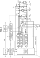
- FIG. 1 is a diagram illustrating a configuration of a switching power supply device according to a first embodiment
- FIG. 2 is a waveform diagram illustrating operations of the switching power supply device according to the first embodiment at startup and steady state;
- FIGS. 3 A to 3 D are diagrams illustrating a startup operation of the switching power supply device according to the first embodiment
- FIGS. 4 A to 4 D are diagrams illustrating a steady-state operation of the switching power supply device according to the first embodiment
- FIG. 5 is a diagram illustrating a configuration of a switching power supply device according to a first modification of the first embodiment
- FIG. 6 is a diagram illustrating a configuration of a switching power supply device according to a second modification of the first embodiment
- FIG. 7 is a diagram illustrating a configuration of a switching power supply device according to a second embodiment
- FIG. 8 is a waveform diagram illustrating a startup operation of the switching power supply device according to the second embodiment
- FIGS. 9 A to 9 D are diagrams illustrating a startup operation of the switching power supply device according to the second embodiment
- FIGS. 10 A to 10 D are diagrams illustrating a steady-state operation of the switching power supply device according to the second embodiment
- FIG. 11 is a diagram illustrating a configuration of a switching power supply device according to a first modification of the second embodiment
- FIG. 12 is a diagram illustrating a configuration of a switching power supply device according to a second modification of the second embodiment
- FIG. 13 is a diagram illustrating a configuration of a switching power supply device according to a third modification of the second embodiment
- FIG. 14 is a diagram illustrating a configuration of a switching power supply device according to a fourth modification of the second embodiment
- FIG. 15 is a diagram illustrating a configuration of a switching power supply device according to a third embodiment
- FIG. 16 is a waveform diagram illustrating a startup operation of the switching power supply device according to the third embodiment.
- FIGS. 17 A to 17 D are diagrams illustrating a startup operation of the switching power supply device according to the third embodiment
- FIG. 18 is a diagram illustrating a configuration of a switching power supply device according to a first modification of the third embodiment
- FIG. 19 is a diagram illustrating a configuration of a switching power supply device according to a second modification of the third embodiment
- FIG. 20 is a diagram illustrating a configuration of a switching power supply device according to a third modification of the third embodiment.
- FIG. 21 is a diagram illustrating a configuration of a switching power supply device according to a fourth modification of the third embodiment.
- the switching power supply device is arranged between an AC power supply and a load circuit, converts the AC power received from the AC power supply into DC power, and outputs the DC power to the load circuit.
- the switching power supply device uses a PFC (Power Factor Correction) circuit in order to convert AC power into DC power while improving the power factor of AC power.
- PFC Power Factor Correction
- the switching power supply device may be configured using a diode bridge, an inductor, a switching element, a diode, and a smoothing capacitor as a PFC circuit, for example.
- a diode bridge can be configured by bridging four diodes. In this configuration, after full-wave rectifying the AC voltage with a diode bridge, energy is repeatedly accumulated and released in the inductor by the switching operation of a switching element, and accordingly, stopping and injection of the current into a smoothing capacitor via the diode are repeated. As a result, the switching power supply device can generate a DC output voltage while bringing the phase of the AC current close to the phase of the AC voltage, and can improve the power factor.
- an inrush current may be generated at the moment when the circuit is connected to the AC power supply at the startup when the supply of the AC power by the AC power supply starts.
- the voltage of the smoothing capacitor is low, so that a steep current can flow through the smoothing capacitor as a transient current, and accordingly, an inrush current can flow through the circuit.
- a configuration is conceivable in which two of the four diodes of the diode bridge are replaced with a thyristor instead of the mechanical relay.
- control is conceivable in which the phase angle of an input voltage is calculated and the thyristor is gate-driven at a predetermined phase angle.
- the switching power supply device tends to complicate the control of the gate drive of the thyristor since the phase angle range to be controlled is calculated in addition to the calculation of the phase angle at startup.
- the control load increases, an operation delay or the like occurs, and the gate drive of the thyristor deviates from an appropriate timing, so that the control accuracy tends to deteriorate.
- the switching power supply device is controlled using the input voltage itself detected at startup, and the thyristor is selectively turned on during the period in which the absolute amplitude value thereof is smaller than a threshold value, thereby simplifying the suppression control of the inrush current.
- a switching power supply device 1 can be configured as a full-bridge-type switching power supply device as illustrated in FIG. 1 .
- FIG. 1 is a diagram illustrating a configuration of the switching power supply device 1 .
- the switching power supply device 1 is arranged between an AC power supply PS and a load circuit LD, converts the AC power received from the AC power supply PS into DC power, and outputs the DC power to the load circuit LD.
- the switching power supply device 1 has input nodes Nin1, Nin2 and output nodes Nout1 and Nout2, and the AC power supply PS may be connected to the input nodes Nin1 and Nin2, and the load circuit LD may be connected to the output nodes Nout1 and Nout2.
- the voltage of the input node Nin1 based on the input node Nin2 is called the input voltage Vin
- the voltage of the output node Nout1 based on the output node Nout2 is called an output voltage Vout.
- the input voltage Vin is an AC voltage
- the output voltage Vout is a DC voltage.
- the switching power supply device 1 gradually increases the output voltage Vout to a predetermined level while monitoring the input voltage Vin and the output voltage Vout.
- the switching power supply device 1 performs a switching operation by the switching element while monitoring the input voltage Vin and the output voltage Vout, and generates an output voltage Vout in a desired voltage range.
- the switching power supply device 1 includes a thyristor SCR1, a thyristor SCR2, a diode D1, a diode D2, an induction element L1, a diode D3, a switching element SW1, a capacitive element C1, a voltage detection unit 2 , a voltage detection unit 3 , and a control circuit 10 .
- the thyristor SCR1, the thyristor SCR2, the diode D1 and the diode D2 are bridge-connected and can function as a diode bridge for full-wave rectifying the AC current from the AC current power supply PS.
- the thyristor SCR1 is electrically connected between the input node Nin1 and the node N1.
- the thyristor SCR1 can function as a rectifying element that rectifies the current in the direction from the input node Nin1 to the node N1 according to the control from the control circuit 10 .
- the anode is connected to the input node Nin1
- the cathode is connected to the node N1
- the gate is connected to the control circuit 10 .
- the thyristor SCR1 is turned on when the control signal of the active level Va1 is received from the control circuit 10 at the gate to function as a rectifying element that rectifies the current from the input node Nin1 to the node N1.
- the thyristor SCR1 is turned off when the control signal of the non-active level Vna1 is received from the control circuit 10 at the gate to electrically disconnect the input node Nin1 from the node N1.
- the control signal of the active level Va1 corresponds to a gate voltage V H1 (for example, 5 V) that turns on the thyristor SCR1.
- V H1 gate voltage
- the control signal of the non-active level Vna1 corresponds to a gate voltage V L1 (for example, 0 V) that turns off the thyristor SCR1.
- V L1 for example, 0 V
- the non-active level Vna1 is based on the cathode potential, and is expressed by the following equation 2 using the cathode potential Vk1 of the thyristor SCR1.
- Vna 1 Vk 1+ V L1 Formula 2
- the thyristor SCR2 is electrically connected between the input node Nin2 and the node N1.
- the thyristor SCR2 can function as a rectifying element that rectifies the current in the direction from the input node Nin2 to the node N1 according to the control from the control circuit 10 .
- the anode is connected to the input node Nin2
- the cathode is connected to the node N1
- the gate is connected to the control circuit 10 .
- the thyristor SCR2 is turned on when the control signal of the active level Va2 is received from the control circuit 10 at the gate to function as a rectifying element that rectifies the current from the input node Nin2 to the node N1.
- the thyristor SCR2 is turned off when the control signal of the non-active level Vna2 is received from the control circuit 10 at the gate to electrically disconnect the input node Nin2 from the node N1.
- the control signal of the active level Va2 corresponds to a gate voltage V H2 (for example, 5 V) that turns on the thyristor SCR2.
- V H2 gate voltage
- the active level Va2 is based on the cathode potential, and is expressed by the following equation 3 assuming that the cathode potential of the thyristor SCR2 is Vk2.
- Va 2 Vk 2+ V H2 Formula 3
- the control signal of the non-active level Vna2 corresponds to a gate voltage V L2 (for example, 0 V) that turns off the thyristor SCR2.
- V L2 for example, 0 V
- the non-active level Vna2 is based on the cathode potential and is expressed by the following equation 4 using the cathode potential Vk2 of the thyristor SCR2.
- Vna 2 Vk 2+ V L2 Formula 4
- the diode D1 is electrically connected between the input node Nin1 and the node N2.
- the cathode is connected to the input node Nin1 and the anode is connected to the node N2.
- the diode D1 functions as a rectifying element that rectifies the current in the direction from the node N2 to the input node Nin1.
- the diode D2 is electrically connected between the input node Nin2 and the node N2.
- the cathode is connected to the input node Nin2 and the anode is connected to the node N2.
- the diode D2 functions as a rectifying element that rectifies the current in the direction from the node N2 to the input node Nin2.
- the induction element L1 is electrically connected between the node N1 and the node N3.
- the induction element L1 is, for example, a coil, one end of which is connected to the node N1 and the other end of which is connected to the node N3.
- the induction element L1 can contribute to the improvement of the power factor of the switching power supply device 1 by accumulating and releasing electromagnetic energy in a steady state.
- the diode D3 is electrically connected between the node N3 and the output node Nout1.
- the anode is connected to the node N3 and the cathode is connected to the output node Nout1 and the capacitive element C1.
- the diode D3 functions as a rectifying element that rectifies the current in the direction from the node N3 to the output node Nout1.
- the switching element SW1 is electrically connected between the node N3 and the output node Nout2.
- the switching element SW1 electrically connects/disconnects the node N3 and the output node Nout2 according to the control from the control circuit 10 .
- the switching element SW1 is, for example, an N-channel MOSFET transistor, in which the source is connected to the node N2, the drain is connected to the node N3, and the gate is connected to the control circuit 10 .
- the transistor electrodes are described as drain, gate, and source on the assumption that the switching element SW1 is an N-channel MOSFET, but when the switching element SW1 is an IGBT (insulated gate-type bipolar transistor), the drain can be read a collector and the source can be read an emitter.
- IGBT insulated gate-type bipolar transistor
- the switching element SW1 is turned on when the control signal of the active level Va3 is received from the control circuit 10 at the gate to electrically connect the node N3 to the output node Nout2.
- the switching element SW1 is turned off when the control signal of the non-active level Vna3 is received from the control circuit 10 at the gate to electrically disconnect the node N3 from the output node Nout2.
- the N-channel MOSFET transistor is provided with a parasitic diode, and the anode side of the parasitic diode is connected to the source and the cathode side is connected to the drain. Therefore, the current can always flow from the source to the drain regardless of whether the control signal received at the gate is an active level or a non-active level.
- the switching element SW1 is an IGBT, no current flows from the node Nout2 to the node N3 because there is no parasitic diode.
- the control signal of the active level Va3 corresponds to a gate voltage V H3 (for example, 15 V) that turns on the switching element SW1.
- V H3 for example, 15 V
- the control signal of the non-active level Vna3 corresponds to a gate voltage V L3 (for example, 0 V) that turns off the switching element SW1.
- the non-active level Vna3 is based on the source potential and is expressed by the following equation 7 using the source potential Vs1 of the switching element SW1.
- Vna 3 Vs 1+ V L3 Formula 7 Since the source of the switching element SW1 is connected to the node N2, the following equation 8 holds when the potential of the node N2 is Vn2.
- Vs 1 Vn 2 Formula 8
- the capacitive element C1 is electrically connected between the output node Nout1 and the output node Nout2.
- the capacitive element C1 is, for example, a smoothing capacitor such as an aluminum electrolytic capacitor, a film capacitor, or a ceramic capacitor, and one end thereof is connected to the output node Nout1 and the other end is connected to the output node Nout2.
- the capacitive element C1 can contribute to the improvement of the power factor of the switching power supply device 1 by discharging and charging the electric charge in a steady state, and can generate an output voltage Vout.
- the voltage detection unit 2 detects the input voltage Vin received via the input node Nin1 and the input node Nin2.
- the voltage detection unit 2 includes a detection node 2 a .
- the detection node 2 a is electrically connected between the input node Nin1 and the thyristor SCR1 and is electrically connected to the control circuit 10 .
- the voltage detection unit 2 transmits the voltage of the detection node 2 a to the control circuit 10 as the detected input voltage Vin.
- the voltage detection unit 3 detects the output voltage Vout output from the output node Nout1 and the output node Nout2 to the load circuit LD.
- the voltage detection unit 3 includes a detection node 3 a .
- the detection node 3 a is electrically connected between the diode D3 and the output node Nout1 and is electrically connected to the control circuit 10 .
- the voltage detection unit 3 transmits the voltage of the detection node 3 a to the control circuit 10 as the detected output voltage Vout.
- the control circuit 10 controls the thyristor SCR1, the thyristor SCR2, and the switching element SW1 according to the input voltage Vin detected by the voltage detection unit 2 and the output voltage Vout detected by the voltage detection unit 3 .
- the control circuit 10 selectively turns on the thyristor SCR1 or the thyristor SCR2 during a period in which the absolute amplitude value of the input voltage Vin is smaller than a threshold value. At this time, the control circuit 10 maintains the switching element SW1 in the off state and does not control the switching operation. Further, the connection to the load circuit LD may be disconnected by turning off a switch LDSW connected between the output node Nout1 and the load circuit LD.
- the control circuit 10 maintains the thyristor SCR1 in the on state while maintaining the thyristor SCR2 and the switching element SW1 in the off state in a first period.
- the first period is a period in which the absolute amplitude value is equal to or less than a first threshold value within the latter half of a first half-cycle of the input voltage at startup.
- the control circuit 10 maintains the thyristor SCR1, the thyristor SCR2, and the switching element SW1 in the off state in a third period.
- the third period is a period within the first half-cycle excluding the first period.
- control circuit 10 maintains the thyristor SCR2 in the on state while maintaining the thyristor SCR1 and the switching element SW1 in the off state in a second period.
- the second period is a period in which the absolute amplitude value is equal to or less than a second threshold value within the latter half of a second half-cycle of the input voltage at startup.
- the second half-cycle is the half-cycle following the first half-cycle.
- the control circuit 10 maintains the thyristor SCR1, the thyristor SCR2, and the switching element SW1 in the off state in a fourth period.
- the fourth period is a period within the second half-cycle excluding the second period.
- the switching power supply device 1 can gradually accumulate electric charges in the capacitive element C1 and gradually increase the output voltage Vout. Therefore, the change of the current transiently flowing through the capacitive element C1 can be moderated, and the inrush current can be suppressed.
- the control circuit 10 ends the startup operation.
- the control circuit 10 controls the switching operation by the switching element SW1 in a state where the load circuit LD is connected (for example, a state where the switch LDSW is maintained on) in the steady state.
- the switching power supply device 1 can generate an output voltage Vout within a desired voltage range.
- the control circuit 10 has a gate drive signal generation function 16, an insulation function 17, an insulation function 18, an insulation function 19, a gate drive function 11, a gate drive function 12, a gate drive function 13, a gate drive power supply function 14, and a gate drive power supply function 15, a capacitive element C11, and a capacitive element C12.
- a DC voltage Vbat (for example, 12 V) held by the battery BT is converted to a DC voltage Vcont1 (for example, 5 V) for control by a DCDC converter CV1 and is supplied to the gate drive signal generation function 16 and the gate drive power supply function 14. Further, the DC voltage Vbat held by the battery BT is converted into a DC voltage Vcont2 (for example, 15 V) for control by the DCDC converter CV2 and is supplied to the gate drive power supply function 15.
- the gate drive signal generation function 16 is a function of generating a gate drive signal to be supplied to the gate drive functions 11 to 13 (for example, based on the ground potential) using the DC voltage Vcont1, and can be implemented as hardware.
- the gate drive signal generation function 16 can be implemented in a digital signal processing circuit by software such as a microcomputer or DSP.
- the gate drive signal generation function 16 generates a gate drive signal GD SCR1 and supplies the same to the gate drive function 11 via the insulation function 17.
- the gate drive signal GD SCR1 is a signal that controls the timing at which the thyristor SCR1 is turned on and off.
- the gate drive signal generation function 16 generates a gate drive signal GD SCR2 and supplies the same to the gate drive function 12 via the insulation function 18.
- the gate drive signal GD SCR2 is a signal that controls the timing at which the thyristor SCR2 is turned on and off.
- the gate drive signal generation function 16 generates the gate drive signal GD SW1 and supplies the same to the gate drive function 13 via the insulation function 19.
- the gate drive signal GD SW1 is a signal that controls the timing at which the switching element SW1 is turned on and off.
- the insulation function 17 electrically insulates the gate drive signal generation function 16 and the gate drive function 11, and transmits the gate drive signal GD SCR1 generated by the gate drive signal generation function 16 to the gate drive function 11.
- the insulation function 18 electrically insulates the gate drive signal generation function 16 and the gate drive function 12, and transmits the gate drive signal GD SCR2 generated by the gate drive signal generation function 16 to the gate drive function 12.
- the insulation function 19 electrically insulates the gate drive signal generation function 16 and the gate drive function 13, and transmits the gate drive signal GD SW1 generated by the gate drive signal generation function 16 to the gate drive function 13.
- the insulation functions 17, 18 and 19 correspond to the gate drive functions 11, 12 and 13, respectively.
- Each of the insulation functions 17 to 19 may have a photocoupler, a magnetic coupler, or a capacitive coupler.
- each of the insulation functions 17 to 19 has a light-emitting element and a light-receiving element coupled optically, causes the light-emitting element to emit light in response to a gate drive signal, causes the light-receiving element to receive the light, and transmits the same to the corresponding gate drive function.
- each of the insulation functions 17 to 19 has a transmission coupler and a reception coupler coupled magnetically, causes the transmission coupler to generate a magnetic field in response to a gate drive signal, causes the reception coupler to generate an induction current in response to the magnetic field, and transmits the same to the corresponding gate drive function.
- a capacitive coupler each of the insulation functions 17 to 19 has a transmitting electrode and a receiving electrode coupled capacitively, causes the transmitting electrode to generate an electric field in response to a gate drive signal, causes the receiving electrode to generate current in response to the electric field, and transmits the same to the corresponding gate drive function.
- the gate drive function 11 is a function for driving the thyristor SCR1 and can be implemented as a hardware circuit.
- the gate drive function 11 can be implemented as an IC provided with a circuit for amplifying current, such as, for example, a push-pull circuit of a transistor.
- the gate drive function 11 generates a control signal CS SCR1 and supplies the same to the gate of the thyristor SCR1 to drive the thyristor SCR1.
- the signal input node is connected to the gate drive signal generation function 16 via the insulation function 17.
- the gate drive function 11 receives the gate drive signal GD SCR1 for the thyristor SCR1 from the gate drive signal generation function 16 via the insulation function 17.
- the power input node is connected to one end of the capacitive element C11 and the gate drive power supply function 14.
- the reference input node is connected to the other end of the capacitive element C11 and the node N1.
- the gate drive function 11 receives the cathode potential Vk1 of the thyristor SCR1 as a reference potential.
- the gate drive function 12 is a function for driving the thyristor SCR2, and can be implemented as a hardware circuit.
- the gate drive function 12 can be implemented as an IC provided with a circuit for amplifying current, such as, for example, a push-pull circuit of a transistor.
- the gate drive function 12 generates a control signal CS SCR2 and supplies the same to the gate of the thyristor SCR2 to drive the thyristor SCR2.
- the signal input node is connected to the gate drive signal generation function 16 via the insulation function 18.
- the gate drive function 12 receives the gate drive signal GD SCR2 for the thyristor SCR2 from the gate drive signal generation function 16 via the insulation function 18.
- the power input node is connected to one end of the capacitive element C11 and the gate drive power supply function 14.
- the reference input node is connected to the other end of the capacitive element C11 and the node N1.
- the gate drive function 12 receives the cathode potential Vk2 of the thyristor SCR2 as a reference potential.
- the gate drive power supply function 14 can be shared by the gate drive function 11 and the gate drive function 12.
- the gate drive power supply function 14 generates a gate drive voltage V SCR and supplies the same to the gate drive function 11 and the gate drive function 12.
- the gate drive voltage V SCR corresponds to the gate voltages V H1 and V H2 that turn on the thyristor SCR1 or thyristor SCR2, and for example, V H1 ⁇ V H2 ⁇ V SCR .
- the gate drive power supply function 14 generates the gate drive voltage V SCR (for example, 5 V) using the voltage Vcont1 and accumulates the gate drive voltage V SCR in the capacitive element C11.
- the gate drive function 11 receives the gate drive voltage V SCR accumulated in the capacitive element C11 at the power input node. At this time, the capacitive element C11 holds the gate drive voltage V SCR When the cathode potential Vk1 of the thyristor SCR1 fluctuates and the potential of the other end of the capacitive element C11 fluctuates, the potential of one end of the capacitive element C11 also fluctuates. As a result, the gate drive function 11 can receive the gate drive voltage V SCR of the active level Va1 which fluctuates according to the fluctuation of the cathode potential Vk1 at the power supply node.
- the gate drive function 11 can generate the control signals CS SCR1 of the active level Va1 and the non-active level Vna1 shown in Equations 1 and 2 according to the gate drive signal GD SCR1 and supply the same to the gate of the thyristor SCR1. That is, the control circuit 10 can control the gate voltage of the thyristor SCR1 so as to be maintained at V H1 or V L1 with reference to the cathode.
- the gate drive function 12 receives the gate drive voltage V SCR accumulated in the capacitive element C11 at the power input node.
- the capacitive element C11 holds the gate drive voltage V SCR
- the cathode potential Vk2 of the thyristor SCR2 fluctuates and the potential of the other end of the capacitive element C11 fluctuates, the potential of one end of the capacitive element C11 also fluctuates.
- the gate drive function 12 can receive the gate drive voltage V SCR of the active level Va2 which fluctuates according to the fluctuation of the cathode potential Vk2 at the power supply node.
- the gate drive function 12 can generate the control signals CS SCR2 of the active level Va2 and the non-active level Vna2 shown in Equations 3 and 4 according to the gate drive signal GD SCR2 and supply the same to the gate of the thyristor SCR2. That is, the control circuit 10 can control the gate voltage of the thyristor SCR2 so as to be maintained at V H2 or V L2 with reference to the cathode.
- the gate drive function 13 is a function of driving the switching element SW1 and can be implemented as a hardware circuit.
- the gate drive function 13 can be implemented as an IC provided with a circuit for amplifying current, such as, for example, a push-pull circuit of a transistor.
- the gate drive function 13 generates a control signal CS SW1 and supplies the same to the gate of the switching element SW1 to drive the switching element SW1.
- the signal input node is connected to the gate drive signal generation function 16 via the insulation function 19.
- the gate drive function 13 receives the gate drive signal GD SW1 for the switching element SW1 from the gate drive signal generation function 16 via the insulation function 19.
- the power input node is connected to one end of the capacitive element C12 and the gate drive power supply function 14.
- the reference input node is connected to the other end of the capacitive element C12 and the node N2.
- the gate drive function 13 receives the source potential Vs1 of the switching element SW1 as a reference potential.
- the gate drive power supply function 15 generates a gate drive voltage V SW and supplies the same to the gate drive function 13.
- the gate drive voltage V SW corresponds to the gate voltage V H3 that turns on the switching element SW1, and for example, V H3 ⁇ V SW .
- the gate drive power supply function 15 generates the gate drive voltage V SW (for example, 15 V) using the voltage Vcont2, and accumulates the gate drive voltage V SW in the capacitive element C12.
- the gate drive function 13 receives the gate drive voltage V SW accumulated in the capacitive element C12 at the power input node. At this time, the capacitive element C12 holds the gate drive voltage V SW .
- the gate drive function 13 can receive the gate drive voltage V SW of the active level Va3 which fluctuates according to the fluctuation of the source potential Vs1 at the power supply node.
- the gate drive function 13 can generate the control signals CS SW1 of the active level Va3 and the non-active level Vna3 shown in Equations 6 and 7 according to the gate drive signal GD SW1 and supply the same to the gate of the switching element SW1. That is, the control circuit 10 can control the gate voltage of the switching element SW1 so as to be maintained at V H3 or V L3 with reference to the source.
- the gate drive power supply functions 14 and 15 may be mounted in a circuit in which an element such as a transformer that generates a voltage and a power supply IC that stabilizes the output voltage using the element as a voltage source are combined in series.
- the insulation functions 17 to 19 and the gate drive functions 11 to 13 may be implemented as an IC in which the corresponding sets are integrated.
- the insulation functions 17 to 19, the gate drive functions 11 to 13, and the gate drive power supply functions 14 and 15 may be mounted using a pulse transformer that transmits high-frequency pulses as a component in which the corresponding sets are integrated.
- FIG. 2 is a waveform diagram illustrating the operations of the switching power supply device 1 at startup and steady state.
- FIGS. 3 A to 3 D are diagrams illustrating the startup operation of the switching power supply device 1 .
- FIGS. 4 A to 4 D are diagrams illustrating the steady-state operation of the switching power supply device 1 .
- the input voltage Vin is an AC voltage and changes in a sinusoidal shape around a reference potential (for example, 0 V). If the amplitude higher than the reference potential is called a positive amplitude and the amplitude lower than the reference potential is called a negative amplitude, the input voltage Vin becomes the positive amplitude at the odd-numbered half-cycles T 1 , T 3 , T 5 , and T 7 counting from the timing t1, and becomes the negative amplitude at the even-numbered half-cycles T 2 , T 4 , T 6 , and T 8 .
- a reference potential for example, 0 V
- the control circuit 10 maintains the gate voltages of the thyristor SCR1, the thyristor SCR2, and the switching element SW1 at V L1 V L2 , and V L3 , respectively, in response to the tendency of the absolute amplitude value of the input voltage Vin to increase.
- the control circuit 10 compares the absolute amplitude value of the input voltage Vin with the threshold value Vth1 when the absolute amplitude value of the input voltage Vin tends to decrease.
- the control circuit 10 maintains the gate voltages of the thyristor SCR1, the thyristor SCR2, and the switching element SW1 at V L2 , V L2 , and V L3 , respectively, in response to the absolute amplitude value of the input voltage Vin being larger than the threshold value Vth1.
- the thyristor SCR1, the thyristor SCR2, and the switching element SW1 are each maintained in the off state, no current flows from the AC power supply PS, and the output voltage Vout generated by the capacitive element C1 is maintained at the initial value V0 ( ⁇ 0 V).
- the control circuit 10 maintains the gate voltages of the thyristor SCR2 and the switching element SW1 at V L2 and V L3 , respectively, in response to the absolute amplitude value of the input voltage Vin reaching the threshold value Vth1, and changes the gate voltage of V L1 of the thyristor SCR1 to V H1 .
- the control circuit 10 maintains the gate voltages of the thyristor SCR2 and the switching element SW1 at V L2 and V L3 , respectively, in response to the absolute amplitude value of the input voltage Vin being equal to or less than the threshold value Vth1, and maintains the gate voltage of the thyristor SCR1 at V H1 .
- the period T 12 is a period in which the absolute amplitude value of the input voltage Vin is equal to or less than the threshold value Vth1 within the latter half of the half-cycle T 1 .
- the period T 11 is the period within the half-cycle T1 excluding the period T 12 .
- the control circuit 10 maintains the gate voltages of the thyristor SCR1, the thyristor SCR2, and the switching element SW1 at V L1 , V L2 , and V L3 , respectively, in response to the tendency of the absolute amplitude value of the input voltage Vin to increase.
- the control circuit 10 compares the absolute amplitude value of the input voltage Vin with the threshold value Vth2 when the absolute amplitude value of the input voltage Vin tends to decrease.
- the control circuit 10 maintains the gate voltages of the thyristor SCR1, the thyristor SCR2, and the switching element SW1 at V L1 , V L2 , and V L3 , respectively, in response to the absolute amplitude value of the input voltage Vin being larger than the threshold value Vth2.
- the thyristor SCR1, the thyristor SCR2, and the switching element SW1 are each maintained in the off state, no current flows from the AC power supply PS, and the output voltage Vout generated by the capacitive element C1 is maintained at V1.
- the control circuit 10 maintains the gate voltages of the thyristor SCR1 and the switching element SW1 at V L1 and V L3 , respectively, in response to the absolute amplitude value of the input voltage Vin reaching the threshold value Vth2, and changes the gate voltage of the thyristor SCR2 from V L2 to V H2 .
- the control circuit 10 maintains the gate voltages of the thyristor SCR1 and the switching element SW1 at V L1 and V L3 , respectively, in response to the absolute amplitude value of the input voltage Vin being equal to or less than the threshold value Vth2, and maintains the gate voltage of the thyristor SCR2 at V H2 .
- the period T 22 is a period in which the absolute amplitude value of the input voltage Vin is equal to or less than the threshold value Vth2 within the latter half of the half-cycle T 2 .
- the threshold value Vth2 is larger than the threshold value Vth1. Therefore, the length of the period T 22 is longer than the length of the period T 12 .
- the period T 21 is the period excluding the period T 22 in the half-cycle T 2 .
- the control circuit 10 maintains the gate voltages of the thyristor SCR1, the thyristor SCR2, and the switching element SW1 at V L1 V L2 , and V L3 , respectively, in response to the tendency of the absolute amplitude value of the input voltage Vin to increase.
- the control circuit 10 compares the absolute amplitude value of the input voltage Vin with the threshold value Vth3.
- the control circuit 10 maintains the gate voltages of the thyristor SCR1, the thyristor SCR2, and the switching element SW1 at V L2 , V L2 , and V L3 , respectively, in response to the absolute amplitude value of the input voltage Vin being larger than the threshold value Vth3.
- the thyristor SCR1, the thyristor SCR2, and the switching element SW1 are each maintained in the off state, no current flows from the AC power supply PS, and the output voltage Vout generated by the capacitive element C1 is maintained at V2.
- the control circuit 10 maintains the gate voltages of the thyristor SCR2 and the switching element SW1 at V L2 and V L3 , respectively, in response to the absolute amplitude value of the input voltage Vin reaching the threshold value Vth3, and changes the gate voltage of the thyristor SCR1 from V L1 to V H1 .
- the control circuit 10 maintains the gate voltages of the thyristor SCR2 and the switching element SW1 at V L2 and V L3 , respectively, in response to the absolute amplitude value of the input voltage Vin being equal to or less than the threshold value Vth3, and maintains the gate voltage of the thyristor SCR1 at V H1 .
- the control circuit 10 maintains the gate voltages of the thyristor SCR2 and the switching element SW1 at V L2 and V L3 , respectively, in response to the absolute amplitude value of the input voltage Vin being equal to or less than the threshold value Vth3, and maintains the gate voltage of the thyristor SCR1 at V H1 .
- the period T 32 is a period in which the absolute amplitude value of the input voltage Vin is equal to or less than the threshold value Vth3 within the latter half of the half-cycle T 3 .
- the threshold value Vth3 is larger than the threshold value Vth2. Therefore, the length of the period T 32 is longer than the length of the period T 22 .
- the period T 31 is the period within the half-cycle T 3 excluding the period T 32 .
- the control circuit 10 maintains the gate voltages of the thyristor SCR1, the thyristor SCR2, and the switching element SW1 at V L2 , V L2 , and V L3 , respectively, in response to the tendency of the absolute amplitude value of the input voltage Vin to increase.
- the control circuit 10 compares the absolute amplitude value of the input voltage Vin with the threshold value Vth4.
- the control circuit 10 maintains the gate voltages of the thyristor SCR1, the thyristor SCR2, and the switching element SW1 at V L2 , V L2 , and V L3 , respectively, in response to the absolute amplitude value of the input voltage Vin being larger than the threshold value Vth4.
- the thyristor SCR1, the thyristor SCR2, and the switching element SW1 are each maintained in the off state, no current flows from the AC power supply PS, and the output voltage Vout generated by the capacitive element C1 is maintained at V3.
- the control circuit 10 maintains the gate voltages of the thyristor SCR1 and the switching element SW1 at V L1 and V L3 , respectively, in response to the absolute amplitude value of the input voltage Vin reaching the threshold value Vth4, and changes the gate voltage of the thyristor SCR2 from V L2 to V H2 .
- the control circuit 10 maintains the gate voltages of the thyristor SCR1 and the switching element SW1 at V L1 and V L3 , respectively, in response to the absolute amplitude value of the input voltage Vin being equal to or less than the threshold value Vth4, and maintains the gate voltage of the thyristor SCR2 at V H2 .
- the period T 42 is a period in which the absolute amplitude value of the input voltage Vin is equal to or less than the threshold value Vth4 within the latter half of the half-cycle T 4 .
- the threshold value Vth4 is larger than the threshold value Vth3. Therefore, the length of the period T 42 is longer than the length of the period T 32 .
- the period T 41 is the period within the half-cycle T 4 excluding the period T 42 .
- the control circuit 10 ends the startup operation and switches to the steady-state operation when the output voltage Vout reaches the desired voltage V 4 .
- the output voltage Vout reaches the desired voltage V 4 when the half-cycle occurs four times is described, but the number of half-cycles is not limited to this. This operation may be repeated until the output voltage Vout reaches the desired voltage V4.
- the control circuit 10 maintains the gate voltages of the thyristor SCR1 and the thyristor SCR2 at V H1 and V L2 , respectively, when the timing is within the odd-numbered half-cycle T 5 . Further, the control circuit 10 alternately switches the gate voltage of the switching element SW1 between V H3 and V L3 . As a result, the thyristor SCR2 is maintained in the off state, and the operations of FIGS. 4 A and 4 B are alternately repeated. That is, as illustrated in FIG.
- the load circuit LD Since the load circuit LD is connected, the current is supplied from the capacitive element C1 to the load LD regardless of whether the switching element SW1 is turned on or off, so that the output voltage Vout always gradually decreases. Therefore, in detail, an operation in which the voltage Vout of the capacitive element C1 gradually decreases during the period in which the switching element SW1 is turned on, and rapidly increases during the period in which the switching element SW1 is turned off is repeated.
- the control circuit 10 maintains the gate voltages of the thyristor SCR1 and the thyristor SCR2 at V L1 and V H2 , respectively, when the timing is within the even-numbered half-cycle T 6 . Further, the control circuit 10 alternately switches the gate voltage of the switching element SW1 between V H3 and V L3 . As a result, the thyristor SCR1 is maintained in the off state, and the operations of FIGS. 4 C and 4 D are alternately repeated. That is, as illustrated in FIG.
- the load circuit LD Since the load circuit LD is connected, the current is supplied from the capacitive element C1 to the load LD regardless of whether the switching element SW1 is turned on or off, so that the output voltage Vout always gradually decreases. Therefore, in detail, an operation in which the voltage Vout of the capacitive element C1 gradually decreases during the period in which the switching element SW1 is turned on, and rapidly increases during the period in which the switching element SW1 is turned off is repeated.
- the operation in the odd-numbered half-cycle T 7 is the same as the operation in the half-cycle T 5 in the period of timings t11 to t12
- the operation in the even-numbered half-cycle T 8 is the same as the operation in the half-cycle T 6 in the period of timings t12 to t13.
- the switching power supply device 1 performs control using the input voltage Vin itself detected at startup, and selectively turns on the thyristor SCR1 or SCR2 during a period in which the absolute amplitude value is smaller than the threshold value.
- the control for suppressing the inrush current at startup can be simplified as compared with the case of performing complicated control such as calculating the phase angle of the input voltage.
- the configuration of the control circuit 10 for performing the control can be simplified.
- a switching power supply device 101 may have a configuration in which the insulation function 19 (see FIG. 1 ) is omitted, as illustrated in FIG. 5 .
- FIG. 5 is a diagram illustrating a configuration of the switching power supply device 101 according to the first modification of the first embodiment.
- the gate drive signal generation function 16 can generate the gate drive signal GD SW1 based on the source of the switching element SW1, and can align the signal reference of the gate drive signal generation function 16 and the gate drive function 12.
- the gate drive function 12 can be electrically connected to the gate drive signal generation function 16, and the gate drive signal GD SW1 can be directly supplied from the gate drive signal generation function 16 to the gate drive function 12. That is, since the insulation function 19 (see FIG. 1 ) can be omitted, the configuration of a control circuit 110 can be further simplified.
- a switching power supply device 201 may further include a noise filter 220 as illustrated in FIG. 6 .
- FIG. 6 is a diagram illustrating the configuration of the switching power supply device 201 according to the second modification of the first embodiment, and the illustration of the control circuit is omitted for simplification.
- the noise filter 220 is electrically connected between the input node Nin1 and the input node Nin2, and the thyristor SCR1, the thyristor SCR2, the diode D1 and the diode D2.
- the noise filter 220 includes common mode coils L2 and L3, line-to-line capacitors C2 and C3, and line-to-ground capacitors C4, C5, C6, and C7.
- One set of ends of the common mode coils L2 and L3 are connected to the input nodes Nin1 and Nin2, respectively, and the other set of ends are connected to the nodes between the thyristors SCR1 and SCR2 and the diodes D1 and D2, respectively.
- the common mode coils L2 and L3 are configured to be wound in phase with each other on the core, and cancel the magnetic fluxes of the current flowing through the coils and attenuate the common mode noise.
- One set of ends of the line-to-line capacitors C2 and C3 are connected to the line connecting the input node Nin1 and the thyristor SCR1, and the other set of ends are connected to the line connecting the input node Nin2 and the thyristor SCR2.
- the line-to-line capacitors C2 and C3 can bypass noise between lines and attenuate normal mode noise.
- One set of ends of the line-to-ground capacitors C4 and C5 are connected to the line connecting the input node Nin1 and the thyristor SCR1, and the other set of ends are connected to the ground potential.
- the line-to-ground capacitors C4 and C5 can bypass noise to the ground potential and attenuate common mode noise.
- One set of ends of the line-to-ground capacitors C6 and C7 are connected to the line connecting the input node Nin2 and the thyristor SCR2, and the other set of ends are connected to the ground potential.
- the line-to-ground capacitors C6 and C7 can bypass noise to the ground potential and attenuate common mode noise.
- the switching power supply device 201 can further suppress the radiation of noise to the outside and can reduce the influence of the noise from the outside since it further includes the noise filter 220 .
- a full-bridge-type switching power supply device is illustrated, but in the second embodiment, a bridgeless-type switching power supply device having no diode bridge is illustrated.
- a switching power supply device 301 as illustrated in FIG. 7 , the diodes D1 and D2 are omitted, and an induction element L11, thyristors SCR11 and SCR12, switching elements SW11 and SW12, and a control circuit 310 are provided instead of the induction element L1, the thyristors SCR1 and SCR2, the switching element SW1, and the control circuit 10 (see FIG. 1 ).
- the induction element L11 is electrically connected between the input node Nin1 and the node N11.
- the induction element L11 is, for example, a coil, one end of which is connected to the input node Nin1 and the other end of which is connected to the node N11.
- the thyristor SCR11 is electrically connected between the input node Nin2 and the output node Nout1.
- the cathode is connected to the output node Nout1 via the node N13
- the anode is connected to the input node Nin2, and the gate is connected to the control circuit 10 .
- the thyristor SCR11 is turned on when the control signal of the active level Va11 is received from the control circuit 10 at the gate, and is turned off when the control signal of the non-active level Vna11 is received at the gate.
- the control signal of the active level Va11 corresponds to a gate voltage VH 11 (for example, 5 V) that turns on the thyristor SCR11.
- VH 11 for example, 5 V
- the control signal of the non-active level Vna11 corresponds to a gate voltage V L11 (for example, 0 V) that turns off the thyristor SCR11.
- V L11 for example, 0 V
- the non-active level Vna11 is based on the cathode potential and is expressed by the following equation 10 using the cathode potential Vk11 of the thyristor SCR11.
- Vna 11 Vk 11+ V L11 Formula 10
- the thyristor SCR12 is electrically connected between the input node Nin2 and the output node Nout2.
- the cathode is connected to the input node Nin2
- the anode is connected to the output node Nout2
- the gate is connected to the control circuit 10 .
- the thyristor SCR12 is turned on when the control signal of the active level Va12 is received from the control circuit 10 at the gate, and is turned off when the control signal of the non-active level Vna12 is received at the gate.
- the control signal of the active level Va12 corresponds to a gate voltage V H12 (for example, 5 V) that turns on the thyristor SCR12.
- V H12 for example, 5 V
- the control signal of the non-active level Vna12 corresponds to a gate voltage V L12 (for example, 0 V) that turns off the thyristor SCR12.
- V L12 for example, 0 V
- the non-active level Vna12 is based on the cathode potential and is expressed by the following equation 12 using the cathode potential Vk12 of the thyristor SCR12.
- Vna 12 Vk 12+ V L12 Formula 12
- the switching element SW11 is electrically connected between the node N11 and the output node Nout1.
- the switching element SW11 is, for example, an N-channel MOSFET transistor, in which the source is connected to the node N11, the drain is connected to the output node Nout1, and the gate is connected to the control circuit 10 .
- the switching element SW11 is turned on when the control signal of the active level Va13 is received from the control circuit 10 at the gate, and is turned off when the control signal of the non-active level Vna13 is received at the gate.
- the control signal of the active level Va13 corresponds to a gate voltage V H13 (for example, 15 V) that turns on the switching element SW11.
- V H13 for example, 15 V
- the control signal of the non-active level Vna13 corresponds to a gate voltage V L13 (for example, 0 V) that turns off the switching element SW11.
- V L13 for example, 0 V
- the non-active level Vna13 is based on the source potential and is expressed by the following equation 14 using the source potential Vs11 of the switching element SW11.
- Vna 13 Vs 11+ V L13 Formula 14
- the switching element SW12 is electrically connected between the node N11 and the output node Nout2.
- the switching element SW12 is, for example, an N-channel MOSFET transistor, in which the source is connected to the output node Nout2 via the node N14, the drain is connected to the node N11, and the gate is connected to the control circuit 10 .
- the switching element SW12 is turned on when the control signal of the active level Va14 is received from the control circuit 10 at the gate, and is turned off when the control signal of the non-active level Vna14 is received at the gate.
- the control signal of the active level Va14 corresponds to a gate voltage V H14 (for example, 15 V) that turns on the switching element SW12.
- V H14 for example, 15 V
- the control signal of the non-active level Vna14 corresponds to a gate voltage V L14 (for example, 0 V) that turns off the switching element SW12.
- the non-active level Vna14 is based on the source potential and is expressed by the following equation 16 using the source potential Vs12 of the switching element SW12.
- Vna 14 Vs 12+ V L14 Formula 16
- the control circuit 310 controls the thyristor SCR11, the thyristor SCR12, the switching element SW11, and the switching element SW12 according to the input voltage Vin detected by the voltage detection unit 2 and the output voltage Vout detected by the voltage detection unit 3 .
- the control circuit 310 selectively turns on the thyristor SCR11 or the thyristor SCR12 during a period in which the absolute amplitude of the input voltage Vin is smaller than the threshold value. For example, the control circuit 310 maintains the thyristor SCR12 and the switching element SW11 in the on state while maintaining the thyristor SCR11 and the switching element SW12 in the off state in a first period.
- the first period is a period in which the absolute amplitude value is equal to or less than the first threshold value within the latter half of a first half-cycle of the input voltage Vin at startup.
- the control circuit 310 maintains the thyristor SCR11, the thyristor SCR12, the switching element SW11, and the switching element SW12 in the off state in a third period.
- the third period is a period within the first half-cycle excluding the first period.
- the control circuit 310 maintains the thyristor SCR11 and the switching element SW12 in the on state while maintaining the thyristor SCR12 and the switching element SW11 in the off state in a second period.
- the second period is a period in which the absolute amplitude value is equal to or less than the second threshold value within the latter half of the second half-cycle following the first half-cycle of the input voltage Vin at startup.
- the control circuit 310 maintains the thyristor SCR11, the thyristor SCR12, the switching element SW12, and the switching element SW11 in the off state in a fourth period.
- the fourth period is a period within the second half-cycle excluding the second period.
- the references of the control signals of the thyristor SCR11, the thyristor SCR12, the switching element SW11, and the switching element SW12 are the potential of the node N13, the potential of the node N12, the potential of the node N11, and the potential of the node N14, respectively, which are different from each other. Therefore, the control circuit 310 is configured to separately generate control signals for the thyristor SCR11, the thyristor SCR12, the switching element SW11, and the switching element SW12.
- control circuit 310 has a gate drive signal generation function 319, insulation functions 315, 316, 317, and 318, gate drive functions 311, 312, 313, and 314, gate drive power supply functions 321, 322, 323, and 324, and capacitive elements C21, C22, C23, and C24.
- a DC voltage Vbat (for example, 12 V) held by the battery BT is converted to a DC voltage Vcont1 (for example, 5 V) for control by the DCDC converter CV1 and is supplied to the gate drive signal generation function 319 and the gate drive power supply functions 321 and 322. Further, the DC voltage Vbat held by the battery BT is converted into a DC voltage Vcont2 (for example, V) for control by the DCDC converter CV2 and is supplied to the gate drive power supply functions 323 and 324.
- Vbat for example, 12 V
- Vcont1 for example, 5 V
- Vcont2 for example, V
- the gate drive signal generation function 319 generates a gate drive signal GD SCR11 and supplies the same to the gate drive function 311 via the insulation function 315.
- the gate drive signal generation function 319 generates a gate drive signal GD SCR12 and supplies the same to the gate drive function 312 via the insulation function 316.
- the gate drive signal generation function 319 generates a gate drive signal GD SW11 and supplies the same to the gate drive function 313 via the insulation function 317.
- the gate drive signal generation function 319 generates a gate drive signal GD SW12 and supplies the same to the gate drive function 314 via the insulation function 318.
- the insulation function 315 electrically insulates the gate drive signal generation function 319 and the gate drive function 311, and transmits the gate drive signal GD SCR11 generated by the gate drive signal generation function 319 to the gate drive function 311.
- the insulation function 316 electrically insulates the gate drive signal generation function 319 and the gate drive function 312, and transmits the gate drive signal GD SCR12 generated by the gate drive signal generation function 319 to the gate drive function 312.
- the insulation function 317 electrically insulates the gate drive signal generation function 319 and the gate drive function 313, and transmits the gate drive signal GD SW11 generated by the gate drive signal generation function 319 to the gate drive function 313.
- the insulation function 318 electrically insulates the gate drive signal generation function 319 and the gate drive function 314, and transmits the gate drive signal GD SW12 generated by the gate drive signal generation function 319 to the gate drive function 314.
- the gate drive function 311 is a function for driving the thyristor SCR11.
- the signal input node is connected to the gate drive signal generation function 319 via the insulation function 315
- the power input node is connected to one end of the capacitive element C21 and the gate drive power supply function 321
- the reference input node is connected to the other end of the capacitive element C21 and the node N13.
- the gate drive function 312 is a function for driving the thyristor SCR12.
- the signal input node is connected to the gate drive signal generation function 319 via the insulation function 316
- the power input node is connected to one end of the capacitive element C22 and the gate drive power supply function 322
- the reference input node is connected to the other end of the capacitive element C22 and the node N12.
- the gate drive function 313 is a function for driving the switching element SW11.
- the signal input node is connected to the gate drive signal generation function 319 via the insulation function 317
- the power input node is connected to one end of the capacitive element C23 and the gate drive power supply function 323
- the reference input node is connected to the other end of the capacitive element C23 and the node N11.
- the gate drive function 314 is a function for driving the switching element SW12.
- the signal input node is connected to the gate drive signal generation function 319 via the insulation function 318
- the power input node is connected to one end of the capacitive element C24 and the gate drive power supply function 324
- the reference input node is connected to the other end of the capacitive element C24 and the node N14.
- the gate drive power supply function 321 generates the gate drive voltage V SCR11 and supplies the same to the gate drive function 311.
- the gate drive voltage V SCR11 corresponds to a gate voltage V H11 that turns on the thyristor SCR11, and for example, V H11 ⁇ V SCR11 .
- the gate drive power supply function 321 generates a gate drive voltage V SCR11 (for example, 5 V) using the voltage Vcont1, and accumulates the gate drive voltage V SCR11 in the capacitive element C21.
- V SCR11 for example, 5 V
- the gate drive function 311 receives the gate drive voltage V SCR11 accumulated in the capacitive element C21 at the power input node.
- the gate drive function 311 can generate the control signals CS SCR11 of the active level Va11 and the non-active level Vna11 shown in Equations 9 and 10 according to the gate drive signal GD SCR11 and supply the same to the gate of the thyristor SCR11. That is, the control circuit 310 can control the gate voltage of the thyristor SCR11 so as to be maintained at V H11 or V L11 with reference to the cathode.
- the gate drive power supply function 322 generates the gate drive voltage V SCR12 and supplies the same to the gate drive function 312.
- the gate drive voltage V SCR12 corresponds to the gate voltage V H12 that turns on the thyristor SCR12, and for example V H12 ⁇ V SCR12 .
- the gate drive power supply function 322 generates the gate drive voltage V SCR12 (for example, 5 V) using the voltage Vcont1 and accumulates the gate drive voltage V SCR12 in the capacitive element C22.
- the gate drive function 312 receives the gate drive voltage V SCR12 accumulated in the capacitive element C22 at the power input node.
- the gate drive function 312 can generate the control signals CS SCR12 of the active level Va12 and the non-active level Vna12 shown in Equations 11 and 12 according to the gate drive signal GD SCR12 and supply the same to the gate of the thyristor SCR12. That is, the control circuit 310 can control the gate voltage of the thyristor SCR12 so as to be maintained at V H12 or V L12 with reference to the cathode.
- the gate drive power supply function 323 generates the gate drive voltage V SW11 and supplies the same to the gate drive function 313.
- the gate drive voltage V SW11 corresponds to the gate voltage V H13 that turns on the switching element SW11, and for example, V H13 ⁇ V SW11 .
- the gate drive power supply function 323 generates the gate drive voltage V SW11 (for example, 15 V) using the voltage Vcont2, and accumulates the gate drive voltage V SW11 in the capacitive element C23.
- the gate drive function 313 receives the gate drive voltage V SW11 accumulated in the capacitive element C23 at the power input node.
- the gate drive function 313 can generate the control signals CS SW11 of the active level Va13 and the non-active level Vna13 shown in Equations 13 and 14 according to the gate drive signal GD SW11 and supply the same to the gate of the switching element SW11. That is, the control circuit 310 can control the gate voltage of the switching element SW11 so as to be maintained at V H13 or V L13 with reference to the source.
- the gate drive power supply function 324 generates the gate drive voltage V SW12 and supplies the same to the gate drive function 314.
- the gate drive voltage V SW12 corresponds to the gate voltage V H14 that turns on the switching element SW12, and for example, V H14 ⁇ V SW12
- the gate drive power supply function 324 generates the gate drive voltage V SW12 (for example, 15 V) using the voltage Vcont2, and accumulates the gate drive voltage V SW12 in the capacitive element C24.
- the gate drive function 314 receives the gate drive voltage V SW12 accumulated in the capacitive element C24 at the power input node.
- the gate drive function 314 can generate the control signals CS SW12 of the active level Va14 and the non-active level Vna14 shown in Equations 15 and 16 according to the gate drive signal GD SW12 and supply the same to the gate of the switching element SW12. That is, the control circuit 310 can control the gate voltage of the switching element SW12 so as to be maintained at V H14 or V L14 with reference to the source.
- FIG. 8 is a waveform diagram illustrating the startup operation of the switching power supply device 301 .
- FIGS. 9 A to 9 D are diagrams illustrating the startup operation of the switching power supply device 301 .
- the control circuit 310 maintains at least the gate voltages of the thyristor SCR12 and the switching element SW12 at V L12 and V L14 , respectively, in response to the tendency of the absolute amplitude value of the input voltage Vin to increase.
- the gate voltages of the thyristor SCR11 and the switching element SW11 may be V L11 , V L13 or V H11 , V H13 , respectively.
- the control circuit 310 compares the absolute amplitude value of the input voltage Vin with the threshold value Vth1 when the absolute amplitude value of the input voltage Vin tends to decrease.
- the control circuit 310 maintains at least the gate voltages of the thyristor SCR12 and the switching element SW12 at V L12 and V L14 , respectively, in response to the absolute amplitude value of the input voltage Vin being larger than the threshold value Vth1.
- the gate voltages of the thyristor SCR11 and the switching element SW11 may be V L11 , V L13 or V H11 , V H13 , respectively.
- the control circuit 310 changes the gate voltage of the thyristor SCR12 from V L12 to V H12 in response to the absolute amplitude value of the input voltage Vin reaching the threshold value Vth1.
- the gate voltage of the switching element SW12 may be maintained at V L14
- the gate voltage of the thyristor SCR11 may be V L11 or V H11 .
- the control circuit 310 maintains the gate voltage of the switching element SW12 at V L14 in response to the absolute amplitude value of the input voltage Vin being equal to or less than the threshold value Vth1, and maintains the gate voltages of the thyristor SCR12 and the switching element SW11 at V H12 and V H13 , respectively.
- the control circuit 310 maintains the gate voltage of the switching element SW12 at V L14 in response to the absolute amplitude value of the input voltage Vin being equal to or less than the threshold value Vth1, and maintains the gate voltages of the thyristor SCR12 and the switching element SW11 at V H12 and V H13 , respectively.
- the control circuit 310 maintains at least the gate voltages of the thyristor SCR11 and the switching element SW11 at V L11 and V L13 , respectively, in response to the tendency of the absolute amplitude value of the input voltage Vin to increase.
- the gate voltages of the thyristor SCR12 and the switching element SW12 may be V L12 , V L14 or V H12 , V H14 , respectively.
- the control circuit 310 compares the absolute amplitude value of the input voltage Vin with the threshold value Vth2 when the absolute amplitude value of the input voltage Vin tends to decrease.
- the control circuit 310 maintains the gate voltages of the thyristor SCR11 and the switching element SW11 at V L11 and V L13 , respectively, in response to the absolute amplitude value of the input voltage Vin being larger than the threshold value Vth2.
- the thyristor SCR11 and the switching element SW11 are each maintained in the off state, no current flows from the AC power supply PS, and the output voltage Vout generated by the capacitive element C1 is maintained at V1.
- the gate voltages of the thyristor SCR12 and the switching element SW12 may be V L12 , V L14 or V H12 , V H14 , respectively.
- the control circuit 310 changes the gate voltage of the thyristor SCR11 from V L11 to V H11 in response to the absolute amplitude value of the input voltage Vin reaching the threshold value Vth2.
- the gate voltage of the switching element SW11 may be maintained at V L13
- the gate voltage of the thyristor SCR12 may be V L12 or V H12 .
- the control circuit 310 maintains at least the gate voltages of the thyristor SCR11 and the switching element SW12 at V H11 and V H14 , respectively, in response to the absolute amplitude value of the input voltage Vin being equal to or less than the threshold value Vth2.
- the control circuit 310 maintains at least the gate voltages of the thyristor SCR11 and the switching element SW12 at V H11 and V H14 , respectively, in response to the absolute amplitude value of the input voltage Vin being equal to or less than the threshold value Vth2.
- the switching element SW12 is an N-channel MOSFET
- the gate voltage may be maintained at V L14 because the parasitic diode is provided as described in the first embodiment. This is because the current flows through the parasitic diode.
- the same operation as in the period T 11 of the timings t21 to t22 is performed.
- the same operation as in the period T 12 of the timings t22 to t23 is performed.
- the same operation as in the period T 21 of the timings t23 to t24 is performed.
- the same operation as in the period T 22 of the timings t24 to t25 is performed.
- the control circuit 310 ends the startup operation and switches to the steady-state operation when the output voltage Vout reaches the desired voltage V 4 .
- the steady-state operation substantially the same operation as that of the first embodiment can be performed.
- control circuit 310 maintains the gate voltages of the thyristor SCR11 and the thyristor SCR12 at V L11 and V H12 , respectively, when the timing is within the odd-numbered half-cycle T 5 . Further, the control circuit 310 alternately switches the gate voltage of the switching element SW12 between V H14 and V L14 and alternately switches the gate voltage of the switching element SW11 between V L13 and V H13 . The gate voltages of the switching element SW12 and the switching element SW11 do not become V H14 and V H13 at the same time.
- the thyristor SCR11 is maintained in the off state
- the thyristor SCR12 is maintained in the on state
- the switching element SW12 is turned on/off
- the switching element SW11 is turned off/on, whereby the operations of FIGS. 10 A and 10 B are repeated alternately. That is, as illustrated in FIG. 10 A , current flows in the path of AC power supply PS ⁇ induction element L11 ⁇ switching element SW12 ⁇ thyristor SCR12 ⁇ AC power supply PS, and electromagnetic energy is accumulated in the induction element L11. Subsequently, as illustrated in FIG.
- the control circuit 310 maintains the gate voltages of the thyristor SCR11 and the thyristor SCR12 at V H11 and V L12 , respectively, when the timing is within the even-numbered half-cycle T 6 . Further, the control circuit 310 alternately switches the gate voltage of the switching element SW11 between V H13 and V L13 and at the same time alternately switches the gate voltage of the switching element SW12 between V L14 and V H14 . The gate voltages of the switching element SW11 and the switching element SW12 do not become V H13 and V H14 at the same time.
- the thyristor SCR12 is maintained in the off state, the thyristor SCR11 is maintained in the on state, the switching element SW11 is turned on/off, and the switching element SW12 is turned off/on, whereby the operation of FIGS. 10 C and 10 C is repeated alternately. That is, as illustrated in FIG. 10 C , current flows in the path of AC power supply PS ⁇ thyristor SCR11 ⁇ switching element SW11 ⁇ induction element L11 ⁇ AC power supply PS, and electromagnetic energy is accumulated in the induction element L11. Subsequently, as illustrated in FIG.
- the operation in the odd-numbered half-cycle T 7 is the same as the operation in the half-cycle T 5 in the period of timings t11 to t12
- the operation in the even-numbered half-cycle T 8 is the same as the operation in the half-cycle T 6 in the period of timings t12 to t13.
- the switching power supply device 301 performs control using the input voltage Vin itself detected at startup, and selectively turns on the thyristor SCR11 or SCR12 during the period in which the absolute amplitude value is smaller than the threshold value.
- the control for suppressing the inrush current at startup can be simplified as compared with the case of performing complicated control such as calculating the phase angle of the input voltage.
- control for suppressing the inrush current at startup can be simplified as compared with the case of performing complicated control such as calculating the phase angle of the input voltage, so that the configuration of the control circuit 310 can be simplified.
- the switching power supply device 301 is a bridgeless type, the number of elements of the diode, thyristor, and transistor through which the current path passes can be reduced as compared with the switching power supply device 1 of the first embodiment. For example, in FIGS. 3 B and 3 D , the number of elements through which the current path passes is three, whereas in FIGS. 9 B and 9 D , the number of elements through which the current path passes is only two. As a result, the switching power supply device 301 can reduce the power loss due to elements.
- a switching power supply device 401 has a configuration in which the gate drive power supply function is shared for a plurality of gate drive functions.
- FIG. 11 is a diagram illustrating a configuration of the switching power supply device 401 according to the first modification of the second embodiment.
- a diode D21 is added between the gate drive power supply function 321 and the gate drive function 311 and a diode D22 is added between the gate drive power supply function 323 and the gate drive function 313.
- the cathode is connected to the gate drive function 311 and the anode is connected to the gate drive power supply function 321 and the gate drive function 312.
- the gate drive power supply function 321 is connected to the gate drive function 311 via the diode D21, and is connected to the gate drive function 312 without via the diode D21.
- the cathode is connected to the gate drive function 313, and the anode is connected to the gate drive power supply function 323 and the gate drive function 314.
- the gate drive power supply function 323 is connected to the gate drive function 313 via the diode D22, and is connected to the gate drive function 314 without via the diode D22.
- the diodes D21 and D22 can prevent the current from flowing back from one set of ends of the capacitive elements C21 and C23 toward the gate drive power supply functions 321 and 323 when the potential at one set of ends of the capacitive elements C21 and C23 becomes higher than the gate drive voltage supplied from the gate drive power supply functions 321 and 323 to the gate drive function. That is, the gate drive power supply function 321 can be shared with the gate drive functions 311 and 312, and the gate drive power supply function 323 can be shared with the gate drive functions 313 and 314. As a result, the gate drive power supply functions 322 and 324 (see FIG. 18 ) can be omitted, so that the configuration of the control circuit 410 can be further simplified.
- a switching power supply device 501 may have a configuration in which the insulation function 318 (see FIG. 7 ) is omitted as illustrated in FIG. 12 .
- FIG. 12 is a diagram illustrating a configuration of the switching power supply device 501 according to the second modification of the second embodiment. For example, in the configuration illustrated in FIG. 7 , a line for electrically connecting the node N14 to the gate drive function 314 and the gate drive signal generation function 319 is added, and the other end of the capacitive element C24 is connected to the line.
- the gate drive signal generation function 319 can generate the gate drive signal GD SW12 based on the source of the switching element SW12, and align the signal references of the gate drive signal generation function 319 and the gate drive function 314. Therefore, as illustrated in FIG. 12 , the gate drive function 314 can be electrically connected to the gate drive signal generation function 319, and the gate drive signal GD SW12 can be directly supplied from the gate drive signal generation function 319 to the gate drive function 314. That is, since the insulation function 318 (see FIG. 18 ) can be omitted, the configuration of a control circuit 510 can be further simplified.
- a switching power supply device 601 may have a configuration in which the insulation function 318 (see FIG. 11 ) is omitted as illustrated in FIG. 13 .
- FIG. 13 is a diagram illustrating a configuration of the switching power supply device 601 according to the third modification of the second embodiment. For example, in the configuration illustrated in FIG. 11 , a line for electrically connecting the node N14 to the gate drive function 314 and the gate drive signal generation function 319 is added, and the other end of the capacitive element C24 is connected to the line.
- the gate drive signal generation function 319 can generate the gate drive signal GD SW12 based on the source of the switching element SW12, and align the signal references of the gate drive signal generation function 319 and the gate drive function 314. Therefore, as illustrated in FIG. 13 , the gate drive function 314 can be electrically connected to the gate drive signal generation function 319, and the gate drive signal GD SW12 can be directly supplied from the gate drive signal generation function 319 to the gate drive function 314. That is, since the insulation function 318 (see FIG. 11 ) can be omitted, the configuration of a control circuit 610 can be further simplified.
- a switching power supply device 701 may further include a noise filter 220 as illustrated in FIG. 14 .
- FIG. 14 is a diagram illustrating the configuration of the switching power supply device 701 according to the fourth modification of the second embodiment, and the illustration of the control circuit is omitted for simplification.
- a noise filter 220 is electrically connected between the input node Nin1 and the input node Nin2 and the induction element L11, the thyristor SCR11, the thyristor SCR12, the switching element SW11 and the switching element SW12.
- the noise filter 220 includes common mode coils L2 and L3, line-to-line capacitors C2 and C3, and line-to-ground capacitors C4, C5, C6, and C7.
- One end of the common mode coil L2 is connected to the input node Nin1, and the other end is connected to the node between the switching element SW11 and the switching element SW12 via the induction element L11.
- One end of the common mode coil L3 is connected to the input node Nin2, and the other end is connected to the node between the thyristor SCR11 and the thyristor SCR12.
- the common mode coils L2 and L3 are configured to be wound in phase with each other on the core, and cancel the magnetic fluxes of the current flowing through the coils and attenuate the common mode noise.
- One set of ends of the line-to-line capacitors C2 and C3 are connected to the line connecting the input node Nin1 and the induction element L11, and the other set of ends are connected to the line connecting the input node Nin2 and the thyristors SCR11 and SCR12.
- the line-to-line capacitors C2 and C3 can bypass noise between lines and attenuate normal mode noise.
- One set of ends of the line-to-ground capacitors C4 and C5 are connected to the line connecting the input node Nin1 and the induction element L11, and the other set of ends are connected to the ground potential.
- the line-to-ground capacitors C4 and C5 can bypass noise to the ground potential and attenuate common mode noise.
- One set of ends of the line-to-ground capacitors C6 and C7 are connected to the line connecting the input node Nin2 and the thyristors SCR11 and SCR12, and the other set of ends are connected to the ground potential.
- the line-to-ground capacitors C6 and C7 can bypass noise to the ground potential and attenuate common mode noise.
- the switching power supply device 701 can suppress the radiation of noise to the outside and can reduce the influence of the noise from the outside since it further includes the noise filter 220 .
- the second embodiment illustrates a configuration in which the nodes that serve as the reference for the gate voltages of the plurality of thyristors and the plurality of switching elements are different from each other, but in the third embodiment, a configuration in which the nodes that serve as the reference for the gate voltages of the plurality of thyristors and the plurality of switching elements are shared will be illustrated.
- a switching power supply device 801 includes an induction element L21, thyristors SCR21 and SCR22, switching elements SW21 and SW22, and a control circuit 810 instead of the induction element L11, the thyristors SCR11 and SCR12, the switching elements SW11 and SW12, and the control circuit 310 (see FIG. 7 ).
- the induction element L21 is electrically connected between the input node Nin1 and the node N21. One end of the induction element L21 is connected to the input node Nin1 and the other end is connected to the node N21.
- the thyristor SCR21 is electrically connected between the node N21 and the output node Nout2.
- the cathode is connected to the node N21
- the anode is connected to the output node Nout2
- the gate is connected to the control circuit 810 .
- the thyristor SCR22 is electrically connected between the input node Nin2 and the output node Nout2.
- the cathode is connected to the input node Nin2 via the node N22
- the anode is connected to the output node Nout2
- the gate is connected to the control circuit 810 .
- the switching element SW21 is electrically connected between the node N21 and the output node Nout1.
- the switching element SW21 is, for example, an N-channel MOSFET transistor, in which the source is connected to the node N21, the drain is connected to the output node Nout1, and the gate is connected to the control circuit 810 .
- the switching element SW22 is electrically connected between the input node Nin2 and the output node Nout1.
- the switching element SW22 is, for example, an N-channel MOSFET transistor, in which the source is connected to the input node Nin2 via the node N22, the drain is connected to the output node Nout1, and the gate is connected to the control circuit 810 .
- the thyristor SCR21 and the switching element SW21 share a common node that serves as a reference for the gate voltage. Both the cathode of the thyristor SCR21 and the source of the switching element SW21 are connected to the node N21.
- the thyristor SCR22 and the switching element SW22 have a common node that serves as a reference for the gate voltage. Both the cathode of the thyristor SCR22 and the source of the switching element SW22 are connected to the node N22.
- the reference of the control signal of the thyristor SCR21 and the reference of the control signal of the switching element SW21 can be made common, and the reference of the control signal of the thyristor SCR22 and the reference of the control signal of the switching element SW22 can be made common, so that the configuration of the control circuit 810 can be simplified.
- the gate drive power supply function 321, the gate drive power supply function 322, the capacitive element C21, and the capacitive element C22 are omitted from the control circuit 310 (see FIG. 7 ).
- One end of the capacitive element C23 is commonly connected to the power supply node of the gate drive function 311 and the power supply node of the gate drive function 313, and the other end is commonly connected to the reference node of the gate drive function 311 and the reference node of the gate drive function 313.
- One end of the capacitive element C23 is connected to the gate drive power supply function 323, and the other end is connected to the node N21.
- One end of the capacitive element C24 is commonly connected to the power supply node of the gate drive function 312 and the power supply node of the gate drive function 314, and the other end is commonly connected to the reference node of the gate drive function 312 and the reference node of the gate drive function 314.
- One end of the capacitive element C24 is connected to the gate drive power supply function 324, and the other end is connected to the node N22.
- control circuit 810 controls the thyristor SCR21, the thyristor SCR22, the switching element SW21, and the switching element SW22 according to the input voltage Vin detected by the voltage detection unit 2 and the output voltage Vout detected by the voltage detection unit 3 .
- the content of control by the control circuit 810 is the same as that of the second embodiment.
- FIG. 16 is a waveform diagram illustrating the startup operation of the switching power supply device 801 .
- FIGS. 17 A to 17 D are diagrams illustrating the startup operation of the switching power supply device 801 .
- the same operation as the period T 11 of the timings t21 to t22 is performed.
- the thyristor SCR22 and the switching element SW22 are maintained in the off state in the period T 11 , as illustrated in FIG. 17 A , no current flows from the AC power supply PS, and the output voltage Vout generated by the capacitive element C1 is maintained at the initial value V0 ( ⁇ 0 V).
- the thyristor SCR21 and the switching element SW21 are shown in the off state in FIG. 17 A , they may be in the on state.
- the same operation as in the period T 12 of the timings t32 to t23 is performed. That is, the thyristor SCR22 is maintained in the on state, and the switching element SW22 is maintained in the off state.
- the period T 12 as illustrated in FIG. 17 B , current flows in the path of AC power supply PS ⁇ induction element L21 ⁇ switching element SW21 ⁇ capacitive element C1 ⁇ thyristor SCR22 ⁇ AC power supply PS, electric charges are accumulated in the capacitive element C1, and the output voltage Vout generated by the capacitive element C1 rises from V0 to V1. It is desirable to maintain the switching element SW21 in the ON state from the viewpoint of circuit efficiency.
- the same operation as in the period T 21 of the timings t33 to t24 is performed.
- the thyristor SCR21 and the switching element SW21 are maintained in the off state in the period T 21 , as illustrated in FIG. 17 C , no current flows from the AC power supply PS, and the output voltage Vout generated by the capacitive element C1 is maintained at V1.
- the thyristor SCR22 and the switching element SW22 are shown in the off state in FIG. 17 C , they may be in the on state.
- the same operation as that of the period T 22 of the timings t24 to t25 is performed. That is, the thyristor SCR21 is maintained in the on state and the switching element SW21 is maintained in the off state.
- the period T 22 as illustrated in FIG. 17 D , current flows in the path of AC power supply PS ⁇ switching element SW22 ⁇ capacitive element C1 ⁇ thyristor SCR21 ⁇ induction element L21 ⁇ AC power supply PS, electric charges are accumulated in the capacitive element C1, and the output voltage Vout generated by the capacitive element C1 rises from V1 to V2. It is desirable to maintain the switching element SW22 in the ON state from the viewpoint of circuit efficiency.
- the same operation as in the period T 11 of the timings t31 to t32 is performed.
- the same operation as in the period T 12 of the timings t32 to t33 is performed.
- the same operation as in the period T 21 of the timings t33 to t34 is performed.
- the same operation as in the period T 22 of the timings t34 to t35 is performed.
- the control circuit 810 ends the startup operation and switches to the steady-state operation when the output voltage Vout reaches the desired voltage V 4 .
- the steady-state operation substantially the same operation as that of the first embodiment can be performed.
- the switching power supply device 801 performs control using the input voltage Vin itself detected at startup, and selectively turns on the thyristor SCR21 or SCR22 during a period in which the absolute amplitude value is smaller than the threshold value.
- the control for suppressing the inrush current at startup can be simplified as compared with the case of performing complicated control such as calculating the phase angle of the input voltage.
- the configuration of the control circuit 810 for performing the control can be simplified.
- the switching power supply device 801 is a bridgeless type, the number of elements of the diode, thyristor, and transistor through which the current path passes can be reduced as compared with the switching power supply device 1 of the first embodiment. For example, in FIGS. 3 B and 3 D , the number of elements through which the current path passes is three, whereas in FIGS. 17 B and 17 D , the number of elements through which the current path passes is only two. As a result, the switching power supply device 801 can reduce the power loss due to elements.
- a switching power supply device 901 has a configuration in which the gate drive power supply function is shared for a plurality of gate drive functions.
- FIG. 18 is a diagram illustrating a configuration of the switching power supply device 901 according to the first modification of the third embodiment.
- a diode D31 is added between the gate drive power supply function 323 and the gate drive functions 311 and 313.
- the cathode is connected to the gate drive functions 311 and 313, and the anode is connected to the gate drive power supply function 323 and the gate drive functions 312 and 314.
- the gate drive power supply function 323 is connected to the gate drive functions 311 and 313 via the diode D31, and is connected to the gate drive functions 312 and 314 without via the diode D31.
- the diode D31 can prevent the current from flowing back from one end of the capacitive element C23 to the gate drive power supply function 323 when the potential at one end of the capacitive element C23 becomes higher than the gate drive voltage supplied from the gate drive power supply function 323 to the gate drive functions 312 and 314. That is, since the gate drive power supply function 324 (see FIG. 15 ) can be omitted, the configuration of the control circuit 910 can be further simplified.
- a switching power supply device 1001 may have a configuration in which the insulation functions 316 and 318 (see FIG. 15 ) are omitted as illustrated in FIG. 19 .
- FIG. 19 is a diagram illustrating a configuration of the switching power supply device 1001 according to the second modification of the third embodiment. For example, in the configuration illustrated in FIG. 15 , a line for electrically connecting the node N22 to the gate drive functions 312 and 314 and the gate drive signal generation function 319 is added, and the other end of the capacitive element C24 is connected to the line.
- the gate drive signal generation function 319 can generate the gate drive signal GD SCR22 based on the cathode of the thyristor SCR22, and the signal references of the gate drive signal generation function 319 and the gate drive function 312 can be aligned. Therefore, as illustrated in FIG. 19 , the gate drive function 312 can be electrically connected to the gate drive signal generation function 319, and the gate drive signal GD SCR22 can be directly supplied from the gate drive signal generation function 319 to the gate drive function 312. Similarly, the gate drive signal generation function 319 can generate the gate drive signal GD SW22 based on the source of the switching element SW22, and the signal references of the gate drive signal generation function 319 and the gate drive function 314 can be aligned.
- the gate drive function 314 can be electrically connected to the gate drive signal generation function 319, and the gate drive signal GD SW12 can be directly supplied from the gate drive signal generation function 319 to the gate drive function 314. That is, since the insulation functions 316 and 318 (see FIG. 15 ) can be omitted, the configuration of a control circuit 1010 can be further simplified.
- a switching power supply device 1101 may have a configuration in which the insulation functions 316 and 318 (see FIG. 18 ) are omitted as illustrated in FIG. 20 .
- FIG. 20 is a diagram illustrating a configuration of the switching power supply device 1101 according to the third modification of the third embodiment. For example, in the configuration illustrated in FIG. 18 , a line for electrically connecting the node N22 to the gate drive functions 312 and 314 and the gate drive signal generation function 319 is added, and the other end of the capacitive element C24 is connected to the line.
- the gate drive signal generation function 319 can generate the gate drive signal GD SCR22 based on the cathode of the thyristor SCR22, and the signal references of the gate drive signal generation function 319 and the gate drive function 312 can be aligned. Therefore, as illustrated in FIG. 20 , the gate drive function 312 can be electrically connected to the gate drive signal generation function 319, and the gate drive signal GD SCR22 can be directly supplied from the gate drive signal generation function 319 to the gate drive function 312. Similarly, the gate drive signal generation function 319 can generate the gate drive signal GD SW22 based on the source of the switching element SW22, and the signal references of the gate drive signal generation function 319 and the gate drive function 314 can be aligned.
- the gate drive function 314 can be electrically connected to the gate drive signal generation function 319, and the gate drive signal GD SW22 can be directly supplied from the gate drive signal generation function 319 to the gate drive function 314. That is, since the insulation functions 316 and 318 (see FIG. 18 ) can be omitted, the configuration of a control circuit 1110 can be further simplified.
- a switching power supply device 1201 may further include a noise filter 220 as illustrated in FIG. 21 .
- FIG. 21 is a diagram illustrating the configuration of the switching power supply device 1201 according to the fourth modification of the third embodiment, and the illustration of the control circuit is omitted for simplification.
- a noise filter 220 is electrically connected between the input node Nin 1 and the input node Nin2 and the induction element L21, the switching element SW21, and the switching element SW22.
- the noise filter 220 includes common mode coils L2 and L3, line-to-line capacitors C2 and C3, and line-to-ground capacitors C4, C5, C6, and C7.
- One end of the common mode coil L2 is connected to the input node Nin 1 , and the other end is connected to the switching element SW21 via the induction element L21.
- One end of the common mode coil L3 is connected to the input node Nin2, and the other end is connected to the switching element SW22.
- the common mode coils L2 and L3 are configured to be wound in phase with each other on the core, and cancel the magnetic fluxes of the current flowing through the coils and attenuate the common mode noise.
- One set of ends of the line-to-line capacitors C2 and C3 are connected to a line connecting the input node Nin1 and the induction element L21, and the other set of ends are connected to a line connecting the input node Nin2 and the switching element SW22.
- the line-to-line capacitors C2 and C3 can bypass noise between lines and attenuate normal mode noise.
- One set of ends of the line-to-ground capacitors C4 and C5 are connected to the line connecting the input node Nin1 and the induction element L21, and the other set of ends are connected to the ground potential.
- the line-to-ground capacitors C4 and C5 can bypass noise to the ground potential and attenuate common mode noise.
- One set of ends of the line-to-ground capacitors C6 and C7 are connected to the line connecting the input node Nin2 and the source of the watering element SW22, and the other set of ends are connected to the ground potential.
- the line-to-ground capacitors C6 and C7 can bypass noise to the ground potential and attenuate common mode noise.
- the switching power supply device 1201 can suppress the radiation of noise to the outside and reduce the influence of the noise from the outside since it further includes the noise filter 220 .
- the inrush current can be suppressed by simple control.
Landscapes
- Engineering & Computer Science (AREA)
- Power Engineering (AREA)
- Power Conversion In General (AREA)
- Rectifiers (AREA)
Abstract
Description
Va1=Vk1+V H1 Formula 1
Vna1=Vk1+V L1 Formula 2
Va2=Vk2+V H2 Formula 3
Vna2=Vk2+V L2 Formula 4
Vk1=Vk2=
Va3=Vs1+V H3 Formula 6
Vna3=Vs1+V L3 Formula 7
Since the source of the switching element SW1 is connected to the node N2, the following equation 8 holds when the potential of the node N2 is Vn2.
Vs1=Vn2 Formula 8
The capacitive element C1 is electrically connected between the output node Nout1 and the output node Nout2. The capacitive element C1 is, for example, a smoothing capacitor such as an aluminum electrolytic capacitor, a film capacitor, or a ceramic capacitor, and one end thereof is connected to the output node Nout1 and the other end is connected to the output node Nout2. The capacitive element C1 can contribute to the improvement of the power factor of the switching
V H1 ≈V H2 ≈V SCR.
V H3 ≈V SW.
Va11=Vk11+V H11 Formula 9
Vna11=Vk11+V L11 Formula 10
Va12=Vk12+V H12 Formula 11
Vna12=Vk12+V L12 Formula 12
Va13=Vs11+V H13 Formula 13
Vna13=Vs11+V L13 Formula 14
Va14=Vs12+V H14 Formula 15
Vna14=Vs12+V L14 Formula 16
The
V H11 ≈V SCR11.
V H12 ≈V SCR12.
V H13 ≈V SW11.
V H14 ≈V SW12
The gate drive
Claims (19)
Priority Applications (1)
| Application Number | Priority Date | Filing Date | Title |
|---|---|---|---|
| US18/453,836 US12231037B2 (en) | 2021-02-10 | 2023-08-22 | Switching power supply device |
Applications Claiming Priority (4)
| Application Number | Priority Date | Filing Date | Title |
|---|---|---|---|
| JP2021-020213 | 2021-02-10 | ||
| JP2021020213A JP7518596B2 (en) | 2021-02-10 | 2021-02-10 | Switching Power Supply Unit |
| US17/667,324 US11770068B2 (en) | 2021-02-10 | 2022-02-08 | Switching power supply device |
| US18/453,836 US12231037B2 (en) | 2021-02-10 | 2023-08-22 | Switching power supply device |
Related Parent Applications (1)
| Application Number | Title | Priority Date | Filing Date |
|---|---|---|---|
| US17/667,324 Continuation US11770068B2 (en) | 2021-02-10 | 2022-02-08 | Switching power supply device |
Publications (2)
| Publication Number | Publication Date |
|---|---|
| US20230396156A1 US20230396156A1 (en) | 2023-12-07 |
| US12231037B2 true US12231037B2 (en) | 2025-02-18 |
Family
ID=82704770
Family Applications (2)
| Application Number | Title | Priority Date | Filing Date |
|---|---|---|---|
| US17/667,324 Active 2042-02-08 US11770068B2 (en) | 2021-02-10 | 2022-02-08 | Switching power supply device |
| US18/453,836 Active US12231037B2 (en) | 2021-02-10 | 2023-08-22 | Switching power supply device |
Family Applications Before (1)
| Application Number | Title | Priority Date | Filing Date |
|---|---|---|---|
| US17/667,324 Active 2042-02-08 US11770068B2 (en) | 2021-02-10 | 2022-02-08 | Switching power supply device |
Country Status (2)
| Country | Link |
|---|---|
| US (2) | US11770068B2 (en) |
| JP (1) | JP7518596B2 (en) |
Families Citing this family (3)
| Publication number | Priority date | Publication date | Assignee | Title |
|---|---|---|---|---|
| JP7518596B2 (en) * | 2021-02-10 | 2024-07-18 | パナソニックオートモーティブシステムズ株式会社 | Switching Power Supply Unit |
| FR3126823A1 (en) * | 2021-09-08 | 2023-03-10 | Stmicroelectronics (Tours) Sas | voltage converter |
| US12362662B2 (en) | 2023-05-30 | 2025-07-15 | Stmicroelectronics International N.V. | Commutation assistance by controlling the shape of the current wave in a bidirectional totem pole converter |
Citations (8)
| Publication number | Priority date | Publication date | Assignee | Title |
|---|---|---|---|---|
| US5202819A (en) | 1991-06-13 | 1993-04-13 | Samsung Electronics Co., Ltd. | Capacitor input type rectifier having a circuit for preventing inrush current |
| JP2015033170A (en) | 2013-07-31 | 2015-02-16 | ニチコン株式会社 | Bridgeless power-supply circuit |
| US20150131343A1 (en) | 2013-11-08 | 2015-05-14 | Det International Holding Limited | Resistorless precharging |
| US20180166910A1 (en) | 2016-12-09 | 2018-06-14 | Delta Electronics (Tailand) Public Company Limited | Charging system and method thereof |
| US10124680B1 (en) | 2017-06-28 | 2018-11-13 | Lear Corporation | Methods and systems for pre-charging on-board charger of vehicle |
| JP2021002983A (en) | 2019-06-24 | 2021-01-07 | ルネサスエレクトロニクス株式会社 | Semiconductor device |
| US20210336533A1 (en) | 2020-04-27 | 2021-10-28 | Stmicroelectronics (Tours) Sas | Discharge of an ac capacitor using totem-pole power factor correction (pfc) circuitry |
| US11770068B2 (en) * | 2021-02-10 | 2023-09-26 | Panasonic Intellectual Property Management Co., Ltd. | Switching power supply device |
-
2021
- 2021-02-10 JP JP2021020213A patent/JP7518596B2/en active Active
-
2022
- 2022-02-08 US US17/667,324 patent/US11770068B2/en active Active
-
2023
- 2023-08-22 US US18/453,836 patent/US12231037B2/en active Active
Patent Citations (12)
| Publication number | Priority date | Publication date | Assignee | Title |
|---|---|---|---|---|
| US5202819A (en) | 1991-06-13 | 1993-04-13 | Samsung Electronics Co., Ltd. | Capacitor input type rectifier having a circuit for preventing inrush current |
| JPH05122939A (en) | 1991-06-13 | 1993-05-18 | Samsung Electron Co Ltd | Capacitor input type rectifying smoother with inrush current preventer |
| JP2015033170A (en) | 2013-07-31 | 2015-02-16 | ニチコン株式会社 | Bridgeless power-supply circuit |
| US20150131343A1 (en) | 2013-11-08 | 2015-05-14 | Det International Holding Limited | Resistorless precharging |
| EP3349343A1 (en) | 2013-11-08 | 2018-07-18 | DET International Holding Limited | Resistorless precharging |
| US20180166910A1 (en) | 2016-12-09 | 2018-06-14 | Delta Electronics (Tailand) Public Company Limited | Charging system and method thereof |
| JP2018102117A (en) | 2016-12-09 | 2018-06-28 | デルタ エレクトロニクス (タイ) パブリック コンパニー リミテッドDelta Electronics (Thailand) Public Company Limited | Charging system and method |
| US10124680B1 (en) | 2017-06-28 | 2018-11-13 | Lear Corporation | Methods and systems for pre-charging on-board charger of vehicle |
| JP2021002983A (en) | 2019-06-24 | 2021-01-07 | ルネサスエレクトロニクス株式会社 | Semiconductor device |
| US11139749B2 (en) | 2019-06-24 | 2021-10-05 | Renesas Electronics Corporation | Semiconductor device |
| US20210336533A1 (en) | 2020-04-27 | 2021-10-28 | Stmicroelectronics (Tours) Sas | Discharge of an ac capacitor using totem-pole power factor correction (pfc) circuitry |
| US11770068B2 (en) * | 2021-02-10 | 2023-09-26 | Panasonic Intellectual Property Management Co., Ltd. | Switching power supply device |
Non-Patent Citations (1)
| Title |
|---|
| Japanese Notice of Reasons for Refusal dated May 7, 2024, for the corresponding Japanese Patent Application No. 2021-020213, 5 pages. (With English Machine Translation). |
Also Published As
| Publication number | Publication date |
|---|---|
| JP2022122759A (en) | 2022-08-23 |
| US20220255453A1 (en) | 2022-08-11 |
| US20230396156A1 (en) | 2023-12-07 |
| US11770068B2 (en) | 2023-09-26 |
| JP7518596B2 (en) | 2024-07-18 |
Similar Documents
| Publication | Publication Date | Title |
|---|---|---|
| US12231037B2 (en) | Switching power supply device | |
| US8040702B2 (en) | DC/DC power converting apparatus | |
| US9985533B2 (en) | Control circuit having adaptive blanking time and method for providing the same | |
| US9929661B2 (en) | Switching power supply apparatus | |
| US20100302808A1 (en) | Power source apparatus | |
| EP3758209A1 (en) | Semiconductor device | |
| JP7095784B2 (en) | Switching power supply | |
| US11984813B2 (en) | Synchronous rectification control system and method for quasi-resonant flyback converter | |
| CN102447394A (en) | Flyback converter with an adaptively controlled rectifier arrangement | |
| US8305785B2 (en) | Power source apparatus | |
| CN107294405B (en) | System controller and method for regulating power converters | |
| US11689113B2 (en) | Control circuit of flyback circuit | |
| KR102143254B1 (en) | Pwm controlling apparatus for flyback converter | |
| US20190386574A1 (en) | Power supply and power supply unit | |
| CN105471231A (en) | Flyback AC-DC conversion circuit and flyback voltage converter | |
| KR102409677B1 (en) | Boost converter with boosting and decoupling operation using single inductor | |
| CN110061612B (en) | Power supply control circuit and method | |
| WO2020243871A1 (en) | Converter, charging system and method of manufacturing the converter | |
| US10033262B2 (en) | Gate voltage control device | |
| US12451793B2 (en) | Charging system | |
| US12445050B2 (en) | Voltage converter with reduced inductive energy conversion | |
| JP2022138041A (en) | Switching power supply device | |
| US11502606B2 (en) | Direct-current (DC) voltage conversion device | |
| CN104426226B (en) | Switched-mode power supply with modular construction | |
| JP2020022313A (en) | Switching power supply circuit and power conversion device having the same |
Legal Events
| Date | Code | Title | Description |
|---|---|---|---|
| FEPP | Fee payment procedure |
Free format text: ENTITY STATUS SET TO UNDISCOUNTED (ORIGINAL EVENT CODE: BIG.); ENTITY STATUS OF PATENT OWNER: LARGE ENTITY |
|
| STPP | Information on status: patent application and granting procedure in general |
Free format text: DOCKETED NEW CASE - READY FOR EXAMINATION |
|
| AS | Assignment |
Owner name: PANASONIC AUTOMOTIVE SYSTEMS CO., LTD., JAPAN Free format text: ASSIGNMENT OF ASSIGNORS INTEREST;ASSIGNOR:PANASONIC INTELLECTUAL PROPERTY MANAGEMENT CO., LTD.;REEL/FRAME:066709/0727 Effective date: 20240207 |
|
| STPP | Information on status: patent application and granting procedure in general |
Free format text: NON FINAL ACTION MAILED |
|
| STPP | Information on status: patent application and granting procedure in general |
Free format text: RESPONSE TO NON-FINAL OFFICE ACTION ENTERED AND FORWARDED TO EXAMINER |
|
| STPP | Information on status: patent application and granting procedure in general |
Free format text: NOTICE OF ALLOWANCE MAILED -- APPLICATION RECEIVED IN OFFICE OF PUBLICATIONS |
|
| STPP | Information on status: patent application and granting procedure in general |
Free format text: PUBLICATIONS -- ISSUE FEE PAYMENT VERIFIED |
|
| STCF | Information on status: patent grant |
Free format text: PATENTED CASE |