US12228754B2 - Electronic structure for representing freeform optical surfaces in optical design software - Google Patents
Electronic structure for representing freeform optical surfaces in optical design software Download PDFInfo
- Publication number
- US12228754B2 US12228754B2 US16/896,079 US202016896079A US12228754B2 US 12228754 B2 US12228754 B2 US 12228754B2 US 202016896079 A US202016896079 A US 202016896079A US 12228754 B2 US12228754 B2 US 12228754B2
- Authority
- US
- United States
- Prior art keywords
- axis
- optical surface
- departure
- freeform
- optical
- Prior art date
- Legal status (The legal status is an assumption and is not a legal conclusion. Google has not performed a legal analysis and makes no representation as to the accuracy of the status listed.)
- Active, expires
Links
Images


Classifications
-
- G—PHYSICS
- G02—OPTICS
- G02B—OPTICAL ELEMENTS, SYSTEMS OR APPARATUS
- G02B5/00—Optical elements other than lenses
- G02B5/08—Mirrors
- G02B5/10—Mirrors with curved faces
-
- G—PHYSICS
- G02—OPTICS
- G02B—OPTICAL ELEMENTS, SYSTEMS OR APPARATUS
- G02B27/00—Optical systems or apparatus not provided for by any of the groups G02B1/00 - G02B26/00, G02B30/00
- G02B27/0012—Optical design, e.g. procedures, algorithms, optimisation routines
-
- G—PHYSICS
- G02—OPTICS
- G02B—OPTICAL ELEMENTS, SYSTEMS OR APPARATUS
- G02B27/00—Optical systems or apparatus not provided for by any of the groups G02B1/00 - G02B26/00, G02B30/00
- G02B27/0025—Optical systems or apparatus not provided for by any of the groups G02B1/00 - G02B26/00, G02B30/00 for optical correction, e.g. distorsion, aberration
- G02B27/0068—Optical systems or apparatus not provided for by any of the groups G02B1/00 - G02B26/00, G02B30/00 for optical correction, e.g. distorsion, aberration having means for controlling the degree of correction, e.g. using phase modulators, movable elements
Definitions
- the present disclosure relates to freeform optical surfaces.
- an optical subassembly often include one or more freeform optical surface and/or mirror elements. Selecting the shapes (also commonly referred to as figures) of the individual surfaces of a freeform optical surface or mirror elements is an important step in the design process. Historically, surface figures for applications like cameras were primarily restricted to be a portion of a sphere as they are significantly easier to manufacture and test than non-spherical surfaces.
- FIG. 1 depicts an example of an unobstructed mirror system.
- FIG. 2 depicts a schematic representation of a base surface together with an additional departure to give a total surface figure for a surface in an optical subassembly.
- FIG. 3 depicts a representation of a base surface represented by an off-axis section of a conic, in accordance with one embodiment of the present invention.
- FIG. 4 depicts a schematic representation of a base surface plus additional departure, where the departure is applied in a direction parallel to the surface normal at or near the center of the used-portion of the surface, in accordance with one embodiment of the present invention.
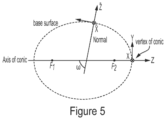
- FIG. 5 depicts a schematic illustration of parameters for specifying an off-axis conic, in accordance with one embodiment of the present invention.
- FIG. 6 depicts a flowchart of various processes used during the design and manufacture of an integrated circuit in accordance with some embodiments of the present disclosure.
- FIG. 7 depicts an abstract diagram of an example computer system in which embodiments of the present disclosure may operate.
- the representation should be stable as the system is optimized and the parameters that represent the surface figure are modified.
- the representation should facilitate a straightforward determination of the ease with which the surface can be manufactured and tested.
- the representation should provide degrees of freedom necessary to correct the aberrations in the system.
- the first is essential for successful design of optical subassemblies. If a surface representation cannot be used successfully with modern optimization algorithms in existing freeform optical surface design packages, then the ability of the freeform optical surface designer to use such surfaces in their design is severely hampered.
- the second enables a freeform optical surface designer to incorporate constraints into the design and optimization process that ensure surface figures in the final design meet two goals: 1) the imaging and packaging requirements are met, and 2) the surfaces can be manufactured and tested.
- the third property is important to obtain the most benefit in the design from a freeform surface. From the standpoint of aberration theory, when rotational-symmetry is broken, there is an increase in the number of aberrations that can be present in the system. Having degrees of freedom in the surface figure that can be varied independently to correct the various aberrations is advantageous when designing systems that break rotational-symmetry.
- aspects of the present disclosure relate to an optical structure that includes an off-axis optical surface and a departure module.
- the off-axis optical surface may be an off-axis conic optical surface and may receive the departure along a substantially perpendicular direction.
- Embodiments of the present invention provide a freeform surface in at least two parts that include a base surface together with a deviation (or departure) in surface height and slope from the base surface. It is advantageous if the base surface is of a form that is easy to fabricate and/or test, so that the challenges to the fabrication and testing of the surface are posed only by the (typically small) deviations from the base surface. It is furthermore advantageous if the base surface, by itself, provides at least an approximate solution to the optical design problem, so that the deviations that are required from the base surface remain small.
- the base surface may be specified by a relatively simple surface representation that is one of a spherical, aspheric, or off-axis conic. One common class of base surface is a conic section of revolution.
- the second part of the surface representation is the deviation (or departure) from the base surface. It is this deviation that provides the additional degrees of freedom to give a truly “freeform” surface.
- This departure from the base surface can be specified in a number of ways. For example, sets of polynomials, such as Zernike polynomials or Forbes Freeform Q-polynomials, have been proposed, although other basis functions could be used.
- the specific departure that is needed for a surface itself depends on both the application and the details about which surface in an optical subassembly is being considered for a freeform. In some embodiments, the departure itself is determined via an automated optimization process in which the coefficients are allowed to vary in order to determine the departure that gives optimal performance for the application at hand.
- the surface has an underlying axis of rotational symmetry, and in existing approaches, the departure is added to the base surface along the direction of this axis.
- This is represented schematically in cross-section in FIG. 2 .
- the solid portion 10 of the base conic is the part of the conic that is illuminated (as represented by the dashed-rays that have been drawn between F 1 and F 2 , the two foci of the conic).
- the departure section 20 is to be added to the base conic, and curved shape 30 represents the sum of the solid portion 10 and the departure section 20 .
- curved shape 30 represents the total freeform surface that results from the base surface 10 and the added departure 20 .
- the small arrows 40 in FIG. 2 represent the departure that is added to the base surface shown at a discrete set of points. These are all parallel to the axis of the conic and signify that the departure is added in the direction of the axis of the conic.
- the departure may be represented by a set of basis functions that allow an arbitrary surface to be described provided the surface is continuous and smooth.
- FIG. 3 illustrates an off-axis conic optical surface.
- the set of basis functions are commonly represented as a set of polynomials that can be of various forms.
- Two common sets of basis functions for freeform surfaces are the Zernike Polynomials or the Freeform Q-polynomials.
- These basis functions also offer the advantage of being orthogonal (over the unit disk) which aids in stability as a system is optimized. They also offer simple estimates for ease of manufacturability.
- the departure is applied in a direction substantially normal to the surface at or near the center of the used-portion of the surface. That is, the direction of the added departure is not tied to any underlying symmetry of the base surface.
- FIG. 4 is illustrated schematically in FIG. 4 for the off-axis section of the base surface shown in FIG. 3 .
- embodiments of the present invention significantly simplify the set of optimization constraints needed, for example, to ensure that such a requirement is met.
- Equation 1 Equation 1
- Equation 1 is implemented as a first module (including hardware and/or software) for use by a tool to model the freeform surface.
- c is the axial curvature of the conic and ⁇ is the conic constant.
- Spherical surfaces have a conic constant of zero, paraboloids have a conic constant of ⁇ 1, oplate spheroids have a positive conic constant, prolate spheroids have a conic constant between ⁇ 1 and 0, and hyperboloids have a conic constant less than ⁇ 1.
- Equation 1 In order to represent the surface in an off-axis coordinate system, the location of an off-axis point on the surface at which the coordinate origin is located is specified by the angle that the surface normal at this off-axis point makes with the axis of the conic. This angle is labeled as ⁇ ( 50 ) in FIG. 5 .
- Equation 1 Use of Equation 1 along with a translation and rotation of the coordinate system results in the equation of the conic in the off-axis coordinate system. See for example, Octavio Cardona-Nunez, Alejandro Cornejo-Rodriguez, Rufino Diaz-Uribe, Alberto Cordero-Davila, and Jesus Pedraza-Contreras, “Conic that best fits an off-axis conic section,” Appl. Opt. 25, 3585-3588 (1986). Equation 2A is shown as follows:
- Equations 2A and 2B may be implemented as a second module for use by the tool to model the freeform surface.
- angle ⁇ By using the angle ⁇ to specify the off-axis location of the coordinate origin, it ensures that the representation of the base surface remains stable during optimization when the used-portion of the surface contains points on the surface that are parallel to (or nearly parallel to) the axis of the conic.
- Equation 3B Equation 3B
- N ⁇ ( ⁇ ⁇ x ⁇ ⁇ z ⁇ total ⁇ ( x ⁇ , y ⁇ ) , ⁇ ⁇ y ⁇ z ⁇ total ⁇ ( x ⁇ , y ⁇ ) , - 1 ) Equation ⁇ ⁇ 3 ⁇ B
- the derivatives of the piece that depends on the added departure from the base surface i.e., D(tilde-x, tilde-y)] depends on the particular representation being used for the added departure.
- the derivatives of the base surface itself come from differentiating Equation 2A.
- FIG. 6 illustrates an example set of processes 700 used during the design, verification, and fabrication of an article of manufacture such as an integrated circuit to transform and verify design data and instructions that represent the integrated circuit.
- Each of these processes can be structured and enabled as multiple modules or operations.
- the term ‘EDA’ signifies the term ‘Electronic Design Automation.’
- These processes start with the creation of a product idea 710 with information supplied by a designer, information which is transformed to create an article of manufacture that uses a set of EDA processes 712 .
- the design is taped-out 734 , which is when artwork (e.g., geometric patterns) for the integrated circuit is sent to a fabrication facility to manufacture the mask set, which is then used to manufacture the integrated circuit.
- a semiconductor die is fabricated 736 and packaging and assembly processes 738 are performed to produce the finished integrated circuit 740 .
- the designer would choose an orientation, curvature, and conic constant for the base conic so that an approximate solution to the application is achieved.
- the designer would typically use an optimization routine on the radius and conic constant, if not also the orientation of the conic, to find the best approximate solution to the problem.
- the designer may then use the optimization routine to adjust the coefficients of the aspheric basis functions to further improve the performance of the system.
- Specifications for a circuit or electronic structure may range from low-level transistor material layouts to high-level description languages.
- a high-level of abstraction may be used to design circuits and systems, using a hardware description language (‘HDL’) such as VHDL, Verilog, SystemVerilog, SystemC, MyHDL or OpenVera.
- the HDL description can be transformed to a logic-level register transfer level (‘RTL’) description, a gate-level description, a layout-level description, or a mask-level description.
- RTL logic-level register transfer level
- Each lower abstraction level that is a less abstract description adds more useful detail into the design description, for example, more details for the modules that include the description.
- the lower levels of abstraction that are less abstract descriptions can be generated by a computer, derived from a design library, or created by another design automation process.
- An example of a specification language at a lower level of abstraction language for specifying more detailed descriptions is SPICE, which is used for detailed descriptions of circuits with many analog components. Descriptions at each level of abstraction are enabled for use by the corresponding tools of that layer (e.g., a formal verification tool).
- a design process may use a sequence depicted in FIG. 7 .
- the processes described by be enabled by EDA products (or tools).
- system design 714 functionality of an integrated circuit to be manufactured is specified.
- the design may be optimized for desired characteristics such as power consumption, performance, area (physical and/or lines of code), and reduction of costs, etc. Partitioning of the design into different types of modules or components can occur at this stage.
- modules or components in the circuit are specified in one or more description languages and the specification is checked for functional accuracy.
- the components of the circuit may be verified to generate outputs that match the requirements of the specification of the circuit or system being designed.
- Functional verification may use simulators and other programs such as testbench generators, static HDL checkers, and formal verifiers.
- simulators and other programs such as testbench generators, static HDL checkers, and formal verifiers.
- special systems of components referred to as ‘emulators’ or ‘prototyping systems’ are used to speed up the functional verification.
- HDL code is transformed to a netlist.
- a netlist may be a graph structure where edges of the graph structure represent components of a circuit and where the nodes of the graph structure represent how the components are interconnected.
- Both the HDL code and the netlist are hierarchical articles of manufacture that can be used by an EDA product to verify that the integrated circuit, when manufactured, performs according to the specified design.
- the netlist can be optimized for a target semiconductor manufacturing technology. Additionally, the finished integrated circuit may be tested to verify that the integrated circuit satisfies the requirements of the specification.
- netlist verification 720 the netlist is checked for compliance with timing constraints and for correspondence with the HDL code.
- design planning 722 an overall floor plan for the integrated circuit is constructed and analyzed for timing and top-level routing.
- a circuit ‘block’ may refer to two or more cells. Both a cell and a circuit block can be referred to as a module or component and are enabled as both physical structures and in simulations. Parameters are specified for selected cells (based on ‘standard cells’) such as size and made accessible in a database for use by EDA products.
- the circuit function is verified at the layout level, which permits refinement of the layout design.
- the layout design is checked to ensure that manufacturing constraints are correct, such as DRC constraints, electrical constraints, lithographic constraints, and that circuitry function matches the HDL design specification.
- manufacturing constraints such as DRC constraints, electrical constraints, lithographic constraints, and that circuitry function matches the HDL design specification.
- resolution enhancement 730 the geometry of the layout is transformed to improve how the circuit design is manufactured.
- tape-out data is created to be used (after lithographic enhancements are applied if appropriate) for production of lithography masks.
- mask data preparation 732 the ‘tape-out’ data is used to produce lithography masks that are used to produce finished integrated circuits.
- a storage subsystem of a computer system may be used to store the programs and data structures that are used by some or all of the EDA products described herein, and products used for development of cells for the library and for physical and logical design that use the library.
- FIG. 7 illustrates an example machine of a computer system 900 within which a set of instructions, for causing the machine to perform any one or more of the methodologies discussed herein, may be executed.
- the machine may be connected (e.g., networked) to other machines in a LAN, an intranet, an extranet, and/or the Internet.
- the machine may operate in the capacity of a server or a client machine in client-server network environment, as a peer machine in a peer-to-peer (or distributed) network environment, or as a server or a client machine in a cloud computing infrastructure or environment.
- the machine may be a personal computer (PC), a tablet PC, a set-top box (STB), a Personal Digital Assistant (PDA), a cellular telephone, a web appliance, a server, a network router, a switch or bridge, or any machine capable of executing a set of instructions (sequential or otherwise) that specify actions to be taken by that machine.
- PC personal computer
- PDA Personal Digital Assistant
- STB set-top box
- STB set-top box
- a cellular telephone a web appliance
- server a server
- network router a network router
- switch or bridge any machine capable of executing a set of instructions (sequential or otherwise) that specify actions to be taken by that machine.
- machine shall also be taken to include any collection of machines that individually or jointly execute a set (or multiple sets) of instructions to perform any one or more of the methodologies discussed herein.
- the example computer system 900 includes a processing device 902 , a main memory 904 (e.g., read-only memory (ROM), flash memory, dynamic random access memory (DRAM) such as synchronous DRAM (SDRAM), a static memory 906 (e.g., flash memory, static random access memory (SRAM), etc.), and a data storage device 918 , which communicate with each other via a bus 930 .
- main memory 904 e.g., read-only memory (ROM), flash memory, dynamic random access memory (DRAM) such as synchronous DRAM (SDRAM), a static memory 906 (e.g., flash memory, static random access memory (SRAM), etc.
- SDRAM synchronous DRAM
- static memory 906 e.g., flash memory, static random access memory (SRAM), etc.
- SRAM static random access memory
- Processing device 902 represents one or more processors such as a microprocessor, a central processing unit, or the like. More particularly, the processing device may be complex instruction set computing (CISC) microprocessor, reduced instruction set computing (RISC) microprocessor, very long instruction word (VLIW) microprocessor, or a processor implementing other instruction sets, or processors implementing a combination of instruction sets. Processing device 902 may also be one or more special-purpose processing devices such as an application specific integrated circuit (ASIC), a field programmable gate array (FPGA), a digital signal processor (DSP), network processor, or the like. The processing device 902 may be configured to execute instructions 926 for performing the operations and steps described herein.
- ASIC application specific integrated circuit
- FPGA field programmable gate array
- DSP digital signal processor
- the computer system 900 may further include a network interface device 908 to communicate over the network 920 .
- the computer system 900 also may include a video display unit 910 (e.g., a liquid crystal display (LCD) or a cathode ray tube (CRT)), an alphanumeric input device 912 (e.g., a keyboard), a cursor control device 914 (e.g., a mouse), a graphics processing unit 922 , a signal generation device 916 (e.g., a speaker), graphics processing unit 922 , video processing unit 928 , and audio processing unit 932 .
- a video display unit 910 e.g., a liquid crystal display (LCD) or a cathode ray tube (CRT)
- an alphanumeric input device 912 e.g., a keyboard
- a cursor control device 914 e.g., a mouse
- graphics processing unit 922 e.g., a graphics processing unit 922
- the data storage device 918 may include a machine-readable storage medium 924 (also known as a non-transitory computer-readable medium) on which is stored one or more sets of instructions 926 or software embodying any one or more of the methodologies or functions described herein.
- the instructions 926 may also reside, completely or at least partially, within the main memory 904 and/or within the processing device 902 during execution thereof by the computer system 900 , the main memory 904 and the processing device 902 also constituting machine-readable storage media.
- the instructions 926 include instructions to implement functionality corresponding to the present disclosure. While the machine-readable storage medium 924 is shown in an example implementation to be a single medium, the term “machine-readable storage medium” should be taken to include a single medium or multiple media (e.g., a centralized or distributed database, and/or associated caches and servers) that store the one or more sets of instructions. The term “machine-readable storage medium” shall also be taken to include any medium that is capable of storing or encoding a set of instructions for execution by the machine and that cause the machine and the processing device 902 to perform any one or more of the methodologies of the present disclosure. The term “machine-readable storage medium” shall accordingly be taken to include, but not be limited to, solid-state memories, optical media, and magnetic media.
- An algorithm may be a sequence of operations leading to a desired result.
- the operations are those requiring physical manipulations of physical quantities.
- Such quantities may take the form of electrical or magnetic signals capable of being stored, combined, compared, and otherwise manipulated.
- Such signals may be referred to as bits, values, elements, symbols, characters, terms, numbers, or the like.
- the present disclosure also relates to an apparatus for performing the operations herein.
- This apparatus may be specially constructed for the intended purposes, or it may include a computer selectively activated or reconfigured by a computer program stored in the computer.
- a computer program may be stored in a computer readable storage medium, such as, but not limited to, any type of disk including floppy disks, optical disks, CD-ROMs, and magnetic-optical disks, read-only memories (ROMs), random access memories (RAMs), EPROMs, EEPROMs, magnetic or optical cards, or any type of media suitable for storing electronic instructions, each coupled to a computer system bus.
- the present disclosure may be provided as a computer program product, or software, that may include a machine-readable medium having stored thereon instructions, which may be used to program a computer system (or other electronic devices) to perform a process according to the present disclosure.
- a machine-readable medium includes any mechanism for storing information in a form readable by a machine (e.g., a computer).
- a machine-readable (e.g., computer-readable) medium includes a machine (e.g., a computer) readable storage medium such as a read only memory (“ROM”), random access memory (“RAM”), magnetic disk storage media, optical storage media, flash memory devices, etc.
Landscapes
- Physics & Mathematics (AREA)
- General Physics & Mathematics (AREA)
- Optics & Photonics (AREA)
- Exposure And Positioning Against Photoresist Photosensitive Materials (AREA)
Abstract
Description
Equation 1 is implemented as a first module (including hardware and/or software) for use by a tool to model the freeform surface. In Equation 1, c is the axial curvature of the conic and κ is the conic constant. Spherical surfaces have a conic constant of zero, paraboloids have a conic constant of −1, oplate spheroids have a positive conic constant, prolate spheroids have a conic constant between −1 and 0, and hyperboloids have a conic constant less than −1.
where k1 and k2 are given by the Equation 2B as follows:
k 1=1+κ sin2ω
k 2 =cκ√{square root over (k 1)} cos ω sin ω Equation 2B
{umlaut over (z)} total({umlaut over (x)},ÿ)={umlaut over (z)} base({umlaut over (x)},ÿ)+D({umlaut over (x)},ÿ) Equation 3A,
where D(tilde-x, tilde-y) denotes the added departure from the base surface. Equation 3A may be implemented as a third module for use by the tool to model the freeform surface.
Claims (6)
Priority Applications (1)
| Application Number | Priority Date | Filing Date | Title |
|---|---|---|---|
| US16/896,079 US12228754B2 (en) | 2019-06-07 | 2020-06-08 | Electronic structure for representing freeform optical surfaces in optical design software |
Applications Claiming Priority (3)
| Application Number | Priority Date | Filing Date | Title |
|---|---|---|---|
| US201962858741P | 2019-06-07 | 2019-06-07 | |
| US16/874,517 US11803051B1 (en) | 2019-05-14 | 2020-05-14 | Freeform optical surface and method of forming a freeform optical surface |
| US16/896,079 US12228754B2 (en) | 2019-06-07 | 2020-06-08 | Electronic structure for representing freeform optical surfaces in optical design software |
Related Parent Applications (1)
| Application Number | Title | Priority Date | Filing Date |
|---|---|---|---|
| US16/874,517 Continuation-In-Part US11803051B1 (en) | 2019-05-14 | 2020-05-14 | Freeform optical surface and method of forming a freeform optical surface |
Publications (2)
| Publication Number | Publication Date |
|---|---|
| US20200386925A1 US20200386925A1 (en) | 2020-12-10 |
| US12228754B2 true US12228754B2 (en) | 2025-02-18 |
Family
ID=73651406
Family Applications (1)
| Application Number | Title | Priority Date | Filing Date |
|---|---|---|---|
| US16/896,079 Active 2040-11-22 US12228754B2 (en) | 2019-06-07 | 2020-06-08 | Electronic structure for representing freeform optical surfaces in optical design software |
Country Status (1)
| Country | Link |
|---|---|
| US (1) | US12228754B2 (en) |
Families Citing this family (1)
| Publication number | Priority date | Publication date | Assignee | Title |
|---|---|---|---|---|
| US11803051B1 (en) * | 2019-05-14 | 2023-10-31 | Synopsys, Inc. | Freeform optical surface and method of forming a freeform optical surface |
Citations (7)
| Publication number | Priority date | Publication date | Assignee | Title |
|---|---|---|---|---|
| US7929114B2 (en) | 2007-01-17 | 2011-04-19 | Carl Zeiss Smt Gmbh | Projection optics for microlithography |
| US20130186451A1 (en) * | 2013-01-23 | 2013-07-25 | Nathaniel Tanti | Off-angle Tracker |
| US20160170190A1 (en) * | 2014-12-11 | 2016-06-16 | Tsinghua University | Off-axis three-mirror optical system with freeform surfaces |
| US9964444B2 (en) | 2015-05-28 | 2018-05-08 | University Of Rochester | Imaging spectrometer design tool for evaluating freeform optics |
| US20180321736A1 (en) * | 2017-05-03 | 2018-11-08 | Intel Corporation | Beam guiding device |
| US10234689B1 (en) | 2018-03-09 | 2019-03-19 | Mitsubishi Electric Research Laboratories, Inc. | Compound optics with freeform optical surface |
| US11803051B1 (en) | 2019-05-14 | 2023-10-31 | Synopsys, Inc. | Freeform optical surface and method of forming a freeform optical surface |
-
2020
- 2020-06-08 US US16/896,079 patent/US12228754B2/en active Active
Patent Citations (7)
| Publication number | Priority date | Publication date | Assignee | Title |
|---|---|---|---|---|
| US7929114B2 (en) | 2007-01-17 | 2011-04-19 | Carl Zeiss Smt Gmbh | Projection optics for microlithography |
| US20130186451A1 (en) * | 2013-01-23 | 2013-07-25 | Nathaniel Tanti | Off-angle Tracker |
| US20160170190A1 (en) * | 2014-12-11 | 2016-06-16 | Tsinghua University | Off-axis three-mirror optical system with freeform surfaces |
| US9964444B2 (en) | 2015-05-28 | 2018-05-08 | University Of Rochester | Imaging spectrometer design tool for evaluating freeform optics |
| US20180321736A1 (en) * | 2017-05-03 | 2018-11-08 | Intel Corporation | Beam guiding device |
| US10234689B1 (en) | 2018-03-09 | 2019-03-19 | Mitsubishi Electric Research Laboratories, Inc. | Compound optics with freeform optical surface |
| US11803051B1 (en) | 2019-05-14 | 2023-10-31 | Synopsys, Inc. | Freeform optical surface and method of forming a freeform optical surface |
Non-Patent Citations (16)
| Title |
|---|
| Born, et al., "Expansion of the Aberration Function," Principles of Optics, 6th Edition, Section 9.2 (1993). |
| Cardona-Nunez, et al., "Conic that best fits an off-axis conic section," Applied Optics, vol. 25, No. 19, pp. 3585-3588, (Oct. 1, 1986). |
| Forbes, "Characterizing the shape of freeform optics," Optics Express, vol. 20, No. 3, pp. 2483, 2499, (Jan. 30, 2012). |
| Forbes, "Manufacturability estimates for optical aspheres," Optics Express, vol. 19, No. 10, pp. 9923-9941, (May 9, 2011). |
| Kingslake, et al., Lens Design Fundamentals, 2nd ed., Sec. 6.1, Surface Contribution Formulas (Academic Press 2010). |
| Meada, "Zernike Polynomials and Their Use in Describing the Wavefront Aberrations of the Human Eye," Psych 221/EE 362, Applied Vision and Imaging Systems, Course Project, (Winter 2003). |
| Papa, et al., "Starting point designs for freeform four-mirror systems," Optical Engineering, 57(10), 101705 1-11, (2018). |
| Rakich, "The 100th Birthday of the conic constant and Schwarzschild's revolutionary papers in optics," Proc. SPIE 5875, Novel Optical systems Design and Optimization VIII, 587501, (Aug. 18, 2005). |
| Shannon, The art of Science of Optical Design, 3—Aberrations, Cambridge University Press, Cambridge, UK, pp. 164-264, (1997). |
| Smith, Modern Optical Engineering, 4th Ed. McGraw-Hill Professional (chapter containing the pp. 512-515), (2008). |
| Thompson, et al., "The Forbes Polynomial: A more predictable surface for fabricators," Optical Society of America, (2010). |
| U.S. Appl. No. 16/874,517, inventors John Rice et al., filed May 14, 2020. |
| U.S. Non-Final office Action dated Sep. 20, 2022 in U.S. Appl. No. 16/874,517. |
| U.S. Notice of Allowance dated Jun. 26, 2023, in U.S. Appl. No. 16/874,517. |
| U.S. Notice of Allowance dated Mar. 30, 2023 in U.S. Appl. No. 16/874,517. |
| Walther, The Ray and Wave Theory of Lenses, Sec. 2.3, Path differentials. pp 20-27, (Cambridge 1995). |
Also Published As
| Publication number | Publication date |
|---|---|
| US20200386925A1 (en) | 2020-12-10 |
Similar Documents
| Publication | Publication Date | Title |
|---|---|---|
| US11126782B2 (en) | Applying reticle enhancement technique recipes based on failure modes predicted by an artificial neural network | |
| US12293279B2 (en) | Neural network based mask synthesis for integrated circuits | |
| CN116137899B (en) | 3D masking simulation based on feature images | |
| US20210255539A1 (en) | Skeleton representation of layouts for the development of lithographic masks | |
| US11836425B2 (en) | Engineering change orders with consideration of adversely affected constraints | |
| US12228754B2 (en) | Electronic structure for representing freeform optical surfaces in optical design software | |
| US11803051B1 (en) | Freeform optical surface and method of forming a freeform optical surface | |
| TW202145053A (en) | Skeleton representation of layouts for the development of lithographic masks | |
| US12474976B2 (en) | Computation of weakly connected components in a parallel, scalable and deterministic manner | |
| US12249115B2 (en) | Large scale computational lithography using machine learning models | |
| CN116187253A (en) | Layout Versus Schematic (LVS) device extraction using pattern matching | |
| US20230079453A1 (en) | Mask corner rounding effects in three-dimensional mask simulations using feature images | |
| US11416661B2 (en) | Automatic derivation of integrated circuit cell mapping rules in an engineering change order flow | |
| US11644746B1 (en) | Inverse etch model for mask synthesis | |
| US12032894B2 (en) | System and method for synchronizing net text across hierarchical levels | |
| US11977324B1 (en) | Modifying segments and vertices of mask shapes for mask synthesis | |
| US20250138412A1 (en) | Design of curved mask layers based on levelset functions | |
| US20240281582A1 (en) | Statistical timing characterization of superconducting electronic circuit designs | |
| US12406117B1 (en) | Generating and utilizing manufacturable netlists of three-dimensional integrated circuits | |
| US12158770B1 (en) | Power-efficient enable signal for fanin-based sequential clock gating on enabled flip flops | |
| US11651135B2 (en) | Dose optimization techniques for mask synthesis tools | |
| US20210405522A1 (en) | Mask synthesis using design guided offsets | |
| US20210374321A1 (en) | System and method for providing enhanced net pruning | |
| Tan et al. | Fast and accurate thick-mask model for arbitrary-shaped masks in extreme ultraviolet lithography based on slope chain code with direction method |
Legal Events
| Date | Code | Title | Description |
|---|---|---|---|
| FEPP | Fee payment procedure |
Free format text: ENTITY STATUS SET TO UNDISCOUNTED (ORIGINAL EVENT CODE: BIG.); ENTITY STATUS OF PATENT OWNER: LARGE ENTITY |
|
| STPP | Information on status: patent application and granting procedure in general |
Free format text: APPLICATION DISPATCHED FROM PREEXAM, NOT YET DOCKETED |
|
| AS | Assignment |
Owner name: SYNOPSYS, INC., CALIFORNIA Free format text: ASSIGNMENT OF ASSIGNORS INTEREST;ASSIGNORS:ROGERS, JOHN RICE;STONE, BRYAN D.;SIGNING DATES FROM 20200809 TO 20201211;REEL/FRAME:054668/0565 |
|
| STPP | Information on status: patent application and granting procedure in general |
Free format text: DOCKETED NEW CASE - READY FOR EXAMINATION |
|
| STPP | Information on status: patent application and granting procedure in general |
Free format text: NON FINAL ACTION MAILED |
|
| STPP | Information on status: patent application and granting procedure in general |
Free format text: RESPONSE TO NON-FINAL OFFICE ACTION ENTERED AND FORWARDED TO EXAMINER |
|
| STPP | Information on status: patent application and granting procedure in general |
Free format text: NON FINAL ACTION MAILED |
|
| STPP | Information on status: patent application and granting procedure in general |
Free format text: RESPONSE AFTER FINAL ACTION FORWARDED TO EXAMINER |
|
| STPP | Information on status: patent application and granting procedure in general |
Free format text: ADVISORY ACTION MAILED |
|
| STPP | Information on status: patent application and granting procedure in general |
Free format text: DOCKETED NEW CASE - READY FOR EXAMINATION |
|
| STPP | Information on status: patent application and granting procedure in general |
Free format text: NON FINAL ACTION MAILED |
|
| STPP | Information on status: patent application and granting procedure in general |
Free format text: RESPONSE TO NON-FINAL OFFICE ACTION ENTERED AND FORWARDED TO EXAMINER |
|
| STPP | Information on status: patent application and granting procedure in general |
Free format text: FINAL REJECTION MAILED |
|
| STPP | Information on status: patent application and granting procedure in general |
Free format text: RESPONSE AFTER FINAL ACTION FORWARDED TO EXAMINER |
|
| STPP | Information on status: patent application and granting procedure in general |
Free format text: ADVISORY ACTION MAILED |
|
| STPP | Information on status: patent application and granting procedure in general |
Free format text: DOCKETED NEW CASE - READY FOR EXAMINATION |
|
| STPP | Information on status: patent application and granting procedure in general |
Free format text: ALLOWED -- NOTICE OF ALLOWANCE NOT YET MAILED |
|
| STPP | Information on status: patent application and granting procedure in general |
Free format text: NOTICE OF ALLOWANCE MAILED -- APPLICATION RECEIVED IN OFFICE OF PUBLICATIONS |
|
| STPP | Information on status: patent application and granting procedure in general |
Free format text: PUBLICATIONS -- ISSUE FEE PAYMENT VERIFIED |
|
| STCF | Information on status: patent grant |
Free format text: PATENTED CASE |
|
| AS | Assignment |
Owner name: KEYSIGHT TECHNOLOGIES, INC., CALIFORNIA Free format text: ASSIGNMENT OF ASSIGNORS INTEREST;ASSIGNOR:SYNOPSIS, INC.;REEL/FRAME:073445/0912 Effective date: 20251017 |