US12223909B2 - Pixel drive circuit, display panel and display device - Google Patents
Pixel drive circuit, display panel and display device Download PDFInfo
- Publication number
- US12223909B2 US12223909B2 US18/282,242 US202118282242A US12223909B2 US 12223909 B2 US12223909 B2 US 12223909B2 US 202118282242 A US202118282242 A US 202118282242A US 12223909 B2 US12223909 B2 US 12223909B2
- Authority
- US
- United States
- Prior art keywords
- node
- terminal
- power supply
- transistor
- light emitting
- Prior art date
- Legal status (The legal status is an assumption and is not a legal conclusion. Google has not performed a legal analysis and makes no representation as to the accuracy of the status listed.)
- Active
Links
Images


Classifications
-
- G—PHYSICS
- G09—EDUCATION; CRYPTOGRAPHY; DISPLAY; ADVERTISING; SEALS
- G09G—ARRANGEMENTS OR CIRCUITS FOR CONTROL OF INDICATING DEVICES USING STATIC MEANS TO PRESENT VARIABLE INFORMATION
- G09G3/00—Control arrangements or circuits, of interest only in connection with visual indicators other than cathode-ray tubes
- G09G3/20—Control arrangements or circuits, of interest only in connection with visual indicators other than cathode-ray tubes for presentation of an assembly of a number of characters, e.g. a page, by composing the assembly by combination of individual elements arranged in a matrix no fixed position being assigned to or needed to be assigned to the individual characters or partial characters
- G09G3/22—Control arrangements or circuits, of interest only in connection with visual indicators other than cathode-ray tubes for presentation of an assembly of a number of characters, e.g. a page, by composing the assembly by combination of individual elements arranged in a matrix no fixed position being assigned to or needed to be assigned to the individual characters or partial characters using controlled light sources
- G09G3/30—Control arrangements or circuits, of interest only in connection with visual indicators other than cathode-ray tubes for presentation of an assembly of a number of characters, e.g. a page, by composing the assembly by combination of individual elements arranged in a matrix no fixed position being assigned to or needed to be assigned to the individual characters or partial characters using controlled light sources using electroluminescent panels
- G09G3/32—Control arrangements or circuits, of interest only in connection with visual indicators other than cathode-ray tubes for presentation of an assembly of a number of characters, e.g. a page, by composing the assembly by combination of individual elements arranged in a matrix no fixed position being assigned to or needed to be assigned to the individual characters or partial characters using controlled light sources using electroluminescent panels semiconductive, e.g. using light-emitting diodes [LED]
- G09G3/3208—Control arrangements or circuits, of interest only in connection with visual indicators other than cathode-ray tubes for presentation of an assembly of a number of characters, e.g. a page, by composing the assembly by combination of individual elements arranged in a matrix no fixed position being assigned to or needed to be assigned to the individual characters or partial characters using controlled light sources using electroluminescent panels semiconductive, e.g. using light-emitting diodes [LED] organic, e.g. using organic light-emitting diodes [OLED]
- G09G3/3225—Control arrangements or circuits, of interest only in connection with visual indicators other than cathode-ray tubes for presentation of an assembly of a number of characters, e.g. a page, by composing the assembly by combination of individual elements arranged in a matrix no fixed position being assigned to or needed to be assigned to the individual characters or partial characters using controlled light sources using electroluminescent panels semiconductive, e.g. using light-emitting diodes [LED] organic, e.g. using organic light-emitting diodes [OLED] using an active matrix
- G09G3/3233—Control arrangements or circuits, of interest only in connection with visual indicators other than cathode-ray tubes for presentation of an assembly of a number of characters, e.g. a page, by composing the assembly by combination of individual elements arranged in a matrix no fixed position being assigned to or needed to be assigned to the individual characters or partial characters using controlled light sources using electroluminescent panels semiconductive, e.g. using light-emitting diodes [LED] organic, e.g. using organic light-emitting diodes [OLED] using an active matrix with pixel circuitry controlling the current through the light-emitting element
-
- G—PHYSICS
- G09—EDUCATION; CRYPTOGRAPHY; DISPLAY; ADVERTISING; SEALS
- G09G—ARRANGEMENTS OR CIRCUITS FOR CONTROL OF INDICATING DEVICES USING STATIC MEANS TO PRESENT VARIABLE INFORMATION
- G09G3/00—Control arrangements or circuits, of interest only in connection with visual indicators other than cathode-ray tubes
- G09G3/20—Control arrangements or circuits, of interest only in connection with visual indicators other than cathode-ray tubes for presentation of an assembly of a number of characters, e.g. a page, by composing the assembly by combination of individual elements arranged in a matrix no fixed position being assigned to or needed to be assigned to the individual characters or partial characters
- G09G3/22—Control arrangements or circuits, of interest only in connection with visual indicators other than cathode-ray tubes for presentation of an assembly of a number of characters, e.g. a page, by composing the assembly by combination of individual elements arranged in a matrix no fixed position being assigned to or needed to be assigned to the individual characters or partial characters using controlled light sources
- G09G3/30—Control arrangements or circuits, of interest only in connection with visual indicators other than cathode-ray tubes for presentation of an assembly of a number of characters, e.g. a page, by composing the assembly by combination of individual elements arranged in a matrix no fixed position being assigned to or needed to be assigned to the individual characters or partial characters using controlled light sources using electroluminescent panels
- G09G3/32—Control arrangements or circuits, of interest only in connection with visual indicators other than cathode-ray tubes for presentation of an assembly of a number of characters, e.g. a page, by composing the assembly by combination of individual elements arranged in a matrix no fixed position being assigned to or needed to be assigned to the individual characters or partial characters using controlled light sources using electroluminescent panels semiconductive, e.g. using light-emitting diodes [LED]
- G09G3/3208—Control arrangements or circuits, of interest only in connection with visual indicators other than cathode-ray tubes for presentation of an assembly of a number of characters, e.g. a page, by composing the assembly by combination of individual elements arranged in a matrix no fixed position being assigned to or needed to be assigned to the individual characters or partial characters using controlled light sources using electroluminescent panels semiconductive, e.g. using light-emitting diodes [LED] organic, e.g. using organic light-emitting diodes [OLED]
- G09G3/3225—Control arrangements or circuits, of interest only in connection with visual indicators other than cathode-ray tubes for presentation of an assembly of a number of characters, e.g. a page, by composing the assembly by combination of individual elements arranged in a matrix no fixed position being assigned to or needed to be assigned to the individual characters or partial characters using controlled light sources using electroluminescent panels semiconductive, e.g. using light-emitting diodes [LED] organic, e.g. using organic light-emitting diodes [OLED] using an active matrix
- G09G3/3258—Control arrangements or circuits, of interest only in connection with visual indicators other than cathode-ray tubes for presentation of an assembly of a number of characters, e.g. a page, by composing the assembly by combination of individual elements arranged in a matrix no fixed position being assigned to or needed to be assigned to the individual characters or partial characters using controlled light sources using electroluminescent panels semiconductive, e.g. using light-emitting diodes [LED] organic, e.g. using organic light-emitting diodes [OLED] using an active matrix with pixel circuitry controlling the voltage across the light-emitting element
-
- H—ELECTRICITY
- H10—SEMICONDUCTOR DEVICES; ELECTRIC SOLID-STATE DEVICES NOT OTHERWISE PROVIDED FOR
- H10K—ORGANIC ELECTRIC SOLID-STATE DEVICES
- H10K59/00—Integrated devices, or assemblies of multiple devices, comprising at least one organic light-emitting element covered by group H10K50/00
- H10K59/10—OLED displays
- H10K59/12—Active-matrix OLED [AMOLED] displays
- H10K59/131—Interconnections, e.g. wiring lines or terminals
-
- G—PHYSICS
- G09—EDUCATION; CRYPTOGRAPHY; DISPLAY; ADVERTISING; SEALS
- G09G—ARRANGEMENTS OR CIRCUITS FOR CONTROL OF INDICATING DEVICES USING STATIC MEANS TO PRESENT VARIABLE INFORMATION
- G09G2300/00—Aspects of the constitution of display devices
- G09G2300/04—Structural and physical details of display devices
- G09G2300/0421—Structural details of the set of electrodes
- G09G2300/0426—Layout of electrodes and connections
-
- G—PHYSICS
- G09—EDUCATION; CRYPTOGRAPHY; DISPLAY; ADVERTISING; SEALS
- G09G—ARRANGEMENTS OR CIRCUITS FOR CONTROL OF INDICATING DEVICES USING STATIC MEANS TO PRESENT VARIABLE INFORMATION
- G09G2300/00—Aspects of the constitution of display devices
- G09G2300/08—Active matrix structure, i.e. with use of active elements, inclusive of non-linear two terminal elements, in the pixels together with light emitting or modulating elements
- G09G2300/0809—Several active elements per pixel in active matrix panels
- G09G2300/0819—Several active elements per pixel in active matrix panels used for counteracting undesired variations, e.g. feedback or autozeroing
-
- G—PHYSICS
- G09—EDUCATION; CRYPTOGRAPHY; DISPLAY; ADVERTISING; SEALS
- G09G—ARRANGEMENTS OR CIRCUITS FOR CONTROL OF INDICATING DEVICES USING STATIC MEANS TO PRESENT VARIABLE INFORMATION
- G09G2300/00—Aspects of the constitution of display devices
- G09G2300/08—Active matrix structure, i.e. with use of active elements, inclusive of non-linear two terminal elements, in the pixels together with light emitting or modulating elements
- G09G2300/0809—Several active elements per pixel in active matrix panels
- G09G2300/0842—Several active elements per pixel in active matrix panels forming a memory circuit, e.g. a dynamic memory with one capacitor
- G09G2300/0861—Several active elements per pixel in active matrix panels forming a memory circuit, e.g. a dynamic memory with one capacitor with additional control of the display period without amending the charge stored in a pixel memory, e.g. by means of additional select electrodes
-
- G—PHYSICS
- G09—EDUCATION; CRYPTOGRAPHY; DISPLAY; ADVERTISING; SEALS
- G09G—ARRANGEMENTS OR CIRCUITS FOR CONTROL OF INDICATING DEVICES USING STATIC MEANS TO PRESENT VARIABLE INFORMATION
- G09G2310/00—Command of the display device
- G09G2310/02—Addressing, scanning or driving the display screen or processing steps related thereto
- G09G2310/0243—Details of the generation of driving signals
- G09G2310/0251—Precharge or discharge of pixel before applying new pixel voltage
-
- G—PHYSICS
- G09—EDUCATION; CRYPTOGRAPHY; DISPLAY; ADVERTISING; SEALS
- G09G—ARRANGEMENTS OR CIRCUITS FOR CONTROL OF INDICATING DEVICES USING STATIC MEANS TO PRESENT VARIABLE INFORMATION
- G09G2320/00—Control of display operating conditions
- G09G2320/02—Improving the quality of display appearance
- G09G2320/0233—Improving the luminance or brightness uniformity across the screen
-
- G—PHYSICS
- G09—EDUCATION; CRYPTOGRAPHY; DISPLAY; ADVERTISING; SEALS
- G09G—ARRANGEMENTS OR CIRCUITS FOR CONTROL OF INDICATING DEVICES USING STATIC MEANS TO PRESENT VARIABLE INFORMATION
- G09G2320/00—Control of display operating conditions
- G09G2320/02—Improving the quality of display appearance
- G09G2320/0242—Compensation of deficiencies in the appearance of colours
-
- G—PHYSICS
- G09—EDUCATION; CRYPTOGRAPHY; DISPLAY; ADVERTISING; SEALS
- G09G—ARRANGEMENTS OR CIRCUITS FOR CONTROL OF INDICATING DEVICES USING STATIC MEANS TO PRESENT VARIABLE INFORMATION
- G09G2320/00—Control of display operating conditions
- G09G2320/06—Adjustment of display parameters
- G09G2320/0626—Adjustment of display parameters for control of overall brightness
Definitions
- the present disclosure relates to present disclosure relates to the field of display technology, in particular, to a pixel driving circuit, a display panel and a display device.
- an initialization lead can be provided to initialize the pixel electrodes of the OLED, and an initialization voltage can be applied to the initialization lead.
- the objective of the present disclosure is to provide a pixel driving circuit, a display panel and a display device.
- a pixel driving circuit including:
- the data writing unit includes a data writing transistor, the data writing transistor has a first terminal, a second terminal and a control terminal, the first terminal of the data writing transistor is configured to load the data voltage, the second terminal of the data writing transistor is connected to the second node, and the control terminal of the data writing transistor is configured to load the scan signal;
- the pixel driving circuit further includes a second reset unit, connected to the first node and configured to apply an initialization voltage to the first node in response to a reset signal.
- a display panel which includes the above pixel driving circuit.
- the display panel includes a display area and a peripheral area surrounding the display area;
- the display panel includes a second power supply lead configured to load the second power supply voltage in the display area, and the second power supply lead is electrically connected to the fourth node of the pixel driving circuit.
- a number of the second power supply lead is plural, and the second power supply lead extends along a row direction or along a column direction.
- the second power supply lead includes a plurality of second power supply row sub-leads extending in a row direction and a plurality of second power supply column sub-leads extending in a column direction; and wherein the second power supply row sub-leads and the second power supply column sub-leads are connected to each other, to cause respective second power supply lead to be in a grid shape.
- the peripheral area includes a second power supply bus, and the second power supply bus is connected to at least part of the second power lead.
- the peripheral area has a binding area;
- the second power supply bus has a wiring segment and a connecting segment connected to each other; a number of the second power supply bus is two, the wiring segments of the two second power supply buses are all extend along the column direction and are respectively located on two sides of the display area; and the connecting segment of the second power supply bus extends to the bonding area.
- the wiring segment of the second power supply bus is located at an end of the display panel close to the bonding area.
- the pixel driving circuit includes a second reset unit, and the peripheral area of the display panel includes a binding area; the display panel is further configured with:
- a display device which includes the above display panel.
- FIG. 1 is a schematic structural diagram of a pixel driving circuit provided by the present disclosure.
- FIG. 2 is a schematic structural diagram of a pixel driving circuit provided by the present disclosure.
- FIG. 3 is a schematic structural diagram of a display panel provided by the present disclosure.
- FIG. 4 is a schematic structural diagram of a display panel provided by the present disclosure.
- FIG. 5 is a schematic structural diagram of a display panel provided by the present disclosure.
- FIG. 6 is a schematic diagram of a partial structure of a display panel in a region of a pixel driving circuit provided by the present disclosure, in which only part of the leads are shown.
- FIG. 7 is a schematic diagram of a partial structure of a display panel in a region of a pixel driving circuit provided by the present disclosure, in which only part of the leads are shown.
- FIG. 8 is a schematic diagram of a partial structure of a display panel in a region of a pixel driving circuit provided by the present disclosure, in which only part of the leads are shown.
- FIG. 9 is a schematic structural diagram of a display panel provided by the present disclosure, in which only part of the leads are shown.
- FIG. 10 is a schematic structural diagram of a display panel provided by the present disclosure, in which only part of the leads is shown.
- Example embodiments will now be described more fully with reference to the accompanying drawings.
- Example embodiments may, however, be embodied in many forms and should not be construed as limited to the embodiments set forth herein; rather, these embodiments are provided so that this disclosure will be thorough and complete, and will fully convey the concept of example embodiments to those skilled in the art.
- the same reference numerals in the drawings denote the same or similar structures, and thus their detailed descriptions will be omitted.
- the drawings are merely schematic illustrations of the present disclosure and are not necessarily drawn to scale.
- a transistor refers to an element including at least three terminals of a gate, a drain, and a source.
- a transistor has a channel region between the drain (drain terminal, drain region, or drain electrode) and source (source terminal, source region, or source electrode), and current can flow through the drain, channel region, and source.
- the channel region refers to a region through which current mainly flows.
- source and drain can be interchanged with each other.
- the transistor can have a first terminal, a second terminal and a control terminal, wherein the gate of the transistor can be used as the control terminal of the transistor; one of the source and the drain of the transistor can be used as the first terminal of the transistor, and the other can be used as the second terminal of the transistor.
- the “on” state of a transistor refers to a state in which the source and drain of the transistor are electrically connected.
- the “off” state of the transistor refers to a state in which the source and the drain of the transistor are electrically disconnected; it can be understood that when the transistor is turned off, leakage current may still exist.
- an initialization lead is provided to initialize the pixel electrodes of the OLED, and an initialization voltage can be applied to the initialization lead.
- an initialization voltage can be applied to the initialization lead.
- the driving voltage and the common voltage there is a voltage drop in the initialization voltage, the driving voltage and the common voltage, and the voltage of the pixel electrode of the OLED is directly related to the driving current flowing through the OLED. This results in a brightness difference between the end of the OLED display panel close to the source driver and the end far away from the source driver.
- the OLED display panel when the display panel is provided with through holes, the OLED display panel will have more obvious color spots (mura) in the row area where the through holes are located.
- the mura is more obvious in a low grayscale state, which has a greater impact on a low grayscale picture.
- the disclosure provides a pixel driving circuit and a display panel using the pixel driving circuit, so as to improve the brightness uniformity of the display panel.
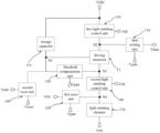
- the pixel driving circuit includes:
- one terminal of the light emitting element 170 is used to load the second power supply voltage VSS, and the other terminal is reset by the second power supply voltage VSS.
- the pixel driving circuit avoids the situation of using the initialization voltage to reset the light-emitting element 170 , reduces the difference in the source-drain voltage difference of the driving crystal points at different positions, improves the uniformity of the operating environment of the driving transistor T 3 , thereby improving the brightness uniformity of the display panel.
- the pixel driving circuit provided by the present disclosure can be applied to a display panel, and the display panel can include a display area D and a peripheral area C surrounding the display area D.
- the pixel driving circuit can be arranged in the display area D, especially arranged in an array in the display area D; the light emitting element 170 of the pixel driving circuit can be used as a sub-pixel of the display panel.
- a binding area E may be provided in the peripheral area C, and the binding area E is used for binding a circuit board or a driver chip.
- the display panel can be bound with a driving chip through a COP (chip on panel) technology.
- the binding area E may include a chip binding area and a circuit board binding area, the chip binding area is provided with a chip binding pad for binding with the driver chip, and the circuit board binding area is provided with a circuit board binding pad for binding with the circuit board.
- the display panel may also be bound with a driving chip through a COF (chip on film) technology.
- the binding area E includes a circuit board binding area, and a circuit board binding pad for binding with the COF is arranged in the circuit board binding area, and a driver chip can be bound to the COF.
- the display panel can also be bound to the driving chip by other methods, for example, the display panel is bound to a flexible circuit board and the driving chip is bound to the flexible circuit board, which is not limited in the present disclosure.
- the light emitting element 170 of the present disclosure may be an organic electroluminescence diode (OLED).
- OLED organic electroluminescence diode
- the display panel may include a base substrate F 100 , a circuit layer F 200 and a pixel layer F 300 which are stacked in sequence.
- the base substrate F 100 may be a base substrate F 100 of inorganic material, or may be a base substrate F 100 of organic material.
- the material of the base substrate F 100 can be glass materials such as soda-lime glass, quartz glass, sapphire glass, or can be metallic material such as stainless steel, aluminum, nickel, etc.
- the material of the substrate F 100 may be Polymethyl methacrylate (PMMA), Polyvinyl alcohol (PVA), Polyvinyl phenol (PVP), Polyether sulfone (PES), polyimide, polyamide, polyacetal, Polycarbonate (PC), Polyethylene terephthalate (PET), Polyethylene naphthalate (PEN) or a combination thereof.
- the base substrate F 100 may also be a flexible base substrate F 100 , for example, the material of the base substrate F 100 may be polyimide (PI).
- the base substrate F 100 can also be a composite of multi-layer materials.
- the base substrate F 100 can include a bottom film, a pressure-sensitive adhesive layer, a first polyimide layer and a second polyimide layer.
- each power supply in the pixel driving circuit may include a transistor F 200 M and a storage capacitor.
- the transistor F 200 M can be a thin film transistor, and the thin film transistor can be a top gate thin film transistor, a bottom gate thin film transistor or a double gate thin film transistor;
- the material of the active layer of the thin film transistor can be amorphous silicon semiconductor material, low temperature polysilicon semiconductor materials, metal oxide semiconductor materials, organic semiconductor materials or other types of semiconductor materials;
- the thin film transistors may be N-type thin film transistors or P-type thin film transistors.
- the thin film transistor is a low temperature polysilicon transistor.
- the types of any two transistors may be the same or different.
- some transistors may be N-type transistors and some transistors may be P-type transistors.
- the material of the active layer of some transistors may be low-temperature polysilicon semiconductor material, and the material of the active layer of some transistors may be metal oxide semiconductor materials.
- the transistor may have a first terminal, a second terminal and a control terminal, one of the first and second terminals may be the source of the transistor and the other may be the drain of the transistor, and the control terminal may be the gate of the transistor. It can be understood that the source and the drain of the transistor are two opposite concepts that can be interchanged; when the working state of the transistor changes, for example, the direction of the current changes, the source and the drain of the transistor can be interchanged.
- the circuit layer F 200 may include a semiconductor layer F 203 , a gate insulating layer F 204 , a gate layer F 205 , an interlayer dielectric layer F 206 , and a source-drain metal layer F 207 stacked between the base substrate F 100 and the pixel layer F 300 .
- Each thin film transistor and storage capacitor can be formed of film layers such as semiconductor layer F 203 , gate insulating layer F 204 , gate layer F 205 , interlayer dielectric layer F 206 , and source-drain metal layer F 207 .
- the positional relationship of each film layer can be determined according to the film layer structure of the thin film transistor.
- the circuit layer F 200 may include a semiconductor layer F 203 , a gate insulating layer F 204 , a gate layer F 205 , an interlayer dielectric layer F 206 , and a source-drain metal layer F 207 , which are sequentially stacked.
- the thin film transistor thus formed is a top-gate thin film transistor.
- the circuit layer F 200 may include a gate layer F 205 , a gate insulating layer F 204 , a semiconductor layer F 203 , an interlayer dielectric layer F 206 , and a source-drain metal layer F 207 stacked in sequence, and the thin film transistor thus formed is a bottom gate thin film transistor.
- the circuit layer F 200 can also adopt a double gate layer F 205 structure, that is, the gate layer F 205 can include a first gate layer and a second gate layer, and the gate insulating layer F 204 can include a first gate insulating layer for isolating the semiconductor layer F 203 and the first gate layer, and a second gate insulating layer for isolating the first gate layer and the second gate layer.
- the circuit layer F 200 may include a semiconductor layer F 203 , a first gate insulating layer, a first gate layer, a second gate insulating layer, a second gate layer, an interlayer dielectric layer F 206 and a source-drain metal layer F 207 .
- the circuit layer F 200 can also adopt a structure of a double source-drain metal layer F 207 , that is, the source-drain metal layer F 207 can include a first source-drain metal layer and a second source-drain metal layer, and the interlayer dielectric layer F 206 can include a first interlayer dielectric layer located on the side of the first source-drain metal layer close to the substrate F 100 and a second interlayer dielectric layer located between the first source-drain metal layer and the second source-drain metal layer.
- the circuit layer F 200 may further include a passivation layer, and the passivation layer may be disposed on the surface of the source-drain metal layer F 207 away from the base substrate F 100 to protect the source-drain metal layer F 207 .
- the circuit layer F 200 may also include a buffer material layer disposed between the base substrate F 100 and the semiconductor layer F 203 , and the semiconductor layer F 203 , the gate layer F 205 , etc. are located on the side of the buffer material layer away from the base substrate F 100 .
- the material of the buffer material layer may be inorganic insulating materials such as silicon oxide and silicon nitride.
- the buffer material layer can be one layer of inorganic material, or an inorganic material layer stacked in multiple layers. Exemplarily, in one embodiment of the present disclosure, referring to FIG.
- the buffer material layer may include a barrier layer F 201 on the side close to the base substrate F 100 and a buffer layer F 202 on the side of the barrier layer F 201 away from the base substrate F 100 .
- the barrier layer F 201 is used to prevent the ions and other components in the substrate F 100 from penetrating into the circuit layer F 200 , so that the circuit layer F 200 maintains stable performance.
- the buffer layer F 202 can improve the bonding force between the circuit layer F 200 and the base substrate F 100 , and provide a stable environment for the circuit layer F 200 .
- the circuit layer F 200 may also include a planarization layer F 208 located between the source-drain metal layer F 207 and the pixel layer F 300 .
- the planarization layer F 208 may provide a planarized surface for the pixel electrode.
- the material of the planarization layer F 208 may be an organic material.
- the pixel layer F 300 may be disposed on the side of the circuit layer F 200 away from the base substrate F 100 , and the light emitting element of the pixel driving circuit of the present disclosure may be disposed at the pixel layer F 300 .
- the pixel layer F 300 may include a pixel electrode layer F 301 , a pixel definition layer F 302 , a support pillar layer F 303 , an organic light-emitting functional layer F 304 and a common electrode layer F 305 which are stacked in sequence.
- the pixel electrode layer F 301 has a plurality of pixel electrodes in the display area of the display panel; the pixel definition layer F 302 has a plurality of penetrated pixel openings corresponding to the plurality of pixel electrodes in the display area, and any pixel opening exposes at least a partial area of the corresponding pixel electrode.
- the support pillar layer F 303 includes a plurality of support pillars in the display area, and the support pillars are located on the surface of the pixel definition layer F 302 away from the base substrate F 100 , so as to support a fine metal mask (FMM) during the evaporation process.
- the organic light emitting functional layer F 304 at least covers the pixel electrodes exposed by the pixel definition layer F 302 .
- the organic light-emitting functional layer F 304 may include an organic electroluminescent material layer, and may include one or more of a hole injection layer, a hole transport layer, an electron blocking layer, a hole blocking layer, an electron transport layer, and an electron injection layer.
- Each film layer of the organic light-emitting functional layer F 304 can be prepared by an evaporation process, and a fine metal mask or an open mask can be used to define the pattern of each film layer during evaporation.
- the common electrode layer F 305 can cover the organic light-emitting functional layer F 304 in the display area.
- the pixel electrode, the common electrode layer F 305 and the organic light-emitting functional layer F 304 between the pixel electrode and the common electrode layer F 305 form an organic light-emitting diode, and any organic light-emitting diode can be used as a sub-pixel of the display panel.
- the pixel layer F 300 may also include a light extraction layer located on the side of the common electrode layer F 305 away from the base substrate F 100 to enhance the light extraction efficiency of the organic light emitting diode.
- the display panel may further include a thin film encapsulation layer F 400 .
- the thin film encapsulation layer F 400 is disposed on the surface of the pixel layer F 300 away from the base substrate F 100 , and may include alternately stacked inorganic encapsulation layers and organic encapsulation layers.
- the inorganic encapsulation layer can effectively block moisture and oxygen from the outside, preventing water and oxygen from invading the organic light-emitting functional layer F 304 and causing material degradation.
- the edge of the inorganic encapsulation layer may be located in the peripheral area.
- the organic encapsulation layer is located between two adjacent inorganic encapsulation layers, so as to realize planarization and weaken the stress between the inorganic encapsulation layers.
- the edge of the organic encapsulation layer may be located between the display area and the edge of the inorganic encapsulation layer.
- the thin film encapsulation layer F 400 includes a first inorganic encapsulation layer F 401 , an organic encapsulation layer F 402 and a second inorganic encapsulation layer F 403 sequentially stacked on the side of the pixel layer F 300 away from the base substrate F 100 .
- the display panel may also include an anti-reflection layer F 500 .
- the anti-reflection layer F 500 may be disposed on a side of the film encapsulation layer F 400 away from the pixel layer F 300 to reduce the reflection of ambient light by the display panel, thereby reducing the impact of ambient light on the display effect.
- the anti-reflection layer F 500 may include a color filter layer and a black matrix layer that are stacked, so that reducing of the light transmittance of the display panel can be avoided while the ambient light interference is reduced.
- the antireflection layer F 500 may be a polarizer, such as a patterned coated circular polarizer.
- the display panel may further include a touch function layer F 600 , which is disposed on a side of the thin film encapsulation layer F 400 away from the base substrate F 100 for realizing touch operation of the display panel.
- the touch function layer F 600 may be disposed between the thin film encapsulation layer F 400 and the antireflection layer F 500 .
- the display panel has a data lead 220 formed on the source and drain metal layer.
- the data lead 220 may extend along the column direction B and be electrically connected to the data writing unit 110 for loading the data voltage Vdata to the data writing unit 110 .
- the display panel is provided with a scan lead 210 on the gate layer.
- the scan lead 210 is extended along the row direction A and is used to load the scan signal Vgate.
- the scan lead 210 may be electrically connected to the data writing unit 110 , the threshold compensation unit 120 and the first reset unit 150 .
- the display panel is provided with an emission control lead 240 on the gate layer, and the emission control lead 240 is extended along the row direction A and is used for loading an emission control signal EM.
- the light emitting control lead 240 can be electrically connected with the first light emitting control unit 130 and the second light emitting control unit 140 .
- the display panel is provided with a first power supply lead 231 on the circuit layer, and the first power supply lead 231 is used to load the first power supply voltage VDD.
- the first power lead 231 may be connected to the first light emitting control unit 130 to load the first power supply voltage VDD to the first light emitting control unit 130 .
- the first power supply lead 231 is arranged in the display area D and distributed in a grid, so that the uniformity of the first power supply voltage VDD on the first power supply leads 231 can be improved.
- the first power lead 231 is disposed at the source-drain metal layer. In another embodiment of the present disclosure, the first power lead 231 may be partially disposed at the source-drain metal layer and partially disposed at the gate layer.
- the first power supply leads 231 are distributed in a grid shape, and the portions extending along the column direction may be disposed at the source and drain metal layers, and the portions extending along the row direction may be disposed at the gate electrode layer.
- the display panel may also be provided with a first power supply bus 232 .
- the first power supply bus 232 is disposed in the peripheral area C, and one end thereof is extended to the bonding area E.
- the first power supply bus 232 can be connected to the bonding pad in the binding area E, and by virtue of the binding connection of the circuit board and the display panel in the bonding area E, the first power supply bus 232 circuitry extended to the circuit board, so as to receive the first power supply voltage VDD from the circuit board.
- the first power supply bus 232 is connected to the first power lead 231 for loading the first power voltage VDD and distributing the first power voltage VDD to each first power lead 231 .
- the number of the first power supply buses 232 may be two, and the two first power supply buses 232 may be symmetrically distributed.
- the first power supply bus 232 is disposed at the source-drain metal layer.
- the display panel may further be provided with a second power supply lead 251 for applying the second power supply voltage VSS, and the second power supply lead 251 is electrically connected to the fourth node N 4 of the pixel driving circuit.
- any second power lead 251 is extended along the row direction A or along the column direction B. Further optionally, any pixel driving circuit area has a second power lead 251 passing through it.
- the second power supply lead 251 includes a plurality of second power supply row sub-leads 2511 extending along the row direction A and a plurality of second power supply column sub-leads 2512 extending along the column direction B; the second power supply row sub-leads 2511 and the second power column sub-leads 2512 are connected to each other, so that the respective second power supply lead 251 is in a grid shape.
- the second power lead 251 is designed in a grid shape, which can improve the uniformity of the second power supply voltage VSS in the display panel, reduce the voltage drop of the second power supply voltage VSS, and further improve the brightness uniformity of the display panel.
- the second power lead 251 may be disposed at the source-drain metal layer, for example, may cross and extend between the first source-drain metal layer and the second source-drain metal layer.
- the second power lead 251 may also be partially disposed at other film layers, for example, may be partially disposed at film layers such as semiconductor layers, gate layers, and pixel electrode layers.
- the peripheral area C is provided with a second power supply bus 252 , and the second power supply bus 252 is connected to at least part of the second power leads 251 .
- the second power supply bus 252 is electrically connected to the binding area E, and can be loaded with the second power supply voltage VSS, and then distribute the second power supply voltage VSS to the second power supply leads 251 . It can be understood that if some of the second power leads 251 are not directly connected to the second power supply bus 252 , they can be electrically connected to the second power supply bus 252 through other conductive structures, such as other second power leads 251 .
- the number of the second power supply bus 252 is two, and they are arranged symmetrically.
- the second power supply bus 252 has a wiring segment 2521 and a connecting segment 2522 connected to each other; the number of the second power supply bus 252 is two, and the wiring segments 2521 of the two second power supply buses 252 extend along the column direction B and are respectively located on two sides of the display area D; the connecting segment 2522 of the second power supply bus 252 is extended to the bonding area E.
- the common electrode of the display panel may cover the display area and extend to the peripheral area, and partially overlap the wiring segment 2521 of the second power supply bus 252 , so that the second power supply bus 252 can apply the second power supply voltage VSS to the common electrode.
- the pixel electrode layer can be provided with an interconnecting electrode, the interconnecting electrode can be connected to the second power supply bus 252 through a via hole, and the common electrode can be connected to the interconnecting electrode, thereby realizing the electrical connection between the common electrode and the second power supply bus 252 .
- the wiring segment 2521 of the second power supply bus 252 is extended along the column direction B; and at least part of the second power lead 251 is extended along the row direction A to connect with the wiring segments 2521 of the two second power buses 252 .
- the second power supply voltage VSS may be loaded to the second power supply lead 251 by the low-impedance second power supply bus 252 , thereby further improving the uniformity of the second power supply voltage VSS.
- the part of the second power lead 251 extending along the row direction A such as the respective second power row sub-lead 2511 , is connected to two wiring segments 2521 of the second power supply bus 252 at both ends.
- the wiring segment 2521 of the second power supply bus 252 is located at an end of the display panel close to the bonding area E.
- the length of the wiring segment 2521 of the second power supply bus 252 is shorter than the length of the display area D in the column direction B, and the wiring segment 2521 of the second power supply bus 252 is only provided on one side close to the bonding area E.
- This arrangement can reduce the extension length of the wiring segment 2521 of the second power supply bus 252 , thereby reducing the frame space occupied by the wiring segment 2521 of the second power supply bus 252 , and further reducing the frame of the display panel.
- the wiring segment 2521 of the second power supply bus 252 may only be located at the corner of the display panel near the binding area E, that is, outside the two corners of the display area D close to the binding area E. In this way, the wiring segment 2521 of the second power supply bus 252 does not extend further along the column direction B, thereby significantly reducing the frame width of the display panel.
- the second power supply leads 251 can be distributed in grid form and electrically connected to the wiring segment 2521 of the second power supply bus 252 to ensure that the second power supply voltage VS S can be applied to the fourth node N 4 of each pixel driving circuit.
- a node refers to a conductive structure that has equipotential and is electrically connected to each other.
- the conductive structure can be the same conductive structure located in the same film layer, can be different conductive structures located in the same film layer, or can be different conductive structures located in different layers.
- the data writing unit 110 includes a data writing transistor T 4 .
- the data writing transistor T 4 has a first terminal, a second terminal and a control terminal. The first terminal of the data writing transistor T 4 is used to load the data voltage Vdata, the second terminal of the data writing transistor T 4 is connected to the second node N 2 , and the control terminal of the data writing transistor T 4 is used to load the scan signal Vgate.
- the first terminal of the data writing transistor T 4 may be electrically connected to the data lead 220 , and the control terminal of the data writing transistor T 4 may be electrically connected to the scan lead 210 .
- control terminal of the transistor is electrically connected to the scan lead 210 , which may mean that the gate of the transistor is multiplexed as a part of the scan lead 210 (that is, the scan lead 210 overlaps with the active layer of the transistor), or may mean that the gate of the transistor is directly or indirectly connected to the scan lead 210 .
- the threshold compensation unit 120 includes a threshold compensation transistor T 2 , the threshold compensation transistor T 2 has a first terminal, a second terminal and a control terminal, and the first terminal of the threshold compensation transistor T 2 is connected to the first node N 1 , the second terminal of the threshold compensation transistor T 2 is connected to the third node N 3 , and the control terminal of the threshold compensation transistor T 2 is used to load the scan signal Vgate.
- control terminal of the threshold compensation transistor T 2 is electrically connected to the scan lead 210 .
- the first light emitting control unit 130 includes a first light emitting control transistor T 5 , and the first light emitting control transistor T 5 has a first terminal, a second terminal and a control terminal.
- the first terminal of the first light emitting control transistor T 5 is used to load the first power supply voltage VDD
- the second terminal of the first light emitting control transistor T 5 is connected to the second node N 2
- the control terminal of the first light emitting control transistor T 5 is used to load the light emitting control signal EM.
- the first terminal of the first light emitting control transistor T 5 is electrically connected to the first power lead 231
- the control terminal of the first light emitting control transistor T 5 is electrically connected to the light emitting control lead 240 .
- control terminal of the transistor is electrically connected to the light emitting control lead 240 , which may mean that the gate of the transistor is multiplexed as a part of the light emitting control lead 240 (that is, the light emitting control lead 240 overlaps with the active layer of the transistor), or may mean that the gate of the transistor is directly or indirectly connected to the light emitting control lead 240 .
- the second light emitting control unit 140 includes a second light emitting control transistor T 6 , the second light emitting control transistor T 6 has a first terminal, a second terminal and a control terminal, and the first terminal of the second light emitting control transistor T 6 is connected to the third node N 3 , the second terminal of the second light emitting control transistor T 6 is connected to the fourth node N 4 , and the control terminal of the second light emitting control transistor T 6 is used to load the light emitting control signal EM.
- the second terminal of the second light emitting control transistor T 6 is connected to the pixel electrode, and the pixel electrode may be part of the fourth node N 4 of the present disclosure; and the control terminal of the second light emitting control transistor T 6 is electrically connected to the light emitting control lead 240 .
- the first reset unit 150 includes a first reset transistor T 7 .
- the first reset transistor T 7 has a first terminal, a second terminal and a control terminal. The first terminal of the first reset transistor T 7 is used to load the second power supply voltage VSS, the second terminal of the first reset transistor T 7 is connected to the fourth node N 4 , and the control terminal of the first reset transistor T 7 is used to load the scan signal Vgate.
- the first terminal of the first reset transistor T 7 is electrically connected to the second power lead 251
- the second terminal of the first reset transistor T 7 is electrically connected to the pixel electrode
- the control terminal of the first reset transistor T 7 is electrically connected to the scan lead 210 .
- one terminal of the storage capacitor Cst is electrically connected to the first node N 1 , and the other terminal can be used for loading the first power supply voltage VDD, and can also be used for loading the second power supply voltage VS S.
- the pixel driving circuit further includes a second reset unit 160 connected to the first node N 1 for applying an initialization voltage Vinit to the first node N 1 in response to the reset control signal Vreset.
- the pixel driving circuit can also reset the first node N 1 to improve the stability and uniformity of the operation of each display driving circuit.
- the second reset unit 160 may include a second reset transistor T 1 , and the second reset transistor T 1 has a first terminal, a second terminal and a control terminal, wherein the first terminal of the second reset transistor T 1 is used to load the initialization voltage Vinit, the second terminal of the second reset transistor T 1 is electrically connected to the first node N 1 , and the control terminal of the second reset transistor T 1 is used to load the reset control signal Vreset.
- the display panel may be provided with a reset control lead 270 for loading the reset control signal Vreset.
- the reset control lead 270 may extend along the row direction A and be electrically connected to the gate of the second reset transistor T 1 .
- the reset control lead 270 may be disposed at the gate layer.
- the display panel may be provided with an initialization lead 261 , which is used to load the initialization voltage Vinit.
- the initialization lead 261 may extend along the row direction A and be electrically connected to the first terminal of the second reset transistor T 1 .
- the initialization lead 261 may run through the display area D along the row direction A.
- the initialization lead 261 may be provided at the source-drain metal layer.
- the display panel can also be provided with an initialization bus 262 , and the initialization bus 262 is used to load the initialization voltage Vinit; the number of the initialization bus 262 is two, and the initialization bus 262 is located in the peripheral area C, and the initialization bus 262 includes interconnected wiring segment 2621 and connecting segment 2622 ; the wiring segments 2621 of the two initialization buses 262 is extended along the column direction B and are respectively located on both sides of the display area D; the connecting segment 2622 of the initialization bus 262 is extended to the binding region E.
- the initialization lead 261 runs through the display area D along the row direction A and is connected to the wiring segment 2621 of the initialization bus 262 .
- the initialization bus 262 can distribute the initialization voltage Vinit to each initialization lead 261 and improve the uniformity of the initialization voltage Vinit.
- the initialization bus 262 is located between the second power supply bus 252 and the display area D.
- the connecting segment 2622 of the two initialization buses 262 is located at the inner side of the two first power supply buses 232 .
- the connecting segments 2622 of the two initialization buses 262 are bent to both sides of the row direction A of the display panel, which makes the connecting segments 2622 of the two initialization buses 262 partially overlap with the first power supply bus 232 .
- the scan lead 210 within the range of a pixel driving circuit, along the column direction, the scan lead 210 , the first power supply lead 231 , the light emitting control lead 240 , the initialization lead 261 and the reset control lead 270 are arranged sequentially.
- the display panel is provided with a through hole F in the display area D.
- the pixel driving circuit of the present disclosure uses the second power supply voltage VSS to initialize the fourth node N 4 of the pixel driving circuit; compared with the conventional initialization voltage Vinit, the distribution of the second power supply voltage VSS is more uniform and the voltage drop is smaller, which is less affected by the magnitude of the load (the number of light emitting elements 170 ).
- Implementations of the present disclosure further provide a display device, which includes any display panel described in the above display panel embodiments.
- the display device may be a smart watch screen, a smart phone screen or other types of display devices. Since the display device has any one of the display panels described in the above display panel implementation manners, it has the same beneficial effect, which will not be repeated here in the present disclosure.
Landscapes
- Engineering & Computer Science (AREA)
- Physics & Mathematics (AREA)
- Computer Hardware Design (AREA)
- General Physics & Mathematics (AREA)
- Theoretical Computer Science (AREA)
- Microelectronics & Electronic Packaging (AREA)
- Electroluminescent Light Sources (AREA)
- Control Of Indicators Other Than Cathode Ray Tubes (AREA)
Abstract
Description
-
- a driving transistor connected to a first node, a second node and a third node, and configured to output a driving current to the third node under control of the first node;
- a storage capacitor, including one terminal connected to the first node;
- a data writing unit, connected to the second node, and configured to load a data voltage to the second node in response to a scan signal;
- a threshold compensation unit, connected to the first node and the third node, and configured to conduct the first node and the third node in response to the scan signal;
- a first light emitting control unit, connected to the second node, and configured to apply a first power supply voltage to the second node in response to a light emitting control signal;
- a second light emitting control unit, connected to the third node and a fourth node, and configured to conduct the third node and the fourth node in response to the light emitting control signal;
- a first reset unit, connected to the fourth node, and configured to apply a second power supply voltage to the fourth node in response to the scan signal; and
- a light emitting element, one terminal of the light emitting element is connected to the fourth node, and the other terminal is configured to load the second power supply voltage.
-
- the threshold compensation unit includes a threshold compensation transistor, the threshold compensation transistor has a first terminal, a second terminal and a control terminal, the first terminal of the threshold compensation transistor is connected to the first node, the second terminal of the threshold compensation transistor is connected to the third node, and the control terminal of the threshold compensation transistor is configured to load the scan signal;
- the first light emitting control unit includes a first light emitting control transistor, the first light emitting control transistor has a first terminal, a second terminal and a control terminal, and the first terminal of the first light emitting control transistor is configured to load the first power supply voltage, the second terminal of the first light emitting control transistor is connected to the second node, and the control terminal of the first light emitting control transistor is configured to load the light emitting control signal;
- the second light emitting control unit includes a second light emitting control transistor, the second light emitting control transistor has a first terminal, a second terminal and a control terminal, and the first terminal of the second light emitting control transistor is connected to the third node, the second terminal of the second light emitting control transistor is connected to the fourth node, and the control terminal of the second light emitting control transistor is configured to load the light emitting control signal; and
- the first reset unit includes a first reset transistor, the first reset transistor has a first terminal, a second terminal and a control terminal, the first terminal of the first reset transistor is configured to load the second power supply voltage, the second terminal of the first reset transistor is connected to the fourth node, and the control terminal of the first reset transistor is configured to load the scan signal.
-
- an initialization bus, configured to load the initialization voltage; a number of the initialization bus is two and are disposed in the peripheral area, and the initialization bus includes a wiring segment and a connecting segment connected to each other; the wiring segments of the two initialization buses are all extend along the column direction and are respectively located on two sides of the display area; and the connecting segment of the initialization bus extends to the bonding area;
- an initialization lead, running through the display area along a row direction and connected to the wiring segment of the initialization bus;
- a first power supply bus, configured to load the first power supply voltage; a number of the first power supply buses is two and are disposed in the peripheral area, one terminal of the first power supply bus is extended to the bonding area; and
- a first power lead, arranged in the display area and distributed in a grid, and connected to the first power supply bus;
- wherein the first power supply bus is partially overlapped with the initialization bus.
-
- a driving transistor T3, connected to a first node N1, a second node N2 and a third node N3, and is configured to output a driving current to the third node N3 under the control of the first node N1;
- a storage capacitor Cst, having one terminal connected to the first node N1;
- a
data writing unit 110, connected to the second node N2, and is configured to load a data voltage Vdata to the second node N2 in response to a scan signal Vgate; - a
threshold compensation unit 120, connected to the first node N1 and the third node N3, and is configured to cause conduction between the first node N1 and the third node N3 in response to the scan signal Vgate; - a first light emitting
control unit 130, connected to the second node N2, and is configured to load a first power supply voltage VDD to the second node N2 in response to a light emitting control signal EM; - a second light emitting
control unit 140, connected to the third node N3 and the fourth node N4, and is configured to conduct between the third node N3 and the fourth node N4 in response to the light emitting control signal EM; - a
first reset unit 150, connected to a fourth node N4, and is configured to load a second power supply voltage VSS to the fourth node N4 in response to the scan signal Vgate; and - a
light emitting element 170, having one terminal connected to the fourth node N4, and the other configured to load the second power supply voltage VSS.
Claims (18)
Applications Claiming Priority (3)
| Application Number | Priority Date | Filing Date | Title |
|---|---|---|---|
| CN202110322033.8 | 2021-03-25 | ||
| CN202110322033.8A CN113066435B (en) | 2021-03-25 | 2021-03-25 | Pixel driving circuit, display panel and display device |
| PCT/CN2021/132462 WO2022199084A1 (en) | 2021-03-25 | 2021-11-23 | Pixel drive circuit, display panel and display device |
Publications (2)
| Publication Number | Publication Date |
|---|---|
| US20240161699A1 US20240161699A1 (en) | 2024-05-16 |
| US12223909B2 true US12223909B2 (en) | 2025-02-11 |
Family
ID=76563551
Family Applications (1)
| Application Number | Title | Priority Date | Filing Date |
|---|---|---|---|
| US18/282,242 Active US12223909B2 (en) | 2021-03-25 | 2021-11-23 | Pixel drive circuit, display panel and display device |
Country Status (3)
| Country | Link |
|---|---|
| US (1) | US12223909B2 (en) |
| CN (1) | CN113066435B (en) |
| WO (1) | WO2022199084A1 (en) |
Families Citing this family (8)
| Publication number | Priority date | Publication date | Assignee | Title |
|---|---|---|---|---|
| CN113066435B (en) | 2021-03-25 | 2022-07-12 | 京东方科技集团股份有限公司 | Pixel driving circuit, display panel and display device |
| CN116547738A (en) * | 2021-09-18 | 2023-08-04 | 京东方科技集团股份有限公司 | Pixel circuit, driving method and display device |
| CN114255671B (en) * | 2021-12-17 | 2024-10-01 | 重庆惠科金渝光电科技有限公司 | Micro light emitting diode display panel and display device |
| DE112021008527T5 (en) * | 2021-12-21 | 2024-10-24 | Boe Technology Group Co., Ltd. | shift register, scan driver circuit and display substrate |
| US20240292657A1 (en) * | 2022-05-31 | 2024-08-29 | Chengdu Boe Optoelectronics Technology Co., Ltd. | Display substrate and display device |
| WO2024243810A1 (en) * | 2023-05-30 | 2024-12-05 | 京东方科技集团股份有限公司 | Display substrate and display apparatus |
| CN118015990B (en) * | 2024-03-22 | 2025-09-26 | 成都京东方光电科技有限公司 | Display panel and display device |
| CN119580637A (en) * | 2024-10-21 | 2025-03-07 | 京东方科技集团股份有限公司 | Display panel and manufacturing method, and display device |
Citations (13)
| Publication number | Priority date | Publication date | Assignee | Title |
|---|---|---|---|---|
| US20030103022A1 (en) | 2001-11-09 | 2003-06-05 | Yukihiro Noguchi | Display apparatus with function for initializing luminance data of optical element |
| US20040257353A1 (en) * | 2003-05-19 | 2004-12-23 | Seiko Epson Corporation | Electro-optical device and driving device thereof |
| US20050057461A1 (en) * | 2003-08-28 | 2005-03-17 | Mi-Sook Suh | Flat panel display device with compensated voltage drop |
| US20130241916A1 (en) * | 2010-05-18 | 2013-09-19 | Lg Display Co., Ltd. | Voltage compensation type pixel circuit of active matrix organic light emitting diode display device |
| US20140145917A1 (en) | 2012-11-27 | 2014-05-29 | Lg Display Co., Ltd. | Organic light emitting diode display device and method of driving the same |
| CN107103882A (en) | 2017-06-29 | 2017-08-29 | 京东方科技集团股份有限公司 | A kind of image element circuit, its driving method and display panel |
| US20170365214A1 (en) | 2016-06-15 | 2017-12-21 | Apple Inc. | Light-Emitting Diode Display With Reduced Leakage |
| US20180144684A1 (en) | 2016-11-18 | 2018-05-24 | Samsung Display Co., Ltd. | Organic light emitting diode display |
| US20190066598A1 (en) | 2017-08-31 | 2019-02-28 | Lg Display Co., Ltd. | Electroluminescent display device and driving method thereof |
| CN109599062A (en) | 2017-09-30 | 2019-04-09 | 京东方科技集团股份有限公司 | Pixel circuit and its driving method, display device |
| US20190266941A1 (en) * | 2018-02-28 | 2019-08-29 | Samsung Display Co, Ltd. | Display device and method of driving the same |
| US20200394950A1 (en) | 2019-06-12 | 2020-12-17 | Samsung Display Co., Ltd. | Display device |
| CN113066435A (en) | 2021-03-25 | 2021-07-02 | 京东方科技集团股份有限公司 | Pixel driving circuit, display panel and display device |
-
2021
- 2021-03-25 CN CN202110322033.8A patent/CN113066435B/en active Active
- 2021-11-23 US US18/282,242 patent/US12223909B2/en active Active
- 2021-11-23 WO PCT/CN2021/132462 patent/WO2022199084A1/en not_active Ceased
Patent Citations (19)
| Publication number | Priority date | Publication date | Assignee | Title |
|---|---|---|---|---|
| US20030103022A1 (en) | 2001-11-09 | 2003-06-05 | Yukihiro Noguchi | Display apparatus with function for initializing luminance data of optical element |
| US20040257353A1 (en) * | 2003-05-19 | 2004-12-23 | Seiko Epson Corporation | Electro-optical device and driving device thereof |
| US20050057461A1 (en) * | 2003-08-28 | 2005-03-17 | Mi-Sook Suh | Flat panel display device with compensated voltage drop |
| CN1599531A (en) | 2003-08-28 | 2005-03-23 | 三星Sdi株式会社 | Flat panel display device with compensated voltage drop |
| US7893625B2 (en) | 2003-08-28 | 2011-02-22 | Samsung Mobile Display Co., Ltd. | Flat panel display device with compensated voltage drop |
| US20130241916A1 (en) * | 2010-05-18 | 2013-09-19 | Lg Display Co., Ltd. | Voltage compensation type pixel circuit of active matrix organic light emitting diode display device |
| US20140145917A1 (en) | 2012-11-27 | 2014-05-29 | Lg Display Co., Ltd. | Organic light emitting diode display device and method of driving the same |
| US20170365214A1 (en) | 2016-06-15 | 2017-12-21 | Apple Inc. | Light-Emitting Diode Display With Reduced Leakage |
| US10431154B2 (en) | 2016-06-15 | 2019-10-01 | Apple Inc. | Light-emitting diode display with reduced leakage |
| US20180144684A1 (en) | 2016-11-18 | 2018-05-24 | Samsung Display Co., Ltd. | Organic light emitting diode display |
| CN107103882A (en) | 2017-06-29 | 2017-08-29 | 京东方科技集团股份有限公司 | A kind of image element circuit, its driving method and display panel |
| US20200320934A1 (en) | 2017-06-29 | 2020-10-08 | Boe Technology Group Co., Ltd. | Pixel circuit, driving method thereof and display panel |
| US10957257B2 (en) | 2017-06-29 | 2021-03-23 | Boe Technology Group Co., Ltd. | Pixel circuit, driving method thereof and display panel |
| US20190066598A1 (en) | 2017-08-31 | 2019-02-28 | Lg Display Co., Ltd. | Electroluminescent display device and driving method thereof |
| CN109599062A (en) | 2017-09-30 | 2019-04-09 | 京东方科技集团股份有限公司 | Pixel circuit and its driving method, display device |
| US20190266941A1 (en) * | 2018-02-28 | 2019-08-29 | Samsung Display Co, Ltd. | Display device and method of driving the same |
| US10810934B2 (en) | 2018-02-28 | 2020-10-20 | Samsung Display Co., Ltd. | Display device and method of driving the same |
| US20200394950A1 (en) | 2019-06-12 | 2020-12-17 | Samsung Display Co., Ltd. | Display device |
| CN113066435A (en) | 2021-03-25 | 2021-07-02 | 京东方科技集团股份有限公司 | Pixel driving circuit, display panel and display device |
Non-Patent Citations (2)
| Title |
|---|
| International Search Report and Written Opinion mailed on Feb. 11, 2022, in corresponding PCT/CN2021/132462, 8 pages. |
| Office Action issued on Nov. 26, 2021, in corresponding Chinese patent Application No. 202110322033.8, 22 pages. |
Also Published As
| Publication number | Publication date |
|---|---|
| CN113066435B (en) | 2022-07-12 |
| WO2022199084A1 (en) | 2022-09-29 |
| CN113066435A (en) | 2021-07-02 |
| US20240161699A1 (en) | 2024-05-16 |
Similar Documents
| Publication | Publication Date | Title |
|---|---|---|
| US12223909B2 (en) | Pixel drive circuit, display panel and display device | |
| US12347385B2 (en) | Display substrate and display device | |
| US12230182B2 (en) | Pixel circuit and driving method therefor, display substrate, and display apparatus | |
| US12193292B2 (en) | Display substrate and display apparatus | |
| US12266307B2 (en) | Display substrate and display device | |
| US11790847B2 (en) | Display substrate and display device | |
| CN113299229B (en) | Display panel and display device | |
| US11404009B2 (en) | Array substrate and display device | |
| US11910665B2 (en) | Array substrate and display device | |
| US11515383B2 (en) | Display device | |
| US12283581B2 (en) | Display device | |
| US11937470B2 (en) | Array substrate and display device | |
| US11972727B2 (en) | Display substrate and display device | |
| US12484380B2 (en) | Display panel | |
| US20250078759A1 (en) | Display substrate and display device | |
| US20240074266A1 (en) | Display panel and display device | |
| WO2023122880A1 (en) | Display panel and display device | |
| CN115867083B (en) | Display panel and its manufacturing method, display device | |
| US20260020449A1 (en) | Display panel and electronic device comprising the same | |
| CN120379340A (en) | Display panel | |
| KR20250034233A (en) | Display device | |
| CN117438435A (en) | Display panels and display devices |
Legal Events
| Date | Code | Title | Description |
|---|---|---|---|
| AS | Assignment |
Owner name: BOE TECHNOLOGY GROUP CO., LTD., CHINA Free format text: ASSIGNMENT OF ASSIGNORS INTEREST;ASSIGNORS:LIU, TINGLIANG;YANG, HUIJUAN;HAN, LINHONG;AND OTHERS;REEL/FRAME:064914/0691 Effective date: 20230530 Owner name: CHENGDU BOE OPTOELECTRONICS TECHNOLOGY CO., LTD., CHINA Free format text: ASSIGNMENT OF ASSIGNORS INTEREST;ASSIGNORS:LIU, TINGLIANG;YANG, HUIJUAN;HAN, LINHONG;AND OTHERS;REEL/FRAME:064914/0691 Effective date: 20230530 |
|
| FEPP | Fee payment procedure |
Free format text: ENTITY STATUS SET TO UNDISCOUNTED (ORIGINAL EVENT CODE: BIG.); ENTITY STATUS OF PATENT OWNER: LARGE ENTITY |
|
| STPP | Information on status: patent application and granting procedure in general |
Free format text: DOCKETED NEW CASE - READY FOR EXAMINATION |
|
| STPP | Information on status: patent application and granting procedure in general |
Free format text: NON FINAL ACTION MAILED |
|
| STPP | Information on status: patent application and granting procedure in general |
Free format text: RESPONSE TO NON-FINAL OFFICE ACTION ENTERED AND FORWARDED TO EXAMINER |
|
| STPP | Information on status: patent application and granting procedure in general |
Free format text: NOTICE OF ALLOWANCE MAILED -- APPLICATION RECEIVED IN OFFICE OF PUBLICATIONS |
|
| ZAAB | Notice of allowance mailed |
Free format text: ORIGINAL CODE: MN/=. |
|
| STPP | Information on status: patent application and granting procedure in general |
Free format text: AWAITING TC RESP., ISSUE FEE NOT PAID |
|
| STPP | Information on status: patent application and granting procedure in general |
Free format text: NOTICE OF ALLOWANCE MAILED -- APPLICATION RECEIVED IN OFFICE OF PUBLICATIONS |
|
| STPP | Information on status: patent application and granting procedure in general |
Free format text: PUBLICATIONS -- ISSUE FEE PAYMENT RECEIVED |
|
| STPP | Information on status: patent application and granting procedure in general |
Free format text: PUBLICATIONS -- ISSUE FEE PAYMENT VERIFIED |
|
| STCF | Information on status: patent grant |
Free format text: PATENTED CASE |