US12211406B2 - Display panel having crack detection circuit with conduction loop, display apparatus, and method of detecting crack in display panel - Google Patents
Display panel having crack detection circuit with conduction loop, display apparatus, and method of detecting crack in display panel Download PDFInfo
- Publication number
- US12211406B2 US12211406B2 US17/606,432 US202117606432A US12211406B2 US 12211406 B2 US12211406 B2 US 12211406B2 US 202117606432 A US202117606432 A US 202117606432A US 12211406 B2 US12211406 B2 US 12211406B2
- Authority
- US
- United States
- Prior art keywords
- area
- sub
- touch
- crack detection
- line
- Prior art date
- Legal status (The legal status is an assumption and is not a legal conclusion. Google has not performed a legal analysis and makes no representation as to the accuracy of the status listed.)
- Active
Links
Images


Classifications
-
- G—PHYSICS
- G09—EDUCATION; CRYPTOGRAPHY; DISPLAY; ADVERTISING; SEALS
- G09G—ARRANGEMENTS OR CIRCUITS FOR CONTROL OF INDICATING DEVICES USING STATIC MEANS TO PRESENT VARIABLE INFORMATION
- G09G3/00—Control arrangements or circuits, of interest only in connection with visual indicators other than cathode-ray tubes
- G09G3/006—Electronic inspection or testing of displays and display drivers, e.g. of LED or LCD displays
-
- G—PHYSICS
- G01—MEASURING; TESTING
- G01M—TESTING STATIC OR DYNAMIC BALANCE OF MACHINES OR STRUCTURES; TESTING OF STRUCTURES OR APPARATUS, NOT OTHERWISE PROVIDED FOR
- G01M5/00—Investigating the elasticity of structures, e.g. deflection of bridges or air-craft wings
- G01M5/0033—Investigating the elasticity of structures, e.g. deflection of bridges or air-craft wings by determining damage, crack or wear
-
- G—PHYSICS
- G01—MEASURING; TESTING
- G01M—TESTING STATIC OR DYNAMIC BALANCE OF MACHINES OR STRUCTURES; TESTING OF STRUCTURES OR APPARATUS, NOT OTHERWISE PROVIDED FOR
- G01M5/00—Investigating the elasticity of structures, e.g. deflection of bridges or air-craft wings
- G01M5/0083—Investigating the elasticity of structures, e.g. deflection of bridges or air-craft wings by measuring variation of impedance, e.g. resistance, capacitance, induction
-
- H—ELECTRICITY
- H10—SEMICONDUCTOR DEVICES; ELECTRIC SOLID-STATE DEVICES NOT OTHERWISE PROVIDED FOR
- H10K—ORGANIC ELECTRIC SOLID-STATE DEVICES
- H10K59/00—Integrated devices, or assemblies of multiple devices, comprising at least one organic light-emitting element covered by group H10K50/00
- H10K59/10—OLED displays
- H10K59/12—Active-matrix OLED [AMOLED] displays
- H10K59/131—Interconnections, e.g. wiring lines or terminals
-
- H—ELECTRICITY
- H10—SEMICONDUCTOR DEVICES; ELECTRIC SOLID-STATE DEVICES NOT OTHERWISE PROVIDED FOR
- H10K—ORGANIC ELECTRIC SOLID-STATE DEVICES
- H10K59/00—Integrated devices, or assemblies of multiple devices, comprising at least one organic light-emitting element covered by group H10K50/00
- H10K59/40—OLEDs integrated with touch screens
-
- G—PHYSICS
- G09—EDUCATION; CRYPTOGRAPHY; DISPLAY; ADVERTISING; SEALS
- G09G—ARRANGEMENTS OR CIRCUITS FOR CONTROL OF INDICATING DEVICES USING STATIC MEANS TO PRESENT VARIABLE INFORMATION
- G09G2300/00—Aspects of the constitution of display devices
- G09G2300/04—Structural and physical details of display devices
- G09G2300/0421—Structural details of the set of electrodes
- G09G2300/0426—Layout of electrodes and connections
-
- G—PHYSICS
- G09—EDUCATION; CRYPTOGRAPHY; DISPLAY; ADVERTISING; SEALS
- G09G—ARRANGEMENTS OR CIRCUITS FOR CONTROL OF INDICATING DEVICES USING STATIC MEANS TO PRESENT VARIABLE INFORMATION
- G09G2330/00—Aspects of power supply; Aspects of display protection and defect management
- G09G2330/12—Test circuits or failure detection circuits included in a display system, as permanent part thereof
Definitions
- the present invention relates to the field of display technology, more particularly, to a display panel, a display apparatus, and a method of detecting crack in a display panel.
- touch panels include one-glass-solution (OGS) touch panels, on-cell touch panels, and in-cell touch panels.
- OGS one-glass-solution
- the on-cell touch panels provide high touch control accuracy.
- the on-cell touch panels can be classified into single-layer-on-cell (SLOC) touch panels and multi-layer-on-cell (MLOC) touch panels.
- SLOC single-layer-on-cell
- MLOC multi-layer-on-cell
- multiple point touch control can be achieved in the MLOC touch panels with superior touch control accuracy and blanking effects.
- the present disclosure provides a display panel, comprising display elements in a display area; a touch electrode layer at least partially in the display area, wherein the display elements and the touch electrode layer are absent in a window region that is at least partially surrounded by the display area; and a crack detection circuit; wherein the crack detection circuit comprising an integrated circuit; and a first conduction loop electrically connected to the integrated circuit wherein the first conduction loop comprises a window region crack detection line substantially surrounding the window region; and at least a portion of the first conduction loop comprises a first metal line in a first layer and a second metal line in a second layer, the first metal line connected to the second metal line through a via extending through a touch insulating layer.
- the window region crack detection line comprises contiguously a first line portion extending clock-wisely around a first section of a periphery of the window region, a second line portion extending counter-clock-wisely around the first section of the periphery of the window region and a second section of the periphery of the window region, and a third line portion extending clock-wisely around the second section of the periphery of the window region.
- the window region crack detection line comprises contiguously a first line portion extending counter-clock-wisely around a first section of a periphery of the window region, a second line portion extending clock-wisely around the first section of the periphery of the window region and a second section of the periphery of the window region, and a third line portion extending counter-clock-wisely around the second section of the periphery of the window region.
- the first conduction loop further comprises a first touch crack detection line and a second touch crack detection line respectively electrically connected to a first terminal and a second terminal of the window region crack detection line; the first touch crack detection line extends from a first sub-area through a second sub-area into a third sub-area of a peripheral area of the display panel; the second touch crack detection line extends from the third sub-area through the second sub-area back into the first sub-area; and the first touch crack detection line and the second touch crack detection line are at least partially in the second layer, the second layer further comprising mesh blocks of the touch electrode layer.
- the first touch crack detection line and the second touch crack detection line are on a same side relative to the display area.
- the first conduction loop further comprises a first connecting mesh block and a second connecting mesh block respectively electrically connected to a first terminal and a second terminal of a window region crack detection line; the first connecting mesh block and the second connecting mesh block respectively extend through a portion of a touch control area of the display panel; and the first connecting mesh block and the second connecting mesh block are in the second layer, the second layer further comprising mesh blocks of the touch electrode layer.
- a contour of at least one of the first connecting mesh block or the second connecting mesh block has an undulating shape or a zig-zag shape; and at least one of the first connecting mesh block or the second connecting mesh block is internal to a mesh block of the touch electrode layer or between adjacent mesh blocks of the touch electrode layer.
- the first conduction loop further comprises a first lead line connecting the first terminal of the window region crack detection line to the first connecting mesh block and a second lead line connecting the second terminal of the window region crack detection line to the second connecting mesh block; the first lead line and the second lead line are in the first layer spaced apart from the second layer by the touch insulating layer; the first lead line connects to the first connecting mesh block through a via extending through the touch insulating layer; and the second lead line connects to the second connecting mesh block through a via extending through the touch insulating layer.
- the display panel further comprises mesh blocks respectively around the window region, conductive plates respectively connected to the mesh blocks, and conductive bridges, wherein a respective conductive plate directly connected to one or more mesh lines of a respective mesh block, and a respective conductive bridge connecting two adjacent conductive plates; wherein the first lead line and the second lead line respectively cross over at least one of a conductive plate or a conductive bridge.
- the first conduction loop further comprises a third lead line connecting the first connecting mesh block to a first touch crack detection line and a fourth lead line connecting the second connecting mesh block to a second touch crack detection line, the first touch crack detection line and the second touch crack detection line being at least partially in the second layer and in a peripheral area of the display panel, the third lead line and the fourth lead line being in the first layer spaced apart from the second layer by the touch insulating layer; the third lead line connects to the first connecting mesh block through a via extending through the touch insulating layer; and the fourth lead line connects to the second connecting mesh block through a via extending through the touch insulating layer.
- the first touch crack detection line, the second touch crack detection line, the window region crack detection line are parts of a first touch crack sub-loop that continuously extends from a first sub-area of a peripheral area into an area substantially surrounding the window region, and then extends from the area substantially surrounding the window region back to the first sub-area.
- the first conduction loop further comprises a first panel crack sub-loop that continuously extends from a first sub-area of a peripheral area into a third sub-area of the peripheral area of the display panel, and then extends from the third sub-area back to the first sub-area; and a first touch crack detection line and a second touch crack detection line respectively electrically connected to a first terminal and a second terminal of a window region crack detection line; wherein a first terminal of the first panel crack sub-loop is connected to the second touch crack detection line; a second terminal of the first panel crack sub-loop is connected to the integrated circuit; the first touch crack detection line and the second touch crack detection line space apart the first panel crack sub-loop and the display area; the first touch crack detection line extends from a first sub-area through a second sub-area into a third sub-area of a peripheral area of the display panel; and the second touch crack detection line extends from the third sub-area through the second sub-area back into the first sub-area.
- the first touch crack detection line and the second touch crack detection line are in the second layer, the second layer further comprising mesh blocks of the touch electrode layer; and the first panel crack sub-loop is in a layer in a thin film transistor array substrate.
- the crack detection circuit further comprises a first connecting line connecting the first touch crack detection line to a source electrode of a switching transistor, a drain electrode of the switching transistor connected to a data line.
- the second terminal of the first panel crack sub-loop is connected to a first pin in the integrated circuit, which is in turn connected to a second pin in a bonding area for bonding a flexible printed circuit.
- the crack detection circuit further comprises a second conduction loop electrically connected to the integrated circuit; the second conduction loop comprises a third touch crack detection line and a fourth touch crack detection line; the first conduction loop and the second conduction loop are spaced apart from each other, at least a portion of the first conduction loop and at least a portion of the second conduction loop are on opposite sides relative to the display area; the third touch crack detection line and the fourth touch crack detection line respectively extend from a first sub-area through a fourth sub-area into a third sub-area of a peripheral area of the display panel; the third touch crack detection line and the fourth touch crack detection line are connected to each other in the third sub-area; and the third touch crack detection line and the fourth touch crack detection line are at least partially in the second layer, the second layer further comprising mesh blocks of the touch electrode layer.
- the second conduction loop further comprises a second panel crack sub-loop that continuously extends from the first sub-area through the fourth sub-area into the third sub-area of a peripheral area of the display panel and back to the first sub-area; wherein a first terminal of the second panel crack sub-loop is connected to the fourth touch crack detection line; a second terminal of the second panel crack sub-loop is connected to the integrated circuit; and the second panel crack sub-loop is in a layer in a thin film transistor array substrate.
- the display panel further comprises a second connecting line connecting the third touch crack detection line to a source electrode of a switching transistor, a drain electrode of the switching transistor connected to a data line.
- the second terminal of the second panel crack sub-loop is connected to a third pin in the integrated circuit, which is in turn connected to a fourth pin in a bonding area for bonding a flexible printed circuit.
- the crack detection circuit further comprises a third conduction loop continuously extending, sequentially, from a first corner region of a first sub-area, to a second sub-area, to a third sub-area, to the second sub-area, to the first sub-area, to a fourth sub-area, to the third sub-area, to the fourth sub-area, and back to a second corner region of the first sub-area;
- the first sub-area, the second sub-area, the third sub-area, and the fourth sub-area are respectively sub-areas of a peripheral area in the display panel;
- a first terminal and a second terminal of the third conduction loop are respectively connected to two bonding pins in a bonding area for bonding a flexible printed circuit; and the first conduction loop and the second conduction loop space apart the third conduction loop from the display area.
- the present disclosure provides a display apparatus, comprising the display panel described herein or fabricated by a method described herein, and a flexible printed circuit connected to the integrated circuit.
- the crack detection circuit further comprises a third conduction loop continuously extending, sequentially, from a first corner region of a first sub-area, to a second sub-area, to a third sub-area, to the second sub-area, to the first sub-area, to a fourth sub-area, to the third sub-area, to the fourth sub-area, and back to a second corner region of the first sub-area; the first sub-area, the second sub-area, the third sub-area, and the fourth sub-area are respectively sub-areas of a peripheral area in the display panel; and a first terminal and a second terminal of the third conduction loop are respectively connected to two bonding pins bonded to the flexible printed circuit.
- the first conduction loop further comprises a first panel crack sub-loop that continuously extends from a first sub-area of a peripheral area into a third sub-area of a peripheral area of the display panel and hack to the first sub-area; a first touch crack detection line and a second touch crack detection line respectively electrically connected to a first terminal and a second terminal of a window region crack detection fine; a first terminal of the first panel crack sub-loop is connected to the second touch crack detection line; a second terminal of the first panel crack sub-loop is connected to a first pin in the integrated circuit, which is in turn connected to a second pin, the second pin bonded to the flexible printed circuit; and the first touch crack detection line and the second touch crack detection line respectively extend from a first sub-area through a second sub-area into a third sub-area of a peripheral area of the display panel.
- the present disclosure provides a method of detecting crack in a display panel comprising display elements in a display area; a touch electrode layer at least partially in the display area, wherein the display elements and the touch electrode layer are absent in a window region that is at least partially surrounded by the display area, the method comprising providing a first conduction loop; electrically connecting a first terminal of the first conduction loop to an integrated circuit; electrically connecting a second terminal of the first conduction loop to a source electrode of a switching transistor; electrically connecting a drain electrode of the switching transistor to a data line; providing, by the integrated circuit, a voltage signal to the first terminal of the first conduction loop while turning on the switching transistor; and determining presence or absence of a crack in is region having the first conduction loop based on light emitting status of light emitting elements connected to the data line; wherein providing the first conduction loop comprises extending a window region crack detection line of the first conduction loop into a region substantially surrounding the window region; and determining presence or absence of the crack comprises determining presence
- providing the first conduction loop further comprises extending a first touch crack detection line of the first conduction loop from a first sub-area through a second sub-area into a third sub-area of a peripheral area of the display panel, extending a second touch crack detection line of the first conduction loop from the third sub-area through the second sub-area into the first sub-area; and determining presence or absence of the crack further comprises determining presence or absence of a crack in a touch control structure in the first sub-area, the second sub-area, and the third sub-area.
- providing the first conduction loop further comprises extending a first panel crack sub-loop of the first conduction loop from a first sub-area of a peripheral area through a second sub-area into a third sub-area of a peripheral area of the display panel and back to the first sub-area; and determining presence or absence of the crack further comprises determining presence or absence of a crack in a thin film transistor array substrate in the first sub-area, the second sub-area, and the third sub-area.
- the method further comprises providing a second conduction loop; electrically connecting a first terminal of the second conduction loop to an integrated circuit; electrically connecting a second terminal of the second conduction loop to a source electrode of a switching transistor; electrically connecting a drain electrode of the switching transistor to a data line; providing, by the integrated circuit, a voltage signal to the first terminal of the second conduction loop while turning on the switching transistor; and determining presence or absence of a crack in a region having the second conduction loop based on light emitting status of light emitting elements connected to the data line; wherein providing the second conduction loop comprises extending a third touch crack detection line of the second conduction loop from a first sub-area through a fourth sub-area into a third sub-area of a peripheral area of the display panel, and extending a second touch crack detection line of the fourth conduction loop from the third sub-area through the fourth sub-area into the first sub-area; and determining presence or absence of the crack further comprises determining presence or absence of a crack in a touch control
- providing the second conduction loop further comprises extending a second panel crack sub-loop of the second conduction loop from a first sub-area of a peripheral area, through a fourth sub-area into a third sub-area of a peripheral area of the display panel and back to the first sub-area; and determining presence or absence of the crack further comprises determining presence or absence of a crack in a thin film transistor array substrate in the first sub-area, the fourth sub-area, and the third sub-area.
- the method further comprises providing a third conduction loop continuously extending, sequentially, from a first corner region of a first sub-area, to a second sub-area, to a third sub-area, to the second sub-area, to the first sub-area, to a fourth sub-area, to the third sub-area, to the fourth sub-area, and back to a second corner region of the first sub-area; wherein the first sub-area, the second sub-area, the third sub-area, and the fourth sub-area are respectively sub-areas of a peripheral area in the display panel; and determining presence or absence of the crack further comprises measuring a resistance of the third conduction loop.
- the method further comprises respectively connecting a first terminal and a second terminal of the third conduction loop to two bonding pins that are bonded to a flexible printed circuit.
- FIG. 1 is a cross sectional view of a display panel in some embodiments according to the present disclosure.
- FIG. 2 is a schematic diagram illustrating the structure of a display panel having a touch control structure in some embodiments according to the present disclosure.
- FIG. 3 A is a schematic diagram illustrating the structure of a touch control structure in some embodiments according to the present disclosure.
- FIG. 3 B is a cross-sectional view along an A-A′ line in FIG. 3 A .
- FIG. 3 C is a cross-sectional view along a B-B′ line in FIG. 3 A .
- FIG. 4 is a diagram illustrating the structure of a display panel in some embodiments according to the present disclosure.
- FIG. 5 A is a diagram illustrating the structure of a first conduction loop in some embodiments according to the present disclosure.
- FIG. 5 B is a schematic diagram illustrating the structure of a window region crack detection line in some embodiments according to the present disclosure.
- FIG. 5 C is a schematic diagram illustrating the structure of a first touch crack sub-loop in some embodiments according to the present disclosure.
- FIG. 5 D is a schematic diagram illustrating the structure of a first panel crack sub-loop in some embodiments according to the present disclosure.
- FIG. 5 E is a diagram illustrating the structure of a second conduction loop in some embodiments according to the present disclosure.
- FIG. 5 F is a schematic diagram illustrating the structure of a second touch crack sub-loop in some embodiments according to the present disclosure.
- FIG. 5 G is a schematic diagram illustrating the structure of a second panel crack sub-loop in some embodiments according to the present disclosure.
- FIG. 5 H is a schematic diagram illustrating the structure of a third conduction loop in some embodiments according to the present disclosure.
- FIG. 5 I is a schematic diagram illustrating the structure of a window region crack detection line in some embodiments according to the present disclosure.
- FIG. 6 is a schematic diagram illustrating a display area and a peripheral area in a display apparatus in some embodiments according to the present disclosure.
- FIG. 7 A is a detailed zoom-in view surrounding a window region of a display panel in some embodiments according to the present disclosure.
- FIG. 7 B is a further zoom-in view around a first connecting mesh block and a second connecting mesh block in some embodiments according to the present disclosure.
- FIG. 7 C is a cross-sectional view along a C-C′ line in FIG. 7 B .
- FIG. 7 D is a cross-sectional view along a D-D′ line in FIG. 7 B .
- FIG. 8 A is diagram illustrating an arrangement of detection lines in a first region R 1 in FIG. 4 .
- FIG. 8 B is a further zoom-in view of a first sub-region SR 1 in FIG. 8 A .
- FIG. 8 C is a further zoom-in view of a second sub-region SR 2 in FIG. 8 A .
- FIG. 9 is diagram illustrating an arrangement of detection lines in a second region R 2 in FIG. 4 .
- FIG. 10 A is diagram illustrating an arrangement of detection lines in a third region R 3 in FIG. 4 .
- FIG. 10 B is a further zoom-in view of a third sub-region SR 3 in FIG. 10 A .
- FIG. 11 is diagram illustrating an arrangement of detection lines in a fourth region R 4 in FIG. 4 .
- FIG. 12 is a diagram illustrating the structure of a display apparatus in some embodiments according to the present disclosure.
- FIG. 13 is a schematic diagram illustrating the structure of a touch control structure in some embodiments according to the present disclosure.
- FIG. 15 is a schematic diagram illustrating a window region in some embodiments according to the present disclosure.
- FIG. 16 B is a cross-sectional view along an E-E′ line in FIG. 16 A .
- FIG. 18 A is a zoom-in view of a second zoom-in region ZR 2 in FIG. 14 .
- FIG. 18 B is a cross-sectional view along an F-F′ line in FIG. 18 A .
- FIG. 19 is a schematic diagram illustrating the structure of a first conductive bridge in some embodiments according to the present disclosure.
- FIG. 20 A is a zoom-in view of a third zoom-in region ZR 3 in FIG. 14 .
- FIG. 20 B is a cross-sectional view along a G-G′ line in FIG. 20 A .
- the present disclosure provides, inter alia, a display panel, a display apparatus, and a method of detecting crack in a display panel that substantially obviate one or more of the problems due to limitations and disadvantages of the related art.
- the present disclosure provides a display panel.
- the display panel includes display elements in a display area; a touch electrode layer at least partially in the display area, wherein the display elements and the touch electrode layer are absent in a window region that is at least partially surrounded by the display area; and a crack detection circuit.
- the crack detection circuit includes an integrated circuit; and a first conduction loop electrically connected to the integrated circuit.
- the first conduction loop includes a window region crack detection line substantially surrounding the window region.
- at least a portion of the first conduction loop comprises a first metal line in a first layer and a second metal line in a second layer, the first metal line connected to the second metal line through a via extending through a touch insulating layer.
- FIG. 1 is a cross sectional view of a display panel in some embodiments according to the present disclosure.
- the display panel in the display area, includes a base substrate BS, a plurality of thin film transistors TFT on the base substrate BS, a passivation layer PVX on a side of the plurality of thin film transistors TFT away from the base substrate BS, a first planarization layer PLN 1 on a side of the passivation layer PVX away from the base substrate BS, a relay electrode RE on a side of the first planarization layer PLN 1 away from the passivation layer PVX, a second planarization layer PLN 2 on a side of the relay electrode RE away from the first planarization layer PLN 1 , a pixel definition layer PDL on a side of the second planarization layer PLN 2 away from the first planarization layer PLN 1 and defining subpixel apertures, an anode AD on a side of the second planarization layer PLN
- FIG. 2 is a schematic diagram illustrating the structure of a display panel haying a touch control structure in some embodiments according to the present disclosure.
- the touch control structure further includes a plurality of first touch signal lines SL 1 respectively connected to the plurality of first mesh electrodes TE 1 , and a plurality of second touch signal lines SL 2 respectively connected to the plurality of second mesh electrodes TE 2 .
- the display panel further includes a touch control driving integrated circuit TIC.
- the plurality of first touch signal lines SL 1 and the plurality of second touch signal lines SL 2 are connected to the touch control driving integrated circuit TIC.
- FIG. 3 A is a schematic diagram illustrating the structure of a touch control structure in a display panel in some embodiments according to the present disclosure.
- the touch control structure in some embodiments includes a plurality of first mesh electrodes TE 1 arranged in a plurality of rows and a plurality of second mesh electrodes TE 2 arranged in a plurality of columns. Adjacent rows of the plurality of rows are isolated from each other. Adjacent columns of the plurality of columns are isolated from each other.
- the touch control structure is a mutual capacitance type touch control structure.
- the plurality of first mesh electrodes TE 1 are a plurality of touch sensing electrodes
- the plurality of second mesh electrodes TE 2 are a plurality of touch scanning electrodes
- the plurality of first mesh electrodes TE 1 are a plurality of touch scanning electrodes
- the plurality of second mesh electrodes TE 2 are a plurality of touch sensing electrodes.
- the respective one of the plurality of first mesh electrodes TE 1 extends along a second direction DR 2 ; and the respective one of the plurality of second mesh electrodes TE 2 extends along a first direction DR 1 .
- the first direction DR 1 and the second direction DR 2 are two non-parallel directions, for example, the first direction DR 1 and the second direction DR 2 cross over each other.
- the first direction DR 1 and the second direction DR 2 are perpendicular to each other.
- the first direction DR 1 and the second direction DR 2 cross over each other at an inclined angle that is not 90 degrees.
- FIG. 3 B is a cross-sectional view along an A-A′ line in FIG. 3 A .
- FIG. 3 C is a cross-sectional view along a B-B′ line in FIG. 3 A .
- the touch control structure includes a plurality of first mesh electrodes TE 1 arranged in a plurality of rows and a plurality of second mesh electrodes TE 2 arranged in a plurality of columns. The plurality of first mesh electrodes TE 1 and the plurality of second mesh electrodes TE 2 are in the second layer SL 2 .
- the touch control structure further includes a plurality of touch electrode bridges EB in the first layer SL 1 ; and vias Vb extending through the touch insulating layer TI.
- the plurality of touch electrode bridges EB respectively extend through the vias Vb to respectively connect adjacent second mesh blocks in a respective column of the plurality of column of the plurality of second mesh electrodes TE 2 .
- the display panel is configured to display an image in at least a portion of the touch control area TCA.
- display elements of the display panel and the touch control structure are absent; in the display area or at least a portion of the touch control area TCA, both display elements of the display panel and the touch control structure are present.
- the term “display area” refers to an area of a display panel where image is actually displayed.
- the display area may include both a subpixel region and an inter-subpixel region.
- a subpixel region refers to a light emission region of a subpixel, such as a region corresponding to a pixel electrode in a liquid crystal display or a region corresponding to a light emissive layer in an organic light emitting diode display panel.
- An inter-subpixel region refers to a region between adjacent subpixel regions, such as a region corresponding to a black matrix in a liquid crystal display or a region corresponding a pixel definition layer in an organic light emitting diode display panel.
- the inter-subpixel region is a region between adjacent subpixel regions in a same pixel.
- the inter-subpixel region is a region between two adjacent subpixel regions from two adjacent pixels.
- the present display panel further includes a crack detection circuit.
- the crack detection circuit according to the present disclosure can not only detect cracks in the display area DA, but also in the window region.
- the crack detection circuit according to the present disclosure can not only detect cracks in the thin film transistor array substrate of the display panel, but also can detect cracks independently occurring in the touch control structure or adjacent layers. The inventors of the present disclosure discover a sophisticated circuit structure that can accurately detect cracks in the display panel with exceptionally high efficiency.
- At least a portion of the first conduction loop includes a first metal line in a first layer and a second metal line in a second layer, the first metal line connected to the second metal line through a via extending through a touch insulating layer.
- FIG. 5 B is a schematic diagram illustrating the structure of a window region crack detection line in some embodiments according to the present disclosure.
- the window region crack detection line WCDL includes contiguously a first line portion LP 1 extending clock-wisely around a first section SC 1 (e.g., a first half) of a periphery of the window region WR, a second line portion LP 2 extending counter-clock-wisely around the first section SC 1 of the periphery of the window region and a second section SC 2 (e.g., a second half) of the periphery of the window region WR, and a third line portion LP 3 extending clock-wisely around the second section SC 2 of the periphery of the window region WR.
- the first conduction loop CLP 1 further includes a first touch crack detection line TCDL 1 and a second touch crack detection line TCDL 2 respectively electrically connected to a first terminal T 1 and a second terminal T 2 of the window region crack detection line WCDL.
- the first touch crack detection lisle TCDL 1 and the second touch crack detection line TCDL 2 are on a same side relative to the display area DA.
- the first touch crack detection line TCDL 1 spaces apart the second touch crack detection line TCDL 2 and the display area DA.
- FIG. 5 I is a schematic diagram illustrating the structure of a window region crack detection line in some embodiments according to the present disclosure.
- the window region crack detection line WCDL includes contiguously a first line portion LP 1 extending counter-clock-wisely around a first section SC 1 (e.g., a first half) of a periphery of the window region WR, a second line portion LP 2 extending clock-wisely around the first section SC 1 of the periphery of the window region and a second section SC 2 (e.g., a second half) of the periphery of the window region WR, and a third line portion LP 3 extending counter-clock-wisely around the second section SC 2 of the periphery of the window region WR.
- FIG. 6 is a schematic diagram illustrating a display area and a peripheral area in a display apparatus in some embodiments according to the present disclosure.
- the display apparatus includes a display area DA and a peripheral area PA.
- the display area DA is substantially the same as the touch control area TCA in FIG. 4
- the peripheral area PA is substantially the same as the peripheral area PA in FIG. 4 .
- the peripheral area PA includes a first sub-area PA 1 on a first side S 1 of the display area DA, a second sub-area PA 2 on a second side S 2 of the display area DA, a third sub-area PA 3 on a third side S 3 of the display area DA, a fourth sub-area PA 4 on a fourth side S 4 of the display area DA.
- the first side S 1 and the third side S 3 are opposite to each other.
- the second side S 2 and the fourth side S 4 are opposite to each other.
- the first sub-area PA 1 is a sub-area where signal lines of the crack detection circuit (e.g., the first conduction loop) are connected to an integrated circuit.
- the first sub-area PA 1 includes a side region SR and one or more corner regions (e.g., a first corner region CR 1 and a second corner region CR 2 ).
- the one or more corner regions are respectively at a corner of the display panel.
- the one or more corner regions respectively connect the side region SR to one or more adjacent sub-areas of the peripheral area PA.
- the first corner region CR 1 connects the side region SR to the second sub-area PA 2
- the second corner region CR 2 connects the side region SR to the fourth sub-area PA 4 .
- the first touch crack detection line TCDL 1 extends from a first sub-area PA 1 , through a second sub-area PA 2 , into a third sub-area PA 3 of a peripheral area PA of the display panel; the first touch crack detection line TCDL 1 and the second touch crack detection line TCDL 2 respectively connect to the window crack detection line WCDL; and the second touch crack detection line TCDL 2 extends from the third sub-area PA 3 , through the second sub-area PA 2 , back into the first sub-area PA 1 .
- the first touch crack detection line TCDL 1 and the second touch crack detection line TCDL 2 are at least partially in a second layer.
- the second layer SL 2 further includes mesh blocks of the touch electrode layer, e.g., mesh blocks of the plurality of first mesh electrodes TE 1 and the plurality of second mesh electrodes TE 2 .
- FIG. 7 A is a detailed zoom-in view surrounding a window region of a display panel in some embodiments according to the present disclosure.
- FIG. 7 B is a further zoom-in view around a first connecting mesh block and a second connecting mesh block in some embodiments according to the present disclosure.
- the first conduction loop further comprises a first connecting mesh block MBC 1 and a second connecting mesh block MBC 2 respectively electrically connected to a first terminal T 1 and a second terminal T 2 of a window region crack detection line WCDL.
- a contour of at least one of the first connecting mesh block MBC 1 and the second connecting mesh block MBC 2 has an undulating shape or a zig-zag shape.
- each of the first connecting mesh block MBC 1 and the second connecting mesh block MBC 2 has an undulating shape or a zig-zag shape.
- at least one of the first connecting mesh block MBC 1 or the second connecting mesh block MBC 2 is internal to a mesh block of the touch electrode layer or between adjacent mesh blocks of the touch electrode layer.
- each of the first connecting mesh block MBC 1 and the second connecting mesh block MBC 2 is internal to a mesh block of the touch electrode layer or between adjacent mesh blocks of the touch electrode layer.
- the first connecting mesh block MBC 1 and the second connecting mesh block MBC 2 are in a second layer.
- the second layer SL 2 further includes mesh blocks of the touch electrode layer, e.g., mesh blocks of the plurality of first mesh electrodes TE 1 and the plurality of second mesh electrodes TE 2 .
- the first connecting mesh block MBC 1 and the second connecting mesh block MBC 2 are in a same layer as the mesh blocks of the plurality of first mesh electrodes TE 1 and the plurality of second mesh electrodes TE 2 .
- the first conduction loop CLP 1 further includes first lead line LL 1 connecting the first terminal T 1 of the window region crack detection line WCDL to the first connecting mesh block MBC 1 and a second lead line LL 2 connecting the second terminal T 2 of the window region crack detection line WCDL to the second connecting mesh block MBC 2 .
- the first lead line and the second lead line are in a first layer spaced apart from the second layer by a touch insulating layer (e.g., the touch insulating layer TI in FIG. 3 B and FIG. 3 C ).
- FIG. 7 C is a cross-sectional view along a C-C′ line in FIG. 7 B .
- the first lead line LL 1 connects to the first connecting mesh block MBC 1 through a via extending through the touch insulating layer TI.
- FIG. 7 D is a cross-sectional view along a D-D′ line in FIG. 7 B . Referring to FIG.
- the second lead line LL 2 connects to the second connecting mesh block MBC 2 through a via extending through the touch insulating layer TI.
- the first lead line LL 1 and the second lead line LL 2 are in a first layer SL 1 spaced apart from the second layer SL 2 by the touch insulating layer TI.
- the second layer SL 2 in some embodiments includes the first line portion LP 1 , the second line portion LP 2 , the third line portion LP 3 , the first connecting mesh block MBC 1 , the second connecting mesh block MBC 2 , at least a sub-layer of a respective touch control signal line of touch control signal lines SGL, the first touch crack detection line TCDL 1 , and the second touch crack detection hue TCDL 2 .
- the display panel in some embodiments further includes mesh blocks MB respectively around the window region WR, conductive plates CP respectively connected to the mesh blocks, and conductive bridges CB, wherein a respective conductive plate is directly connected to one or more mesh lines of a respective mesh block, and a respective conductive bridge connects two adjacent conductive plates.
- the first lead line LL 1 and the second lead line LL 2 respectively cross over at least one of a conductive plate or a conductive bridge. Specifically, the first lead line LL 1 in one example crosses over a conductive bridge, and the second lead line LL 2 in one example crosses over a conductive bridge and a conductive plate.
- the first conduction loop in some embodiments further includes a third lead line LL 3 connecting the first connecting mesh block MBC 1 to a first touch crack detection line TCDL 1 and a fourth lead line LL 4 connecting the second connecting mesh block MBC 2 to a second touch crack detection line TCDL 2 .
- the first touch crack detection line TCDL 1 and the second touch crack detection line TCDL 2 are at least partially in the second layer SL 2 and in a peripheral area of the display panel
- the third lead line LL 3 and the fourth lead line LL 4 are in a first layer SL 1 spaced apart from the second layer SL 2 by the touch insulating layer TI.
- the third lead line LL 3 connects to the first connecting mesh block MBC 1 through a via extending through the touch insulating layer TI.
- the fourth lead line LL 4 connects to the second connecting mesh block MBC 2 through a via extending through the touch insulating layer TI.
- the first conduction loop CLP 1 includes a first metal line in the first layer SL 1 and a second metal line in the second layer SL 2 , the first metal line connected to the second metal line through a via extending through a touch insulating layer TI.
- the first lead line LL 1 , the second lead line LL 2 , the third lead line LL 3 , and the fourth lead line LL 4 are in the first layer SL 1 , e.g., in a same layer as the first metal line.
- at least a portion of the first touch crack detection line TCDL 1 is in the first layer SL 1 , e.g., in a same layer as the first metal line.
- the second touch crack detection line TCDL 2 is in the first layer SL 1 , e.g., in a same layer as the first metal line.
- the first connecting mesh block MBC 1 is in the first layer SL 1 , e.g., in a same layer as the first metal line.
- the second connecting mesh block MBC 2 is in the first layer SL 1 , e.g., in a same layer as the first metal line.
- FIG. 5 C is a schematic diagram illustrating the structure of a first touch crack sub-loop in some embodiments according to the present disclosure.
- the first touch crack detection line TCDL 1 , the second touch crack detection line TCDL 2 , the window region crack detection line WCDL are parts of a first touch crack sub-loop TCSLP 1 .
- the first touch crack sub-loop TCSLP 1 continuously extends from a first sub-area. PA 1 of a peripheral area PA into an area substantially surrounding the window region WR, and then extends from the area substantially surrounding the window region WR back to the first sub-area PA 1 .
- the first touch crack sub-loop TCSLP 1 continuously extends from the first sub-area PA 1 , sequentially to the second sub-area PA 2 , the third sub-area PA 3 , and into an area substantially surrounding the window region WR, and then continuously extends from the area substantially surrounding the window region WR, sequentially to, the third sub-area PA 3 , second sub-area PA 2 , and back to the first sub-area PA 1 .
- the first touch crack sub-loop TCSLP 1 includes the first touch crack detection line TCDL 1 , the second touch crack detection line TCDL 2 , the window region crack detection line WCDL, the first lead line LL 1 , the second lead line LL 2 , the third lead line LL 3 , and the fourth lead line LL 4 .
- the first conduction loop CLP 1 further includes a first panel crack sub-loop.
- FIG. 5 D is a schematic diagram illustrating the structure of a first panel crack sub-loop in some embodiments according to the present disclosure. Referring to FIG. 4 , FIG. 5 A , and FIG. 5 D , the first panel crack sub-loop PCSLP 1 continuously extends from a first sub-area PA 1 of a peripheral area PA into a third sub-area PA 3 of the peripheral area PA of the display panel, and then extends from the third sub-area PA 3 back to the first sub-area PA 1 .
- the first panel crack sub-loop PCSLP 1 continuously extends from the first sub-area PA 1 , through the second sub-area PA 2 , into the third sub-area PA 3 , and then extends from the third sub-area PA 3 , through the second sub-area PA 2 , back to the first sub-area PA 1 .
- a first terminal of the first panel crack sub-loop PCSLP 1 is connected to the second touch crack detection line TCDL 2 ; and a second terminal of the first panel crack sub-loop PCSLP 1 is connected to the integrated circuit IC.
- the first touch crack detection line TCDL 1 and the second touch crack detection line TCDL 2 space apart the first conduction loop CLP 1 and the display area DA.
- the first conduction loop CLP 1 is on a side of the first touch crack detection line TCDL 1 and the second touch crack detection line TCDL 2 away from the display area DA.
- the first conduction loop CLP 1 , the first touch crack detection line TCDL 1 , and the second touch crack detection line TCDL 2 are on a same side relative to the display area DA.
- the first touch crack sub-loop TCSLP 1 is configured to detect a crack in layers adjacent to the touch control structure, whereas the first panel crack sub-loop PCSLP 1 is configured to detect a crack in a thin film transistor array substrate of the display panel.
- the first panel crack sub-loop PCSLP 1 is in a layer in a thin film transistor array substrate.
- a respective one of the plurality of thin film transistors TFT includes a gate electrode G.
- the display panel further includes a first capacitor electrode Ce 1 of a storage capacitor in a same layer as the gate electrode G; a first gate insulating layer GI 1 on a side of the gate electrode G and the first capacitor electrode Ce 1 away from the base substrate BS; a second capacitor electrode Ce 2 of the storage capacitor on a side of the first gate insulating layer GI 1 away from the base substrate BS; and a second gate insulating layer GI 2 on a side of the second capacitor electrode Ce 2 away from the base substrate BS.
- at least a portion of the first panel crack sub-loop PCSLP 1 is in a same layer as the second capacitor electrode Ce 2 , and is between the first gate insulating layer GI 1 and the second capacitor electrode Ce 2 .
- the first touch crack detection line TCDL 1 and the second touch crack detection line TCDL 2 are at least partially in a second layer.
- the second layer SL 2 further includes mesh blocks of the touch electrode layer, e.g., mesh blocks of the plurality of first mesh electrodes TE 1 and the plurality of second mesh electrodes TE 2 .
- the crack detection circuit in some embodiments further includes a first connecting line CL 1 connecting the first touch crack detection line TCDL 1 to a source electrode of a switching transistor ST, a drain electrode of the switching transistor ST connected to a data line DL.
- a first voltage signal e.g., a high voltage signal
- the first voltage signal transmits through the first panel crack sub-loop PCSLP 1 , the first touch crack sub-loop TCSLP 1 , through the first connecting line CL 1 , to the source electrode of the switching transistor ST.
- the first connecting line CL 1 is in a layer in a thin film transistor array substrate.
- the first voltage signal is also provided to data lines other than the data line DL connected to the switching transistor ST.
- the switching transistor ST When the switching transistor ST is turned on, and when a line break is absent in the first conduction loop CLP 1 , the first voltage signal transmits to the data line DL and to the plurality of light emitting elements connected to the data line DL. In this state, the display panel displays a dark image throughout the display area.
- the switching transistor ST When the switching transistor ST is turned on, and when a line break is present in the first conduction loop CLP 1 , the first voltage signal is not transmitted to the plurality of light emitting elements connected to the data line DL.
- the first voltage signal is transmitted to light emitting elements connected to the data lines other than the data line DL, and the display panel displays a bright line corresponding to the data line DL, among a dark image in other areas.
- the bright line indicates there is a line break in the first conduction loop CLP 1 , which indicates a crack is present in the display panel.
- the crack may be present in the thin film transistor array substrate, or in the layers adjacent to the touch control structure, or somewhere adjacent to the window region.
- FIG. 8 A is diagram illustrating an arrangement of detection lines in a first region R 1 in FIG. 4 .
- the display panel in some embodiments includes a bonding area BA for bonding a flexible printed circuit.
- the second terminal of the first panel crack sub-loop PCSLP 1 is connected to a first pin PIN 1 in the integrated circuit IC, which is in turn connected to a second pin PIN 2 in the bonding area BA for bonding a flexible printed circuit.
- the first panel crack sub-loop PCSLP 1 is connected to the flexible printed circuit through the second pin PIN 2 .
- FIG. 8 B is a further zoom-in view of a first sub-region SR 1 in FIG. 8 A .
- FIG. 8 C is a further zoom-in view of a second sub-region SR 2 in FIG. 8 A .
- the crack detection circuit further includes a second conduction loop CLP 2 electrically connected to the integrated circuit IC.
- FIG. 5 E is a diagram illustrating the structure of a second conduction loop in some embodiments according to the present disclosure. Referring to FIG. 4 and FIG. 5 E , the second conduction loop CLP 2 includes a third touch crack detection line TCDL 3 and a fourth touch crack detection line TCDL 4 .
- FIG. 5 F is a schematic diagram illustrating the structure of a second touch crack sub-loop in some embodiments according to the present disclosure. Referring to FIG. 4 , FIG. 5 E , FIG. 5 F , and FIG.
- the third touch crack detection line TCDL 3 and the fourth touch crack detection line TCDL 4 are connected to each other in the third sub-area PA 3 .
- the third touch crack detection line TCDL 3 and the fourth touch crack detection line TCDL 4 are parts of a second touch crack sub-loop TCSLP 2 .
- the second touch crack sub-loop TCSLP 2 continuously extends from the first sub-area PA 1 into the third sub-area PA 3 , and then extends from the third sub-area PA 3 back to the first sub-area PA 1 .
- the third touch crack detection line TCDL 3 and the fourth touch crack detection line TCDL 4 are on a same side relative to the display area DA. In one example, the third touch crack detection line TCDL 3 spaces apart the fourth touch crack detection line TCDL 4 and the display area DA.
- the third touch crack detection line TCDL 3 and the fourth touch crack detection line TCDL 4 respectively extend from a first sub-area PA 1 through a fourth sub-area PA 4 into a third sub-area PA 3 of a peripheral area PA of the display panel.
- the third touch crack detection line TCDL 3 extends from a first sub-area PA 1 , through a fourth sub-area PA 4 , into a third sub-area PA 3 of a peripheral area PA of the display panel; the third touch crack detection line TCDL 3 directly connects to the fourth touch crack detection line TCDL 4 in the third sub-area PA 3 ; and the fourth touch crack detection line TCDL 4 extends from the third sub-area PA 3 , through the fourth sub-area PA 4 , back into the first sub-area PA 1 .
- the first conduction loop CLP 1 and the second conduction loop CLP 2 are spaced apart from each other, at least a portion of the first conduction loop CLP 1 and at least a portion of the second conduction loop CLP 2 are on opposite sides relative to the display area DA.
- another portion of the first conduction loop CLP 1 and another portion of the second conduction loop CLP 2 are on a same side relative to the display area DA.
- At least a portion of the first conduction loop CLP 1 includes a first metal line in a first layer and a second metal line in a second layer, the first metal line connected to the second metal line through a first via extending through a touch insulating layer; and at least a portion of the second conduction loop CLP 2 includes a third metal line in the first layer and a fourth metal line in the second layer, the third metal line connected to the fourth metal line through a second via extending through a touch insulating layer.
- at least a portion of the third touch crack detection line TCDL 3 is in the first layer SL 1 , e.g., in a same layer as the first metal line.
- At least a portion of the fourth touch crack detection line TCDL 4 is in the first layer SL 1 , e.g., in a same layer as the first metal line.
- at least a portion of the window region crack detection line WCDL (e.g., the first line portion LP 1 , the second line portion LP 2 , or the third line portion LP 3 ) includes a fifth metal line in the first layer and a sixth metal line in the second layer.
- the third touch crack detection line TCDL 3 and the fourth touch crack detection line TCDL 4 are at least partially in a second layer.
- the second layer SL 2 further includes mesh blocks of the touch electrode layer, e.g., mesh blocks of the plurality of first mesh electrodes TE 1 and the plurality of second mesh electrodes TE 2 .
- the second conduction loop CLP 2 further includes a second panel crack sub-loop.
- FIG. 5 G is a schematic diagram illustrating the structure of a second panel crack sub-loop in some embodiments according to the present disclosure. Referring to FIG. 4 , FIG. 5 E , and FIG. 5 G , the second panel crack sub-loop PCSLP 2 continuously extends from a first sub-area PA 1 of a peripheral area PA into a third sub-area PA 3 of the peripheral area PA of the display panel, and then extends from the third sub-area PA 3 back to the first sub-area PA 1 .
- the second panel crack sub-loop PCSLP 2 continuously extends from the first sub-area PA 1 , through the fourth sub-area PA 4 , into the third sub-area PA 3 , and then extends from the third sub-area PA 3 , through the fourth sub-area PA 4 , back to the first sub-area PA 1 .
- a first terminal of the second panel crack sub-loop PCSLP 2 is connected to the fourth touch crack detection line TCDL 4 ; and a second terminal of the second panel crack sub-loop PCSLP 2 is connected to the integrated circuit IC.
- the third touch crack detection line TCDL 3 and the fourth touch crack detection line TCDL 4 space apart the second panel crack sub-loop PCSLP 2 and the display area DA.
- the second conduction loop CLP 2 is on a side of the third touch crack detection line TCDL 3 and the fourth touch crack detection line TCDL 4 away from the display area DA.
- the second conduction loop CLP 2 , the third touch crack detection line TCDL 3 , and the fourth touch crack detection line TCDL 4 are on a same side relative to the display area DA.
- the first touch crack sub-loop TCSLP 1 is configured to detect a crack in layers adjacent to the touch control structure, e.g., on the left side of the display panel
- the second touch crack sub-loop TCSLP 2 is configured to detect a crack in layers adjacent to the touch control structure, e.g., on the right side of the display panel
- the first panel crack sub-loop PCSLP 1 is configured to detect a crack in a thin film transistor array substrate of the display panel, e.g., on the left side of the display panel
- the second panel crack sub-loop PCSLP 2 is configured to detect a crack in a thin film transistor array substrate of the display panel, on the right side of the display panel.
- the first panel crack sub-loop PCSLP 1 is in a layer in a thin film transistor array substrate
- the second panel crack sub-loop PCSLP 2 is in a layer in a thin film transistor array substrate.
- the third touch crack detection line TCDL 3 and the fourth touch crack detection line TCDL 4 are at least partially in a second layer.
- the second layer SL 2 further includes mesh blocks of the touch electrode layer, e.g., mesh blocks of the plurality first mesh electrodes TE 1 and the plurality of second mesh electrodes TE 2 .
- the crack detection circuit in some embodiments further includes a second connecting line CL 2 connecting the third touch crack detection line TCDL 3 to a source electrode of a switching transistor ST, a drain electrode of the switching transistor ST connected to a data line DL.
- the integrated circuit IC provides a first voltage signal (e.g., a high voltage signal) to the second panel crack sub-loop PCSLP 2
- the first voltage signal transmits through the second panel crack sub-loop PCSLP 2 , the second touch crack sub-loop TCSLP 2 , through the second connecting line CL 2 , to the source electrode of the switching transistor ST.
- the second connecting line CL 2 is in a layer in a thin film transistor array substrate.
- the first voltage signal is also provided to data lines other than the data line DL connected to the switching transistor ST.
- the switching transistor ST When the switching transistor ST is turned on, and when a line break is absent in the second conduction loop CLP 2 , the first voltage signal transmits to the data line DL and to the plurality of light emitting elements connected to the data line DL. In this state, the display panel displays a dark image throughout the display area.
- the switching transistor ST When the switching transistor ST is turned on, and when a line break is present in the second conduction loop CLP 2 , the first voltage signal is not transmitted to the plurality of light emitting elements connected to the data line DL.
- the first voltage signal is transmitted to light emitting elements connected to the data lines other than the data line DL, and the display panel displays a bright line corresponding to the data line DL, among a dark image in other areas.
- the bright line indicates there is a line break in the second conduction loop CLP 2 , which indicates a crack is present in the display panel, e.g., on the right side of the display panel.
- the crack may be present in the thin film transistor array substrate, or in the layers adjacent to the touch control structure.
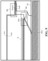
- FIG. 9 is diagram illustrating an arrangement of detection lines in a first region R 1 in FIG. 4 .
- the display panel in some embodiments includes a bonding area BA for bonding a flexible printed circuit.
- the second terminal of the second panel crack sub-loop PCSLP 2 is connected to a third pin PIN 3 in the integrated circuit IC, which is in turn connected to a fourth pin PIN 4 in the bonding area BA for bonding a flexible printed circuit.
- the second panel crack sub-loop PCSLP 2 is connected to the flexible printed circuit through the fourth pin PIN 4 .
- the crack detection circuit in some embodiments further includes a third conduction loop CLP 3 .
- the third conduction loop CLP 3 is configured to detect a crack in the display panel by measuring a resistance of the third conduction loop CLP 3 .
- a measured value of a resistance of the third conduction loop CLP 3 that is greater than a reference value indicates the presence of a line break in the third conduction loop CLP 3 , which in turn indicates the presence of a crack in the display panel.
- the third conduction loop CLP 3 is disposed in the thin film transistor array substrate, and the third conduction loop CLP 3 is configured to detect a crack in the thin film transistor array substrate.
- the third conduction loop CLP 3 is disposed in a layer adjacent to the touch control structure, and the third conduction loop CLP 3 is configured to detect a crack in layers adjacent to the touch control structure.
- the first conduction loop CLP 1 and the second conduction loop CLP 2 space apart the third conduction loop CLP 3 from the display area DA.
- a first portion of the third conduction loop CLP 3 is on a side of the first conduction loop CLP 1 away from the display area DA
- a second portion of the third conduction loop CLP 3 is on a side of the second conduction loop CLP 2 away from the display area DA.
- FIG. 5 H is a schematic diagram illustrating the structure of a third conduction loop in some embodiments according to the present disclosure.
- the third conduction loop CLP 3 continuously extends, sequentially, from a first corner region CR 1 of a first sub-area PA 1 , to a second sub-area PA 2 , to a third sub-area PA 3 , to the second sub-area PA 2 , to the first sub-area PA 1 , to a fourth sub-area PA 4 , to the third sub-area PA 3 , to the fourth sub-area PA 4 , and back to a second corner region CR 2 of the first sub-area PA 1 .
- the first sub-area PA 1 , the second sub-area PA 2 , the third sub-area PA 3 , and the fourth sub-area PA 4 are respectively sub-areas of a peripheral area PA in the display panel.
- a first terminal and a second terminal of the third conduction loop CLP 3 are respectively connected to two bonding pins (e.g., a fifth pin PIN 5 and a sixth pin PIN 6 ) in a bonding area BA for bonding a flexible printed circuit.
- the terminals of the third conduction loop CLP 3 are connected to the flexible printed circuit.
- FIG. 10 A is diagram illustrating an arrangement of detection lines in a third region R 3 in FIG. 4 .
- FIG. 10 B is a further zoom-in view of a third sub-region SR 3 in FIG. 10 A .
- FIG. 10 A and FIG. 10 B illustrate connectivity between the second touch crack detection line TCDL 2 and the first panel crack sub-loop PCSLP 1 in one example, and the arrangement of the detection lines in this region.
- FIG. 11 is diagram illustrating an arrangement of detection lines in a fourth region R 4 in FIG. 4 .
- FIG. 11 illustrates connectivity between the fourth touch crack detection line TCDL 4 and the second panel crack sub-loop PCSLP 2 in one example, and the arrangement of the detection lines in this region.
- FIG. 12 is a diagram illustrating the structure of a display apparatus in some embodiments according to the present disclosure.
- the display apparatus includes a display panel described herein; and a flexible printed circuit FPC connected to the integrated circuit IC.
- Examples of appropriate display apparatuses include, but are not limited to, an electronic paper, a mobile phone, a tablet computer, a television, a monitor, a notebook computer, a digital album, a GPS, etc.
- the display apparatus is an organic light emitting diode display apparatus.
- the display apparatus is a liquid crystal display apparatus.
- a first terminal and a second terminal of the third conduction loop CLP 3 are respectively connected to two bonding pins (e.g., PIN 5 and PIN 6 ) bonded to the flexible printed circuit.
- a second terminal of the first panel crack sub-loop PCSLP 1 is connected to a first pin PIN 1 in the integrated circuit IC, which is in turn connected to a second pin PIN 2 , the second pin PIN 2 bonded to the flexible printed circuit FPC.
- a second terminal of the second panel crack sub-loop PCSLP 2 is connected to a third pin PIN 3 in the integrated circuit IC, which is in turn connected to a fourth pin PIN 4 , the fourth pin PIN 4 bonded to the flexible printed circuit FPC.
- the present disclosure further provides a method of detecting crack in a display panel.
- the display panel includes display elements in a display area; a touch electrode layer at least partially in the display area.
- the display elements and the touch electrode layer are absent in a window region that is at least partially surrounded by the display area.
- the method includes providing a first conduction loop; electrically connecting a first terminal of the first conduction loop to an integrated circuit; electrically connecting a second terminal of the first conduction loop to a source electrode of a switching transistor; electrically connecting a drain electrode of the switching transistor to a data line; providing, by the integrated circuit, a voltage signal to the first terminal of the first conduction loop while turning on the switching transistor; and determining presence or absence of a crack in a region having the first conduction loop based on light emitting status of light emitting elements connected to the data line.
- providing the first conduction loop comprises extending a window region crack detection line of the first conduction loop into a region substantially surrounding the window region; and determining presence or absence of the crack comprises determining presence or absence of a crack in the region substantially surrounding the window region.
- providing the first conduction loop further includes extending a first touch crack detection line of the first conduction loop from a first sub-area through a second sub-area into a third sub-area of a peripheral area of the display panel, and extending a second touch crack detection line of the first conduction loop from the third sub-area through the second sub-area into the first sub-area; and determining presence or absence of the crack further comprises determining presence or absence of a crack in a touch control structure in the first sub-area, the second sub-area, and the third sub-area.
- providing the first conduction loop further includes extending a first panel crack sub-loop of the first conduction loop from a first sub-area of a peripheral area through a second sub-area into a third sub-area of a peripheral area of the display panel and back to the first sub-area; and determining presence or absence of the crack further comprises determining presence or absence of a crack in a thin film transistor array substrate in the first sub-area, the second sub-area, and the third sub-area.
- the method further includes providing a second conduction loop; electrically connecting a first terminal of the second conduction loop to an integrated circuit; electrically connecting a second terminal of the second conduction loop to a source electrode of a switching transistor; electrically connecting a drain electrode of the switching transistor to a data line; providing, by the integrated circuit, a voltage signal to the first terminal of the second conduction loop while turning on the switching transistor; and determining presence or absence of a crack in a region having the second conduction loop based on light emitting status of light emitting elements connected to the data line.
- providing the second conduction loop comprises extending a third touch crack detection line of the second conduction loop from a first sub-area through a fourth sub-area into a third sub-area of a peripheral area of the display panel, and extending a second touch crack detection line of the second conduction loop from the third sub-area through the fourth sub-area into the first sub-area; and determining presence or absence of the crack further comprises determining presence or absence of a crack in a touch control structure in the first sub-area, the fourth sub-area, and the third sub-area.
- providing the second conduction loop further includes extending a second panel crack sub-loop of the second conduction loop from a first sub-area of a peripheral area through a fourth sub-area into a third sub-area of a peripheral area of the display panel and back to the first sub-area; and determining presence or absence of the crack further comprises determining presence or absence of a crack in a thin film transistor array substrate in the first sub-area, the fourth sub-area, and the third sub-area.
- the method further includes providing a third conduction loop continuously extending, sequentially, from a first corner region of a first sub-area, to a second sub-area, to a third sub-area, to the second sub-area, to the first sub-area, to a fourth sub-area, to the third sub-area, to the fourth sub-area, and back to a second corner region of the first sub-area.
- the first sub-area, the second sub-area, the third sub-area, and the fourth sub-area are respectively sub-areas of a peripheral area in the display panel; and determining presence or absence of the crack further comprises measuring a resistance of the third conduction loop.
- the method further includes respectively connecting a first terminal and a second terminal of the third conduction loop to two bonding pins that are bonded to a flexible printed circuit.
- the present disclosure provides a touch control structure.
- the touch control structure includes a plurality of first mesh electrodes along a row direction and a plurality of second mesh electrodes along a column direction.
- the touch control structure is limited in a touch control area and absent in a window region surrounded by the touch control area.
- a window-crossing column of the plurality of second mesh electrodes includes a first mesh block and a second mesh block respectively on a first side and a second side of the window region; a first conductive plate directly connected to one or more mesh lines of the first mesh block; a second conductive plate directly connected to one or more mesh lines of the second mesh block; and a first conductive bridge connecting the first conductive plate and the second conductive plate.
- the first conductive bridge comprises a first segment and a second segment; and the second segment is in a layer different from the first segment, the first conductive plate, and the second conductive plate.
- the column direction and the row direction cross over each other.
- the column direction and the row direction are perpendicular to each other.
- the column direction and the row direction cross over each other at an inclined angle that is not 90 degrees.
- Mesh electrodes include mesh lines which typically have a line width in a range of 1 ⁇ m to 50 ⁇ m. Thus, connecting adjacent mesh blocks through the mesh lines is particularly difficult, and often resulting in poor connectivity.
- the present disclosure adopts a novel and advantageous touch electrode design that obviate issues in related touch control structures.
- FIG. 13 is a schematic diagram illustrating the structure of a touch control structure in some embodiments according to the present disclosure.
- the touch control structure in some embodiments includes a plurality of first mesh electrodes TE 1 arranged respectively in a plurality of rows and a plurality of second mesh electrodes TE 2 arranged in respectively a plurality of columns. Adjacent rows of the plurality of rows are isolated from each other. Adjacent columns of the plurality of columns are isolated from each other.
- the touch control structure is a mutual capacitance type touch control structure.
- the plurality of first mesh electrodes TE 1 are a plurality of touch scanning electrodes
- the plurality of second mesh electrodes TE 2 are a plurality of touch sensing electrodes.
- the plurality of mesh touch electrodes TE 1 are a plurality of touch sensing electrodes
- the plurality of second mesh electrodes TE 2 are a plurality of touch scanning electrodes.
- the touch control structure is in a touch control area of a display panel.
- the touch control area substantially overlaps with a display area of the display panel.
- the display panel is configured to display an image in at least a portion of the touch control area.
- the respective one of the plurality of first mesh electrodes TE 1 extends along a row direction RD; and the respective one of the plurality of second mesh electrodes TE 2 extends along a column direction CD.
- the row direction RD and the column direction CD are two non-parallel directions, for example, the row direction RD and the column direction CD cross over each other.
- the row direction RD and the column direction CD are perpendicular to each other.
- the row direction RD and the column direction CD cross over each other at an inclined angle that is not 90 degrees.
- the touch control structure is limited in a touch control area TCA and absent in a window region WR surrounded by the touch control area TCA.
- the touch control structure may be a touch control structure in a display panel, where the touch control area TCA substantially overlaps with a display area of the display panel, and the window region WR is a region in the display panel having a hole configured for installing an accessory such as a camera lens or a fingerprint sensor.
- the display panel is configured to display an image in at least a portion of the touch control area TCA.
- display elements of the display panel and the touch control structure are absent; in the display area or at least a portion of the touch control area TCA, both display elements of the display panel and the touch control structure are present.
- FIG. 14 is a zoom-in view of a touch control structure surrounding a window region in some embodiments according to the present disclosure.
- FIG. 15 is a schematic diagram illustrating a window region in some embodiments according to the present disclosure. Referring to FIG. 13 to FIG.
- a window-crossing column WCC of the plurality of second mesh electrodes TE 2 includes a first mesh block MB 1 and a second mesh block MB 2 respectively on a first side S 1 and a second side S 2 of the window region WR; a first conductive plate CP 1 directly connected to one or more mesh lines of the first mesh block MB 1 ; a second conductive plate CP 2 directly connected to one or more mesh lines of the second mesh block MB 2 ; and a first conductive bridge CB 1 connecting the first conductive plate CP 1 and the second conductive plate CP 2 .
- the first conductive bridge CB 1 includes a first segment SG 1 and a second segment SG 2 .
- the second segment SG 2 is in a layer different from the first segment SG 1 , the first conductive plate CP 1 , and the second conductive plate CP 2 .
- the second segment SG 2 is in a first layer, e.g., a first conductive material layer such as a first metallic material layer.
- the first segment SG 1 , the first conductive plate CP 1 , and the second conductive plate CP 2 are in a second layer, e.g., a second conductive material layer such as a second metallic material layer.
- FIG. 16 A is a zoom-in view of a first zoom-in region ZR 1 in FIG. 14 .
- FIG. 16 B is a cross-sectional view along an E-E′ line in FIG. 16 A .
- the first segment SG 1 is in a second layer SL 1
- the second segment SG 2 is in a first layer SL 2 .
- FIG. 16 A is a zoom-in view of a first zoom-in region ZR 1 in FIG. 14 .
- FIG. 16 B is a cross-sectional view along an E-E′ line in FIG. 16 A .
- the first segment SG 1 is in a second layer SL 1
- the second segment SG 2 is in a first layer SL 2 .
- the touch control structure includes a buffer layer BUF on a second inorganic encapsulating sub-layer CVD 2 , the second inorganic encapsulating sub-layer CVD 2 being a sub-layer of an encapsulating layer for encapsulating light emitting elements in a display apparatus having the touch control structure.
- the touch control structure further includes a first layer SL 1 on a side of the buffer layer BUF away from the second inorganic encapsulating sub-layer CVD 2 , a touch insulating layer TI on a side of the first layer SL 1 away from the buffer layer BUF, a second layer SL 2 on a side of the touch insulating layer TI away from the first layer SL 1 , and an overcoat layer OC on a side of the second layer SL 2 away from the touch insulating layer TI.
- mesh lines of the third mesh block MB 3 are in the second layer SL 2 .
- a first window-crossing row WCR 1 of the plurality of first mesh electrodes TE 1 includes a third mesh block MB 3 on a third side S 3 of the window region WR; and a third conductive plate CP 3 directly connected to one or more mesh lines of the third mesh block MB 3 .
- the third side S 3 is between the fast side S 1 and the second side S 2 .
- the third conductive plate CP 3 spaces apart the first conductive bridge CB 1 from the third mesh block MB 3 .
- FIG. 17 is a schematic diagram illustrating the structure of a third conductive plate in some embodiments according to the present disclosure.
- the third conductive plate CP 3 includes a first part 3 - 1 and a second part 3 - 2 .
- the first part has a first shortest plate width pw 1 along a direction from the first part 3 - 1 to the window region WR;
- the second part 3 - 2 has a second shortest plate width pw 2 along a direction from the second part 3 - 2 to the window region WR.
- the first shortest plate width pw 1 is less than the second shortest plate width pw 2 .
- the inventors of the present discover that, when a conductive bridge extends around a periphery of the window region, electrostatic discharge is prone to occur when the conductive bridge is in close proximity to a conductive plate directly connected to one or more mesh lines of a mesh block.
- the first conductive bridge CB 1 is in close proximity to the second part 3 - 2 of the third conductive plate CB 3 .
- the electrostatic discharge issue can be obviated by disposing a segment of the conductive bridge in close proximity to the conductive plate in a layer different from the conductive plate.
- the second segment SG 2 is in close proximity to a second part 3 - 2 of the third conductive plate CP 3 . Accordingly, in some embodiment, in the touch control structure according to the present disclosure, the second segment SG 2 is in a layer different from the third conductive plate CP 3 . Referring to FIG. 16 B , the second segment SG 2 is in the first layer SL 1 , whereas the first part 3 - 1 and the second part 3 - 2 of the third conductive plate, and the first segment SL 1 are in the second layer SL 2 .
- the first segment SG 1 and the second segment SG 2 are respectively around a first portion P 1 and a second portion P 2 of the periphery of the window region WR; the first part 3 - 1 and the second part 3 - 2 are respectively around a third portion P 3 and a fourth portion P 4 of the periphery of the window region WR; the first portion P 1 is at least partially overlapping with the third portion P 3 ; and the second portion P 2 is at least partially overlapping with the fourth portion P 4 .
- the second portion P 2 and the fourth portion P 4 substantially (e.g., 80%, 85%, 90%, 95%, 99%, or 100%) overlap with each other.
- the first portion P 1 and the third portion P 3 substantially (e.g., 80%, 85%, 90%, 95%, 99%, or 100%) overlap with each other.
- the third conductive plate further includes a third part 3 - 3 , the first part 3 - 1 between the second part 3 - 2 and the third part 3 - 3 .
- the second part 3 - 2 and the third part 3 - 3 are connected through the first part 3 - 1 .
- the second part 3 - 2 is directly connected to the first part 3 - 1
- the third part 3 - 3 is directly connected to the first part 3 - 1 .
- the first conductive plate CP 1 further includes a third segment SG 3 , the first segment SG 1 between the second segment SG 2 and the third segment SG 3
- the second segment SG 2 and the third segment SG 3 are connected through the first segment SG 1
- the second segment SG 2 is directly connected to the first segment SG 1
- the third segment SG 3 is directly connected to the first segment SG 1 .
- the second segment SG 2 and the third segment SG 3 can be formed in a same layer by simultaneously performing the step of forming the second segment SG 2 and the step of forming the third segment SG 3 .
- the term “same layer” does not always mean that the thickness of the layer or the height of the layer in a cross-sectional view is the same.
- FIG. 18 A is a zoom-in view of a second zoom-in region ZR 2 in FIG. 14 .
- FIG. 18 B is a cross-sectional view along an F-F′ line in FIG. 18 A .
- the second segment SG 2 and the third segment SG 3 are in the first layer SL 1 .
- the first segment SG 1 , the first part 3 - 1 , the second part 3 - 2 , the third part 3 - 3 , mesh lines of the third mesh block MB 3 are in the second layer SL 2 .
- the first part has a first shortest plate width pw 1 along a direction from the first part 3 - 1 to the window region WR;
- the second part 3 - 2 has a second shortest plate width pw 2 along a direction from the second part 3 - 2 to the window region WR;
- the third part 3 - 3 has a third shortest plate width pw 3 along a direction from the third part 3 - 3 to the window region WR.
- the first shortest plate width pw 1 is less than the second shortest plate width pw 2 ; and the first shortest plate width pw 1 is less than the third shortest plate width pw 3 .
- the touch control structure in some embodiments further includes a first dummy plate DP 1 insulated from the first conductive bridge CB 1 and the third conductive plate CP 3 , and spacing part a portion of the first conductive bridge CB 1 and a portion of the third conductive plate CP 3 .
- the first dummy plate DP 1 is around a seventh portion P 7 of the periphery of the window region WR.
- the seventh portion P 7 is at least partially overlapping with the third portion P 3 , and is non-overlapping with the fourth portion P 4 and the sixth portion P 6 .
- the third portion P 3 and the seventh portion P 7 substantially (e.g., 80%, 85%, 90%, 95%, 99%, or 100%) overlap with each other.
- an orthographic projection of a conductive component on the base substrate is absent in a space between an orthographic projection of the second segment SG 2 on the base substrate and an orthographic projection of the second part 3 - 2 on the base substrate.
- an orthographic projection of a conductive component on the base substrate is absent in a space between an orthographic projection of the third segment SG 3 on the base substrate and an orthographic projection of the third part 3 - 3 on the base substrate.
- an orthographic projection of the first dummy plate DP 1 on the base substrate is in a space between an orthographic projection of the first segment SG 1 on the base substrate and an orthographic projection of the first part 3 - 1 on the base substrate.
- a second window-crossing row WCR 2 of the plurality of first mesh electrodes TE 1 includes a fourth mesh block MB 4 and a fifth mesh block MB 5 respectively on a fourth side S 4 ants a fifth side S 5 of the window region.
- the second side S 2 is between the fourth side S 4 and the fifth side S 5 .
- the fifth side S 5 is between the second side S 2 and the third side S 3 .
- the fourth side S 4 is between the first side S 1 and the second side S 2 .
- the second window-crossing row WCR 2 of the plurality of first mesh electrodes TE 1 further includes a fourth conductive plate CP 4 directly connected to one or more mesh lines of the fourth mesh block MB 4 ; a fifth conductive plate CP 5 directly connected to one or more mesh lines of the fifth mesh block MB 5 ; and a second conductive bridge CB 2 connecting the fourth conductive plate CP 4 and the fifth conductive plate CP 5 .
- the first conductive plate CP 1 is around an eighth portion P 8 of the periphery of the window region WR and the second conductive bridge CB 2 is around a ninth portion P 9 of the periphery of the window region WR.
- the eighth portion P 8 is at least partially overlapping with the ninth portion P 9 .
- the eighth portion P 8 and the ninth portion P 9 substantially (e.g., 80%, 85%, 90%, 95%, 99%, or 100%) overlap with each other.
- the fourth segment SG 4 is in a same layer as the second segment SG 2 and the third segment SG 3 , and is in a layer different from the first segment SG 1 , the first conductive plate CP 1 , the second conductive plate CP 2 , and the third conductive plate CP 3 .
- the fourth segment SG 4 is in a layer different from the first segment SG 1 , the first conductive plate CP 1 , the second conductive plate CP 2 , the fourth conductive plate CP 4 , the fifth conductive plate CP 5 , and the second conductive bridge CB 2 optionally, mesh lines of the fifth mesh block MB 5 are in the second layer SL 2 .
- the first conductive bridge in some embodiments further includes a fifth segment SG 5 between the fourth segment SG 4 and the second segment SG 2 .
- the second segment SG 2 and the fourth segment SG 4 are connected through the fifth segment SG 5 .
- the second segment SG 2 is directly connected to the fifth segment SG 5
- the fourth segment SG 4 is directly connected to the fifth segment SG 5 .
- FIG. 21 is a cross-sectional view along an H-H′ line in FIG. 19 .
- the fifth segment SG 5 is directly connected to the fourth segment SG 4 through a via v extending through the touch insulating layer TI.
- the connections between other respective segments of the first conductive bridge CB 1 can be similarly implemented.
- the connection between the first segment SG 1 and the second segment SG 2 , the connection between the first segment SG 1 and the third segment SG 3 , or the connection between the second segment SG 2 and the fits segment SG 5 can be implemented by respective vias extending through the touch insulating layer TI.
- the fifth segment SG 5 is in a same layer as the first segment SG 1 , the first conductive plate CP 1 , the second conductive plate CP 2 , the third conductive plate CP 3 , and the second conductive bridge CB 2 .
- the fifth segment SG 5 is in a layer different from the second segment SG 2 and the fourth segment SG 4 .
- the touch control structure further includes a second dummy plate DP 2 insulated from the fifth conductive plate CP 5 and the fifth segment SG 5 , and spacing part a portion of the fifth conductive plate CP 5 and a portion of the fifth segment SG 5 .
- the fifth segment SG 5 is around a tenth portion P 10 of the periphery of the window region WR.
- the second dummy plate DP 2 is around an eleventh portion P 11 of the periphery of the window region WR.
- the tenth portion P 10 is at least partially overlapping with the eleventh portion P 11 .
- a sub-portion of the tenth portion P 10 is non-overlapping with the eleventh portion P 11 .
- the touch control structure in some embodiments further includes a third dummy plate DP 3 around a twelfth portion P 12 of the periphery of the window region WR.
- the twelfth portion P 12 is between the eleventh portion P 11 and the second portion.
- the twelfth portion P 12 is non-overlapping with the eleventh portion P 11 , and is non-overlapping with the second portion P 2 .
- the twelfth portion P 12 is at least partially overlapping with the tenth portion P 10 .
- a combination of the eleventh portion P 11 and the twelfth portion P 12 substantially (e.g., 80%, 85%, 90%, 95%, 99%, or 100%) overlap with the tenth portion P 10 .
- the touch control structure in some embodiments further includes a protective ring PR substantially (e.g., 80%, 85%, 90%, 95%, 99%, or 100%) surrounding the window region WR.
- a protective ring PR substantially (e.g., 80%, 85%, 90%, 95%, 99%, or 100%) surrounding the window region WR.
- the first conductive plate CP 1 , the second conductive plate CP 2 , and the first conductive bridge CB 1 are respectively around portions of the protective ring PR.
- the protective ring PR is in a same layer as the second segment SG 2 , the third segment SG 3 , and the fourth segment SG 4 .
- the protective ring PR is in a layer different from the first segment SG 1 , the fifth segment SG 5 , the first conductive plate CP 1 , the second conductive plate CP 2 , the third conductive plate CP 3 , the fourth conductive plate CP 4 , and the fifth conductive plate CP 5 .
- the touch control structure in some embodiments further includes a detection line DTL substantially (e.g., 80%, 85%, 90%, 95%, 99%, or 100%) surrounding the window region WR.
- FIG. 5 B is a schematic diagram illustrating the structure of a detection line in some embodiments according to the present disclosure. Referring to FIG. 14 and FIG.
- the detection line DTL includes contiguously a first line portion LP 1 extending clock-wisely around a first half (e.g., a right half) of a periphery of the window region WR, a second line portion LP 2 extending counter-clock-wisely around the first half of the periphery of the window region WR and a second half of the periphery of the window region WR 2 , and a third line portion LP 3 extending clock-wisely around the second half of the periphery of the window region WR.
- first half and “second half” is not limited to exact half, but also include less than half or greater than half.
- the touch control structure in some embodiments further includes a sixth mesh block MBC 1 and a seventh mesh block MBC 2 respectively on two sides of the first mesh block MB 1 ; and a first lead line LL 1 connecting the sixth mesh block MBC 1 to the third line portion LP 3 ; and a second lead line LL 2 connecting the seventh mesh block MBC 2 to the first line portion LP 1 .
- the first line portion LP 1 , the second line portion LP 2 , the third line portion LP 3 are in a same layer as the first segment SG 1 , the fifth segment SG 5 , the first conductive plate CP 1 , the second conductive plate CP 2 , the third conductive plate CP 3 , the fourth conductive plate CP 4 , and the fifth conductive plate CP 5 .
- the first lead line LL 1 and the second lead line LL 2 are in a same layer as the second segment SG 2 , the third segment SG 3 , and the fourth segment SG 4 .
- the first conductive bridge CB 1 (or segments thereof) has a line width in a range of 5 ⁇ m to 15 ⁇ m, e.g., 5 ⁇ m to 7 ⁇ m, 7 ⁇ m to 9 ⁇ m, 9 ⁇ m to 11 ⁇ m, 11 ⁇ m to 13 ⁇ m, or 13 ⁇ m to 15 ⁇ m.
- the first conductive bridge CB 1 (or segments thereof) has a line width of 10 ⁇ m.
- the second conductive bridge CB 2 (or segments thereof) has a line width in a range of 10 ⁇ m to 20 ⁇ m, e.g., 10 ⁇ m to 12 ⁇ m, 12 ⁇ m to 14 ⁇ m, 14 ⁇ m to 16 ⁇ m, 16 ⁇ m to 18 ⁇ m, or 18 ⁇ m to 20 ⁇ m.
- the second conductive bridge CB 2 (or segments thereof) has a line width of 15 ⁇ m.
- the first shortest plate width pw 1 is in a range of 20 ⁇ m to 40 ⁇ m, e.g., 20 ⁇ m to 25 ⁇ m, 25 ⁇ m to 30 ⁇ m, 30 ⁇ m to 35 ⁇ m, or 35 ⁇ m to 40 ⁇ m.
- the first shortest plate width pw 1 is 30 ⁇ m.
- the second shortest plate width pw 2 is in a range of 75 ⁇ m to 115 ⁇ m, e.g., 75 ⁇ m to 85 ⁇ m, 85 ⁇ m to 95 ⁇ m, 95 ⁇ m to 105 ⁇ m, or 105 ⁇ m to 115 ⁇ m.
- the second shortest plate width pw 2 is 95 ⁇ m.
- the third shortest plate width pw 3 is in a range of 75 ⁇ m to 115 ⁇ m, e.g., 75 ⁇ m to 85 ⁇ m, 85 ⁇ m to 95 ⁇ m, 95 ⁇ m to 105 ⁇ m, or 105 ⁇ m to 115 ⁇ m.
- the third shortest plate width pw 3 is 95 ⁇ m.
- a ratio of the first shortest plate width pw 1 to the second shortest plate width pw 2 is a range of 1:2 to 1:4, e.g., 1:2 to 1:2.5, 1:2.5 to 1:3, 1:3 to 1:3.5, or 1:3.5 to 1:4.
- a ratio of the first shortest plate width pw 1 to the third shortest plate width pw 3 is a range of 1:2 to 1:4, e.g., 1:2 to 1:2.5, 1:2.5 to 1:3, 1:3 to 1:3.5, or 1:3.5 to 1:4.
- the first conductive plate has a shortest plate width along a direction from the first conductive plate to the window region in a range of 80 ⁇ m to 160 ⁇ m, e.g., 80 ⁇ m to 100 ⁇ m, 100 ⁇ m to 120 ⁇ m, 120 ⁇ m to 140 ⁇ m, or 140 ⁇ m to 160 ⁇ m.
- the shortest plate width is 120 ⁇ m.
- the second conductive plate has a shortest plate width along a direction from the second conductive plate to the window region in a range of 80 ⁇ m to 160 ⁇ m, e.g., 80 ⁇ m to 100 ⁇ m, 100 ⁇ m to 120 ⁇ m, 120 ⁇ m to 140 ⁇ m, or 140 ⁇ m to 160 ⁇ m.
- the shortest plate width is 120 ⁇ m.
- the first dummy plate has a shortest plate width along a direction from the first dummy plate to the window region in a range of 30 ⁇ m to 70 ⁇ m, e.g., 30 ⁇ m to 40 ⁇ m, 40 ⁇ m to 50 ⁇ m, 50 ⁇ m to 60 ⁇ m, or 60 ⁇ m to 70 ⁇ m.
- the shortest plate width is 50 ⁇ m.
- the second dummy plate has a shortest plate width along a direction from the second dummy plate to the window region in a range of 20 ⁇ m to 40 ⁇ m, e.g., 20 ⁇ m to 25 ⁇ m, 25 ⁇ m to 30 ⁇ m, 30 ⁇ m to 35 ⁇ m, or 35 ⁇ m to 40 ⁇ m.
- the shortest plate width is 30 ⁇ m.
- the fourth conductive plate has a shortest plate width along a direction from the fourth conductive plate to the window region in a range of 5 ⁇ m to 15 ⁇ m, e.g., 5 ⁇ m to 7 ⁇ m, 7 ⁇ m to 9 ⁇ m, 9 ⁇ m to 11 ⁇ m, 11 ⁇ m to 13 ⁇ m, or 13 ⁇ m to 15 ⁇ m.
- the shortest plate width is 10 ⁇ m.
- the fifth conductive plate has a shortest plate width along a direction from the fifth conductive plate to the window region in a range of 30 ⁇ m to 70 ⁇ m, e.g., 30 ⁇ m to 40 ⁇ m, 40 ⁇ m to 50 ⁇ m, 50 ⁇ m to 60 ⁇ m, or 60 ⁇ m to 70 ⁇ m.
- the shortest plate width is 50 ⁇ m.
- the protective ring has a shortest plate width along a direction from the protective ring to the window region in a range of 25 ⁇ m to 65 ⁇ m, e.g., 25 ⁇ m to 35 ⁇ m, 35 ⁇ m to 45 ⁇ m, 45 ⁇ m to 55 ⁇ m, or 55 ⁇ m to 65 ⁇ m.
- the shortest plate width is 45 ⁇ m.
- the detection line (or line portions thereof) has a line width in a range of 2.5 ⁇ m to 6.5 ⁇ m, e.g., 2.5 ⁇ m to 3.5 ⁇ m, 3.5 ⁇ m to 4.5 ⁇ m, 4.5 ⁇ m to 5.5 ⁇ m, or 5.5 ⁇ m to 6.5 ⁇ m.
- the first conductive bridge CB 1 (or segments thereof) has a line width of 4.5 ⁇ m.
- the first lead line or the second lead line has a line width in a range of 5 ⁇ m to 15 ⁇ m, e.g., 5 ⁇ m to 7 ⁇ m, 7 ⁇ m to 9 ⁇ m, 9 ⁇ m to 11 ⁇ m, 11 ⁇ m to 13 ⁇ m, or 13 ⁇ m to 15 ⁇ m.
- the first lead line or the second lead line has a line width of 10 ⁇ m.
- the term “the invention”, “the present invention” or the like does not necessarily limit the claim scope to a specific embodiment, and the reference to exemplary embodiments of the invention does not imply a limitation on the invention, and no such limitation is to be inferred.
- the invention is limited only by the spirit and scope of the appended claims. Moreover, these claims may refer to use “first”, “second”, etc. following with noun or element. Such terms should be understood as a nomenclature and should not be construed as giving the limitation on the number of the elements modified by such nomenclature unless specific number has been given. Any advantages and benefits described may not apply to all embodiments of the invention.
Landscapes
- Engineering & Computer Science (AREA)
- Physics & Mathematics (AREA)
- General Physics & Mathematics (AREA)
- Computer Hardware Design (AREA)
- Theoretical Computer Science (AREA)
- Aviation & Aerospace Engineering (AREA)
- Microelectronics & Electronic Packaging (AREA)
- Devices For Indicating Variable Information By Combining Individual Elements (AREA)
- Position Input By Displaying (AREA)
Abstract
Description
Claims (19)
Priority Applications (1)
| Application Number | Priority Date | Filing Date | Title |
|---|---|---|---|
| US19/007,792 US20250148945A1 (en) | 2021-01-15 | 2025-01-02 | Display panel, display apparatus, and method of detecting crack in display panel |
Applications Claiming Priority (1)
| Application Number | Priority Date | Filing Date | Title |
|---|---|---|---|
| PCT/CN2021/072262 WO2022151392A1 (en) | 2021-01-15 | 2021-01-15 | Display panel, display apparatus, and method of detecting crack in display panel |
Related Parent Applications (1)
| Application Number | Title | Priority Date | Filing Date |
|---|---|---|---|
| PCT/CN2021/072262 A-371-Of-International WO2022151392A1 (en) | 2021-01-15 | 2021-01-15 | Display panel, display apparatus, and method of detecting crack in display panel |
Related Child Applications (1)
| Application Number | Title | Priority Date | Filing Date |
|---|---|---|---|
| US19/007,792 Continuation US20250148945A1 (en) | 2021-01-15 | 2025-01-02 | Display panel, display apparatus, and method of detecting crack in display panel |
Publications (2)
| Publication Number | Publication Date |
|---|---|
| US20230134939A1 US20230134939A1 (en) | 2023-05-04 |
| US12211406B2 true US12211406B2 (en) | 2025-01-28 |
Family
ID=82446855
Family Applications (2)
| Application Number | Title | Priority Date | Filing Date |
|---|---|---|---|
| US17/606,432 Active US12211406B2 (en) | 2021-01-15 | 2021-01-15 | Display panel having crack detection circuit with conduction loop, display apparatus, and method of detecting crack in display panel |
| US19/007,792 Pending US20250148945A1 (en) | 2021-01-15 | 2025-01-02 | Display panel, display apparatus, and method of detecting crack in display panel |
Family Applications After (1)
| Application Number | Title | Priority Date | Filing Date |
|---|---|---|---|
| US19/007,792 Pending US20250148945A1 (en) | 2021-01-15 | 2025-01-02 | Display panel, display apparatus, and method of detecting crack in display panel |
Country Status (3)
| Country | Link |
|---|---|
| US (2) | US12211406B2 (en) |
| EP (1) | EP4128203B1 (en) |
| WO (1) | WO2022151392A1 (en) |
Families Citing this family (3)
| Publication number | Priority date | Publication date | Assignee | Title |
|---|---|---|---|---|
| CN111509026B (en) * | 2020-05-27 | 2023-02-07 | 京东方科技集团股份有限公司 | Display panel, method for detecting cracks thereof, and display device |
| CN116612705B (en) * | 2023-05-18 | 2026-01-09 | 武汉天马微电子有限公司 | Display panel and its crack detection method, display device |
| KR20250100105A (en) | 2023-12-26 | 2025-07-03 | 엘지디스플레이 주식회사 | Display device |
Citations (25)
| Publication number | Priority date | Publication date | Assignee | Title |
|---|---|---|---|---|
| US20130082843A1 (en) | 2011-09-30 | 2013-04-04 | Apple Inc. | Detection of fracture of display panel or other patterned device |
| US20180166525A1 (en) | 2016-12-08 | 2018-06-14 | Samsung Display Co. Ltd. | Display device |
| US20190027076A1 (en) | 2017-07-18 | 2019-01-24 | Samsung Display Co., Ltd. | Display device |
| US10282003B2 (en) * | 2015-04-09 | 2019-05-07 | Samsung Display Co., Ltd. | Display device with touch sensor |
| CN109752421A (en) | 2019-01-31 | 2019-05-14 | 厦门天马微电子有限公司 | Display panel and display device |
| CN109872634A (en) | 2019-03-28 | 2019-06-11 | 武汉华星光电半导体显示技术有限公司 | A kind of display panel |
| CN109901747A (en) | 2019-02-26 | 2019-06-18 | 上海天马微电子有限公司 | Display panels and display devices |
| CN109979366A (en) | 2019-04-10 | 2019-07-05 | 京东方科技集团股份有限公司 | A kind of OLED display panel and its detection method, display device |
| CN110634411A (en) | 2019-11-07 | 2019-12-31 | 京东方科技集团股份有限公司 | A display module and packaging inspection method thereof |
| CN111048021A (en) | 2020-01-02 | 2020-04-21 | 京东方科技集团股份有限公司 | Display device, display panel and detection method thereof |
| US20200133415A1 (en) | 2018-10-26 | 2020-04-30 | Samsung Display Co., Ltd. | Display device |
| CN111106151A (en) | 2019-12-09 | 2020-05-05 | 武汉华星光电半导体显示技术有限公司 | Electronic device |
| US20200143722A1 (en) | 2018-11-02 | 2020-05-07 | Samsung Display Co., Ltd. | Display device and method for inspection thereof |
| CN111128064A (en) | 2020-01-21 | 2020-05-08 | 京东方科技集团股份有限公司 | Detection circuit and display panel |
| US20200161406A1 (en) | 2018-11-15 | 2020-05-21 | Samsung Display Co., Ltd. | Display device and inspecting method thereof |
| US20200175901A1 (en) * | 2018-11-30 | 2020-06-04 | Samsung Display Co., Ltd. | Electronic device including crack detection wiring |
| US20200173949A1 (en) | 2018-11-30 | 2020-06-04 | Samsung Display Co., Ltd. | Electronic panel and electronic apparatus comprising the same |
| CN111398355A (en) | 2020-03-25 | 2020-07-10 | 武汉华星光电半导体显示技术有限公司 | Display panel detection circuit and display device |
| CN111509026A (en) | 2020-05-27 | 2020-08-07 | 京东方科技集团股份有限公司 | Display panel, crack detection method thereof and display device |
| US10997883B2 (en) * | 2018-10-05 | 2021-05-04 | Samsung Display Co., Ltd. | Display panel crack detector, display device, and method for driving display device |
| US11276351B2 (en) * | 2019-02-19 | 2022-03-15 | Samsung Display Co., Ltd. | Display device |
| US11360625B2 (en) * | 2019-09-30 | 2022-06-14 | Wuhan China Star Optoelectronics Semiconductor Display Technology Co., Ltd. | Display device and terminal |
| US20220209187A1 (en) * | 2020-12-30 | 2022-06-30 | Samsung Display Co., Ltd. | Display panel |
| US11640218B2 (en) * | 2021-07-30 | 2023-05-02 | Shanghai Tianma Micro-electronics Co., Ltd. | Display panel, driving method of display panel, and display device |
| US11961432B2 (en) * | 2019-10-14 | 2024-04-16 | Samsung Display Co., Ltd. | Display device |
-
2021
- 2021-01-15 US US17/606,432 patent/US12211406B2/en active Active
- 2021-01-15 EP EP21918596.4A patent/EP4128203B1/en active Active
- 2021-01-15 WO PCT/CN2021/072262 patent/WO2022151392A1/en not_active Ceased
-
2025
- 2025-01-02 US US19/007,792 patent/US20250148945A1/en active Pending
Patent Citations (31)
| Publication number | Priority date | Publication date | Assignee | Title |
|---|---|---|---|---|
| US20130082843A1 (en) | 2011-09-30 | 2013-04-04 | Apple Inc. | Detection of fracture of display panel or other patterned device |
| US10282003B2 (en) * | 2015-04-09 | 2019-05-07 | Samsung Display Co., Ltd. | Display device with touch sensor |
| US20180166525A1 (en) | 2016-12-08 | 2018-06-14 | Samsung Display Co. Ltd. | Display device |
| CN108172593A (en) | 2016-12-08 | 2018-06-15 | 三星显示有限公司 | Display device |
| US20190027076A1 (en) | 2017-07-18 | 2019-01-24 | Samsung Display Co., Ltd. | Display device |
| US10997883B2 (en) * | 2018-10-05 | 2021-05-04 | Samsung Display Co., Ltd. | Display panel crack detector, display device, and method for driving display device |
| US20200133415A1 (en) | 2018-10-26 | 2020-04-30 | Samsung Display Co., Ltd. | Display device |
| CN111106143A (en) | 2018-10-26 | 2020-05-05 | 三星显示有限公司 | display device |
| CN111146247A (en) | 2018-11-02 | 2020-05-12 | 三星显示有限公司 | Display device and its inspection method |
| US20200143722A1 (en) | 2018-11-02 | 2020-05-07 | Samsung Display Co., Ltd. | Display device and method for inspection thereof |
| CN111189618A (en) | 2018-11-15 | 2020-05-22 | 三星显示有限公司 | Display apparatus and inspection method of the same |
| US20200161406A1 (en) | 2018-11-15 | 2020-05-21 | Samsung Display Co., Ltd. | Display device and inspecting method thereof |
| US20200173949A1 (en) | 2018-11-30 | 2020-06-04 | Samsung Display Co., Ltd. | Electronic panel and electronic apparatus comprising the same |
| US20200175901A1 (en) * | 2018-11-30 | 2020-06-04 | Samsung Display Co., Ltd. | Electronic device including crack detection wiring |
| CN109752421A (en) | 2019-01-31 | 2019-05-14 | 厦门天马微电子有限公司 | Display panel and display device |
| US11276351B2 (en) * | 2019-02-19 | 2022-03-15 | Samsung Display Co., Ltd. | Display device |
| CN109901747A (en) | 2019-02-26 | 2019-06-18 | 上海天马微电子有限公司 | Display panels and display devices |
| US20200273919A1 (en) | 2019-02-26 | 2020-08-27 | Shanghai Tianma Micro-electronics Co., Ltd. | Display panel and display apparatus |
| CN109872634A (en) | 2019-03-28 | 2019-06-11 | 武汉华星光电半导体显示技术有限公司 | A kind of display panel |
| US20200410913A1 (en) | 2019-03-28 | 2020-12-31 | Wuhan China Star Optoelectronics Semiconductor Display Technology Co., Ltd. | Display panel |
| CN109979366A (en) | 2019-04-10 | 2019-07-05 | 京东方科技集团股份有限公司 | A kind of OLED display panel and its detection method, display device |
| US11360625B2 (en) * | 2019-09-30 | 2022-06-14 | Wuhan China Star Optoelectronics Semiconductor Display Technology Co., Ltd. | Display device and terminal |
| US11961432B2 (en) * | 2019-10-14 | 2024-04-16 | Samsung Display Co., Ltd. | Display device |
| CN110634411A (en) | 2019-11-07 | 2019-12-31 | 京东方科技集团股份有限公司 | A display module and packaging inspection method thereof |
| CN111106151A (en) | 2019-12-09 | 2020-05-05 | 武汉华星光电半导体显示技术有限公司 | Electronic device |
| CN111048021A (en) | 2020-01-02 | 2020-04-21 | 京东方科技集团股份有限公司 | Display device, display panel and detection method thereof |
| CN111128064A (en) | 2020-01-21 | 2020-05-08 | 京东方科技集团股份有限公司 | Detection circuit and display panel |
| CN111398355A (en) | 2020-03-25 | 2020-07-10 | 武汉华星光电半导体显示技术有限公司 | Display panel detection circuit and display device |
| CN111509026A (en) | 2020-05-27 | 2020-08-07 | 京东方科技集团股份有限公司 | Display panel, crack detection method thereof and display device |
| US20220209187A1 (en) * | 2020-12-30 | 2022-06-30 | Samsung Display Co., Ltd. | Display panel |
| US11640218B2 (en) * | 2021-07-30 | 2023-05-02 | Shanghai Tianma Micro-electronics Co., Ltd. | Display panel, driving method of display panel, and display device |
Non-Patent Citations (3)
| Title |
|---|
| First Office Action in the Chinese Patent Application No. 202120110662.X, dated Jul. 7, 2021; English translation attached. |
| International Search Report & Written Opinion mailed Oct. 11, 2021, regarding PCT/CN2021/072262. |
| The Extended European Search Report in the European Patent Application No. 21918596.4, dated May 3, 2023. |
Also Published As
| Publication number | Publication date |
|---|---|
| EP4128203B1 (en) | 2026-03-11 |
| EP4128203A1 (en) | 2023-02-08 |
| US20230134939A1 (en) | 2023-05-04 |
| WO2022151392A1 (en) | 2022-07-21 |
| US20250148945A1 (en) | 2025-05-08 |
| EP4128203A4 (en) | 2023-05-31 |
Similar Documents
| Publication | Publication Date | Title |
|---|---|---|
| US20250148945A1 (en) | Display panel, display apparatus, and method of detecting crack in display panel | |
| US12461625B2 (en) | Touch control structure and display apparatus with signal lines in double and single layer structures in sub-areas of the peripheral area | |
| US20250216994A1 (en) | Touch display panel and display apparatus | |
| US11941217B2 (en) | Touch control structure, display panel, display apparatus, and method of fabricating touch control structure | |
| US11954277B2 (en) | Display panel and display apparatus | |
| CN215642639U (en) | Touch structure and display device | |
| US20250110596A1 (en) | Display panel and display apparatus | |
| US12050743B2 (en) | Display panel, display apparatus, and method of fabricating display panel | |
| CN215117062U (en) | Display panel and display device | |
| US12535925B2 (en) | Touch control structure and display apparatus | |
| US12216849B2 (en) | Display panel and display apparatus having crack detection circuit with conductive loop | |
| US12164737B2 (en) | Touch control structure and display apparatus | |
| CN114764200B (en) | Display panel, display device, and method of detecting cracks in display panel | |
| US12019834B2 (en) | Touch control structure and display apparatus | |
| CN116027928B (en) | Touch structure and display device |
Legal Events
| Date | Code | Title | Description |
|---|---|---|---|
| FEPP | Fee payment procedure |
Free format text: ENTITY STATUS SET TO UNDISCOUNTED (ORIGINAL EVENT CODE: BIG.); ENTITY STATUS OF PATENT OWNER: LARGE ENTITY |
|
| STPP | Information on status: patent application and granting procedure in general |
Free format text: APPLICATION UNDERGOING PREEXAM PROCESSING |
|
| AS | Assignment |
Owner name: BOE TECHNOLOGY GROUP CO., LTD., CHINA Free format text: ASSIGNMENT OF ASSIGNORS INTEREST;ASSIGNORS:ZHANG, SHUN;ZHANG, YUANQI;WEN, PING;AND OTHERS;REEL/FRAME:057946/0328 Effective date: 20210629 Owner name: CHENGDU BOE OPTOELECTRONICS TECHNOLOGY CO., LTD., CHINA Free format text: ASSIGNMENT OF ASSIGNORS INTEREST;ASSIGNORS:ZHANG, SHUN;ZHANG, YUANQI;WEN, PING;AND OTHERS;REEL/FRAME:057946/0328 Effective date: 20210629 |
|
| STCB | Information on status: application discontinuation |
Free format text: ABANDONED -- INCOMPLETE APPLICATION (PRE-EXAMINATION) |
|
| STPP | Information on status: patent application and granting procedure in general |
Free format text: APPLICATION UNDERGOING PREEXAM PROCESSING |
|
| STPP | Information on status: patent application and granting procedure in general |
Free format text: DOCKETED NEW CASE - READY FOR EXAMINATION |
|
| STPP | Information on status: patent application and granting procedure in general |
Free format text: NON FINAL ACTION MAILED |
|
| STPP | Information on status: patent application and granting procedure in general |
Free format text: RESPONSE TO NON-FINAL OFFICE ACTION ENTERED AND FORWARDED TO EXAMINER |
|
| STPP | Information on status: patent application and granting procedure in general |
Free format text: NOTICE OF ALLOWANCE MAILED -- APPLICATION RECEIVED IN OFFICE OF PUBLICATIONS |
|
| STPP | Information on status: patent application and granting procedure in general |
Free format text: PUBLICATIONS -- ISSUE FEE PAYMENT VERIFIED |
|
| STCF | Information on status: patent grant |
Free format text: PATENTED CASE |