US12205529B2 - Display apparatus - Google Patents
Display apparatus Download PDFInfo
- Publication number
- US12205529B2 US12205529B2 US18/179,937 US202318179937A US12205529B2 US 12205529 B2 US12205529 B2 US 12205529B2 US 202318179937 A US202318179937 A US 202318179937A US 12205529 B2 US12205529 B2 US 12205529B2
- Authority
- US
- United States
- Prior art keywords
- layer
- display
- area
- driving circuit
- display apparatus
- Prior art date
- Legal status (The legal status is an assumption and is not a legal conclusion. Google has not performed a legal analysis and makes no representation as to the accuracy of the status listed.)
- Active
Links
Images


Classifications
-
- G—PHYSICS
- G09—EDUCATION; CRYPTOGRAPHY; DISPLAY; ADVERTISING; SEALS
- G09F—DISPLAYING; ADVERTISING; SIGNS; LABELS OR NAME-PLATES; SEALS
- G09F9/00—Indicating arrangements for variable information in which the information is built-up on a support by selection or combination of individual elements
- G09F9/30—Indicating arrangements for variable information in which the information is built-up on a support by selection or combination of individual elements in which the desired character or characters are formed by combining individual elements
- G09F9/301—Indicating arrangements for variable information in which the information is built-up on a support by selection or combination of individual elements in which the desired character or characters are formed by combining individual elements flexible foldable or roll-able electronic displays, e.g. thin LCD, OLED
-
- G—PHYSICS
- G06—COMPUTING OR CALCULATING; COUNTING
- G06F—ELECTRIC DIGITAL DATA PROCESSING
- G06F1/00—Details not covered by groups G06F3/00 - G06F13/00 and G06F21/00
- G06F1/16—Constructional details or arrangements
- G06F1/1613—Constructional details or arrangements for portable computers
- G06F1/1615—Constructional details or arrangements for portable computers with several enclosures having relative motions, each enclosure supporting at least one I/O or computing function
- G06F1/1624—Constructional details or arrangements for portable computers with several enclosures having relative motions, each enclosure supporting at least one I/O or computing function with sliding enclosures, e.g. sliding keyboard or display
-
- G—PHYSICS
- G01—MEASURING; TESTING
- G01B—MEASURING LENGTH, THICKNESS OR SIMILAR LINEAR DIMENSIONS; MEASURING ANGLES; MEASURING AREAS; MEASURING IRREGULARITIES OF SURFACES OR CONTOURS
- G01B7/00—Measuring arrangements characterised by the use of electric or magnetic techniques
- G01B7/16—Measuring arrangements characterised by the use of electric or magnetic techniques for measuring the deformation in a solid, e.g. by resistance strain gauge
- G01B7/18—Measuring arrangements characterised by the use of electric or magnetic techniques for measuring the deformation in a solid, e.g. by resistance strain gauge using change in resistance
-
- G—PHYSICS
- G06—COMPUTING OR CALCULATING; COUNTING
- G06F—ELECTRIC DIGITAL DATA PROCESSING
- G06F1/00—Details not covered by groups G06F3/00 - G06F13/00 and G06F21/00
- G06F1/16—Constructional details or arrangements
- G06F1/1613—Constructional details or arrangements for portable computers
- G06F1/1633—Constructional details or arrangements of portable computers not specific to the type of enclosures covered by groups G06F1/1615 - G06F1/1626
- G06F1/1637—Details related to the display arrangement, including those related to the mounting of the display in the housing
- G06F1/1652—Details related to the display arrangement, including those related to the mounting of the display in the housing the display being flexible, e.g. mimicking a sheet of paper, or rollable
-
- G—PHYSICS
- G06—COMPUTING OR CALCULATING; COUNTING
- G06F—ELECTRIC DIGITAL DATA PROCESSING
- G06F1/00—Details not covered by groups G06F3/00 - G06F13/00 and G06F21/00
- G06F1/16—Constructional details or arrangements
- G06F1/1613—Constructional details or arrangements for portable computers
- G06F1/1633—Constructional details or arrangements of portable computers not specific to the type of enclosures covered by groups G06F1/1615 - G06F1/1626
- G06F1/1675—Miscellaneous details related to the relative movement between the different enclosures or enclosure parts
- G06F1/1677—Miscellaneous details related to the relative movement between the different enclosures or enclosure parts for detecting open or closed state or particular intermediate positions assumed by movable parts of the enclosure, e.g. detection of display lid position with respect to main body in a laptop, detection of opening of the cover of battery compartment
-
- G—PHYSICS
- G06—COMPUTING OR CALCULATING; COUNTING
- G06F—ELECTRIC DIGITAL DATA PROCESSING
- G06F1/00—Details not covered by groups G06F3/00 - G06F13/00 and G06F21/00
- G06F1/16—Constructional details or arrangements
- G06F1/1613—Constructional details or arrangements for portable computers
- G06F1/1633—Constructional details or arrangements of portable computers not specific to the type of enclosures covered by groups G06F1/1615 - G06F1/1626
- G06F1/1675—Miscellaneous details related to the relative movement between the different enclosures or enclosure parts
- G06F1/1681—Details related solely to hinges
-
- G—PHYSICS
- G09—EDUCATION; CRYPTOGRAPHY; DISPLAY; ADVERTISING; SEALS
- G09G—ARRANGEMENTS OR CIRCUITS FOR CONTROL OF INDICATING DEVICES USING STATIC MEANS TO PRESENT VARIABLE INFORMATION
- G09G3/00—Control arrangements or circuits, of interest only in connection with visual indicators other than cathode-ray tubes
- G09G3/03—Control arrangements or circuits, of interest only in connection with visual indicators other than cathode-ray tubes specially adapted for displays having non-planar surfaces, e.g. curved displays
- G09G3/035—Control arrangements or circuits, of interest only in connection with visual indicators other than cathode-ray tubes specially adapted for displays having non-planar surfaces, e.g. curved displays for flexible display surfaces
-
- G—PHYSICS
- G09—EDUCATION; CRYPTOGRAPHY; DISPLAY; ADVERTISING; SEALS
- G09G—ARRANGEMENTS OR CIRCUITS FOR CONTROL OF INDICATING DEVICES USING STATIC MEANS TO PRESENT VARIABLE INFORMATION
- G09G3/00—Control arrangements or circuits, of interest only in connection with visual indicators other than cathode-ray tubes
- G09G3/20—Control arrangements or circuits, of interest only in connection with visual indicators other than cathode-ray tubes for presentation of an assembly of a number of characters, e.g. a page, by composing the assembly by combination of individual elements arranged in a matrix no fixed position being assigned to or needed to be assigned to the individual characters or partial characters
- G09G3/22—Control arrangements or circuits, of interest only in connection with visual indicators other than cathode-ray tubes for presentation of an assembly of a number of characters, e.g. a page, by composing the assembly by combination of individual elements arranged in a matrix no fixed position being assigned to or needed to be assigned to the individual characters or partial characters using controlled light sources
- G09G3/30—Control arrangements or circuits, of interest only in connection with visual indicators other than cathode-ray tubes for presentation of an assembly of a number of characters, e.g. a page, by composing the assembly by combination of individual elements arranged in a matrix no fixed position being assigned to or needed to be assigned to the individual characters or partial characters using controlled light sources using electroluminescent panels
- G09G3/32—Control arrangements or circuits, of interest only in connection with visual indicators other than cathode-ray tubes for presentation of an assembly of a number of characters, e.g. a page, by composing the assembly by combination of individual elements arranged in a matrix no fixed position being assigned to or needed to be assigned to the individual characters or partial characters using controlled light sources using electroluminescent panels semiconductive, e.g. using light-emitting diodes [LED]
- G09G3/3208—Control arrangements or circuits, of interest only in connection with visual indicators other than cathode-ray tubes for presentation of an assembly of a number of characters, e.g. a page, by composing the assembly by combination of individual elements arranged in a matrix no fixed position being assigned to or needed to be assigned to the individual characters or partial characters using controlled light sources using electroluminescent panels semiconductive, e.g. using light-emitting diodes [LED] organic, e.g. using organic light-emitting diodes [OLED]
- G09G3/3225—Control arrangements or circuits, of interest only in connection with visual indicators other than cathode-ray tubes for presentation of an assembly of a number of characters, e.g. a page, by composing the assembly by combination of individual elements arranged in a matrix no fixed position being assigned to or needed to be assigned to the individual characters or partial characters using controlled light sources using electroluminescent panels semiconductive, e.g. using light-emitting diodes [LED] organic, e.g. using organic light-emitting diodes [OLED] using an active matrix
-
- H—ELECTRICITY
- H10—SEMICONDUCTOR DEVICES; ELECTRIC SOLID-STATE DEVICES NOT OTHERWISE PROVIDED FOR
- H10K—ORGANIC ELECTRIC SOLID-STATE DEVICES
- H10K77/00—Constructional details of devices covered by this subclass and not covered by groups H10K10/80, H10K30/80, H10K50/80 or H10K59/80
- H10K77/10—Substrates, e.g. flexible substrates
- H10K77/111—Flexible substrates
-
- G—PHYSICS
- G09—EDUCATION; CRYPTOGRAPHY; DISPLAY; ADVERTISING; SEALS
- G09G—ARRANGEMENTS OR CIRCUITS FOR CONTROL OF INDICATING DEVICES USING STATIC MEANS TO PRESENT VARIABLE INFORMATION
- G09G2320/00—Control of display operating conditions
- G09G2320/04—Maintaining the quality of display appearance
- G09G2320/041—Temperature compensation
-
- G—PHYSICS
- G09—EDUCATION; CRYPTOGRAPHY; DISPLAY; ADVERTISING; SEALS
- G09G—ARRANGEMENTS OR CIRCUITS FOR CONTROL OF INDICATING DEVICES USING STATIC MEANS TO PRESENT VARIABLE INFORMATION
- G09G2320/00—Control of display operating conditions
- G09G2320/08—Arrangements within a display terminal for setting, manually or automatically, display parameters of the display terminal
-
- G—PHYSICS
- G09—EDUCATION; CRYPTOGRAPHY; DISPLAY; ADVERTISING; SEALS
- G09G—ARRANGEMENTS OR CIRCUITS FOR CONTROL OF INDICATING DEVICES USING STATIC MEANS TO PRESENT VARIABLE INFORMATION
- G09G2330/00—Aspects of power supply; Aspects of display protection and defect management
- G09G2330/02—Details of power systems and of start or stop of display operation
- G09G2330/021—Power management, e.g. power saving
-
- G—PHYSICS
- G09—EDUCATION; CRYPTOGRAPHY; DISPLAY; ADVERTISING; SEALS
- G09G—ARRANGEMENTS OR CIRCUITS FOR CONTROL OF INDICATING DEVICES USING STATIC MEANS TO PRESENT VARIABLE INFORMATION
- G09G2340/00—Aspects of display data processing
- G09G2340/04—Changes in size, position or resolution of an image
-
- G—PHYSICS
- G09—EDUCATION; CRYPTOGRAPHY; DISPLAY; ADVERTISING; SEALS
- G09G—ARRANGEMENTS OR CIRCUITS FOR CONTROL OF INDICATING DEVICES USING STATIC MEANS TO PRESENT VARIABLE INFORMATION
- G09G2354/00—Aspects of interface with display user
-
- G—PHYSICS
- G09—EDUCATION; CRYPTOGRAPHY; DISPLAY; ADVERTISING; SEALS
- G09G—ARRANGEMENTS OR CIRCUITS FOR CONTROL OF INDICATING DEVICES USING STATIC MEANS TO PRESENT VARIABLE INFORMATION
- G09G2356/00—Detection of the display position w.r.t. other display screens
-
- G—PHYSICS
- G09—EDUCATION; CRYPTOGRAPHY; DISPLAY; ADVERTISING; SEALS
- G09G—ARRANGEMENTS OR CIRCUITS FOR CONTROL OF INDICATING DEVICES USING STATIC MEANS TO PRESENT VARIABLE INFORMATION
- G09G2380/00—Specific applications
- G09G2380/02—Flexible displays
-
- H—ELECTRICITY
- H10—SEMICONDUCTOR DEVICES; ELECTRIC SOLID-STATE DEVICES NOT OTHERWISE PROVIDED FOR
- H10K—ORGANIC ELECTRIC SOLID-STATE DEVICES
- H10K2102/00—Constructional details relating to the organic devices covered by this subclass
- H10K2102/301—Details of OLEDs
- H10K2102/311—Flexible OLED
-
- H—ELECTRICITY
- H10—SEMICONDUCTOR DEVICES; ELECTRIC SOLID-STATE DEVICES NOT OTHERWISE PROVIDED FOR
- H10K—ORGANIC ELECTRIC SOLID-STATE DEVICES
- H10K59/00—Integrated devices, or assemblies of multiple devices, comprising at least one organic light-emitting element covered by group H10K50/00
- H10K59/10—OLED displays
- H10K59/12—Active-matrix OLED [AMOLED] displays
- H10K59/131—Interconnections, e.g. wiring lines or terminals
Definitions
- the present disclosure herein relates to a slidable display apparatus.
- a display apparatus of a smartphone, a digital camera, a notebook computer, a navigator, a smart television, or the like provides an image to a user through a display screen.
- the display apparatus may include a display layer generating the image.
- An expandable flexible display apparatus among the flexible display apparatuses may accommodate at least a portion thereof in the case, or may be drawn out from the case as needed. Accordingly, a user may expand the display screen as needed.
- the present disclosure provides a display apparatus with improved reliability.
- One or more embodiments of the present disclosure provide a display apparatus including a display layer including scan lines, data lines, and pixels, and defined by a first area exposed to an outside in both a closed state and an open state, and a second area, which extends from the first area in a first direction, is exposed to an outside in the open state, and in which at least a portion thereof is opposite to the first area in the closed state, a scan-driving circuit connected to the scan lines, deformation sensors arranged in the first direction and having resistance values corresponding to respective shapes of the display layer, deformation sensor drivers arranged in the first direction, respectively connected to the deformation sensors, and configured to drive the deformation sensors along the first direction, and a driving circuit configured to measure the resistance values of the deformation sensors.
- the deformation sensors may be adjacent to a display area of the display layer.
- a display area of the display layer, the scan-driving circuit, and the deformation sensors may be arranged in a second direction crossing the first direction.
- Each of the deformation sensors may include a strain gauge having a spirally wound shape.
- the deformation sensors may be in the second area.
- the display apparatus may further include a motor configured to drive the display layer to the closed state or to the open state, and configured to be controlled based on the resistance values measured from the deformation sensors.
- the display apparatus may further include a thermometer electrically connected to the driving circuit, and configured to measure temperature information about the display layer, wherein the driving circuit is configured to drive the motor based on the temperature information.
- Each of the resistance values may be greater than a prescribed value, the motor is configured to reduce a sliding speed of the display layer.
- the display apparatus may further include a sensor layer on the display layer, and including sensing electrodes, and a case including a position-sensing sensor, configured to accommodate the display layer, and configured to switch between the closed state and the open state through a sliding operation, wherein a sliding position of the display layer is configured to be determined based on the position-sensing sensor and the sensing electrodes.
- the sensing electrodes and the position-sensing sensor may overlap each other in the closed state.
- the deformation sensors and the deformation sensor drivers may be on a same layer as the sensing electrodes.
- a first portion exposed to the outside, and a second portion extending from the first portion and not exposed to the outside, may be defined in the second area, and wherein the driving circuit is configured to determine a boundary between the first portion and the second portion based on the resistance values, and is configured to determine a sliding position of the display layer based on the boundary.
- the driving circuit may be configured to display an image on the first portion and not on the second portion.
- the pixels may include transistors and light-emitting elements, wherein the deformation sensors and the deformation sensor drivers are on a same layer as at least one of the transistors.
- One or more embodiments of the present disclosure provide a display apparatus including a display layer defined by a first area and a second area arranged along a first direction, deformation sensors arranged in the first direction and having respective resistance values corresponding to respective shapes of the display layer, and a driving circuit configured to measure the resistance values of the deformation sensors along the first direction.
- the deformation sensors may be adjacent to the display layer.
- the display apparatus may further include deformation sensor drivers arranged along the first direction, respectively connected with the deformation sensors, and configured to drive the deformation sensors along the first direction.
- the display apparatus may further include a motor configured to drive a sliding state of the second area, and configured to be controlled based on the respective resistance values measured from the deformation sensors.
- the display apparatus may further include a sensor layer on the display layer, and including sensing electrodes, and a case configured to accommodate the second area through a sliding operation of the display layer, and including a position-sensing sensor, wherein a sliding position of the display layer is configured to be determined based on the position-sensing sensor and the sensing electrodes.
- the driving circuit may be configured to determine a boundary between a first portion and a second portion based on the resistance values, is configured to determine a sliding position of the display layer based on the boundary, and is configured to display an image on the first portion and not on the second portion.
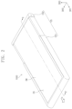
- FIG. 1 is a perspective view of a display apparatus according to one or more embodiments of the present disclosure
- FIG. 2 is a perspective view illustrating an open state of the display apparatus of FIG. 1 according to one or more embodiments of the present disclosure
- FIG. 3 is a perspective view illustrating a display module and a support member according to one or more embodiments of the present disclosure
- FIG. 4 is a cross-sectional view of the display module and the support member cut along the line III-III′ of FIG. 3 according to one or more embodiments of the present disclosure
- FIG. 5 is a cross-sectional view of a display module according to one or more embodiments of the present disclosure.
- FIG. 6 is a cross-sectional view of the display apparatus cut along the line I-I′ of FIG. 1 according to one or more embodiments of the present disclosure
- FIG. 7 is a cross-sectional view of the display apparatus cut along the line II-II′ of FIG. 2 according to one or more embodiments of the present disclosure
- FIG. 8 is a block diagram of a display layer and a display controller according to one or more embodiments of the present disclosure.
- FIG. 9 is a plan view of a display layer according to one or more embodiments of the present disclosure.
- FIGS. 10 A and 10 B are cross-sectional views of a display layer and a sensor layer according to one or more embodiments of the present disclosure
- FIG. 11 is a plan view of a data-driving circuit, a motor, and an AA′ area shown in FIG. 9 , according to one or more embodiments of the present disclosure
- FIG. 12 is a flowchart illustrating driving of a display apparatus according to one or more embodiments of the present disclosure
- FIG. 13 is a plan view of a display layer according to one or more embodiments of the present disclosure.
- FIG. 14 is a cross-sectional view of a portion of a display apparatus according to one or more embodiments of the present disclosure.
- FIG. 15 illustrates a sensor layer and a position-sensing sensor according to one or more embodiments of the present disclosure.
- an implanted region illustrated as a rectangle will, typically, have rounded or curved features and/or a gradient of implant concentration at its edges rather than a binary change from implanted to non-implanted region.
- a buried region formed by implantation may result in some implantation in the region between the buried region and the surface through which the implantation takes place.
- spatially relative terms such as “beneath,” “below,” “lower,” “under,” “above,” “upper,” and the like, may be used herein for ease of explanation to describe one element or feature's relationship to another element(s) or feature(s) as illustrated in the figures. It will be understood that the spatially relative terms are intended to encompass different orientations of the device in use or in operation, in addition to the orientation depicted in the figures. For example, if the device in the figures is turned over, elements described as “below” or “beneath” or “under” other elements or features would then be oriented “above” the other elements or features. Thus, the example terms “below” and “under” can encompass both an orientation of above and below.
- the device may be otherwise oriented (e.g., rotated 90 degrees or at other orientations) and the spatially relative descriptors used herein should be interpreted accordingly.
- first part is described as being arranged “on” a second part, this indicates that the first part is arranged at an upper side or a lower side of the second part without the limitation to the upper side thereof on the basis of the gravity direction.
- the phrase “in a plan view” means when an object portion is viewed from above
- the phrase “in a schematic cross-sectional view” means when a schematic cross-section taken by vertically cutting an object portion is viewed from the side.
- overlap or “overlapped” mean that a first object may be above or below or to a side of a second object, and vice versa. Additionally, the term “overlap” may include layer, stack, face or facing, extending over, covering, or partly covering or any other suitable term as would be appreciated and understood by those of ordinary skill in the art.
- not overlap may include meaning, such as “apart from” or “set aside from” or “offset from” and any other suitable equivalents as would be appreciated and understood by those of ordinary skill in the art.
- face and “facing” may mean that a first object may directly or indirectly oppose a second object. In a case in which a third object intervenes between a first and second object, the first and second objects may be understood as being indirectly opposed to one another, although still facing each other.
- a layer, region, or component when referred to as being “electrically connected” or “electrically coupled” to another layer, region, or component, it can be directly electrically connected or coupled to the other layer, region, and/or component or intervening layers, regions, or components may be present.
- “directly connected/directly coupled,” or “directly on,” refers to one component directly connecting or coupling another component, or being on another component, without an intermediate component.
- a forming direction is not limited to an upper direction but includes forming the portion on a side surface or in a lower direction.
- expressions such as “at least one of,” or “at least one among,” when preceding a list of elements, modify the entire list of elements and do not modify the individual elements of the list.
- “at least one of X, Y, and Z,” “at least one of X, Y, or Z,” and “at least one selected from the group consisting of X, Y, and Z” may be construed as X only, Y only, Z only, any combination of two or more of X, Y, and Z, such as, for instance, XYZ, XYY, YZ, and ZZ, or any variation thereof.
- the expression, such as “at least one of A and B” may include A, B, or A and B.
- “or” generally means “and/or,” and the term “and/or” includes any and all combinations of one or more of the associated listed items.
- the expression, such as “A and/or B” may include A, B, or A and B.
- expressions, such as “at least one of,” “a plurality of,” “one of,” and other prepositional phrases when preceding a list of elements, modify the entire list of elements and do not modify the individual elements of the list.
- first,” “second,” “third,” etc. may be used herein to describe various elements, components, regions, layers and/or sections, these elements, components, regions, layers and/or sections should not be limited by these terms. These terms are used to distinguish one element, component, region, layer or section from another element, component, region, layer or section. Thus, a first element, component, region, layer or section described below could be termed a second element, component, region, layer or section, without departing from the spirit and scope of the present disclosure. The description of an element as a “first” element may not require or imply the presence of a second element or other elements.
- the terms “first,” “second,” etc. may also be used herein to differentiate different categories or sets of elements. For conciseness, the terms “first,” “second,” etc. may represent “first-category (or first-set),” “second-category (or second-set),” etc., respectively.
- the x-axis, the y-axis, and/or the z-axis are not limited to three axes of a rectangular coordinate system, and may be interpreted in a broader sense.
- the x-axis, the y-axis, and the z-axis may be perpendicular to one another, or may represent different directions that are not perpendicular to one another. The same applies for first, second, and/or third directions.
- a specific process order may be performed differently from the described order.
- two consecutively described processes may be performed substantially at the same time or performed in an order opposite to the described order.
- the term “substantially,” “about,” “approximately,” and similar terms are used as terms of approximation and not as terms of degree, and are intended to account for the inherent deviations in measured or calculated values that would be recognized by those of ordinary skill in the art. “About” or “approximately,” as used herein, is inclusive of the stated value and means within an acceptable range of deviation for the particular value as determined by one of ordinary skill in the art, considering the measurement in question and the error associated with measurement of the particular quantity (i.e., the limitations of the measurement system). For example, “about” may mean within one or more standard deviations, or within ⁇ 30%, 20%, 10%, 5% of the stated value. Further, the use of “may” when describing embodiments of the present disclosure refers to “one or more embodiments of the present disclosure.”
- block, unit, and/or module are/is physically implemented by a logic circuit, an individual component, a microprocessor, a hard wire circuit, a memory element, a line connection, and other electronic circuits. This may be formed using a semiconductor-based manufacturing technique or other manufacturing techniques.
- the block, unit, and/or module implemented by a microprocessor or other similar hardware may be programmed and controlled using software to perform various functions discussed herein, optionally may be driven by firmware and/or software.
- each block, unit, and/or module may be implemented by dedicated hardware, or a combination of dedicated hardware that performs some functions and a processor (for example, one or more programmed microprocessors and related circuits) that performs a function different from those of the dedicated hardware.
- the block, unit, and/or module may be physically separated into two or more interact individual blocks, units, and/or modules without departing from the scope of the present disclosure.
- the block, unit and/or module may be physically combined into more complex blocks, units, and/or modules without departing from the scope of the present disclosure.
- FIG. 1 is a perspective view of a display apparatus according to one or more embodiments of the present disclosure
- FIG. 2 is a perspective view of an open state of the display apparatus according to one or more embodiments of the present disclosure.
- the display apparatus 1000 may include a display module DM, and a case CS in which the display module DM is accommodated.
- the display module DM may be exposed to the outside through an opening defined on the top of the case CS.
- the case CS may include a first case CS 1 and a second case CS 2 .
- the first case CS 1 and the second case CS 2 may be coupled to each other to accommodate the display module DM.
- the first case CS 1 may be coupled to the second case CS 2 in such a way that the first case CS 1 is movable in a first direction DR 1 .
- FIG. 1 shows a closed state of the display apparatus 1000 before the first case CS 1 moves.
- a direction crossing the first direction DR 1 is defined as a second direction DR 2 .
- a direction substantially perpendicularly crossing a plane defined by the first and second directions DR 1 and DR 2 is defined as a third direction DR 3 .
- the components may be viewed in a direction opposite to the third direction DR 3 .
- a display surface DS may be defined to be exposed through the opening of the case CS.
- the area of the display surface DS may be adjusted by movement of the first case CS 1 with respect to the second case CS 2 .
- the display module DM may be a flexible display module, and may be supported by a support member located under the display module DM.
- the support member may be connected to the first case CS 1 , and when the first case CS 1 moves in the first direction DR 1 , the support member may also move in the first direction DR 1 .
- FIG. 2 illustrates an open state in which the first case CS 1 of the display apparatus 1000 moves in the first direction DR 1 .
- a portion of the display module DM that is not exposed to the outside may be located in the first case CS 1 .
- the size of the display surface DS may increase in the first direction DR 1 by the movement of the first case CS 1 .
- the display module DM located on the support member moves together with the support member in the first direction DR 1 , which results in expansion of the display surface DS of the display module DM. Accordingly, the user may view the image through the expanded screen.
- a state of the display apparatus 1000 in which the display surface DS of the display module DM is set as a default size may be defined as a closed state.
- a state of the display apparatus 1000 in which the display surface DS of the display module DM expands may be defined as an open state.
- the closed state of the display apparatus 1000 may correspond to the closed state of the case CS
- the open state of the display apparatus 1000 may correspond to the open state of the case CS.
- the case CS 1 moves in the first direction DR 1 to expand the display DS of the display module DM and the case CS may be changed to the open state.
- the case CS may change the display apparatus 1000 from the closed state to the open state, and vice versa.
- FIG. 3 a perspective view showing a display module and a support member according to one or more embodiments of the present disclosure
- FIG. 4 is a cross-sectional view of the display module and the support member cut along the line III-III′ of FIG. 3 according to one or more embodiments of the present disclosure.
- the display module DM may include a display layer 100 and a sensor layer 200 .
- the display layer 100 may be a component configured to substantially generate an image.
- the display layer 100 may be an emissive display layer, but is not particularly limited thereto.
- the display layer 100 may be an organic light-emitting-display layer, a quantum dot light-emitting-display layer, a micro-LED-display layer, or a nano-LED-display layer.
- a light-emitting layer of the organic light-emitting-display layer may include an organic light-emitting material.
- a light-emitting layer of the quantum dot light-emitting display panel may include quantum dots, quantum rods, or the like.
- a light emission layer of the micro-LED-display layer may include micro-LEDs.
- a light emission layer of the nano-LED-display layer may include nano-LEDs.
- the sensor layer 200 may be located on the display layer 100 .
- the sensor layer 200 may sense an external input.
- the display surface DS of the display module DM may include a first area AA 1 and a second area AA 2 .
- the first area AA 1 may be provided in a size corresponding to the display surface DS in FIG. 1 to determine the size of the screen in the closed state.
- the first area AA 1 may be exposed to the outside in the closed state and in the open state.
- the display surface DS may be defined as the first area AA 1 in the closed state while the second area AA 2 is not exposed to the outside.
- a portion of the first area AA 1 and the second area AA 2 may be exposed to the outside in the closed state.
- the second area AA 2 may expand or extend in the first direction DR 1 from the first area AA 1 .
- the second AA 2 may be adjacent to the first area AA 1 .
- the screen size of the display apparatus 1000 may increase by at least the area of the exposed portion of the second area AA 2 .
- another portion other than at least the exposed portion of the second AA 2 , might not be exposed to the outside.
- the other portion might not be exposed to the outside in the closed and open states.
- the support member SP may be located under the display module DM to support the display module DM.
- the support member SP may be located at the rear surface opposite to the display surface DS of the display module DM.
- the support member SP may be composed of a material with higher rigidity than the display module DM.
- the support member SP may be a metal plate, such as aluminum.
- the support member SP may include a first support part SP 1 , a plurality of support bars SB, and a second support part SP 2 .
- the first support part SP 1 may support the first area AA 1 of the display module DM
- the plurality of support bars SB and the second support part SP 2 may support the second area AA 2 of the display module DM.
- the plurality of support bars SB may be located between the first support part SP 1 and the second support part SP 2 . Each of the plurality of support bars SB may extend in the second direction DR 2 . The plurality of support bars SB may be arranged to be spaced apart from each other in the first direction DR 1 . In one or more embodiments of the present disclosure, when viewed in the second direction DR 2 , each of the plurality of support bars SB may have a reversed trapezoidal shape on the basis of the display surface DS of the display module DM. Due to the shapes, the plurality of support bars SB may be suitably bent.
- the plurality of support bars SB spaced apart from each other in the first direction DR 1 are shown as an example, but the structure of the plurality of support bars SB is not limited thereto.
- the plurality of support bars SB may have a joint structure in which the support bars SB are combined to rotate around each other.
- the first support part SP 1 may have a plane defined by the first and second directions DR 1 and DR 2 .
- the first support part SP 1 may be provided in a size corresponding to the first area AA 1 of the display module DM.
- the first support part SP 1 may be located at the rear surface opposite to the display surface DS of the display module DM to support the first area AA 1 of the display module DM.
- a second support part SP 2 may overlap the second area AA 2 . At least a portion of the second support part SP 2 may face, or may be opposite to, the first support part SP 1 in the closed state. Description thereabout will be provided below.
- the second support part SP 2 may include a metal plate.
- the plurality of support bars SB and the second support part SP 2 may be located at the rear surface of the display module DM to support the second area AA 2 .
- an adhesive may be located between the display module DM and the support member SP to attach the support member SP to the rear surface of the display module DM.
- the adhesive may include a pressure sensitive adhesive, or may include various other adhesives without being limited thereto.
- FIG. 5 is a cross-sectional view of a display module according to one or more embodiments of the present disclosure.
- the display module DM may include a display layer 100 and a sensor layer 200 .
- the display layer 100 may include a base layer 110 , a circuit layer 120 , a light-emitting-element layer 130 , and an encapsulation layer 140 .
- the base layer 110 may be a member for providing a base surface with the circuit layer 120 located thereon.
- the base layer 110 may be a glass substrate, a metal substrate, or a polymer substrate.
- the present disclosure is not limited thereto, and the base layer 110 may be an inorganic layer, an organic layer, or a composite material layer.
- the base layer 110 may have a multilayer structure.
- the base layer 110 may include a first composite resin layer, a silicon oxide (SiOx) layer located on the composite resin layer, an amorphous silicon (a-Si) layer located on the silicon oxide layer, and a second composite resin layer located on the amorphous silicon layer.
- the silicon oxide layer and the amorphous silicon layer may be referred to as a base barrier layer.
- Each of the first and second composite resin layers may include polyimide-based resin.
- each of the first and second composite resin layers may include at least one among an acrylate-based resin, a methacrylate-based resin, a polyisoprene-based resin, a vinyl-based resin, an epoxy-based resin, a urethane-based resin, a cellulose-based resin, a siloxane-based resin, a polyamide-based resin, or a perylene-based resin.
- ⁇ ⁇ ”-based resin means including a functional group “ ⁇ ⁇ ”.
- the circuit layer 120 may be located on the base layer 110 .
- the circuit layer 120 may include an insulation layer, a semiconductor pattern, a conductive pattern, a signal line and the like.
- the insulation layer, the semiconductor layer, and the conductive layer are defined on the base layer 110 in a manner of coating, deposition, or the like, and then the insulation layer, the semiconductor layer, and the conductive layer may be selectively patterned through a plurality of times of a photolithography process. Then, the semiconductor pattern, the conductive pattern, and the signal line included in the circuit layer 120 may be provided.
- the light-emitting-element layer 130 may be located on the circuit layer 120 .
- the light-emitting-element layer 130 may include a light-emitting element.
- the light-emitting-element layer 130 may include an organic light-emitting material, a quantum dot, a quantum rod, a micro-LED, or a nano-LED.
- the encapsulation layer 140 may be located on the light-emitting-element layer 130 .
- the encapsulation layer 140 may protect the light-emitting-element layer 130 from a foreign matter, such as moisture, oxygen, and dust particles.
- the sensor layer 200 may be located on the display layer 100 .
- the sensor layer 200 may sense an external input applied from the outside.
- the sensor layer 200 may be located on the display layer 100 through continuous processes.
- the sensor layer 200 may be represented as being directly located on the display layer 100 . Being “directly located on” may mean that a third element is not located between the sensor layer 200 and the display layer 100 .
- a separate adhesive member might not be located between the sensor layer 200 and the display layer 100 .
- the sensor layer 200 may be bonded to the display layer 100 through an adhesive member.
- the adhesive member may include a typical adhesive or a pressure sensitive adhesive.
- FIG. 6 is a cross-sectional view of the display apparatus cut along the line I-I′ of FIG. 1 according to one or more embodiments of the present disclosure
- FIG. 7 is a cross-sectional view of the display apparatus cut along the line II-II′ of FIG. 2 according to one or more embodiments of the present disclosure.
- the display apparatus 1000 may include a display module DM, a support member SP, and a case CS.
- the display apparatus 1000 may have a closed state and an open state.
- the closed state and open state of the display apparatus 1000 may be determined according to a sliding operation of the case CS.
- the closed state of the display apparatus 10000 in one or more embodiments of the present disclosure may correspond to a case where the first case CS 1 and the second case CS 2 move to the end in a direction as they get closer to each other.
- the open state of the display apparatus 1000 may correspond to a case where the first case CS 1 and the second case CS 2 move to the end in a direction as they get away from each other.
- the closed state and open state of the display apparatus 1000 may be determined on the basis of an area exposed to the outside.
- a first area AA 1 and a second area AA 2 may be defined in the display module DM.
- the first area AA 1 may be exposed to the outside in the closed state.
- the second area AA 2 may expand or extend from the first area AA 1 .
- the second area AA 2 might not be exposed to the outside in the closed state.
- the second area AA 2 may include a curvature area CA having a curvature, and a flat area FA expanding from the curvature area CA and facing, or opposite to, the first area AA 1 .
- at least a portion of the second area AA 2 may be exposed to the outside in the open state.
- At least the portion of the second area AA 2 may be defined as a first portion AAP 1 .
- a portion of the second area AA 2 which is not exposed to the outside (e.g., in a closed state), may be defined as a second portion AAP 2 .
- At least a portion of the second area AA 2 which is exposed to the outside in the open state, may be located in the curvature area CA in the closed state.
- the support member SP may support the display module DM.
- the support member SP may include a first support part SP 1 and a second support part SP 2 .
- the support member SP may include a metal plate.
- the first support part SP 1 may support the first area AA 1 of the display module DM
- the second support part SP 2 may support the flat area FA in the second area AA 2 of the display module DM.
- the second support part SP 2 which supports the flat area FA, may include a metal plate.
- the support member SP may include the plurality of support bars SB.
- the plurality of support bars SB may support the curvature area CA in the second area AA 2 .
- the support member SP may further include a sub-support plate SSP.
- the sub-support plate SSP may be located at the rear surface of the first support part SP 1 to support the first support part SP 1 .
- an accommodation space which may accommodate various kinds of components (such as a battery or a driving element), may be provided between the sub-support plate SSP and the first bottom part BP 1 .
- the case CS may accommodate the display module DM and the support member SP.
- the case CS may include a first case CS 1 and a second case CS 2 .
- the second case CS 2 may be coupled to the first case CS 1 so as to move closer to, or further away from, the first case CS 1 in the first direction DR 1 .
- the display module DM and the support member SP may be fixed and coupled to the first case CS 1 .
- the case CS may switch between the closed state and the open state of the display apparatus 1000 by means of a sliding operation.
- the first case CS 1 may include a side wall OSW and a first bottom part BP 1 .
- the second case CS 2 may include a side wall SW and a second bottom part BP 2 .
- the display module DM and the support member SP may be fixed to the side wall OSW of the first case CS 1 .
- the display apparatus 1000 may include a rotation unit RU.
- the rotation unit RU may be located in, and coupled to, the second case CS 2 .
- the rotation unit RU may be coupled to the side wall SW of the second case CS 2 .
- the rotation unit RU may rotate according to the sliding operation of the case CS, and may expand or contract the display surface DS (see FIG. 1 ).
- FIG. 8 is a block diagram of a display layer and a display controller (e.g., display control unit) according to one or more embodiments of the present disclosure.
- a display controller e.g., display control unit
- the display layer 100 may include a plurality of scan lines SL 1 to SLn, a plurality of data lines DL 1 to DLM, and a plurality of pixels PX.
- the plurality of pixels PX may be respectively connected to corresponding data lines among the plurality of data lines DL 1 to DLm, and to corresponding scan lines among the plurality of scan lines SL 1 to SLm.
- the display layer 100 may further include light emission control lines, and the display controller 100 C may also further include a light-emission-driving circuit configured to provide control signals to the light emission control lines, Description thereabout will be provided below.
- the configuration of the display layer 100 is not particularly limited.
- the display controller 100 C may include a signal control circuit 100 C 1 , a scan-driving circuit 100 C 2 , and a data-driving circuit 100 C 3 .
- the signal control circuit 100 C 1 may receive input data RGB and a control signal D-CS from an external controller (e.g., external control unit).
- the external controller may include a graphic processor (e.g., a graphic processing unit).
- the control signal D-CS may include various signals.
- the control signal D-CS may include an input vertical synchronization signal, an input horizontal synchronization signal, a main clock, a data enable signal and the like.
- the signal control circuit 100 C 1 may generate a first control signal CONT 1 and a vertical synchronization signal Vsync on the basis of (e.g., based on) the control signal D-CS, and may output the first control signal CONT 1 and the vertical synchronization signal Vsync to the scan-driving circuit 100 C 2 .
- the vertical synchronization signal Vsync may be included in the first control signal CONT 1 .
- the signal control circuit 100 C 1 may generate a second control signal CONT 2 and a horizontal synchronization signal Hsync on the basis of the control signal D-CS, and may output the second control signal CONT 2 and the horizontal synchronization signal Hsync to the data-driving circuit 100 C 3 .
- the horizontal synchronization signal Hsync may be included in the second control signal CONT 2 .
- the signal control circuit 100 C 1 may output a data signal DTS to the data-driving circuit 100 C 3 , the data signal being obtained by processing the image data RGB in correspondence to an operation condition of the display layer 100 .
- the first control signal CONT 1 and the second control signal CONT 2 are respective signals suitable for operating the scan-driving circuit 100 C 2 and the data-driving circuit 100 C 3 , and are not particularly limited.
- the scan-driving circuit 100 C 2 may drive the plurality of scan lines SL 1 to SLn in response to the first control signal CONT 1 and the vertical synchronization signal Vsync.
- the scan-driving circuit 100 C 2 may be provided in the same process as the circuit layer 120 (see FIG. within the display layer 100 , but is not limited thereto.
- the scan-driving circuit 100 C 2 may be implemented in an integrated circuit to be directly mounted in a prescribed area of the display layer 100 , or may be mounted on a separate printed circuit board in a chip on film (COF) manner to be electrically connected to the display layer 100 .
- COF chip on film
- the data-driving circuit 100 C 3 may output grayscale voltages for driving the plurality of data lines DL 1 to DLm in response to the second control signal CONT 2 , the horizontal synchronization signal Hsync, and the data signal DTS from the signal control circuit 100 C 1 .
- the data-driving circuit 100 C 3 may be implemented in an integrated circuit to be directly mounted in a prescribed area of the display layer 100 , or may be mounted on a separate printed circuit board in the COF manner to be electrically connected to the display layer 100 , but is not particularly limited.
- the data-driving circuit 100 C 3 may be provided in the same process as the circuit layer 120 (see FIG. 2 A ) within the display layer 100 .
- FIG. 9 is a plan view of a display layer according to one or more embodiments of the present disclosure.
- the display layer 100 may include a base layer 110 , the plurality of pixels PX, the plurality of signal lines SL 1 to SLm, DL 1 to DLn, EL 1 to ELm, CSL 1 , CSL 2 , PL, and CNL electrically connected to the pixels PX, the scan-driving circuit 100 C 2 , the data-driving circuit 100 C 3 , an emission-driving circuit EDV, a plurality of deformation sensors (e.g., deformation-sensing units) SGS, and a plurality of deformation sensor drivers (e.g., deformation-driving units or deformation-sensing-driving units) SGD.
- the data-driving circuit 100 C 3 may be referred to as a driving circuit 100 C 3 .
- Each of the plurality of pixels may include a pixel-driving circuit composed of a light-emitting element, a plurality of transistors (e.g., switching transistors, driving transistors or the like) connected to the light-emitting element, and at least one capacitor.
- a pixel-driving circuit composed of a light-emitting element, a plurality of transistors (e.g., switching transistors, driving transistors or the like) connected to the light-emitting element, and at least one capacitor.
- the pixels PX may be located in a display area DA. Each of the pixels PX may emit light in correspondence to an electrical signal applied thereto. However, some of the pixels PX may include a thin-film transistor located in a non-display area NDA, and is not limited to any one embodiment.
- the scan-driving circuit 100 C 2 , the data-driving circuit 100 C 3 , and the emission-driving circuit EDV may be located in the non-display area NDA.
- the present disclosure is not limited thereto, and at least one among the scan-driving circuit 100 C 2 , the data-driving circuit 100 C 3 , or the emission-driving circuit EDV may be located in the display area DA, thereby reducing the area of the non-display area NDA.
- the data-driving circuit 100 C 3 may be provided in a type of an integrated circuit chip defined as a driving chip to be mounted in the non-display area NDA of the display layer 100 .
- the present disclosure is not limited thereto, and the data-driving circuit 100 C 3 may be mounted on a separate flexible circuit board connected to the display layer 100 to be electrically connected to the display layer 100 .
- the signal lines SL 1 to SLm, DL 1 to DLn, EL 1 to ELm, CSL 1 , CSL 2 , PL, and CNL may include the scan lines DL 1 to DLn, the data lines DL 1 to DLn, emission lines EL 1 to ELm, first and second controls lines CSL 1 and CSL 2 , a power line PL, and connection lines CNL.
- m and n are natural numbers.
- the data lines DL 1 to DLn may be insulated from, and may cross, the signal lines SL 1 to SLm and the emission lines EL 1 to ELm.
- the scan lines SL 1 to SLm may extend in the second direction DR 2 to be connected to the scan-driving circuit 100 C 2 .
- the data lines DL 1 to DLn may extend in the first direction DR 1 to be connected to the data-driving circuit 100 C 3 .
- the emission lines EL 1 to ELm may extend in the second direction DR 2 to be connected to the emission-driving circuit EDV.
- the power line PL may extend in the first direction DR 1 to be located in the non-display area NDA. In one or more embodiments, the power line PL may be located between the display area DA and the emission-driving circuit EDV. However, the location and arrangement of the power line PL is not limited thereto.
- connection lines CNL may extend in the second direction DR 2 , and may be arranged in the first direction DR 1 to be connected to the power line PL and the pixels PX.
- the connection lines CNL may be located on different respective layers from the power line PL, and may be electrically connected through a contact hole.
- the present disclosure is not limited thereto, and the connection lines CNL may be integrated with the power line PL on the same layer.
- the power supply voltage may be applied to the pixels PX through the power line PL and the connection lines CNL that are connected to each other.
- the first control line CSL 1 may be connected to the scan-driving circuit 100 C 2 .
- the second control line CSL 2 may be connected to the emission-driving circuit EDV.
- the pads PD may be located adjacent to the lower end of the non-display area NDA.
- the pads PD may be more adjacent to the lower end of the display layer 100 than the data-driving circuit 100 C 3 .
- the pads PD may be spaced apart from each other in the second direction DR 2 .
- the pads PD may be portions to which a circuit board is connected, the circuit board being configured to provide a signal for controlling the operations of the scan-driving circuit 100 C 2 , the data-driving circuit 100 C 3 , and the emission-driving circuit EDV of the display layer 100 .
- the pads PD may be connected to respectively corresponding signal lines among the signal lines.
- the power line PL and the first and second control lines CSL 1 and CSL 2 may be connected to the pads PD.
- the data lines DL 1 to DLn may be electrically connected to the corresponding pads PD through the data-driving circuit 100 C 3 .
- the scan-driving circuit 100 C 2 may generate scan signals in response to the scan control signal.
- the scan signals may be applied to the pixels PX through the scan lines SL 1 to SLm.
- the data-driving circuit 100 C 3 may generate data voltages corresponding to the image signals in response to the data control signal.
- the data voltages may be applied to the pixels through the data lines DL 1 to DLn.
- the emission-driving circuit EDV may generate emission signals in response to the emission control signal.
- the emission signals may be applied to the pixels PX through the emission lines EL 1 to ELm.
- the pixels PX may receive the data voltages in response to the scan signals.
- the pixels PX may display an image by emitting light of respective brightness levels corresponding to the data voltages in response to the emission signals.
- An emission time of the pixels PX may be controlled by the emission signals. Accordingly, the display layer 100 may output an image through the display area DA by the pixels PX.
- the plurality of deformation sensors SGS may be adjacent to the display area DA, and may be located in the non-display area NDA.
- the plurality of deformation sensors SGS may be arranged in the first direction DR 1 .
- the plurality of deformation sensors SGS may be located in the second area AA 2 . In other words, when viewed in a plan view, the plurality of deformation sensors SGS might not overlap the first area AA 1 , and may overlap the second area AA 2 . In a plan view, the plurality of deformation sensors SGS may overlap the plurality of support bars SB (see FIG. 6 ) and the second support part SP 2 (see FIG. 6 ). In a plan view, the plurality of deformation sensors SGS might not overlap the first support part SP 1 (see FIG. 6 ). The plurality of deformation sensors SGS may be spaced apart from each other with the display area DA interposed therebetween.
- Each of the plurality of deformation sensors SGS may have a change in resistance value in correspondence to the shape of the display layer 100 .
- the plurality of deformation sensors SGS may be electrically connected to the data-driving circuit 100 C 3 .
- Each of the plurality of deformation sensors SGS may be electrically connected in the first direction DR 1 .
- the plurality of deformation sensor drivers SGD may be adjacent to the display area DA, and may be located in the non-display area NDA.
- the plurality of deformation sensor drivers SGD may be arranged in the first direction DR 1 .
- the plurality of deformation sensor drivers SGD may be spaced apart from the plurality of deformation sensors SGS in the second direction DR 2 .
- the plurality of deformation sensor drivers SGD may be located in the second area AA 2 . When viewed in a plan view, the plurality of deformation sensor drivers SGD may not overlap the first area AA 1 , and may overlap the second area AA 2 . When viewed in a plan view, the plurality of deformation sensor drivers SGD may overlap the plurality of support bars SB (see FIG. 6 ) and the second support part SP 2 (see FIG. 6 ). When viewed in a plan view, the plurality of deformation sensor drivers SGD might not overlap the first support part SP 1 (see FIG. 6 ). The plurality of deformation sensor drivers SGD may be spaced apart from each other with the display area DA interposed therebetween.
- the plurality of deformation sensor drivers SGD may be respectively connected to the plurality of deformation sensors SGS. Each of the plurality of deformation sensor drivers SGD may be electrically connected in the first direction DR 1 . The plurality of deformation sensor drivers SGD may be electrically connected to the data-driving circuit 100 C 3 .
- the scan-driving circuit 100 C 2 , the display area DA, the emission-driving circuit EDV, the plurality of deformation sensor drivers SGD, and the plurality of deformation sensors SGS may be sequentially arranged in the second direction DR 2 .
- the plurality of deformation sensors SGS may be located in the outermost region of the display layer 100 .
- the plurality of deformation sensor drivers SGD may sequentially drive the plurality of deformation sensors SGS in the first direction DR 1 , and on the basis thereof, the data-driving circuit 100 C 3 may sequentially measure the resistance values of the plurality of deformation sensors SGS.
- the data-driving circuit 100 C 3 may understand the sliding position of the display layer 100 on the basis of the resistance values.
- the display apparatus 1000 (see FIG. 1 ) may control whether to display an image to be displayed on the second area AA 2 on the basis of the sliding position. Therefore, the display apparatus 1000 (see FIG. 1 ) with improved power efficiency may be provided. Accordingly, the display apparatus 1000 (see FIG. 1 ) with improved reliability may be provided.
- FIG. 10 A is a cross-sectional view of a display layer and a sensor layer according to one or more embodiments of the present disclosure.
- like reference numerals are given to the elements described with reference to FIG. 5 , and a repeated description thereabout will be omitted.
- At least one inorganic layer may be provided on the top surface of the base layer 110 .
- the inorganic layer may include at least any one among aluminum oxide, titanium oxide, silicon oxide, silicon oxynitride, zirconium oxide, or hafnium oxide.
- the inorganic layer may be provided with multilayer.
- the multilayered inorganic layer may compose a barrier layer and/or a buffer layer.
- the display layer 100 is illustrated to include the buffer layer BFL.
- the buffer layer BFL may enhance the bonding force between the base layer 110 and the semiconductor pattern.
- the buffer layer BFL may include silicon oxide layers and silicon nitride layers that may be alternately laminated.
- the semiconductor pattern may be located on the buffer layer BFL.
- the semiconductor pattern may include polysilicon.
- the present disclosure is not limited thereto, and the semiconductor pattern may also include amorphous silicon, low-temperature polycrystalline silicon, or oxide semiconductor.
- FIG. 10 A only illustrates a portion of the semiconductor pattern, and the remaining portion(s) of the semiconductor pattern may be further located in another area.
- the semiconductor pattern may be arranged in a specific rule across the pixels.
- the semiconductor pattern has different electrical properties according to whether to be doped or not.
- the semiconductor pattern may include a first area having high conductivity and a second area having low conductivity.
- the first area may be doped with an N-type dopant or a P-type dopant.
- a P-type transistor includes a doped area doped with a P-type dopant, and an N-type transistor includes a doped area doped with an N-type dopant.
- the second area may be a non-doped area, or may be doped at a low concentration in comparison to the first area.
- the first area may have a greater conductivity than the second area, and may substantially operate as an electrode or a signal line.
- the second area may substantially correspond to an active area (or a channel) of a transistor.
- a portion of the semiconductor pattern may be an active area of the transistor, another portion may be a source or a drain, and another portion may be a connection electrode or a signal connection line.
- Each of the pixels may have an equivalent circuit including seven transistors, one capacitor, and a light-emitting element, and the equivalent circuit of the pixel may be deformed in various types.
- FIG. 10 A one transistor 100 PC and a light-emitting element 100 PE included in a pixel are illustrated as an example.
- the transistor 100 PC may include a source SC 1 , an active area A 1 , a drain D 1 , and a gate G 1 .
- the source SC 1 , the active are A 1
- the drain D 1 may be provided from the semiconductor pattern.
- the source SC 1 and the drain D 1 may extend from the active area A 1 on a cross section in opposite directions from each other.
- FIG. 5 illustrates a portion of the signal connection line SCL provided from the semiconductor pattern.
- the signal connection line SCL may be electrically connected to the drain D 1 of the transistor 100 PC on a plane.
- the first insulation layer 10 may be located on the buffer layer BFL.
- the first insulation layer 10 may commonly overlap the plurality of pixels and may cover the semiconductor pattern.
- the first insulation layer 10 may be an inorganic layer and/or an organic layer, and may have a single-layer structure or multilayer structure.
- the first insulation layer 10 may include at least any one among aluminum oxide, titanium oxide, silicon oxide, silicon nitride, silicon oxynitride, zirconium oxide, or hafnium oxide.
- the first insulation layer 10 may be a silicon oxide layer of a single layer.
- the insulation layer of the circuit layer 120 which will be described below, may be an inorganic layer and/or an organic layer, and may have a single-layer structure or multilayer structure.
- the inorganic layer may include at least one among the foregoing materials, but is not limited thereto.
- the gate G 1 may be located on the first insulation layer 10 .
- the gate G 1 may be a portion of a metal pattern.
- the gate G 1 may overlap the active area A 1 .
- the gate G 1 may function as a mask in a process of doping the semiconductor pattern.
- the second insulation layer 20 may be located on the first insulation layer 10 and may cover the gate G 1 .
- the second insulation layer 20 may commonly overlap the pixels.
- the second insulation layer 20 may be an inorganic layer and/or an organic layer, and may have a single-layer structure or multilayer structure.
- the second insulation layer 20 may include any one among silicon oxide, silicon nitride, or silicon oxynitride.
- the second insulation layer 20 may have a multilayer structure including a silicon oxide layer and a silicon nitride layer.
- a third insulation layer 30 may be located on the second insulation layer 20 .
- the third insulation layer 30 may have a single-layer structure or multilayer structure.
- the third insulation layer 30 may have a multilayer structure including a silicon oxide layer and a silicon nitride layer.
- a first connection electrode CNE 1 may be located on the third insulation layer 30 .
- the first connection electrode CNE 1 may be connected to the signal connection line SCL through a contact hole CNT- 1 penetrating through the first to third insulation layers 10 , 20 , and 30 .
- a fourth insulation layer 40 may be located on the third insulation layer 30 .
- the fourth insulation layer 40 may be silicon oxide layer of a single layer.
- a fifth insulation layer 50 may be located on the fourth insulation layer 40 .
- the fifth insulation layer 50 may be an organic layer.
- a second connection electrode CNE 2 may be located on the fifth insulation layer 50 .
- the second connection electrode CNE 2 may be connected to the first connection electrode CNE 1 through a contact hole CNT- 2 penetrating through the fourth insulation layer 40 and the fifth insulation layer 50 .
- a sixth insulation layer 60 may be located on the fifth insulation layer 50 and may cover the second connection electrode CNE 2 .
- the sixth insulation layer 60 may be an organic layer.
- the light-emitting-element layer 130 may be located on the circuit layer 120 .
- the light-emitting-element layer 130 may include a light-emitting element 100 PE.
- the light-emitting-element layer 130 may include an organic light-emitting material, a quantum dot, a quantum rod, a micro-LED, or a nano-LED.
- the light-emitting element 100 PE is described as, for example, an organic light-emitting element, but is not limited thereto.
- the light-emitting element 100 PE may include a first electrode AE, a light-emitting layer EL, and a second electrode CE.
- the first electrode AE may be located on a sixth insulation layer 60 .
- the first electrode AE is connected to the second connection electrode CNE 2 through a contact hole CNT- 3 penetrating through the sixth insulation layer 60 .
- a pixel definition layer 70 may be located on the sixth insulation layer 60 and may cover a portion of the first electrode AE.
- the pixel definition layer 70 is defined with an opening 70 -OP.
- the opening 70 -OP of the pixel definition layer 70 exposes at least a portion of the first electrode AE.
- the display area DA may include a light-emitting area PXA, and a non-light-emitting area NPXA adjacent to the light-emitting area PXA.
- the non-light-emitting area NPXA may surround the light-emitting area PXA.
- the light-emitting area PXA is defined in correspondence to a partial area of the first electrode AE exposed by the opening 70 -OP.
- the light-emitting layer EL may be located on the first electrode AE.
- the light-emitting layer EL may be located on an area corresponding to the opening 70 -OP.
- the light-emitting layer EL may be separately provided in each of the plurality of pixels.
- each of the separately provided light-emitting layers EL may emit light of one color among blue, red, and green.
- the present disclosure is not limited thereto, and the light-emitting layers EL may be connected and commonly provided to the pixels. In this case, the light-emitting layer EL may provide blue light, or may provide white light.
- the second electrode CE may be located on the light-emitting layer EL.
- the second electrode CE may have an integrated shape, and may be commonly located in the plurality of pixels.
- a hole control layer may be located between the first electrode AE and the light-emitting layer EL.
- the hole control layer may be commonly located on the light-emitting area PXA and the non-light-emitting area NPXA.
- the hole control layer may include a hole transport layer, and may further include a hole injection layer.
- An electron control layer may be located between the light-emitting layer EL and the second electrode CE.
- the electron control layer may include an electron transport layer, and may further include an electron injection layer.
- the hole control layer and the electron control layer may be commonly provided in the plurality of pixels using an open mask.
- the encapsulation layer 140 may be located on the light-emitting-element layer 130 .
- the encapsulation layer 140 may include an inorganic layer, an organic layer, and an inorganic layer that are sequentially laminated, but the layers defining the encapsulation layer 140 are not limited thereto.
- the inorganic layers may protect the light-emitting-element layer 130 from moisture and oxygen, and the organic layer may protect the light-emitting-element layer 130 from a foreign matter, such as dust particles.
- the inorganic layers may include a silicon nitride layer, a silicon oxynitride layer, a silicon oxide layer, a titanium oxide layer, or an aluminum oxide layer.
- the organic layer may include an acrylic-based organic layer, but is not limited thereto.
- the sensor layer 200 may be located on the display layer 100 through continuous processes. In this case, the sensor layer 200 may be directly located on the display layer 100 , meaning that a third element is not located between the sensor layer 200 and the display layer 100 . In other words, a separate adhesive member might not be located between the sensor layer 200 and the display layer 100 . Alternatively, the sensor layer 200 may be adhered to the display layer 100 through an adhesive member.
- the adhesive member may include a typical adhesive or a pressure sensitive adhesive.
- the sensor layer 200 may include a base insulation layer 201 , a first conductive layer 202 , a sensing insulation layer 203 , a second conductive layer 204 , and a cover insulation layer 205 .
- the base insulation layer 201 may be an inorganic layer including any one among silicon nitride, silicon oxynitride, and silicon oxide. Alternatively, the base insulation layer 201 may be an organic layer including an epoxy resin, an acrylic resin, or an imide-based resin. The base insulation layer 201 may have a single-layer structure, or a multilayer structure laminated along the third direction DR 3 .
- Each of the first conductive layer 202 and the second conductive layer 204 may have a single-layer structure or a multilayer structure laminated along the third direction DR 3 .
- the first conductive layer 202 and the second conductive layer 204 may provide a sensing electrode configured to sense an external input.
- the conductive layer of the single layer structure may include a metal layer or a transparent conductive layer.
- the metal layer may include molybdenum, silver, titanium, copper, aluminum, or an alloy thereof.
- the transparent conductive layer may include a transparent conductive oxide, such as indium tin oxide (ITO), indium zinc oxide (IZO), zinc oxide (ZnO), indium zinc tin oxide (IZTO) or the like.
- the transparent conductive layer may include a conductive polymer, such as PEDOT, a metal nanowire, or graphene.
- the conductive layer of a multilayer structure may include metal layers.
- the layers may have a three-layer structure of titanium/aluminum/titanium.
- the conductive layer of the multilayer structure may include at least one metal layer and at least one transparent conductive layer.
- At least one of the sensing insulation layer 203 and the cover insulation layer 205 may include an inorganic film.
- the inorganic film may include at least any one among aluminum oxide, titanium oxide, silicon oxide, silicon oxynitride, zirconium oxide or hafnium oxide.
- At least one of the sensing insulation layer 203 and the cover insulation layer 205 may include an organic film.
- the organic film may include at least one among an acrylic-based resin, a meta-acrylic-based resin, polyisoprene, a vinyl-based resin, an epoxy-based resin, a urethane-based resin, a cellulose-based resin, a siloxane-based resin, a polyimide based-resin, a polyamide-resin, and a parylene-based resin.
- the deformation sensor SGSa and the deformation sensor driver SGDa may be located on the buffer layer BFL.
- the deformation sensor SGSa and the deformation sensor driver SGDa may be provided on the same layer as the transistor 100 PC.
- the deformation sensor SGSa and the deformation sensor driver SGDa may be located on the same layer as the source SC 1 , the active area A 1 , and the drain D 1 .
- the arrangement relationship between the deformation sensors SGSa and the deformation sensor driver SGDa according to one or more embodiments of the present disclosure is not limited thereto.
- the deformation sensor SGSa and the deformation sensor driver SGDa may be located on the same layer as the gate G 1 .
- the deformation sensor SGSa and the deformation sensor driver SGDa may be provided in the same layer as the display layer 100 .
- the deformation sensor drivers SGDa may sequentially drive the deformation sensor SGSa in the first direction DR 1 , and on the basis thereof, the data-driving circuit 100 C 3 may sequentially measure the resistance values of the plurality of deformation sensors SGSa.
- the data-driving circuit 100 C 3 may determine the sliding position of the display layer 100 on the basis of the resistance values.
- a configuration for determining the sliding position may be located in the non-display area NDA, and a separate configuration may not be required.
- CS see FIG. 6
- a mounting space for the separate configuration may not be required.
- FIG. 10 B is a cross-sectional view of a display layer and a sensor layer according to one or more embodiments of the present disclosure.
- like reference numerals are given to the elements described with reference to FIG. 10 A , and repeated descriptions about the element will be omitted.
- a deformation sensor SGSb and a deformation sensor driver SGDb may be located on the base insulation layer 201 .
- the deformation sensor SGSb and the deformation sensor driver SGDb may be provided on the same layer as the sensing electrode of the sensor layer 200 .
- the deformation sensor SGSb and the deformation sensor driver SGDb may be located in the same layer as the second conductive layer 204 .
- the disposition relationship between the deformation sensors SGSb and the deformation sensor driver SGDb according to one or more embodiments of the present disclosure is not limited thereto.
- the deformation sensor SGSb and the deformation sensor driver SGDb may be located in the same layer as the first conductive layer 202 .
- the deformation sensor SGSb and the deformation sensor driver SGDb may be provided in the sensor layer 200 .
- the deformation sensor drivers SGDb may sequentially drive the deformation sensor SGSb in the first direction DR 1 , and on the basis thereof, the data-driving circuit 100 C 3 may sequentially measure the resistance values of the plurality of deformation sensors SGSb.
- the data-driving circuit 100 C 3 may understand the sliding position of the display layer 100 on the basis of the resistance values.
- a configuration for determining the sliding position may be located in the non-display area NDA, and a separate configuration may not be required.
- CS see FIG. 6
- a mounting space for the separate configuration may not be required.
- FIG. 11 is a plan view of the data-driving circuit, the motor (e.g., motor unit), and the AA′ area of FIG. 9 according to one or more embodiments of the present disclosure
- FIG. 12 is a flowchart showing driving of a display apparatus according to one or more embodiments of the present disclosure.
- each of the plurality of deformation sensors SGS may include a strain gauge that generates a resistance value indicating the strain applied by the transform of the display layer 100 .
- the strain gauge may have a spirally wound shape.
- the plurality of deformation sensors SGS may include a first deformation sensor SGS 1 , a second deformation sensor SGS 2 , and a third deformation sensor SGS 3 .
- the first deformation sensor SGS 1 , the second deformation sensor SGS 2 , and the third deformation sensor SGS 3 may be arranged in the opposite direction to the first direction DR 1 , and may be electrically connected to each other.
- FIG. 11 illustrates an example of three deformation sensors SGS, but the number of the plurality of deformation sensors SGS according to one or more embodiments of the present disclosure is not limited thereto.
- One end of the first deformation sensor SGS 1 may be connected to a first node ND 1 , and the other end may be electrically connected to the data-driving circuit 100 C 3 .
- One end of the second deformation sensor SGS 2 may be connected to a second node ND 2 , and the other end may be connected to the first node ND 1 .
- One end of the third deformation sensor SGS 3 may be connected to a third node in one or more embodiments, and the other end of the third deformation sensor SGS 3 may be connected to the second node ND 2 .
- the plurality of deformation sensor drivers SGD may include a first deformation sensor driver SGD 1 and a second deformation sensor driver SGD 2 .
- the first deformation sensor driver SGD 1 and the second deformation sensor driver SGD 2 may be arranged in the opposite direction to the first direction DR 1 , and may be electrically connected to each other.
- FIG. 11 illustrates an example of two deformation sensor drivers SGD, but the number of the plurality of deformation sensor drivers SGD according to one or more embodiments of the present disclosure is not limited thereto.
- the plurality of deformation sensor drivers SGD may be provided with a driving signal SGC.
- the driving signal SGC may sequentially drive the plurality of deformation sensor drivers SGD in the opposite direction to the first direction DR 1 .
- the plurality of deformation sensor drivers SGD may be provided with a voltage SGDD.
- the data-driving circuit 100 C 3 may provide the first voltage SGDD to the deformation sensor SGS connected to one of the plurality of deformation sensor drivers SGD.
- the data-driving circuit 100 C 3 may receive a second voltage SGSS from the plurality of deformation sensors SGS.
- the data-driving circuit 100 C 3 may sequentially measure the respective resistance values of the plurality of deformation sensors SGS on the basis of the second voltage SGSS.
- the data-driving circuit 100 C 3 may determine the boundary between the first part AAP 1 (see FIG. 7 ) and the second part AAP 2 (see FIG. 7 ) on the basis of the resistance values.
- the data-driving circuit 100 C 3 may determine the sliding position of the display layer 100 on the basis of the boundary.
- the data-driving circuit 100 C 3 may determine the position of a deformed portion by means of the plurality of deformation sensors SGS.
- the data-driving circuit 100 C 3 may determine the sliding position of the display layer 100 on the basis of the resistance values.
- the display layer 100 may display an image in the second area AA 2 exposed to the outside, and might not display an image in the second area AA 2 that is not exposed to the outside. Accordingly, the display apparatus 1000 (see FIG. 1 ) with reduced power consumption may be provided.
- the first voltage SGDD may be provided through the first node ND 1 .
- the data-driving circuit 100 C 3 may receive the second voltage SGSS from the first deformation sensor SGS 1 .
- the data-driving circuit 100 C 3 may measure a first resistance value of the first deformation sensor SGS 1 on the basis of the second voltage SGSS.
- the data-driving circuit 100 C 3 may determine the sliding position of the display layer 100 on the basis of the first resistance value.
- the data-driving circuit 100 C 3 may determine, on the basis of a change in the first resistance value, whether the first deformation sensor SGS 1 is deformed.
- the data-driving circuit 100 C 3 may determine the boundary between the first part AAP 1 (see FIG. 7 ) and the second part AAP 2 (see FIG. 7 ) on the basis of the change in the first resistance value, and may determine the sliding position of the display layer 100 .
- the first resistance value of the first deformation sensor SGS 1 is measured, and then the second deformation sensor driver SGD 2 may be driven by the driving signal SGC.
- the first voltage SGDD may be provided through the second node ND 2 .
- the data-driving circuit 100 C 3 may receive the second voltage SGSS from the second deformation sensor SGS 2 and the first deformation sensor SGS 1 .
- the data-driving circuit 100 C 3 may measure a second resistance value of the second deformation sensor SGS 2 on the basis of the second voltage SGSS.
- the data-driving circuit 100 C 3 may determine the sliding position of the display layer 100 on the basis of the second resistance value.
- the second deformation sensor SGS 2 may be deformed.
- the data-driving circuit 100 C 3 may determine, on the basis of a change in the second resistance value, whether the second deformation sensor SGS 2 is deformed.
- the data-driving circuit 100 C 3 may determine the boundary between the first part AAP 1 (see FIG. 7 ) and the second part AAP 2 (see FIG. 7 ) on the basis of the change in the second resistance value, and may determine the sliding position of the display layer 100 .
- the plurality of deformation sensor drivers SGD may sequentially drive the plurality of deformation sensors SGS in the first direction DR 1 , and on the basis thereof, the data-driving circuit 100 C 3 may sequentially measure the resistance values of the plurality of deformation sensors SGS.
- the data-driving circuit 100 C 3 may understand or determine the sliding position of the display layer 100 on the basis of the resistance values.
- the display apparatus 1000 (see FIG. 1 ) may control whether to display an image to be displayed on the second area AA 2 on the basis of the determined sliding position. For example, the image may be displayed on the first portion AAP 1 (see FIG. 7 ), and the image might not be displayed on the second portion AAP 2 (see FIG. 7 ). Therefore, the display apparatus 1000 (see FIG. 1 ) with improved power efficiency may be provided. Accordingly, the display apparatus 1000 (see FIG. 1 ) with improved reliability may be provided.
- the display apparatus 1000 may further include a motor MT.
- the motor MT may control the rotation unit RU (see FIG. 6 ).
- the motor MT may drive the display layer 100 to the closed state or open state.
- the display layer 100 may be slid (operation S 100 ).
- the data-driving circuit 100 C 3 may sense resistance values of the plurality of deformation sensors SGS respectively (operation S 200 ).
- the motor MT may be controlled on the basis of the resistance values measured for the plurality of deformation sensors SGS.
- the data-driving circuit 100 C 3 may compare each of the resistance values with a prescribed value set in advance (operation S 300 ).
- the motor MT may continue the sliding operation of the display layer 100 (operation S 400 ).
- the motor MT may reduce a sliding speed of the display layer 100 (operation S 500 ).
- the motor MT may control the sliding speed of the display layer 100 not to exceed the prescribed speed.
- the motor MT may secure the driving force for sliding the display layer 100 , and may reduce or prevent the likelihood of damage being applied to the display apparatus 1000 (see FIG. 1 ) by a transient load generated at the time of sliding. Accordingly, the display apparatus 1000 (see FIG. 1 ) with improved reliability may be provided.
- FIG. 13 is a plan view of a display layer according to one or more embodiments of the present disclosure.
- like reference numerals are given to the elements described with reference to FIG. 9 , and repeated descriptions about the elements will be omitted.
- the display apparatus 1000 may further include a thermometer (e.g., a temperature measurement unit) TM.
- the thermometer TM may be located in the non-display area NDA of a display layer 100 - 1 .
- the thermometer TM may be electrically connected to the data-driving circuit 100 C 3 .
- the thermometer TM may measure temperature information about the display layer 100 - 1 .
- the thermometer TM may include a strain gauge.
- the thermometer TM may provide a resistance change due to the temperature to the data-driving circuit 100 C 3 .
- the data-driving circuit 100 C 3 may respectively measure the resistance values of the plurality of deformation sensors SGS in consideration of the temperature information measured by the thermometer TM.
- the data-driving circuit 100 C 3 may drive the motor MT on the basis of the temperature information.
- the thermometer TM may measure the temperature information about the display layer 100 - 1 .
- the data-driving circuit 100 C 3 may control the motor MT on the basis of the measured temperature information.
- the motor MT may control the driving force suitable for the sliding operation of the display layer 100 - 1 in consideration of the temperature information. Accordingly, the display apparatus 1000 (see FIG. 1 ) with improved reliability may be provided.
- FIG. 14 is a cross-sectional view of a portion of a display apparatus according to one or more embodiments of the present disclosure
- FIG. 15 illustrates a sensor layer and a position-sensing sensor according to one or more embodiments of the present disclosure.
- the sensor layer 200 may include an active area and a non-active area adjacent to the active area.
- the active area may be an area activated according to an electrical signal.
- the active area may be an area through which an input is sensed. When viewed in a plan view, the active area may overlap the display area DA (see FIG. 9 ) of the display layer 100 .
- the non-active area may overlap the non-display area NDA (see FIG. 9 ) of the display layer 100 .
- the sensor layer 200 may include the plurality of sensing electrodes SE and the plurality of sensing lines TL.
- the plurality of sensing electrodes SE may be located in the active area.
- the plurality of sensing lines TL may be located in the non-active area.
- the plurality of sensing electrodes SE may include a plurality of first sensing electrodes TE 1 and a plurality of second sensing electrodes TE 2 .
- the sensor layer 200 may acquire information about an external input through a change in electrostatic capacity between the plurality of first sensing electrodes TE 1 and the plurality of second sensing electrodes TE 2 .
- Each of the plurality of first sensing electrodes TE 1 may extend along the first direction DR 1 and may be arranged along the second direction DR 2 .
- Each of the plurality of second sensing electrodes TE 2 may extend along the second direction DR 2 and may be arranged along the first direction DR 1 .
- the plurality of sensing lines TL may be electrically connected to the plurality of sensing electrodes SE respectively.
- the second case CS 2 may include a position-sensing sensor PSS.
- the position-sensing sensor PSS may include a conductive material.
- a material of the position-sensing sensor PSS may not be limited as long as the material provides capacitance together with the plurality of sensing electrodes SE.
- the position-sensing sensor PSS may be provided with a first signal TS 1 .
- the first signal TS 1 may be different from a second signal provided to the plurality of first sensing electrodes TE 1 or the plurality of second sensing electrodes TE 2 so that the plurality of sensing electrodes SE sense an external input.
- the first signal TS 1 may have a frequency of about 400 kHz
- the second signal have a frequency of about 200 kHz.
- the plurality of sensing electrodes SE and the position-sensing sensor PSS may overlap when viewed in a plan view.
- the position-sensing sensor PSS provided with the first signal TS 1 may provide the capacitance together with the plurality of sensing electrodes SE.
- a sensing signal TS 2 may be received by the capacitance through the plurality of sensing lines TL.
- the touch-driving circuit may sense the sensing electrodes SE overlapping the position sensor PSS on the basis of the sensing signal TS 2 .
- the touch-driving circuit may determine the sliding positions of the display layer 100 and the sensor layer 200 on the basis of the sensed sensing electrode SE.
- the sliding position may be output from the data-driving circuit 100 C 3 .
- the sliding position of the display layer 100 may be determined on the basis of the position-sensing sensor PSS and the plurality of sensing electrodes SE.
- the display apparatus 1000 may understand the sliding position of the display layer 100 using the position-sensing sensor PSS and the plurality of sensing electrodes SE.
- the display apparatus 1000 may control whether to display an image to be displayed on the second area AA 2 on the basis of the sliding position. Therefore, the display apparatus 1000 (see FIG. 1 ) with improved power efficiency may be provided. Accordingly, the display apparatus 1000 (see FIG. 1 ) with improved reliability may be provided.
- the plurality of deformation sensor drivers may sequentially drive the plurality of deformation sensors along the first direction.
- the driving circuit may sequentially measure the resistance values of the plurality of deformation sensors.
- the driving circuit may understand the sliding position of the display layer on the basis of the resistance values.
- the display apparatus may control whether to display an image to be displayed in a second area on the basis of the sliding position. Accordingly, the display apparatus with improved power efficiency may be provided. Therefore, the display apparatus with improved reliability may be provided.
Landscapes
- Engineering & Computer Science (AREA)
- Theoretical Computer Science (AREA)
- Physics & Mathematics (AREA)
- Computer Hardware Design (AREA)
- General Physics & Mathematics (AREA)
- Human Computer Interaction (AREA)
- General Engineering & Computer Science (AREA)
- Mathematical Physics (AREA)
- Devices For Indicating Variable Information By Combining Individual Elements (AREA)
Abstract
Description
Claims (17)
Applications Claiming Priority (2)
| Application Number | Priority Date | Filing Date | Title |
|---|---|---|---|
| KR10-2022-0071442 | 2022-06-13 | ||
| KR1020220071442A KR20230171512A (en) | 2022-06-13 | 2022-06-13 | Display appratus |
Publications (2)
| Publication Number | Publication Date |
|---|---|
| US20230401999A1 US20230401999A1 (en) | 2023-12-14 |
| US12205529B2 true US12205529B2 (en) | 2025-01-21 |
Family
ID=89076597
Family Applications (1)
| Application Number | Title | Priority Date | Filing Date |
|---|---|---|---|
| US18/179,937 Active US12205529B2 (en) | 2022-06-13 | 2023-03-07 | Display apparatus |
Country Status (3)
| Country | Link |
|---|---|
| US (1) | US12205529B2 (en) |
| KR (1) | KR20230171512A (en) |
| CN (2) | CN117241627A (en) |
Citations (12)
| Publication number | Priority date | Publication date | Assignee | Title |
|---|---|---|---|---|
| US20150124403A1 (en) * | 2013-11-06 | 2015-05-07 | Lg Electronics Inc. | Image display device |
| US20150187325A1 (en) * | 2014-01-02 | 2015-07-02 | Samsung Electronics Co., Ltd. | Display system, flexible remote controller, flexible display apparatus, and control method thereof |
| US20150220119A1 (en) * | 2012-08-22 | 2015-08-06 | Samsung Electronics Co., Ltd. | Flexible display device and method of controlling same |
| US20170316738A1 (en) * | 2016-04-29 | 2017-11-02 | Lg Display Co., Ltd. | Flexible organic light emitting display device |
| US20180174505A1 (en) * | 2016-08-19 | 2018-06-21 | Apple Inc. | Electronic Device Display With Monitoring Circuitry |
| KR101971162B1 (en) | 2017-07-26 | 2019-04-22 | 삼성전자주식회사 | Flexible display apparatus and control method thereof |
| US20200241664A1 (en) * | 2019-01-30 | 2020-07-30 | Samsung Display Co., Ltd. | Touch sensor and display device |
| US10887438B2 (en) | 2018-02-23 | 2021-01-05 | Samsung Electronics Co., Ltd. | Electronic device including system for extending and retracting flexible display |
| US20210056871A1 (en) * | 2019-08-21 | 2021-02-25 | Boe Technology Group Co., Ltd. | Flexible display panel, and bending detection method thereof |
| US20220253103A1 (en) * | 2019-07-19 | 2022-08-11 | Lg Electronics Inc. | Display device |
| US20230221767A1 (en) * | 2020-09-30 | 2023-07-13 | Google Llc | System and method for detecting faults in foldable glass |
| US20230418387A1 (en) * | 2022-06-23 | 2023-12-28 | Korea Electronics Technology Institute | Gesture detection sensor, reader module, and gesture detection system |
-
2022
- 2022-06-13 KR KR1020220071442A patent/KR20230171512A/en active Pending
-
2023
- 2023-03-07 US US18/179,937 patent/US12205529B2/en active Active
- 2023-06-13 CN CN202310693796.2A patent/CN117241627A/en active Pending
- 2023-06-13 CN CN202321503990.1U patent/CN220383491U/en active Active
Patent Citations (14)
| Publication number | Priority date | Publication date | Assignee | Title |
|---|---|---|---|---|
| KR101892959B1 (en) | 2012-08-22 | 2018-08-29 | 삼성전자주식회사 | Flexible display apparatus and flexible display apparatus controlling method |
| US20150220119A1 (en) * | 2012-08-22 | 2015-08-06 | Samsung Electronics Co., Ltd. | Flexible display device and method of controlling same |
| US10001809B2 (en) | 2012-08-22 | 2018-06-19 | Samsung Electronics Co., Ltd. | Flexible display device and method of controlling same |
| US20150124403A1 (en) * | 2013-11-06 | 2015-05-07 | Lg Electronics Inc. | Image display device |
| US20150187325A1 (en) * | 2014-01-02 | 2015-07-02 | Samsung Electronics Co., Ltd. | Display system, flexible remote controller, flexible display apparatus, and control method thereof |
| US20170316738A1 (en) * | 2016-04-29 | 2017-11-02 | Lg Display Co., Ltd. | Flexible organic light emitting display device |
| US20180174505A1 (en) * | 2016-08-19 | 2018-06-21 | Apple Inc. | Electronic Device Display With Monitoring Circuitry |
| KR101971162B1 (en) | 2017-07-26 | 2019-04-22 | 삼성전자주식회사 | Flexible display apparatus and control method thereof |
| US10887438B2 (en) | 2018-02-23 | 2021-01-05 | Samsung Electronics Co., Ltd. | Electronic device including system for extending and retracting flexible display |
| US20200241664A1 (en) * | 2019-01-30 | 2020-07-30 | Samsung Display Co., Ltd. | Touch sensor and display device |
| US20220253103A1 (en) * | 2019-07-19 | 2022-08-11 | Lg Electronics Inc. | Display device |
| US20210056871A1 (en) * | 2019-08-21 | 2021-02-25 | Boe Technology Group Co., Ltd. | Flexible display panel, and bending detection method thereof |
| US20230221767A1 (en) * | 2020-09-30 | 2023-07-13 | Google Llc | System and method for detecting faults in foldable glass |
| US20230418387A1 (en) * | 2022-06-23 | 2023-12-28 | Korea Electronics Technology Institute | Gesture detection sensor, reader module, and gesture detection system |
Also Published As
| Publication number | Publication date |
|---|---|
| CN117241627A (en) | 2023-12-15 |
| KR20230171512A (en) | 2023-12-21 |
| US20230401999A1 (en) | 2023-12-14 |
| CN220383491U (en) | 2024-01-23 |
Similar Documents
| Publication | Publication Date | Title |
|---|---|---|
| US11600676B2 (en) | Display device containing multiple dams made of organic insulating layers | |
| US12284881B2 (en) | Display device including buffer transistor overlapping with valley area in plan view | |
| EP3716002A1 (en) | Display device | |
| CN120823797A (en) | Display device | |
| KR20190079742A (en) | Display apparatus | |
| US11450722B2 (en) | Display device | |
| US20200357345A1 (en) | Display device | |
| US12131703B2 (en) | Scan signal driving unit and display device including the same | |
| US20230209892A1 (en) | Display device | |
| EP3699726B1 (en) | Display device | |
| US20250123720A1 (en) | Display device | |
| US12205529B2 (en) | Display apparatus | |
| US12019829B2 (en) | Electronic device and interface device including the same | |
| US12232395B2 (en) | Display device | |
| US20250157247A1 (en) | Fingerprint sensor and display device including the same | |
| US12536962B2 (en) | Electrostatic discharge circuit and display apparatus including the same | |
| US12389765B2 (en) | Display device having a hole formed in a display area | |
| US20250273150A1 (en) | Display Apparatus | |
| US20250261512A1 (en) | Display device | |
| US20250344593A1 (en) | Display device | |
| US20250280678A1 (en) | Display device, display panel and vehicle | |
| KR20250173604A (en) | Display apparatus | |
| CN117156897A (en) | Thin film transistor array substrate and display device | |
| KR20250129988A (en) | Display apparatus | |
| KR20250074749A (en) | Display device |
Legal Events
| Date | Code | Title | Description |
|---|---|---|---|
| FEPP | Fee payment procedure |
Free format text: ENTITY STATUS SET TO UNDISCOUNTED (ORIGINAL EVENT CODE: BIG.); ENTITY STATUS OF PATENT OWNER: LARGE ENTITY |
|
| AS | Assignment |
Owner name: SAMSUNG DISPLAY CO., LTD., KOREA, REPUBLIC OF Free format text: ASSIGNMENT OF ASSIGNORS INTEREST;ASSIGNORS:SEONG, JUYEOP;LEE, HEE-KWON;JANG, JAE-SOO;AND OTHERS;REEL/FRAME:063103/0109 Effective date: 20230112 |
|
| STPP | Information on status: patent application and granting procedure in general |
Free format text: DOCKETED NEW CASE - READY FOR EXAMINATION |
|
| STPP | Information on status: patent application and granting procedure in general |
Free format text: NON FINAL ACTION MAILED |
|
| STPP | Information on status: patent application and granting procedure in general |
Free format text: RESPONSE TO NON-FINAL OFFICE ACTION ENTERED AND FORWARDED TO EXAMINER |
|
| STPP | Information on status: patent application and granting procedure in general |
Free format text: FINAL REJECTION MAILED |
|
| STPP | Information on status: patent application and granting procedure in general |
Free format text: RESPONSE AFTER FINAL ACTION FORWARDED TO EXAMINER |
|
| STPP | Information on status: patent application and granting procedure in general |
Free format text: NOTICE OF ALLOWANCE MAILED -- APPLICATION RECEIVED IN OFFICE OF PUBLICATIONS |
|
| ZAAB | Notice of allowance mailed |
Free format text: ORIGINAL CODE: MN/=. |
|
| STPP | Information on status: patent application and granting procedure in general |
Free format text: PUBLICATIONS -- ISSUE FEE PAYMENT VERIFIED |
|
| STCF | Information on status: patent grant |
Free format text: PATENTED CASE |