US12200954B2 - Display device - Google Patents
Display device Download PDFInfo
- Publication number
- US12200954B2 US12200954B2 US17/585,759 US202217585759A US12200954B2 US 12200954 B2 US12200954 B2 US 12200954B2 US 202217585759 A US202217585759 A US 202217585759A US 12200954 B2 US12200954 B2 US 12200954B2
- Authority
- US
- United States
- Prior art keywords
- electrode
- sub
- pixel
- organic layer
- layer
- Prior art date
- Legal status (The legal status is an assumption and is not a legal conclusion. Google has not performed a legal analysis and makes no representation as to the accuracy of the status listed.)
- Active, expires
Links
Images


Classifications
-
- H—ELECTRICITY
- H10—SEMICONDUCTOR DEVICES; ELECTRIC SOLID-STATE DEVICES NOT OTHERWISE PROVIDED FOR
- H10K—ORGANIC ELECTRIC SOLID-STATE DEVICES
- H10K59/00—Integrated devices, or assemblies of multiple devices, comprising at least one organic light-emitting element covered by group H10K50/00
- H10K59/80—Constructional details
- H10K59/805—Electrodes
- H10K59/8051—Anodes
- H10K59/80515—Anodes characterised by their shape
-
- H—ELECTRICITY
- H10—SEMICONDUCTOR DEVICES; ELECTRIC SOLID-STATE DEVICES NOT OTHERWISE PROVIDED FOR
- H10K—ORGANIC ELECTRIC SOLID-STATE DEVICES
- H10K50/00—Organic light-emitting devices
- H10K50/80—Constructional details
- H10K50/805—Electrodes
- H10K50/81—Anodes
- H10K50/813—Anodes characterised by their shape
-
- H—ELECTRICITY
- H10—SEMICONDUCTOR DEVICES; ELECTRIC SOLID-STATE DEVICES NOT OTHERWISE PROVIDED FOR
- H10K—ORGANIC ELECTRIC SOLID-STATE DEVICES
- H10K50/00—Organic light-emitting devices
- H10K50/80—Constructional details
- H10K50/805—Electrodes
- H10K50/82—Cathodes
- H10K50/824—Cathodes combined with auxiliary electrodes
-
- H—ELECTRICITY
- H10—SEMICONDUCTOR DEVICES; ELECTRIC SOLID-STATE DEVICES NOT OTHERWISE PROVIDED FOR
- H10K—ORGANIC ELECTRIC SOLID-STATE DEVICES
- H10K59/00—Integrated devices, or assemblies of multiple devices, comprising at least one organic light-emitting element covered by group H10K50/00
- H10K59/10—OLED displays
- H10K59/12—Active-matrix OLED [AMOLED] displays
- H10K59/122—Pixel-defining structures or layers, e.g. banks
-
- H—ELECTRICITY
- H10—SEMICONDUCTOR DEVICES; ELECTRIC SOLID-STATE DEVICES NOT OTHERWISE PROVIDED FOR
- H10K—ORGANIC ELECTRIC SOLID-STATE DEVICES
- H10K59/00—Integrated devices, or assemblies of multiple devices, comprising at least one organic light-emitting element covered by group H10K50/00
- H10K59/80—Constructional details
- H10K59/805—Electrodes
- H10K59/8052—Cathodes
- H10K59/80521—Cathodes characterised by their shape
-
- H—ELECTRICITY
- H10—SEMICONDUCTOR DEVICES; ELECTRIC SOLID-STATE DEVICES NOT OTHERWISE PROVIDED FOR
- H10K—ORGANIC ELECTRIC SOLID-STATE DEVICES
- H10K59/00—Integrated devices, or assemblies of multiple devices, comprising at least one organic light-emitting element covered by group H10K50/00
- H10K59/80—Constructional details
- H10K59/805—Electrodes
- H10K59/8052—Cathodes
- H10K59/80522—Cathodes combined with auxiliary electrodes
-
- H—ELECTRICITY
- H10—SEMICONDUCTOR DEVICES; ELECTRIC SOLID-STATE DEVICES NOT OTHERWISE PROVIDED FOR
- H10K—ORGANIC ELECTRIC SOLID-STATE DEVICES
- H10K59/00—Integrated devices, or assemblies of multiple devices, comprising at least one organic light-emitting element covered by group H10K50/00
- H10K59/80—Constructional details
- H10K59/805—Electrodes
- H10K59/8052—Cathodes
- H10K59/80523—Multilayers, e.g. opaque multilayers
-
- H—ELECTRICITY
- H10—SEMICONDUCTOR DEVICES; ELECTRIC SOLID-STATE DEVICES NOT OTHERWISE PROVIDED FOR
- H10K—ORGANIC ELECTRIC SOLID-STATE DEVICES
- H10K71/00—Manufacture or treatment specially adapted for the organic devices covered by this subclass
-
- H—ELECTRICITY
- H10—SEMICONDUCTOR DEVICES; ELECTRIC SOLID-STATE DEVICES NOT OTHERWISE PROVIDED FOR
- H10K—ORGANIC ELECTRIC SOLID-STATE DEVICES
- H10K59/00—Integrated devices, or assemblies of multiple devices, comprising at least one organic light-emitting element covered by group H10K50/00
- H10K59/10—OLED displays
- H10K59/12—Active-matrix OLED [AMOLED] displays
- H10K59/1201—Manufacture or treatment
Definitions
- Embodiments described herein relate generally to a display device.
- the display element includes an organic layer between a pixel electrode and a common electrode.
- an unintended current may be generated from the edge portion of the organic layer, and the lateral leakage may cause deterioration in the display quality of the display device.
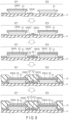
- FIG. 1 shows an example of a configuration of a display device according to a first embodiment.
- FIG. 2 shows an example of a layout of sub-pixels included in a pixel.
- FIG. 3 shows another example of a layout of sub-pixels included in a pixel.
- FIG. 4 shows an example of a cross section of a display area included in a display device according to a comparative example of the present embodiment.
- FIG. 5 is a drawing for explaining a process by which an organic layer and a second electrode are formed in the display device according to the comparative example of the present embodiment.
- FIG. 6 shows an example of a cross section of a display area included in the display device according to the present embodiment.
- FIG. 7 is a schematic plan view of a sub-pixel in the present embodiment.
- FIG. 8 is a diagram for explaining a process by which an organic layer, a second electrode, and a third electrode are formed in the display device according to the present embodiment.
- FIG. 9 is an enlarged view of edge portions of the organic layer and the second electrode in the display device according to the present embodiment.
- FIG. 10 is an enlarged view of edge portions of the organic layer and the second electrode in the display device according to the comparative example of the present embodiment.
- FIG. 11 shows an example of a cross section of a display area included in a display device according to a second embodiment.
- FIG. 12 is a drawing for explaining a process by which an organic layer and a third electrode are formed in the display device according to the present embodiment.
- FIG. 13 is an enlarged view of an edge portion of the organic layer in the display device according to the present embodiment.
- a display device includes a base material, a first insulating layer disposed on the substrate, a first electrode disposed on the first insulating layer, an organic layer disposed on the first electrode, a second electrode disposed on the organic layer, a second insulating layer disposed on the first insulating layer and including an opening portion overlapping with the second electrode, and a third electrode covering the second electrode and the second insulating layer.
- the first electrode, the organic layer, and the second electrode are separated for each pixel.
- FIG. 1 A direction along the X axis is referred to as an X direction or a first direction
- a direction along the Y axis is referred to as a Y direction or a second direction
- direction along the Z axis is referred to as a Z direction or a third direction.
- viewing towards an X-Y plane defined by the X axis and the Y axis is referred to as planar view.
- the third direction Z is referred to as “upward” and a direction opposite to the third direction is referred to as “downward”.
- a display device DSP is an organic electroluminescent display device including an organic light-emitting diode (OLED) as a display element, and is mounted on a television, a personal computer, a mobile terminal, and a cell phone, etc.
- OLED organic light-emitting diode
- FIG. 1 shows an example of a configuration of a display device DSP in the present embodiment.
- the display device DSP includes a display area DA for displaying an image on an insulating base material 10 .
- the base material 10 may be glass or a flexible resin film.
- the display area DA includes a plurality of pixels PX arranged in a matrix in a first direction X and a second direction Y.
- a pixel PX includes, for example, a plurality of sub-pixels SP.
- the pixel PX includes a sub-pixel SP 1 for displaying red, a sub-pixel SP 2 for displaying green, and a sub-pixel SP 3 for displaying blue.
- the pixel PX may include four or more sub-pixels SP including sub-pixels for displaying other colors such as white in addition to the above three sub-pixels.
- the sub-pixel SP includes a pixel circuit 1 and a display element 20 .
- the pixel circuit 1 includes a pixel switch 2 , a drive transistor 3 , and a capacitor 4 .
- the pixel switch 2 and the drive transistor 3 are switch elements configured by, for example, a thin film transistor (TFT).
- TFT thin film transistor
- a gate electrode is connected to a scanning line GL
- a source electrode is connected to a signal line SL
- a drain electrode is connected to one of the electrodes configuring the capacitor 4 and a gate electrode of the drive transistor 3 .
- a source electrode is connected to the other electrode configuring the capacitor 4 and a power line PL
- a drain electrode is connected to an anode electrode of the display element 20 .
- a cathode electrode of the display element 20 is connected to a power supply line FL. Note that the configuration of the pixel circuit 1 is not limited to the illustrated example.
- the display element 20 is an organic light-emitting diode (OLED), which is a light-emitting element.
- OLED organic light-emitting diode
- the display element 20 included in the sub-pixel SP 1 is configured to emit light corresponding to a red wavelength.
- the display element 20 included in the sub-pixel SP 2 is configured to emit light corresponding to a green wavelength.
- the display element 20 included in the sub-pixel SP 3 is configured to emit light corresponding to a blue wavelength.
- the configuration of the display element 20 will be described later.
- FIG. 2 shows an example of a layout of a plurality of sub-pixels SP (SP 1 , SP 2 , and SP 3 ) included in a pixel PX.
- SP sub-pixels
- the sub-pixels SP 1 , SP 2 , and SP 3 which configure one pixel PX, are formed approximately in a rectangular shape extending respectively in the second direction Y, and are arranged side by side in the first direction X. Focusing on two pixels PX arranged side by side in the first direction X, the colors displayed in the adjacent sub-pixels SP are different from each other. Furthermore, focusing on two pixels PX arranged side by side in the second direction Y, the colors displayed in the adjacent sub-pixels SP are the same. Note that the area of each of the sub-pixels SP 1 , SP 2 , and SP 3 may be the same or different from each other.
- FIG. 3 shows another example of the layout of a plurality of sub-pixels SP (SP 1 , SP 2 , and SP 3 ) included in a pixel PX.
- the sub-pixels SP 1 and SP 2 are arranged side by side in the second direction Y
- the sub-pixels SP 1 and SP 3 are arranged side by side in the first direction X
- the sub-pixels SP 2 and SP 3 are arranged side by side in the first direction X.
- the sub-pixel SP 1 is formed approximately in a rectangular shape extending in the first direction X
- the sub-pixels SP 2 and SP 3 are formed approximately in a rectangular shape extending in the second direction Y.
- the area of sub-pixel SP 2 is larger than the area of sub-pixel SP 1
- the area of sub-pixel SP 3 is larger than the area of sub-pixel SP 2 .
- the area of sub-pixel SP 1 may be the same as the area of sub-pixel SP 2 .
- the colors displayed in the sub-pixels SP adjacent in the first direction X are different from each other.
- the colors emitted by the sub-pixels SP adjacent in the second direction Y will be the same as each other.
- the colors displayed in the sub-pixels SP adjacent in the second direction Y are the same.
- the outline of the sub-pixels SP (SP 1 , SP 2 , and SP 3 ) shown in FIG. 2 and FIG. 3 corresponds to the outline of areas in which colors are displayed in the sub-pixels SP (i.e., a light-emitting area); however, the outline is in a simplified form, and does not necessarily reflect the actual shape.
- a display device DSP′ according to a comparative example of the present embodiment with be explained with reference to FIG. 4 . It is assumed that the display device DSP′ has the same configuration as the display device DSP shown in FIG. 1 , and configurations in common with the display device DSP are described with the same reference symbols as those in FIG. 1 .
- FIG. 4 shows an example of a cross section of the display area DA included in the display device DSP′.
- the sub-pixel SP 1 and the sub-pixel SP 2 adjacent to the sub-pixel SP 1 which are provided in the pixel PX disposed in the display area DA, are mainly explained.
- An insulating layer 11 is disposed on a base material 10 .
- the pixel circuit 1 shown in FIG. 1 is disposed on the base material 10 and covered by the insulating layer 11 ; however, this is omitted in FIG. 4 .
- the insulating layer 11 corresponds to the base layer of the display element 20 and is, for example, an organic insulating layer.
- the insulating layer 12 is disposed on top of the insulating layer 11 .
- the insulating layer 12 is, for example, an organic insulating layer.
- An insulating layer 12 is formed to partition the display elements 20 (i.e., sub-pixels SP) included in each of the plurality of sub-pixels SP, and may be referred to as a rib or the like, for example.
- the display element 20 includes a first electrode E 1 , an organic layer OR, and a second electrode E 2 .
- the first electrode E 1 is an electrode arranged for each display element 20 (i.e., sub-pixel SP) included in each of the plurality of sub-pixels SP, and may be referred to as a pixel electrode, bottom electrode, or anode electrode, etc.
- the second electrode E 2 is an electrode commonly arranged for a plurality of display elements (i.e., a plurality of sub-pixels SP or pixels PX), and may be referred to as a common electrode, a counter electrode, an upper electrode, or a cathode electrode, etc.
- the first electrode E 1 is disposed on the insulating layer 11 , and its periphery is covered by the insulating layer 12 .
- the first electrode E 1 is electrically connected to the drive transistor 3 .
- the first electrode E 1 is a transparent electrode formed by a transparent conductive material such as indium tin oxide (ITO) or indium zinc oxide (IZO).
- ITO indium tin oxide
- IZO indium zinc oxide
- the first electrode E 1 may also be a metal electrode formed by a metallic material such as silver or aluminum.
- the first electrode E 1 may be a stacked layer body of a transparent electrode and a metal electrode.
- the first electrode E 1 may be configured as a stacked layer body in which a transparent electrode, a metal electrode, and a transparent electrode are stacked in that order, or may be configured as a stacked layer body including three or more layers.
- the insulating layer 12 has an opening portion OP that overlaps with the first electrode E 1 in each sub-pixel SP.
- the organic layer OR is disposed on the insulating layer 12 and is in contact with the first electrode E 1 through the opening portion OP.
- the second electrode E 2 is disposed on the organic layer OR so as to cover the organic layer OR.
- the second electrode E 2 is a transparent electrode formed by a transparent conductive material such as ITO or IZO, for example.
- the second electrode E 2 is electrically connected to the power supply line FL disposed in the display area DA or outside the display area DA.
- the second electrode E 2 may be covered by a transparent protective film (including at least one of an inorganic insulating film and an organic insulating film).
- the sub-pixel SP 1 includes a display element 20 (hereinafter referred to as the display element 20 of the sub-pixel SP 1 ) including the first electrode E 1 , the organic layer OR, and (a part of) the second electrode E 2 disposed at a position overlapping with the sub-pixel SP 1 .
- the sub-pixel SP 2 includes a display element 20 (hereinafter referred to as the display element 20 of the sub-pixel SP 2 ) including the first electrode E 1 , the organic layer OR, and (a part of) the second electrode E 2 disposed at a position overlapping with the sub-pixel SP 2 .
- the organic layer OR provided in the display element 20 of the sub-pixel SP 1 has a light-emitting layer that emits red.
- the organic layer OR provided in the display element 20 of the sub-pixel SP 2 has a light-emitting layer that emits green.
- the light-emitting layer of the organic layer OR emits light when a potential difference is formed between the first and second electrodes E 1 and E 2 (i.e., a drive current is supplied).
- the display element 20 of the sub-pixel SP 3 is also configured in the same manner as the display elements 20 of the sub-pixels SP 1 and SP 2 . That is, in the case where the sub-pixel SP 3 displays blue, the organic layer OR provided in the display element 20 of the sub-pixel SP 3 has a light-emitting layer that emits blue.
- the organic layer OR is formed on the first electrode E 1 . Furthermore, in the display element 20 of the sub-pixel SP 1 (i.e., a position overlapping with the sub-pixel SP 1 ), it is necessary to form an organic layer OR including a light-emitting layer that emits red (hereinafter referred to as an organic layer OR(R)). On the other hand, in the display element 20 of the sub-pixel SP 2 (i.e., a position overlapping with the sub-pixel SP 2 ), it is necessary to form an organic layer OR including a light-emitting layer that emits green (hereinafter referred to as an organic layer OR(G)).
- the organic layer OR(R) disposed at the position overlapping with the sub-pixel SP 1 and the organic layer OR(G) disposed at the position overlapping with the sub-pixel SP 2 can be formed by patterning using, for example, a fine mask.
- the edge portion of the organic layer OR(R) may overlap with the edge portion of the organic layer OR(G).
- a current may flow from the edge portion of the organic layer OR(G) to the organic layer OR(R), causing the light-emitting layer of the organic layer OR(R) to emit light (hereinafter referred to as parasitic emission).
- the parasitic emission based on such lateral leakage may cause color mixing, etc., and may be a cause of deteriorating display quality.
- the present embodiment has a configuration for suppressing the occurrence of the above-mentioned lateral leakage.
- FIG. 6 shows an example of a cross section of the display area DA provided in the display device DSP.
- the sub-pixel SP 1 and the sub-pixel SP 2 adjacent to the sub-pixel SP 1 which are provided in the pixel PX located in the display area DA, are mainly explained.
- parts that are the same as those in FIG. 4 are given the same reference symbols as those in FIG. 4 above, and detailed descriptions thereof are omitted. Parts that are different from those in FIG. 4 are mainly described.
- the first electrode E 1 is placed on the insulating layer 11 in the same manner as in the comparative example of the present embodiment described above.
- the first electrode E 1 in the present embodiment differs from the first electrode E 1 in the comparative example in that the edge portion of the first electrode E 1 is not covered by the insulating layer 12 when the organic layer OR is formed.
- the first electrode E 1 in the present embodiment is assumed to be formed at least thicker than the organic layer OR, and the organic layer OR is, for example, about 10 nm, the first electrode E 1 in the present embodiment is formed at about 100 nm.
- the organic layer OR is disposed on the first electrode E 1
- the second electrode E 2 is disposed on the organic layer OR.
- the insulating layer 12 is disposed on the insulating layer 11 and has an opening portion OP that overlaps with the second electrode E 2 .
- the third electrode E 3 is disposed in a manner covering the second electrode E 2 and the insulating layer 12 .
- FIG. 7 is a schematic plan view of the sub-pixels SP 1 and SP 2 shown in FIG. 6 .
- the insulating layer 12 has an opening portion OP for each of the sub-pixels SP 1 and SP 2 , and the first electrode E 1 , the organic layer OR, and the second electrode E 2 are disposed at positions overlapping with the opening portion OP.
- the portion at which the first electrode E 1 , the organic layer OR, and the second electrode E 2 overlap functions as a light-emitting part of each sub-pixel SP (SP 1 and SP 2 ), and light of the color corresponding to the sub-pixel SP can be emitted from the light-emitting part.
- the insulating layer 12 by forming the insulating layer 12 with a transparent organic material, light can be emitted (extracted) from an area one size larger than the opening portion OP, and a high aperture ratio can be achieved.
- the third electrode E 3 is omitted.
- the organic layer OR (R) is formed (deposited) on the first electrode E 1 , which is disposed at a position that overlaps with the sub-pixel SP 1 .
- the first electrode E 1 is formed to be sufficiently thicker than the organic layer OR(R). Therefore, in the case of attempting to form the organic layer OR(R) at the position that overlaps with the sub-pixel SP 1 , the organic layer OR(R) is cut off at the edge portion of the first electrode E 1 that is disposed at the position that overlaps with the sub-pixel SP 1 , and the organic layer OR(R) is formed in an island shape on the first electrode E 1 . In this case, an organic layer OR(R)′ that is cut off at the edge portion of the first electrode E 1 is disposed on the insulating layer 11 .
- the organic layer OR(G) is formed (deposited) on the first electrode E 1 that is disposed at a position that overlaps with the sub-pixel SP 2 .
- the first electrode E 1 is formed sufficiently thicker than the organic layer OR(G). Therefore, in the case of attempting to form the organic layer OR(G) at the position that overlaps with the sub-pixel SP 1 , the organic layer OR(G) is cut off at the edge portion of the first electrode E 1 that is disposed at the position that overlaps with the sub-pixel SP 2 , and the organic layer OR(G) is formed in an island shape on the first electrode E 1 . In this case, an organic layer OR(G)′ that is cut off at the edge portion of the first electrode E 1 is disposed on the insulating layer 11 .
- the second electrode E 2 is formed (deposited) on the organic layers OR(R) and OR(G). Since the present embodiment has a configuration in which the above mentioned first electrode E 1 causes the organic layers OR(R)′ and OR(G)′ to be cut off, for example, by forming the second electrode E 2 over the entire display area DA, the second electrode E 2 , separated for each sub-pixel SP, can be disposed on the first electrode E 1 and the organic layer OR.
- a second electrode E 2 ′, which is cut off at the edge portion of the first electrode E 1 is disposed on the organic layers OR(R)′ and OR(G)′ disposed on the insulating layer 11 .
- the organic layer OR and the second electrode E 2 can be formed separately for each sub-pixel SP.
- the first electrode E 1 in order to facilitate cutting off the organic layer OR and the second electrode E 2 , it is preferable to form the first electrode E 1 in a manner such that the width of the upper part is greater than that of the lower part.
- the first electrode E 1 is formed in a manner such that the width gradually decreases from the upper part to the lower part.
- the first electrode E 1 may be formed as a stacked layer body of a transparent electrode and a metal electrode (e.g., Ag, etc.).
- the first electrode E 1 can be formed as shown in FIG. 6 and FIG. 8 by forming the first electrode E 1 in a shape where the width of the upper part matches the width of the lower part, then removing the part configured by the metal electrode by side etching, etc.
- the first electrode E 1 may be formed by other processes as well.
- the first electrode E 1 may have a shape such as, for example, an inverted taper shape. Furthermore, the side surface of the first electrode E 1 may be a plane inclined with respect to a third direction Z, or may be a curved surface.
- the insulating layer 12 that is disposed on the insulating layer 11 to cover the edge portions of the organic layers OR(R) and OR(G) and the second electrode E 2 , and has an opening portion OP that overlaps with the second electrode E 2 is formed.
- the second electrode E 2 is an electrode for applying a common voltage to a plurality of sub-pixels SP (a plurality of pixels PX), and according to the process shown in FIG. 8 above, the second electrode E 2 is formed in an island shape for each sub-pixel SP.
- the second electrodes E 2 formed in such an island shape it is necessary to, for example, connect the second electrodes E 2 formed at a position (area) that overlaps with each of the adjacent sub-pixels SP (e.g., sub-pixels SP 1 and SP 2 ).
- the third electrode E 3 for connecting the two electrodes is formed (deposited) in a manner covering the second electrode E 2 and the insulating layer 12 .
- Such a third electrode E 3 is to be formed over a plurality of pixels PX (sub-pixels SP) arranged in the display area DA. According to this third electrode E 3 , a common voltage can be applied to each of the sub-pixels SP through the second electrode E 2 , which is formed in an island shape at a position that overlaps with each of the plurality of sub-pixels SP.
- the sub-pixels SP 1 and SP 2 are mainly described; however, the sub-pixel SP 3 is also to be configured in the same manner as the sub-pixels SP 1 and SP 2 .
- the display device DSP includes a base material 10 , an insulating layer 11 (first insulating layer) disposed on the base material 10 , a first electrode E 1 disposed on the insulating layer 11 , an organic layer OR disposed on the first electrode E 1 , a second electrode E 2 disposed on the organic layer, an insulating layer 12 disposed on the insulating layer 11 and having an opening portion OP that overlaps with the second electrode E 2 , and a third electrode E 3 covering the second electrode E 2 and the insulating layer 12 .
- the first electrode E 1 , the organic layer OR, and the second electrode E 2 are separated for each sub-pixel SP.
- lateral leakage may occur when the edge portion of the organic layer OR (R) of the sub-pixel SP 1 overlaps with the edge portion of the organic layer OR (G) of the sub-pixel SP 2 adjacent to the sub-pixel SP 1 .
- the organic layer OR (R) of the sub-pixel SP 1 and the organic layer OR (G) of the sub-pixel SP 2 are separated for each sub-pixel SP, thus preventing the occurrence of parasitic emission based on the lateral leakage and suppressing the deterioration of display quality.
- the second electrodes E 2 formed at a position that overlaps with the sub-pixel SP are connected through the third electrode E 3 . That is, in the present embodiment, even if the second electrode E 2 is configured to be separated for each sub-pixel SP, the display device DSP (the second electrode E 2 provided in the display device DSP) can be driven normally by the third electrode E 3 .
- the organic layer OR (and the second electrode E 2 ) can be cut off, and the organic layer OR can be separated appropriately for each sub-pixel SP.
- the first electrode E 1 described above is formed in such a way that, for example, the width of the upper part is larger than that of the lower part.
- the first electrode E 1 separates the organic layer OR (and the second electrode E 2 ) for each sub-pixel SP.
- at least the organic layer OR needs to be separated for each sub-pixel SP to prevent the occurrence of lateral leakage, and the separation of the organic layer OR may be realized by means other than the first electrode E 1 .
- FIG. 9 shows an enlarged view of the edge portions (periphery) of the organic layer OR and the second electrode E 2 in the display device DSP according to the present embodiment.
- the organic layer OR includes, for example, a functional layer F 1 , a light-emitting layer EL, and a functional layer F 2 , which are stacked in order from the first electrode E 1 to the second electrode E 2 .
- the first electrode E 1 corresponds to the anode and the second electrode E 2 corresponds to the cathode.
- the functional layer F 1 between the light-emitting layer EL and the first electrode E 1 includes at least one of a hole injection layer and a hole transport layer
- the functional layer F 2 between the light-emitting layer EL and the second electrode E 2 includes at least one of an electron transport layer and an electron injection layer.
- Each of the functional layers F 1 and F 2 is not limited to a single-layer body, but may also be a stacked layer body in which a plurality of functional layers are stacked.
- first electrode E 1 corresponds to the anode and the second electrode E 2 corresponds to the cathode
- first electrode E 1 corresponds to the cathode
- second electrode E 2 corresponds to the anode
- the organic layer OR is described as including the functional layer F 1 , the light-emitting layer EL, and the functional layer F 2 , the organic layer OR may further include other functional layers, or may have a configuration in which at least one of the functional layers F 1 and F 2 is omitted.
- FIG. 9 an example is shown in which the end surfaces of each of the organic layers OR (the functional layer F 1 , the light-emitting layer EL, and the functional layer F 2 ) and the second electrode E 2 are substantially aligned.
- FIG. 10 shows, as a comparative example of the present embodiment, an example in which the end surfaces (edge portions) of the functional layer F 1 , the light-emitting layer EL, and the functional layer F 2 included in the organic layer OR are covered by the second electrode E 2 disposed on the organic layer OR (in contact with the second electrode E 2 ).
- the organic layer OR and the second electrode E 2 are configured in the manner shown in FIG. 10 , a current that does not contribute to the emission of the light-emitting layer EL (edge leakage) is generated from the edge portion of the organic layer OR (the functional layer F 1 , the light-emitting layer EL, and functional layer F 2 ). This edge leakage may cause the performance of the display device DSP to deteriorate.
- the second electrode E 2 is formed in a manner such that the second electrode E 2 does not cover the end surfaces of the functional layer F 1 , the light-emitting layer EL, and the functional layer F 2 provided in the organic layer OR (the end surfaces of the functional layer F 1 , the light-emitting layer EL, and the functional layer F 2 do not come in contact with the second electrode E 2 ).
- the organic layer OR and the second electrode E 2 in the present embodiment are formed so that the edge portion (end surface) of the second electrode E 2 matches the end surface of the organic layer OR in a plan view or is on the opening portion OP side (i.e., the center side of the sub-pixel SP) than the end surface of the organic layer OR is.
- the second electrode E 2 can be formed, for example, by a directional vacuum deposition method.
- the second electrode that does not cover the end surfaces of the functional layer F 1 , the light-emitting layer EL, and the functional layer F 2 provided in the organic layer OR described above can be formed by considering the directivity in the vacuum deposition method.
- FIG. 9 an example in which the end surfaces of the functional layer F 1 , the light-emitting layer EL, and the functional layer F 2 provided in the organic layer OR are substantially aligned.
- the second electrode E 2 is formed so that it does not cover the end surfaces of the functional layer F 1 , the light-emitting layer EL, and the functional layer F 2 as described above, the end surfaces of each of the functional layer F 1 , the light-emitting layer EL, and the functional layer F 2 do not have to be aligned.
- the pixel PX includes sub-pixels SP 1 , SP 2 and SP 3 , and each of the sub-pixels SP 1 , SP 2 and SP 3 includes a display element 20 that emits light corresponding to red, green and blue wavelengths.
- the display element 20 of each of the sub-pixels SP 1 , SP 2 and SP 3 may also emit, for example, white light.
- red, green, and blue light can be emitted from each pixel PX, thus enabling multi-color display.
- Each of the sub-pixels SP 1 , SP 2 , and SP 3 described above may be provided with a display element 20 that emits ultraviolet light (i.e., the emitting color is ultraviolet light).
- a display element 20 that emits ultraviolet light (i.e., the emitting color is ultraviolet light).
- multi-color display can be realized by disposing a light conversion layer at a position facing the display element 20 .
- the pixel PX has been explained as including a plurality of sub-pixels SP, the pixel PX may be configured not to include the sub-pixels SP (i.e., a single color is displayed by the pixel PX).
- an organic layer OR i.e., for example, an organic layer OR including a light-emitting layer emitting white color
- a configuration including a first electrode E 1 capable of cutting off the organic layer OR and by depositing the organic layer OR (organic material for forming the organic layer OR) on the entire DA, it is possible to form an organic layer OR separated for each pixel PX (sub-pixel SP).
- the present embodiment can be applied to WOLEDs, etc., in which the organic layer OR is not separated, and in such a configuration, there is no need to use a fine mask, etc., when forming the organic layer OR (i.e., separating the organic layer OR for each pixel PX or sub-pixel SP).
- FIG. 11 shows an example of a cross-section of a display area provided in a display device of the present embodiment.
- a sub-pixel SP 1 and a sub-pixel SP 2 adjacent to the sub-pixel SP 1 which are provided in a pixel PX disposed in a display area DA, are mainly described.
- FIG. 11 parts that are the same as those in FIG. 6 are given the same reference symbols as those in FIG. 6 above, and detailed descriptions thereof are omitted. Parts that differ from FIG. 6 are described.
- the second electrode E 2 is disposed on the organic layer OR, and the third electrode E 3 is formed to cover the second electrode E 2 and the insulating layer 12 .
- the present embodiment differs from the first embodiment in that the second electrode E 2 is omitted, and the third electrode E 3 is formed to cover the organic layer OR and the insulating layer 12 .
- a display device DSP shown in FIG. 11 is similar to the display device DSP shown in FIG. 6 above except that the second electrode E 2 is omitted as described above, here, a detailed description thereof is omitted.
- an organic layer OR (R) is formed (deposited) on the first electrode E 1 , which is disposed at a position overlapping with the sub-pixel SP 1 .
- the organic layer OR(R) is disposed on the first electrode E 1
- an organic layer OR(R)′ which is cut off at the edge portion of the first electrode E 1 , is disposed on the insulating layer 11 .
- an organic layer OR(G) is formed (deposited) on the first electrode E 1 disposed at a position overlapping with the sub-pixel SP 2 .
- the organic layer OR(G) is disposed on the first electrode E 1
- an organic layer OR(G)′ which is cut off at the edge portion of the first electrode E 1 , is disposed on the insulating layer 11 .
- the insulating layer 12 that is disposed on the insulating layer 11 to cover the edge portions of the organic layers OR(R) and OR(G), and has an opening portion OP that overlaps with the organic layer OR is formed.
- the third electrode E 3 is formed (deposited) over a plurality of pixels PX (sub-pixels SP) disposed in the display area DA. According to such a third electrode, a common voltage can be applied to each of the plurality of pixels PX.
- the sub-pixels SP 1 and SP 2 are mainly described; however, a sub-pixel SP 3 is also to be configured in the same manner as the sub-pixels SP 1 and SP 2 .
- the display device DSP includes a base material 10 , an insulating layer 11 (first insulating layer) disposed on the base material 10 , a first electrode E 1 disposed on the insulating layer 11 , an organic layer OR disposed on the first electrode E 1 , an insulating layer 12 (second insulating layer) disposed on the insulating layer 11 and having an opening portion OP that overlaps with the organic layer OR, and a third electrode E 3 (second electrode) covering the organic layer OR and the insulating layer 12 .
- the first electrode E 1 and the organic layer OR are separated for each sub-pixel SP.
- the above-described configuration prevents the occurrence of parasitic emission based on lateral leakage and suppresses the deterioration of display quality, as in the first embodiment.
- FIG. 13 shows an enlarged view of the edge portion (periphery) of the organic layer OR in the display device DSP of the present embodiment.
- the end surfaces (edge portions) of a functional layer F 1 , a light-emitting layer EL, and a functional layer F 2 included in the organic layer OR are covered by the insulating layer 12 , so that no edge leakage occurs from the organic layer OR.
- edge leakage may occur from the organic layer OR when the organic layer OR and the second electrode E 2 are formed in the manner shown in, for example, FIG. 10 .
- the occurrence of edge leakage from the organic layer OR can be prevented more reliably, which is an advantage compared to the first embodiment.
- a configuration in which a second electrode E 2 is provided to protect the display element 20 (e.g., organic layer OR) in the process of forming the third electrode E 3 is adopted.
- the configuration of the present embodiment can be adopted, and the manufacturing process of the display device DSP can be simplified compared to the first embodiment described above.
- the display device DSP of the present embodiment may be configured to include a color filter or a light conversion layer, as in the first embodiment described above, or the pixel PX may be configured not to include a sub-pixel SP.
Landscapes
- Physics & Mathematics (AREA)
- Optics & Photonics (AREA)
- Engineering & Computer Science (AREA)
- Manufacturing & Machinery (AREA)
- Microelectronics & Electronic Packaging (AREA)
- Electroluminescent Light Sources (AREA)
- Devices For Indicating Variable Information By Combining Individual Elements (AREA)
Abstract
Description
Claims (3)
Applications Claiming Priority (2)
| Application Number | Priority Date | Filing Date | Title |
|---|---|---|---|
| JP2021012185A JP7585062B2 (en) | 2021-01-28 | 2021-01-28 | Display device |
| JP2021-012185 | 2021-01-28 |
Publications (2)
| Publication Number | Publication Date |
|---|---|
| US20220238835A1 US20220238835A1 (en) | 2022-07-28 |
| US12200954B2 true US12200954B2 (en) | 2025-01-14 |
Family
ID=82495082
Family Applications (1)
| Application Number | Title | Priority Date | Filing Date |
|---|---|---|---|
| US17/585,759 Active 2043-02-16 US12200954B2 (en) | 2021-01-28 | 2022-01-27 | Display device |
Country Status (2)
| Country | Link |
|---|---|
| US (1) | US12200954B2 (en) |
| JP (1) | JP7585062B2 (en) |
Families Citing this family (2)
| Publication number | Priority date | Publication date | Assignee | Title |
|---|---|---|---|---|
| WO2025158482A1 (en) * | 2024-01-22 | 2025-07-31 | シャープディスプレイテクノロジー株式会社 | Display device and method for manufacturing display device |
| FR3161088A1 (en) * | 2024-04-04 | 2025-10-10 | Commissariat A L' Energie Atomique Et Aux Energies Alternatives | METHOD FOR MANUFACTURING ELECTROLUMINESCENT DISPLAY DEVICE, ELECTROLUMINESCENT DISPLAY DEVICE |
Citations (12)
| Publication number | Priority date | Publication date | Assignee | Title |
|---|---|---|---|---|
| JP2000195677A (en) | 1998-12-25 | 2000-07-14 | Tdk Corp | Organic EL display device and manufacturing method thereof |
| JP2004207217A (en) | 2002-12-11 | 2004-07-22 | Sony Corp | Display device and method of manufacturing display device |
| JP2008135325A (en) | 2006-11-29 | 2008-06-12 | Hitachi Displays Ltd | Organic EL display device and manufacturing method thereof |
| US20090009069A1 (en) | 2007-07-03 | 2009-01-08 | Canon Kabushiki Kaisha | Organic el display apparatus and method of manufacturing the same |
| JP2009032673A (en) | 2007-07-03 | 2009-02-12 | Canon Inc | Organic EL display device and manufacturing method thereof |
| JP2010118191A (en) | 2008-11-11 | 2010-05-27 | Sharp Corp | Organic electroluminescent display device and its manufacturing method |
| JP2013089505A (en) | 2011-10-19 | 2013-05-13 | Sony Corp | Display panel, display device and electronic apparatus |
| US20150048328A1 (en) * | 2013-05-29 | 2015-02-19 | Sony Corporation | Display unit, method of manufacturing display unit, and electronic apparatus |
| US20170271421A1 (en) | 2016-03-18 | 2017-09-21 | Semiconductor Energy Laboratory Co., Ltd. | Display device |
| CN109509765B (en) * | 2017-09-14 | 2021-12-31 | 维信诺科技股份有限公司 | Organic light-emitting display screen and manufacturing method thereof |
| US20220102669A1 (en) * | 2020-01-06 | 2022-03-31 | Boe Technology Group Co., Ltd. | Organic electroluminescent structure and fabrication method thereof, and display device |
| WO2022123383A1 (en) | 2020-12-07 | 2022-06-16 | 株式会社半導体エネルギー研究所 | Method for producing display device |
-
2021
- 2021-01-28 JP JP2021012185A patent/JP7585062B2/en active Active
-
2022
- 2022-01-27 US US17/585,759 patent/US12200954B2/en active Active
Patent Citations (16)
| Publication number | Priority date | Publication date | Assignee | Title |
|---|---|---|---|---|
| JP2000195677A (en) | 1998-12-25 | 2000-07-14 | Tdk Corp | Organic EL display device and manufacturing method thereof |
| JP2004207217A (en) | 2002-12-11 | 2004-07-22 | Sony Corp | Display device and method of manufacturing display device |
| US20040160170A1 (en) | 2002-12-11 | 2004-08-19 | Chiyoko Sato | Display apparatus and method of manufacturing the same |
| JP2008135325A (en) | 2006-11-29 | 2008-06-12 | Hitachi Displays Ltd | Organic EL display device and manufacturing method thereof |
| US20090009069A1 (en) | 2007-07-03 | 2009-01-08 | Canon Kabushiki Kaisha | Organic el display apparatus and method of manufacturing the same |
| JP2009032673A (en) | 2007-07-03 | 2009-02-12 | Canon Inc | Organic EL display device and manufacturing method thereof |
| JP2010118191A (en) | 2008-11-11 | 2010-05-27 | Sharp Corp | Organic electroluminescent display device and its manufacturing method |
| JP2013089505A (en) | 2011-10-19 | 2013-05-13 | Sony Corp | Display panel, display device and electronic apparatus |
| US20140231789A1 (en) | 2011-10-19 | 2014-08-21 | Sony Corporation | Display panel, display unit, and electronic apparatus |
| US20150048328A1 (en) * | 2013-05-29 | 2015-02-19 | Sony Corporation | Display unit, method of manufacturing display unit, and electronic apparatus |
| US20170271421A1 (en) | 2016-03-18 | 2017-09-21 | Semiconductor Energy Laboratory Co., Ltd. | Display device |
| JP2017174811A (en) | 2016-03-18 | 2017-09-28 | 株式会社半導体エネルギー研究所 | Display device |
| CN109509765B (en) * | 2017-09-14 | 2021-12-31 | 维信诺科技股份有限公司 | Organic light-emitting display screen and manufacturing method thereof |
| US20220102669A1 (en) * | 2020-01-06 | 2022-03-31 | Boe Technology Group Co., Ltd. | Organic electroluminescent structure and fabrication method thereof, and display device |
| WO2022123383A1 (en) | 2020-12-07 | 2022-06-16 | 株式会社半導体エネルギー研究所 | Method for producing display device |
| US20240023371A1 (en) * | 2020-12-07 | 2024-01-18 | Semiconductor Energy Laboratory Co., Ltd. | Method For Fabricating Display Apparatus |
Non-Patent Citations (1)
| Title |
|---|
| Office Action issued on Aug. 20, 2024, in corresponding Japanese Application No. 2021-012185, 6 pages. |
Also Published As
| Publication number | Publication date |
|---|---|
| JP7585062B2 (en) | 2024-11-18 |
| JP2022115548A (en) | 2022-08-09 |
| US20220238835A1 (en) | 2022-07-28 |
Similar Documents
| Publication | Publication Date | Title |
|---|---|---|
| US12108631B2 (en) | Display device | |
| US12262580B2 (en) | Display device including an organic light-emitting diode (OLED) | |
| US12185595B2 (en) | Display device | |
| US12317694B2 (en) | Display device | |
| US11997907B2 (en) | Display device | |
| US12268069B2 (en) | Display device | |
| US20250160188A1 (en) | Display device | |
| US12464898B2 (en) | Display device including an electrode covering an insulator, barrier walls, and a second electrode | |
| US12484386B2 (en) | Display device | |
| US20250268089A1 (en) | Display device | |
| US12200954B2 (en) | Display device | |
| US20230422550A1 (en) | Display device | |
| US12369465B2 (en) | Display device | |
| US12342684B2 (en) | Display device | |
| US20230403916A1 (en) | Display device | |
| US20230389360A1 (en) | Display device | |
| US20250294974A1 (en) | Display device | |
| US20240334748A1 (en) | Display device | |
| US20240341123A1 (en) | Display device | |
| US20250204167A1 (en) | Display device |
Legal Events
| Date | Code | Title | Description |
|---|---|---|---|
| AS | Assignment |
Owner name: JAPAN DISPLAY INC., JAPAN Free format text: ASSIGNMENT OF ASSIGNORS INTEREST;ASSIGNOR:TAKAHASHI, HIDEYUKI;REEL/FRAME:058789/0913 Effective date: 20220121 |
|
| FEPP | Fee payment procedure |
Free format text: ENTITY STATUS SET TO UNDISCOUNTED (ORIGINAL EVENT CODE: BIG.); ENTITY STATUS OF PATENT OWNER: LARGE ENTITY |
|
| STPP | Information on status: patent application and granting procedure in general |
Free format text: DOCKETED NEW CASE - READY FOR EXAMINATION |
|
| STPP | Information on status: patent application and granting procedure in general |
Free format text: NON FINAL ACTION MAILED |
|
| STPP | Information on status: patent application and granting procedure in general |
Free format text: RESPONSE TO NON-FINAL OFFICE ACTION ENTERED AND FORWARDED TO EXAMINER |
|
| STPP | Information on status: patent application and granting procedure in general |
Free format text: FINAL REJECTION MAILED |
|
| STPP | Information on status: patent application and granting procedure in general |
Free format text: RESPONSE AFTER FINAL ACTION FORWARDED TO EXAMINER |
|
| STPP | Information on status: patent application and granting procedure in general |
Free format text: NOTICE OF ALLOWANCE MAILED -- APPLICATION RECEIVED IN OFFICE OF PUBLICATIONS |
|
| STPP | Information on status: patent application and granting procedure in general |
Free format text: WITHDRAW FROM ISSUE AWAITING ACTION |
|
| STPP | Information on status: patent application and granting procedure in general |
Free format text: AWAITING TC RESP., ISSUE FEE NOT PAID |
|
| STPP | Information on status: patent application and granting procedure in general |
Free format text: PUBLICATIONS -- ISSUE FEE PAYMENT VERIFIED |
|
| STCF | Information on status: patent grant |
Free format text: PATENTED CASE |
|
| AS | Assignment |
Owner name: MAGNOLIA WHITE CORPORATION, JAPAN Free format text: ASSIGNMENT OF ASSIGNORS INTEREST;ASSIGNOR:JAPAN DISPLAY INC.;REEL/FRAME:072130/0313 Effective date: 20250625 |