US12199018B2 - Direct bonding in microelectronic assemblies - Google Patents
Direct bonding in microelectronic assemblies Download PDFInfo
- Publication number
- US12199018B2 US12199018B2 US17/025,771 US202017025771A US12199018B2 US 12199018 B2 US12199018 B2 US 12199018B2 US 202017025771 A US202017025771 A US 202017025771A US 12199018 B2 US12199018 B2 US 12199018B2
- Authority
- US
- United States
- Prior art keywords
- microelectronic
- metal contact
- microelectronic component
- component
- power
- Prior art date
- Legal status (The legal status is an assumption and is not a legal conclusion. Google has not performed a legal analysis and makes no representation as to the accuracy of the status listed.)
- Active, expires
Links
Images


Classifications
-
- H01L23/49—
-
- H—ELECTRICITY
- H10—SEMICONDUCTOR DEVICES; ELECTRIC SOLID-STATE DEVICES NOT OTHERWISE PROVIDED FOR
- H10W—GENERIC PACKAGES, INTERCONNECTIONS, CONNECTORS OR OTHER CONSTRUCTIONAL DETAILS OF DEVICES COVERED BY CLASS H10
- H10W72/00—Interconnections or connectors in packages
- H10W72/50—Bond wires
-
- H01L23/53228—
-
- H01L23/5385—
-
- H01L23/5386—
-
- H01L24/80—
-
- H—ELECTRICITY
- H05—ELECTRIC TECHNIQUES NOT OTHERWISE PROVIDED FOR
- H05K—PRINTED CIRCUITS; CASINGS OR CONSTRUCTIONAL DETAILS OF ELECTRIC APPARATUS; MANUFACTURE OF ASSEMBLAGES OF ELECTRICAL COMPONENTS
- H05K1/00—Printed circuits
- H05K1/02—Details
- H05K1/11—Printed elements for providing electric connections to or between printed circuits
-
- H—ELECTRICITY
- H10—SEMICONDUCTOR DEVICES; ELECTRIC SOLID-STATE DEVICES NOT OTHERWISE PROVIDED FOR
- H10W—GENERIC PACKAGES, INTERCONNECTIONS, CONNECTORS OR OTHER CONSTRUCTIONAL DETAILS OF DEVICES COVERED BY CLASS H10
- H10W20/00—Interconnections in chips, wafers or substrates
- H10W20/40—Interconnections external to wafers or substrates, e.g. back-end-of-line [BEOL] metallisations or vias connecting to gate electrodes
- H10W20/41—Interconnections external to wafers or substrates, e.g. back-end-of-line [BEOL] metallisations or vias connecting to gate electrodes characterised by their conductive parts
- H10W20/42—Vias, e.g. via plugs
-
- H—ELECTRICITY
- H10—SEMICONDUCTOR DEVICES; ELECTRIC SOLID-STATE DEVICES NOT OTHERWISE PROVIDED FOR
- H10W—GENERIC PACKAGES, INTERCONNECTIONS, CONNECTORS OR OTHER CONSTRUCTIONAL DETAILS OF DEVICES COVERED BY CLASS H10
- H10W20/00—Interconnections in chips, wafers or substrates
- H10W20/40—Interconnections external to wafers or substrates, e.g. back-end-of-line [BEOL] metallisations or vias connecting to gate electrodes
- H10W20/41—Interconnections external to wafers or substrates, e.g. back-end-of-line [BEOL] metallisations or vias connecting to gate electrodes characterised by their conductive parts
- H10W20/44—Conductive materials thereof
- H10W20/4403—Conductive materials thereof based on metals, e.g. alloys, metal silicides
- H10W20/4421—Conductive materials thereof based on metals, e.g. alloys, metal silicides the principal metal being copper
-
- H—ELECTRICITY
- H10—SEMICONDUCTOR DEVICES; ELECTRIC SOLID-STATE DEVICES NOT OTHERWISE PROVIDED FOR
- H10W—GENERIC PACKAGES, INTERCONNECTIONS, CONNECTORS OR OTHER CONSTRUCTIONAL DETAILS OF DEVICES COVERED BY CLASS H10
- H10W70/00—Package substrates; Interposers; Redistribution layers [RDL]
- H10W70/60—Insulating or insulated package substrates; Interposers; Redistribution layers
- H10W70/611—Insulating or insulated package substrates; Interposers; Redistribution layers for connecting multiple chips together
-
- H—ELECTRICITY
- H10—SEMICONDUCTOR DEVICES; ELECTRIC SOLID-STATE DEVICES NOT OTHERWISE PROVIDED FOR
- H10W—GENERIC PACKAGES, INTERCONNECTIONS, CONNECTORS OR OTHER CONSTRUCTIONAL DETAILS OF DEVICES COVERED BY CLASS H10
- H10W70/00—Package substrates; Interposers; Redistribution layers [RDL]
- H10W70/60—Insulating or insulated package substrates; Interposers; Redistribution layers
- H10W70/62—Insulating or insulated package substrates; Interposers; Redistribution layers characterised by their interconnections
- H10W70/65—Shapes or dispositions of interconnections
-
- H—ELECTRICITY
- H10—SEMICONDUCTOR DEVICES; ELECTRIC SOLID-STATE DEVICES NOT OTHERWISE PROVIDED FOR
- H10W—GENERIC PACKAGES, INTERCONNECTIONS, CONNECTORS OR OTHER CONSTRUCTIONAL DETAILS OF DEVICES COVERED BY CLASS H10
- H10W72/00—Interconnections or connectors in packages
-
- H—ELECTRICITY
- H10—SEMICONDUCTOR DEVICES; ELECTRIC SOLID-STATE DEVICES NOT OTHERWISE PROVIDED FOR
- H10W—GENERIC PACKAGES, INTERCONNECTIONS, CONNECTORS OR OTHER CONSTRUCTIONAL DETAILS OF DEVICES COVERED BY CLASS H10
- H10W72/00—Interconnections or connectors in packages
- H10W72/20—Bump connectors, e.g. solder bumps or copper pillars; Dummy bumps; Thermal bumps
-
- H—ELECTRICITY
- H10—SEMICONDUCTOR DEVICES; ELECTRIC SOLID-STATE DEVICES NOT OTHERWISE PROVIDED FOR
- H10W—GENERIC PACKAGES, INTERCONNECTIONS, CONNECTORS OR OTHER CONSTRUCTIONAL DETAILS OF DEVICES COVERED BY CLASS H10
- H10W90/00—Package configurations
-
- H—ELECTRICITY
- H10—SEMICONDUCTOR DEVICES; ELECTRIC SOLID-STATE DEVICES NOT OTHERWISE PROVIDED FOR
- H10W—GENERIC PACKAGES, INTERCONNECTIONS, CONNECTORS OR OTHER CONSTRUCTIONAL DETAILS OF DEVICES COVERED BY CLASS H10
- H10W90/00—Package configurations
- H10W90/401—Package configurations characterised by multiple insulating or insulated package substrates, interposers or RDLs
-
- H—ELECTRICITY
- H10—SEMICONDUCTOR DEVICES; ELECTRIC SOLID-STATE DEVICES NOT OTHERWISE PROVIDED FOR
- H10W—GENERIC PACKAGES, INTERCONNECTIONS, CONNECTORS OR OTHER CONSTRUCTIONAL DETAILS OF DEVICES COVERED BY CLASS H10
- H10W90/00—Package configurations
- H10W90/701—Package configurations characterised by the relative positions of pads or connectors relative to package parts
- H10W90/721—Package configurations characterised by the relative positions of pads or connectors relative to package parts of bump connectors
- H10W90/723—Package configurations characterised by the relative positions of pads or connectors relative to package parts of bump connectors between laterally-adjacent chips
-
- H—ELECTRICITY
- H10—SEMICONDUCTOR DEVICES; ELECTRIC SOLID-STATE DEVICES NOT OTHERWISE PROVIDED FOR
- H10W—GENERIC PACKAGES, INTERCONNECTIONS, CONNECTORS OR OTHER CONSTRUCTIONAL DETAILS OF DEVICES COVERED BY CLASS H10
- H10W90/00—Package configurations
- H10W90/701—Package configurations characterised by the relative positions of pads or connectors relative to package parts
- H10W90/721—Package configurations characterised by the relative positions of pads or connectors relative to package parts of bump connectors
- H10W90/724—Package configurations characterised by the relative positions of pads or connectors relative to package parts of bump connectors between a chip and a stacked insulating package substrate, interposer or RDL
-
- H01L2224/0812—
-
- H01L2224/80001—
-
- H01L2224/80895—
-
- H—ELECTRICITY
- H10—SEMICONDUCTOR DEVICES; ELECTRIC SOLID-STATE DEVICES NOT OTHERWISE PROVIDED FOR
- H10W—GENERIC PACKAGES, INTERCONNECTIONS, CONNECTORS OR OTHER CONSTRUCTIONAL DETAILS OF DEVICES COVERED BY CLASS H10
- H10W70/00—Package substrates; Interposers; Redistribution layers [RDL]
- H10W70/60—Insulating or insulated package substrates; Interposers; Redistribution layers
- H10W70/67—Insulating or insulated package substrates; Interposers; Redistribution layers characterised by their insulating layers or insulating parts
- H10W70/68—Shapes or dispositions thereof
- H10W70/685—Shapes or dispositions thereof comprising multiple insulating layers
-
- H—ELECTRICITY
- H10—SEMICONDUCTOR DEVICES; ELECTRIC SOLID-STATE DEVICES NOT OTHERWISE PROVIDED FOR
- H10W—GENERIC PACKAGES, INTERCONNECTIONS, CONNECTORS OR OTHER CONSTRUCTIONAL DETAILS OF DEVICES COVERED BY CLASS H10
- H10W72/00—Interconnections or connectors in packages
- H10W72/01—Manufacture or treatment
- H10W72/0198—Manufacture or treatment batch processes
-
- H—ELECTRICITY
- H10—SEMICONDUCTOR DEVICES; ELECTRIC SOLID-STATE DEVICES NOT OTHERWISE PROVIDED FOR
- H10W—GENERIC PACKAGES, INTERCONNECTIONS, CONNECTORS OR OTHER CONSTRUCTIONAL DETAILS OF DEVICES COVERED BY CLASS H10
- H10W72/00—Interconnections or connectors in packages
- H10W72/90—Bond pads, in general
- H10W72/921—Structures or relative sizes of bond pads
- H10W72/926—Multiple bond pads having different sizes
-
- H—ELECTRICITY
- H10—SEMICONDUCTOR DEVICES; ELECTRIC SOLID-STATE DEVICES NOT OTHERWISE PROVIDED FOR
- H10W—GENERIC PACKAGES, INTERCONNECTIONS, CONNECTORS OR OTHER CONSTRUCTIONAL DETAILS OF DEVICES COVERED BY CLASS H10
- H10W72/00—Interconnections or connectors in packages
- H10W72/90—Bond pads, in general
- H10W72/931—Shapes of bond pads
- H10W72/932—Plan-view shape, i.e. in top view
-
- H—ELECTRICITY
- H10—SEMICONDUCTOR DEVICES; ELECTRIC SOLID-STATE DEVICES NOT OTHERWISE PROVIDED FOR
- H10W—GENERIC PACKAGES, INTERCONNECTIONS, CONNECTORS OR OTHER CONSTRUCTIONAL DETAILS OF DEVICES COVERED BY CLASS H10
- H10W72/00—Interconnections or connectors in packages
- H10W72/90—Bond pads, in general
- H10W72/931—Shapes of bond pads
- H10W72/936—Multiple bond pads having different shapes
-
- H—ELECTRICITY
- H10—SEMICONDUCTOR DEVICES; ELECTRIC SOLID-STATE DEVICES NOT OTHERWISE PROVIDED FOR
- H10W—GENERIC PACKAGES, INTERCONNECTIONS, CONNECTORS OR OTHER CONSTRUCTIONAL DETAILS OF DEVICES COVERED BY CLASS H10
- H10W72/00—Interconnections or connectors in packages
- H10W72/90—Bond pads, in general
- H10W72/941—Dispositions of bond pads
- H10W72/944—Dispositions of multiple bond pads
- H10W72/9445—Top-view layouts, e.g. mirror arrays
-
- H—ELECTRICITY
- H10—SEMICONDUCTOR DEVICES; ELECTRIC SOLID-STATE DEVICES NOT OTHERWISE PROVIDED FOR
- H10W—GENERIC PACKAGES, INTERCONNECTIONS, CONNECTORS OR OTHER CONSTRUCTIONAL DETAILS OF DEVICES COVERED BY CLASS H10
- H10W74/00—Encapsulations, e.g. protective coatings
- H10W74/10—Encapsulations, e.g. protective coatings characterised by their shape or disposition
- H10W74/131—Encapsulations, e.g. protective coatings characterised by their shape or disposition the semiconductor body being only partially enclosed
- H10W74/142—Encapsulations, e.g. protective coatings characterised by their shape or disposition the semiconductor body being only partially enclosed the encapsulations exposing the passive side of the semiconductor body
-
- H—ELECTRICITY
- H10—SEMICONDUCTOR DEVICES; ELECTRIC SOLID-STATE DEVICES NOT OTHERWISE PROVIDED FOR
- H10W—GENERIC PACKAGES, INTERCONNECTIONS, CONNECTORS OR OTHER CONSTRUCTIONAL DETAILS OF DEVICES COVERED BY CLASS H10
- H10W80/00—Direct bonding of chips, wafers or substrates
-
- H—ELECTRICITY
- H10—SEMICONDUCTOR DEVICES; ELECTRIC SOLID-STATE DEVICES NOT OTHERWISE PROVIDED FOR
- H10W—GENERIC PACKAGES, INTERCONNECTIONS, CONNECTORS OR OTHER CONSTRUCTIONAL DETAILS OF DEVICES COVERED BY CLASS H10
- H10W80/00—Direct bonding of chips, wafers or substrates
- H10W80/301—Bonding techniques, e.g. hybrid bonding
- H10W80/312—Bonding techniques, e.g. hybrid bonding characterised by the direct bonding of electrically conductive pads
-
- H—ELECTRICITY
- H10—SEMICONDUCTOR DEVICES; ELECTRIC SOLID-STATE DEVICES NOT OTHERWISE PROVIDED FOR
- H10W—GENERIC PACKAGES, INTERCONNECTIONS, CONNECTORS OR OTHER CONSTRUCTIONAL DETAILS OF DEVICES COVERED BY CLASS H10
- H10W80/00—Direct bonding of chips, wafers or substrates
- H10W80/301—Bonding techniques, e.g. hybrid bonding
- H10W80/327—Bonding techniques, e.g. hybrid bonding characterised by the direct bonding of insulating parts, e.g. of silicon oxide layers
-
- H—ELECTRICITY
- H10—SEMICONDUCTOR DEVICES; ELECTRIC SOLID-STATE DEVICES NOT OTHERWISE PROVIDED FOR
- H10W—GENERIC PACKAGES, INTERCONNECTIONS, CONNECTORS OR OTHER CONSTRUCTIONAL DETAILS OF DEVICES COVERED BY CLASS H10
- H10W80/00—Direct bonding of chips, wafers or substrates
- H10W80/701—Direct bonding of chips, wafers or substrates characterised by the pads after the direct bonding
- H10W80/743—Direct bonding of chips, wafers or substrates characterised by the pads after the direct bonding having disposition changed during the connecting
-
- H—ELECTRICITY
- H10—SEMICONDUCTOR DEVICES; ELECTRIC SOLID-STATE DEVICES NOT OTHERWISE PROVIDED FOR
- H10W—GENERIC PACKAGES, INTERCONNECTIONS, CONNECTORS OR OTHER CONSTRUCTIONAL DETAILS OF DEVICES COVERED BY CLASS H10
- H10W90/00—Package configurations
- H10W90/20—Configurations of stacked chips
- H10W90/28—Configurations of stacked chips the stacked chips having different sizes, e.g. chip stacks having a pyramidal shape
-
- H—ELECTRICITY
- H10—SEMICONDUCTOR DEVICES; ELECTRIC SOLID-STATE DEVICES NOT OTHERWISE PROVIDED FOR
- H10W—GENERIC PACKAGES, INTERCONNECTIONS, CONNECTORS OR OTHER CONSTRUCTIONAL DETAILS OF DEVICES COVERED BY CLASS H10
- H10W90/00—Package configurations
- H10W90/20—Configurations of stacked chips
- H10W90/297—Configurations of stacked chips characterised by the through-semiconductor vias [TSVs] in the stacked chips
-
- H—ELECTRICITY
- H10—SEMICONDUCTOR DEVICES; ELECTRIC SOLID-STATE DEVICES NOT OTHERWISE PROVIDED FOR
- H10W—GENERIC PACKAGES, INTERCONNECTIONS, CONNECTORS OR OTHER CONSTRUCTIONAL DETAILS OF DEVICES COVERED BY CLASS H10
- H10W90/00—Package configurations
- H10W90/701—Package configurations characterised by the relative positions of pads or connectors relative to package parts
- H10W90/791—Package configurations characterised by the relative positions of pads or connectors relative to package parts of direct-bonded pads
- H10W90/792—Package configurations characterised by the relative positions of pads or connectors relative to package parts of direct-bonded pads between multiple chips
-
- H—ELECTRICITY
- H10—SEMICONDUCTOR DEVICES; ELECTRIC SOLID-STATE DEVICES NOT OTHERWISE PROVIDED FOR
- H10W—GENERIC PACKAGES, INTERCONNECTIONS, CONNECTORS OR OTHER CONSTRUCTIONAL DETAILS OF DEVICES COVERED BY CLASS H10
- H10W90/00—Package configurations
- H10W90/701—Package configurations characterised by the relative positions of pads or connectors relative to package parts
- H10W90/791—Package configurations characterised by the relative positions of pads or connectors relative to package parts of direct-bonded pads
- H10W90/794—Package configurations characterised by the relative positions of pads or connectors relative to package parts of direct-bonded pads between a chip and a stacked insulating package substrate, interposer or RDL
Definitions
- An integrated circuit (IC) package typically includes a die wirebonded or soldered to a package substrate. In use, electrical signals and power are passed between the package substrate and the die through the wirebonds or solder.
- FIG. 1 is a side, cross-sectional view of an example microelectronic assembly including direct bonding, in accordance with various embodiments.
- FIG. 2 is a side, cross-sectional exploded view of a portion of the microelectronic assembly of FIG. 1 , in accordance with various embodiments.
- FIGS. 3 and 4 are side, cross-sectional views of example direct bonding interfaces, in accordance with various embodiments.
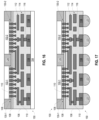
- FIGS. 5 - 8 are top views of example direct bonding interfaces, in accordance with various embodiments.
- FIGS. 9 - 12 are side, cross-sectional views of example direct bonding interfaces, in accordance with various embodiments.
- FIG. 13 is a side, cross-sectional view of an example microelectronic assembly including direct bonding, in accordance with various embodiments.
- FIGS. 14 - 17 are side, cross-sectional views of example stages in the manufacture of a portion of the microelectronic assembly of FIGS. 1 and 2 , in accordance with various embodiments.
- FIGS. 18 - 20 are side, cross-sectional views of example microelectronic assemblies including direct bonding, in accordance with various embodiments.
- FIGS. 21 - 22 are top views of example direct bonding interfaces, in accordance with various embodiments.
- FIG. 23 is a side, cross-sectional view of an example microelectronic assembly including direct bonding regions with multiple subregions, in accordance with various embodiments.
- FIGS. 24 - 25 are top views of example direct bonding interfaces with multiple subregions, in accordance with various embodiments.
- FIGS. 26 A- 26 B are side, cross-sectional and top views, respectively, of a microelectronic assembly including dummy metal traces in and around the direct bonding regions, in accordance with various embodiments.
- FIGS. 27 - 28 are side, cross-sectional views of example microelectronic assemblies including direct bonding, in accordance with various embodiments.
- FIGS. 29 A- 29 B are side, cross-sectional and top views, respectively, of an example portion of a microelectronic assembly with power/ground planes in a direct bonding region, in accordance with various embodiments.
- FIGS. 30 - 31 are top views of example portions of microelectronic assemblies with power/ground planes in the direct bonding regions, in accordance with various embodiments.
- FIG. 32 is a side, cross-sectional view of an example portion of a microelectronic assembly with cantilevered power/ground planes in a direct bonding region, in accordance with various embodiments.
- FIG. 33 is a top view of a wafer and dies that may be included in a microelectronic component in accordance with any of the embodiments disclosed herein.
- FIG. 34 is a side, cross-sectional view of an integrated circuit (IC) device that may be included in a microelectronic component in accordance with any of the embodiments disclosed herein.
- IC integrated circuit
- FIG. 35 is a side, cross-sectional view of an IC device assembly that may include a microelectronic assembly in accordance with any of the embodiments disclosed herein.
- FIG. 36 is a block diagram of an example electrical device that may include a microelectronic assembly in accordance with any of the embodiments disclosed herein.
- a microelectronic assembly may include a first microelectronic component and a second microelectronic component coupled to the first microelectronic component by a direct bonding region, wherein the direct bonding region includes a first subregion and a second subregion, and the first subregion has a greater metal density than the second subregion.
- a microelectronic assembly may include a first microelectronic component and a second microelectronic component coupled to the first microelectronic component by a direct bonding region, wherein the direct bonding region includes a first metal contact and a second metal contact, the first metal contact has a larger area than the second metal contact, and the first metal contact is electrically coupled to a power/ground plane of the first microelectronic component.
- the phrases “A and/or B” and “A or B” mean (A), (B), or (A and B).
- the phrases “A, B, and/or C” and “A, B, or C” mean (A), (B), (C), (A and B), (A and C), (B and C), or (A, B, and C).
- the drawings are not necessarily to scale. Although many of the drawings illustrate rectilinear structures with flat walls and right-angle corners, this is simply for ease of illustration, and actual devices made using these techniques will exhibit rounded corners, surface roughness, and other features.
- a dielectric material may include one or more dielectric materials.
- a “conductive contact” may refer to a portion of conductive material (e.g., metal) serving as an electrical interface between different components; conductive contacts may be recessed in, flush with, or extending away from a surface of a component, and may take any suitable form (e.g., a conductive pad or socket, or portion of a conductive line or via).
- conductive material e.g., metal
- conductive contacts may be recessed in, flush with, or extending away from a surface of a component, and may take any suitable form (e.g., a conductive pad or socket, or portion of a conductive line or via).
- FIG. 1 is a side, cross-sectional view of a microelectronic assembly 100 , in accordance with various embodiments.
- a number of elements are illustrated in FIG. 1 as included in the microelectronic assembly 100 , but a number of these elements may not be present in a microelectronic assembly 100 .
- the heat transfer structure 152 , the thermal interface material (TIM) 154 , the mold material 126 , the microelectronic component 102 - 2 , the underfill material 138 , and/or the support component 182 may not be included.
- FIG. 1 illustrates a number of elements that are omitted from subsequent drawings for ease of illustration, but may be included in any of the microelectronic assemblies 100 disclosed herein.
- Examples of such elements include the heat transfer structure 152 , the TIM 154 , the mold material 126 , the microelectronic component 102 - 2 , the underfill material 138 , and/or the support component 182 .
- Many of the elements of the microelectronic assembly 100 of FIG. 1 are included in other ones of the accompanying drawings; the discussion of these elements is not repeated when discussing these FIGS., and any of these elements may take any of the forms disclosed herein.
- individual ones of the microelectronic assemblies 100 disclosed herein may serve as a system-in-package (SiP) in which multiple microelectronic components 102 having different functionality are included.
- the microelectronic assembly 100 may be referred to as an SiP.
- the microelectronic assembly 100 may include an interposer 150 coupled to a microelectronic component 102 - 1 by a direct bonding (DB) region 130 - 1 .
- the DB region 130 - 1 may include a DB interface 180 - 1 A at the top surface of the interposer 150 , with the DB interface 180 - 1 A including a set of conductive DB contacts 110 and a DB dielectric 108 around the DB contacts 110 of the DB interface 180 - 1 A.
- the DB region 130 - 1 may also include a DB interface 180 - 1 B at the bottom surface of the microelectronic component 102 - 1 , with the DB interface 180 - 1 B including a set of DB contacts 110 and a DB dielectric 108 around the DB contacts 110 of the DB interface 180 - 1 B.
- the DB contacts 110 of the DB interface 180 - 1 A of the interposer 150 may align with the DB contacts 110 of the DB interface 180 - 1 B of the microelectronic component 102 - 1 so that, in the microelectronic assembly 100 , the DB contacts 110 of the microelectronic component 102 - 1 are in contact with the DB contacts 110 of the interposer 150 .
- the DB interface 180 - 1 A of the interposer 150 may be bonded (e.g., electrically and mechanically) with the DB interface 180 - 1 B of the microelectronic component 102 - 1 to form the DB region 130 - 1 coupling the interposer 150 and the microelectronic component 102 - 1 , as discussed further below.
- the DB regions 130 disclosed herein may include two complementary DB interfaces 180 bonded together; for ease of illustration, many of the subsequent drawings may omit the identification of the DB interfaces 180 to improve the clarity of the drawings.
- direct bonding is used to include metal-to-metal bonding techniques (e.g., copper-to-copper bonding, or other techniques in which the DB contacts 110 of opposing DB interfaces 180 are brought into contact first, then subject to heat and compression) and hybrid bonding techniques (e.g., techniques in which the DB dielectric 108 of opposing DB interfaces 180 are brought into contact first, then subject to heat and sometimes compression, or techniques in which the DB contacts 110 and the DB dielectric 108 of opposing DB interfaces 180 are brought into contact substantially simultaneously, then subject to heat and compression).
- metal-to-metal bonding techniques e.g., copper-to-copper bonding, or other techniques in which the DB contacts 110 of opposing DB interfaces 180 are brought into contact first, then subject to heat and compression
- hybrid bonding techniques e.g., techniques in which the DB dielectric 108 of opposing DB interfaces 180 are brought into contact first, then subject to heat and sometimes compression, or techniques in which the DB contacts 110 and
- the DB contacts 110 and the DB dielectric 108 at one DB interface 180 are brought into contact with the DB contacts 110 and the DB dielectric 108 at another DB interface 180 , respectively, and elevated pressures and/or temperatures may be applied to cause the contacting DB contacts 110 and/or the contacting DB dielectrics 108 to bond.
- this bond may be achieved without the use of intervening solder or an anisotropic conductive material, while in some other embodiments, a thin cap of solder may be used in a DB interconnect to accommodate planarity, and this solder may become an intermetallic compound (IMC) in the DB region 130 during processing.
- IMC intermetallic compound
- DB interconnects may be capable of reliably conducting a higher current than other types of interconnects; for example, some conventional solder interconnects may form large volumes of brittle IMGs when current flows, and the maximum current provided through such interconnects may be constrained to mitigate mechanical failure.
- a DB dielectric 108 may include one or more dielectric materials, such as one or more inorganic dielectric materials.
- a DB dielectric 108 may include silicon and nitrogen (e.g., in the form of silicon nitride); silicon and oxygen (e.g., in the form of silicon oxide); silicon, carbon, and nitrogen (e.g., in the form of silicon carbon nitride); carbon and oxygen (e.g., in the form of a carbon-doped oxide); silicon, oxygen, and nitrogen (e.g., in the form of silicon oxynitride); aluminum and oxygen (e.g., in the form of aluminum oxide); titanium and oxygen (e.g., in the form of titanium oxide); hafnium and oxygen (e.g., in the form of hafnium oxide); silicon, oxygen, carbon, and hydrogen (e.g., in the form of tetraethyl orthosilicate (TEOS)); zirconium and oxygen (e.g., in the form of zircon
- a DB contact 110 may include a pillar, a pad, or other structure.
- the DB contacts 110 although depicted in the accompanying drawings in the same manner at both DB interfaces 180 of a DB region 130 , may have a same structure at both DB interfaces 180 , or the DB contacts 110 at different DB interfaces 180 may have different structures.
- a DB contact 110 in one DB interface 180 may include a metal pillar (e.g., a copper pillar), and a complementary DB contact 110 in a complementary DB interface 180 may include a metal pad (e.g., a copper pad) recessed in a dielectric.
- a DB contact 110 may include any one or more conductive materials, such as copper, manganese, titanium, gold, silver, palladium, nickel, copper and aluminum (e.g., in the form of a copper aluminum alloy), tantalum (e.g., tantalum metal, or tantalum and nitrogen in the form of tantalum nitride), cobalt, cobalt and iron (e.g., in the form of a cobalt iron alloy), or any alloys of any of the foregoing (e.g., copper, manganese, and nickel in the form of manganin).
- conductive materials such as copper, manganese, titanium, gold, silver, palladium, nickel, copper and aluminum (e.g., in the form of a copper aluminum alloy), tantalum (e.g., tantalum metal, or tantalum and nitrogen in the form of tantalum nitride), cobalt, cobalt and iron (e.g., in the form of a cobalt iron alloy), or any alloy
- the DB dielectric 108 and the DB contacts 110 of a DB interface 180 may be manufactured using low-temperature deposition techniques (e.g., techniques in which deposition occurs at temperatures below 250 degrees Celsius, or below 200 degrees Celsius), such as low-temperature plasma-enhanced chemical vapor deposition (PECVD).
- PECVD low-temperature plasma-enhanced chemical vapor deposition
- FIGS. 1 and 2 also illustrate a microelectronic component 102 - 2 coupled to the interposer 150 by a DB region 130 - 2 (via the DB interfaces 180 - 2 A and 180 - 2 B, as shown in FIG. 2 ).
- FIG. 1 depicts a particular number of microelectronic components 102 coupled to the interposer 150 by DB regions 130 , this number and arrangement are simply illustrative, and a microelectronic assembly 100 may include any desired number and arrangement of microelectronic components 102 coupled to an interposer 150 by DB regions 130 .
- DB dielectric 108 may have different materials and/or structures (e.g., in accordance with any of the embodiments discussed below with reference to FIG. 3 ).
- DB contacts 110 may have different materials and/or structures (e.g., in accordance with any of the embodiments discussed below with reference to FIG. 4 ).
- the interposer 150 may include an insulating material 106 (e.g., one or more dielectric materials formed in multiple layers, as known in the art) and one or more conductive pathways 112 through the insulating material 106 (e.g., including lines 114 and/or vias 116 , as shown).
- the insulating material 106 of the interposer 150 may be an organic material, such as polyimide or polybenzoxazole, or may include an organic polymer matrix (e.g., epoxide) with a filler material (that may be inorganic).
- the interposer 150 may be referred to as an “organic interposer.”
- the insulating material 106 of an interposer 150 may be provided in multiple layers of organic buildup film.
- Organic interposers 150 may be less expensive to manufacture than semiconductor- or glass-based interposers, and may have electrical performance advantages due to the low dielectric constants of organic insulating materials 106 and the thicker lines that may be used (allowing for improved power delivery, signaling, and potential thermal benefits).
- Organic interposers 150 may also have larger footprints than can be achieved for semiconductor-based interposers, which are limited by the size of the reticle used for patterning.
- organic interposers 150 may be subject to less restrictive design rules than those that constrain semiconductor- or glass-based interposers, allowing for the use of design features such as non-Manhattan routing (e.g., not being restricted to using one layer for horizontal interconnects and another layer for vertical interconnects) and the avoidance of through-substrate vias (TSVs) such as through-silicon vias or through-glass vias (which may be limited in the achievable pitch, and may result in less desirable power delivery and signaling performance).
- TSVs through-substrate vias
- Conventional integrated circuit packages including an organic interposer have been limited to solder-based attach technologies, which may have a lower limit on the achievable pitch that precludes the use of conventional solder-based interconnects to achieve the fine pitches desired for next generation devices.
- Utilizing an organic interposer 150 in a microelectronic assembly 100 with direct bonding may leverage these advantages of organic interposers in combination with the ultra-fine pitch (e.g., the pitch 128 discussed below) achievable by direct bonding (and previously only achievable when using semiconductor-based interposers), and thus may support the design and fabrication of large and sophisticated die complexes that can achieve packaged system competition performance and capabilities not enabled by conventional approaches.
- the ultra-fine pitch e.g., the pitch 128 discussed below
- the insulating material 106 of the interposer 150 may include a fire retardant grade 4 material (FR-4), bismaleimide triazine (BT) resin, or low-k or ultra low-k dielectric (e.g., carbon-doped dielectrics, fluorine-doped dielectrics, and porous dielectrics).
- FR-4 fire retardant grade 4 material
- BT bismaleimide triazine
- ultra low-k dielectric e.g., carbon-doped dielectrics, fluorine-doped dielectrics, and porous dielectrics.
- the interposer 150 may include FR-4, and the conductive pathways 112 in the interposer 150 may be formed by patterned sheets of copper separated by buildup layers of the FR-4.
- the interposer 150 may be referred to as a “package substrate” or a “circuit board.”
- one or more of the conductive pathways 112 in the interposer 150 may extend between a conductive contact at the top surface of the interposer 150 (e.g., one of the DB contacts 110 ) and a conductive contact 118 at the bottom surface of the interposer 150 . In some embodiments, one or more of the conductive pathways 112 in the interposer 150 may extend between different conductive contacts at the top surface of the interposer 150 (e.g., between different DB contacts 110 potentially in different DB regions 130 , as discussed further below). In some embodiments, one or more of the conductive pathways 112 in the interposer 150 may extend between different conductive contacts 118 at the bottom surface of the interposer 150 .
- an interposer 150 may only include conductive pathways 112 , and may not contain active or passive circuitry. In other embodiments, an interposer 150 may include active or passive circuitry (e.g., transistors, diodes, resistors, inductors, and capacitors, among others). In some embodiments, an interposer 150 may include one or more device layers including transistors.
- active or passive circuitry e.g., transistors, diodes, resistors, inductors, and capacitors, among others.
- an interposer 150 may include one or more device layers including transistors.
- FIGS. 1 and 2 illustrate a specific number and arrangement of conductive pathways 112 in the interposer 150 , these are simply illustrative, and any suitable number and arrangement may be used.
- the conductive pathways 112 disclosed herein e.g., including lines 114 and/or vias 116
- a microelectronic component 102 may include an IC die (packaged or unpackaged) or a stack of IC dies (e.g., a high-bandwidth memory dies stack).
- the insulating material of a microelectronic component 102 may include silicon dioxide, silicon nitride, oxynitride, polyimide materials, glass-reinforced epoxy matrix materials, or a low-k or ultra low-k dielectric (e.g., carbon-doped dielectrics, fluorine-doped dielectrics, porous dielectrics, organic polymeric dielectrics, photo-imageable dielectrics, and/or benzocyclobutene-based polymers).
- the insulating material of a microelectronic component 102 may include a semiconductor material, such as silicon, germanium, or a III-V material (e.g., gallium nitride), and one or more additional materials.
- an insulating material of a microelectronic component 102 may include silicon oxide or silicon nitride.
- the conductive pathways in a microelectronic component 102 may include conductive lines and/or conductive vias, and may connect any of the conductive contacts in the microelectronic component 102 in any suitable manner (e.g., connecting multiple conductive contacts on a same surface or on different surfaces of the microelectronic component 102 ).
- a microelectronic component 102 may include active and/or passive circuitry (e.g., transistors, diodes, resistors, inductors, and capacitors, among others).
- a microelectronic component 102 may include one or more device layers including transistors.
- power and/or ground signals may be routed through the interposer 150 and to/from a microelectronic component 102 through a DB region 130 (and further through intervening microelectronic components 102 ).
- a microelectronic component 102 may take the form of any of the embodiments of the interposer 150 herein.
- the microelectronic components 102 of the microelectronic assembly 100 of FIG. 1 are single-sided components (in the sense that an individual microelectronic component 102 only has conductive contacts (e.g., DB contacts 110 ) on a single surface of the individual microelectronic component 102 ), in some embodiments, a microelectronic component 102 may be a double-sided (or “multi-level,” or “omni-directional”) component with conductive contacts on multiple surfaces of the component. Some particular examples of double-sided microelectronic components 102 are discussed below with reference to FIG. 28 .
- the microelectronic assembly 100 of FIG. 1 also includes a support component 182 coupled to the interposer 150 .
- a support component 182 coupled to the interposer 150 .
- the support component 182 includes conductive contacts 118 that are electrically coupled to complementary conductive contacts 118 of the interposer 150 by intervening solder 120 (e.g., solder balls in a ball grid array (BGA) arrangement), but any suitable interconnect structures may be used (e.g., pins in a pin grid array arrangement, lands in a land grid array arrangement, pillars, pads and pillars, etc.).
- solder 120 e.g., solder balls in a ball grid array (BGA) arrangement
- BGA ball grid array
- the solder 120 utilized in the microelectronic assemblies 100 disclosed herein may include any suitable materials, such as lead/tin, tin/bismuth, eutectic tin/silver, ternary tin/silver/copper, eutectic tin/copper, tin/nickel/copper, tin/bismuth/copper, tin/indium/copper, tin/zinc/indium/bismuth, or other alloys.
- the couplings between the interposer 150 and the support component 182 may be referred to as second-level interconnects (SLI) or multi-level interconnects (MLI).
- the support component 182 may be a package substrate (e.g., may be manufactured using PCB processes, as discussed above). In some embodiments, the support component 182 may be a circuit board (e.g., a motherboard), and may have other components attached to it (not shown). The support component 182 may include conductive pathways and other conductive contacts (not shown) for routing power, ground, and signals through the support component 182 , as known in the art. In some embodiments, the support component 182 may include another IC package, an interposer, or any other suitable component. An underfill material 138 may be disposed around the solder 120 coupling the interposer 150 to the support component 182 . In some embodiments, the underfill material 138 may include an epoxy material.
- the support component 182 may be a lower density component, while the interposer 150 and/or the microelectronic components 102 may be higher density components.
- the term “lower density” and “higher density” are relative terms indicating that the conductive pathways (e.g., including conductive lines and conductive vias) in a lower density component are larger and/or have a greater pitch than the conductive pathways in a higher density component.
- a microelectronic component 102 may be a higher density component
- an interposer 150 may be a lower density component.
- a higher density component may be manufactured using a dual damascene or single damascene process (e.g., when the higher density component is a die), while a lower density component may be manufactured using a semi-additive or modified semi-additive process (with small vertical interconnect features formed by advanced laser or lithography processes) (e.g., when the lower density component is a package substrate or an interposer).
- a higher density component may be manufactured using a semi-additive or modified semi-additive process (e.g., when the higher density component is a package substrate or an interposer), while a lower density component may be manufactured using a semi-additive or a subtractive process (using etch chemistry to remove areas of unwanted metal, and with coarse vertical interconnect features formed by a standard laser process) (e.g., when the lower density component is a PCB).
- a semi-additive or modified semi-additive process e.g., when the higher density component is a package substrate or an interposer
- a lower density component may be manufactured using a semi-additive or a subtractive process (using etch chemistry to remove areas of unwanted metal, and with coarse vertical interconnect features formed by a standard laser process) (e.g., when the lower density component is a PCB).
- the microelectronic assembly 100 of FIG. 1 may also include a mold material 126 .
- the mold material 126 may extend around one or more of the microelectronic components 102 on the interposer 150 .
- the mold material 126 may extend between multiple microelectronic components 102 on the interposer 150 and around the DB regions 130 .
- the mold material 126 may extend above one or more of the microelectronic components 102 on an interposer 150 (not shown).
- the mold material 126 may be an insulating material, such as an appropriate epoxy material.
- the mold material 126 may be selected to have a coefficient of thermal expansion (CTE) that may mitigate or minimize the stress between the microelectronic components 102 and the interposer 150 arising from uneven thermal expansion in the microelectronic assembly 100 .
- CTE of the mold material 126 may have a value that is intermediate to the CTE of the interposer 150 (e.g., the CTE of the insulating material 106 of the interposer 150 ) and a CTE of the microelectronic components 102 .
- the mold material 126 used in a microelectronic assembly 100 may be selected at least in part for its thermal properties.
- one or more mold materials 126 used in a microelectronic assembly 100 may have low thermal conductivity (e.g., conventional mold compounds) to retard heat transfer, or may have high thermal conductivity (e.g., mold materials including metal or ceramic particles with high thermal conductivity, such as copper, silver, diamond, silicon carbide, aluminum nitride, and boron nitride, among others) to facilitate heat transfer.
- low thermal conductivity e.g., conventional mold compounds
- high thermal conductivity e.g., mold materials including metal or ceramic particles with high thermal conductivity, such as copper, silver, diamond, silicon carbide, aluminum nitride, and boron nitride, among others
- Any of the mold materials 126 referred to herein may include one or more different materials with different material compositions.
- the microelectronic assembly 100 of FIG. 1 may also include a TIM 154 .
- the TIM 154 may include a thermally conductive material (e.g., metal particles) in a polymer or other binder.
- the TIM 154 may be a thermal interface material paste or a thermally conductive epoxy (which may be a fluid when applied and may harden upon curing, as known in the art).
- the TIM 154 may provide a path for heat generated by the microelectronic components 102 to readily flow to the heat transfer structure 152 , where it may be spread and/or dissipated.
- the TIM 154 e.g., a solder TIM
- the microelectronic assembly 100 of FIG. 1 may also include a heat transfer structure 152 .
- the heat transfer structure 152 may be used to move heat away from one or more of the microelectronic components 102 (e.g., so that the heat may be more readily dissipated).
- the heat transfer structure 152 may include any suitable thermally conductive material (e.g., metal, appropriate ceramics, etc.), and may include any suitable features (e.g., a heat spreader, a heat sink including fins, a cold plate, etc.).
- a heat transfer structure 152 may be or may include an integrated heat spreader (IHS).
- the thickness 184 of the interposer 150 may be between 20 microns and 200 microns.
- the thickness 188 of a DB region 130 may be between 50 nanometers and 5 microns.
- a thickness 190 of a microelectronic component 102 may be between 5 microns and 800 microns.
- a pitch 128 of the DB contacts 110 in a DB region 130 may be less than 20 microns (e.g., between 0.1 microns and 20 microns).
- FIGS. 3 - 32 illustrate additional example microelectronic assemblies 100 and components thereof. Any of the features discussed with reference to any of FIGS. 3 - 32 herein may be combined with any other features to form a microelectronic assembly 100 or component thereof.
- FIG. 4 illustrates an embodiment of a DB interface 180 in which a DB contact 110 includes multiple different material portions
- FIG. 9 illustrates an embodiment of a DB interface 180 in which a liner material 132 is present between a DB contact 110 and the adjacent DB dielectric 108 .
- a DB interface 180 in accordance with the present disclosure, has DB contacts 110 with multiple different material portions and a liner material 132 between DB contacts 110 and adjacent DB dielectric 108 .
- This particular combination is simply an example, and any combination may be used.
- a DB dielectric 108 may include one or more materials arranged in any desired manner.
- FIG. 3 illustrates a DB interface 180 (which may be part of an interposer 150 or a microelectronic component 102 ) that includes DB dielectric 108 around DB contacts 110 .
- the DB dielectric 108 may include a first portion 108 A and a second portion 108 B, with the second portion 108 B between the first portion 108 A and the bonding surface of the DB interface 180 .
- the first portion 108 A and the second portion 108 B may have different material compositions.
- the first portion 108 A may include silicon and oxygen (e.g., in the form of silicon oxide), and the second portion 108 B may include silicon, oxygen, carbon, and nitrogen (e.g., in the form of silicon oxycarbonitride).
- the thickness 190 A of the first portion 108 A may be greater than the thickness 190 B of the second portion 108 B.
- the thickness 190 B may be less than 5 nanometers (e.g., less than 3 nanometers), while the thickness 190 A may be greater than 5 nanometers (e.g., between 50 nanometers and 5 microns).
- the first portion 108 A may be referred to as a “bulk” material and the second portion 108 B may be referred to as an “interface” material of the DB dielectric 108 .
- FIG. 3 illustrates an embodiment in which the DB dielectric 108 includes two portions, a DB dielectric 108 may include more than two portions (e.g., arranged in layers parallel to the bonding surface of the DB interface 180 ).
- the first portion 110 A may include copper, and the second portion 110 B may include a noble metal (e.g., silver or gold); in such embodiments, the second portion 110 B may serve to improve the resistance of the DB contacts 110 to corrosion.
- the thickness 192 A of the first portion 110 A may be greater than the thickness 192 B of the second portion 110 B.
- the thickness 192 B may be less than 5 nanometers, while the thickness 192 A may be greater than 50 nanometers.
- the first portion 110 A may be referred to as a “bulk” material and the second portion 110 B may be referred to as an “interface” material of the DB contacts 110 .
- a DB contact 110 may include more than two portions (e.g., arranged in layers parallel to the bonding surface of the DB interface 180 ).
- a DB interface 180 may include a DB dielectric 108 with multiple portions and a DB contact 110 with multiple portions.
- FIGS. 5 - 8 are top views of various arrangements of DB contacts 110 in a DB dielectric 108 of a DB interface 180 .
- the DB contacts 110 have rectangular (e.g., square) footprints and are arranged in a rectangular array.
- the DB contacts 110 have cross-shaped footprints and are arranged in a triangular array.
- FIG. 5 the DB contacts 110 have rectangular (e.g., square) footprints and are arranged in a rectangular array.
- the DB contacts 110 have cross-shaped footprints and are arranged in a triangular array.
- the DB contacts 110 are arranged in a rectangular array, and alternating rows of the DB contacts 110 have cross-shaped footprints and triangular footprints.
- the DB contacts 110 are arranged in a rectangular array, the DB contacts 110 have circular footprints, and the diameters of the footprints of the DB contacts 110 vary in a checkerboard pattern.
- DB contacts 110 included in a DB interface 180 may have any suitable combination of these and other footprint shapes, sizes, and arrangements (e.g., hexagonal arrays, oval footprints, etc.).
- DB contacts 110 in a DB interface 180 may have footprints shaped as convex polygons (e.g., squares, rectangles, octagons, cross shapes, etc.) or circles.
- a liner material may be present between a DB contact 110 and the adjacent DB dielectric 108 .
- FIG. 9 illustrates a portion of an interposer 150 and its DB interface 180 .
- a liner material 132 is present between the DB contacts 110 and the adjacent DB dielectric 108 .
- the liner material 132 may serve as a diffusion barrier (e.g., to limit diffusion between the DB contacts 110 and the adjacent DB dielectric 108 , such as the copper diffusion that may occur when the DB contacts 110 include copper and the DB dielectric 108 includes silicon oxide) and/or as an adhesion promoter (e.g., to improve the strength of the mechanical interface between the DB contacts 110 and the adjacent DB dielectric 108 ).
- the liner material 132 may not be present around the vias 116 and/or the lines 114 through the insulating material 106 of the interposer 150 .
- the liner material 132 may also be present around the vias 116 and/or the lines 114 ; such an embodiment is illustrated in FIG. 10 . In some embodiments, a liner material 132 may only be present around the vias 116 and/or the lines 114 , but not around the DB contacts 110 (not shown).
- the liner material 132 may be a conductive material (e.g., may include cobalt, ruthenium, or tantalum and nitrogen (e.g., in the form of tantalum nitride)), or a non-conductive material (e.g., silicon and nitrogen (e.g., in the form of silicon nitride), or diamond-like carbon).
- the liner material 132 may be a non-conductive material. In still other embodiments, no liner material 132 may be present in an interposer 150 . Although various embodiments of the use of liner material 132 are depicted in FIGS. 9 and 10 and discussed with respect to their presence in an interposer 150 , this is simply for ease of illustration, and DB interfaces 180 of microelectronic components 102 may also include liner materials 132 (e.g., only around the DB contacts 110 , and/or around lines and vias in a metallization stack of the microelectronic component 102 ).
- lithographic via techniques may be used to form one or more layers of metallization in an interposer 150 (e.g., in an organic interposer 150 ) or a microelectronic component 102 .
- FIG. 11 illustrates a portion of an interposer 150 and its DB interface 180 .
- three different layers of insulating material 106 are shown (labeled as 106 A, 106 B, and 106 C).
- vias 116 may be patterned using lithographic techniques (e.g., “zero-misalignment” techniques) so that their side faces are aligned with side faces of the lines 114 on which they land.
- lithographic techniques e.g., “zero-misalignment” techniques
- vias 116 may be patterned using conventional techniques and the side faces of the vias 116 may not align with side faces of the lines 114 on which they land.
- a via 116 formed lithographically may have any desired footprint (e.g., a non-circular footprint).
- the DB contacts 110 may be “pads” in conductive contact with the vias 116 of the layer 106 A.
- the use of lithographic via techniques in the formation of the DB interface 180 may result in an extremely flat DB interface 180 due to the planarization (e.g., chemical mechanical polishing) operations performed during lithographic via fabrication, and flat DB interfaces 180 may more reliably form direct bonds than more “uneven” DB interfaces 180 .
- the use of lithographic via techniques to form the DB contacts 110 of a DB interface 180 may support a mechanically and electrically reliable DB region 130 .
- lithographic via techniques may be used to form the DB contacts 110 in a DB interface 180 of an interposer 150 (e.g., in an organic interposer 150 ) or a microelectronic component 102 .
- FIG. 12 illustrates a portion of an interposer 150 and its DB interface 180 .
- a DB contact 110 includes a via 116 and a line 114 on which the via 116 lands; these vias 116 may be patterned using lithographic techniques (e.g., so that the side faces of the vias 116 are aligned with side faces of the lines 114 on which they land).
- the DB dielectric 108 may contact the vias 116 and lines 114 of the DB contacts 110 , as shown.
- Metallization in the insulating material 106 may be patterned using lithographic techniques or conventional techniques. Although various embodiments of vias 116 /lines 114 are depicted in FIGS. 11 and 12 and discussed with respect to their presence in an interposer 150 , this is simply for ease of illustration, and DB interfaces 180 of microelectronic components 102 may also include lithographically patterned vias 116 /lines 114 in the DB interfaces 180 and/or the other metallization.
- the DB contacts 110 are shown as pads in contact with vias 116 in the underlying insulating material 106 .
- the DB contacts 110 may be vias themselves.
- FIG. 13 illustrates an embodiment in which the DB contacts 110 are vias in contact with pads in the insulating material 106 ; as shown, the DB contacts 110 may be narrower than the pads with which they are in contact.
- FIGS. 14 - 17 are side, cross-sectional views of example stages in the manufacture of a portion of the microelectronic assembly 100 of FIGS. 1 and 2 , in accordance with various embodiments.
- FIGS. 14 - 17 may be illustrated with reference to particular embodiments of the microelectronic assemblies 100 disclosed herein, the manufacturing methods discussed with reference to FIGS. 14 - 17 may be used to form any suitable microelectronic assemblies 100 . Operations are illustrated once each and in a particular order in FIGS.
- the operations may be reordered and/or repeated as desired (e.g., with different operations performed in parallel when manufacturing multiple microelectronic assemblies 100 simultaneously).
- the manufacturing processes discussed below with reference to FIGS. 14 - 17 may be particularly advantageous when the interposer 150 is an organic interposer, and may also be advantageous for glass-based or semiconductor-based interposers (e.g., glass-based or silicon-based interposers in which the underlying glass or silicon wafer has already been thinned, and TSVs formed, before any direct bonding operations).
- any suitable manufacturing processes may be used to manufacture any of the microelectronic assemblies 100 disclosed herein.
- FIG. 14 illustrates an assembly including an interposer 150 mounted on a carrier 104 .
- the interposer 150 includes two exposed DB interfaces 180 - 1 and 180 - 2 .
- the carrier 104 may include any suitable material, and in some embodiments, may include a semiconductor wafer (e.g., a silicon wafer) or glass (e.g., a glass panel).
- the interposer 150 is an organic interposer, the interposer 150 may be advantageously manufactured on the carrier 104 , which may provide a mechanically stable surface on which the layers of the interposer 150 may be formed.
- FIG. 15 illustrates an assembly subsequent to direct bonding microelectronic components 102 - 1 and 102 - 2 to the interposer 150 /carrier 104 of FIG. 14 .
- DB interfaces 180 (not labeled) of the microelectronic components 102 may be brought into contact with the DB interfaces 180 of the interposer 150 , and heat and/or pressure may be applied to bond the contacting DB interfaces 180 to form DB regions 130 (with DB regions 130 - 1 and 130 - 2 corresponding to the DB interfaces 180 - 1 and 180 - 2 , respectively).
- FIG. 16 illustrates an assembly subsequent to providing a mold material 126 around the microelectronic components 102 and on the surface of the interposer 150 of the assembly of FIG. 15 .
- the mold material 126 may extend above and remain above the microelectronic components 102 , while in other embodiments, the mold material 126 may be polished back to expose the top surfaces of the microelectronic components 102 , as shown.
- FIG. 17 illustrates an assembly subsequent to removing the carrier 104 from the assembly of FIG. 16 , and providing solder 120 on the newly exposed conductive contacts 118 .
- the assembly of FIG. 17 may itself be a microelectronic assembly 100 , as shown. Further manufacturing operations may be performed on the microelectronic assembly 100 of FIG. 17 to form other microelectronic assemblies 100 ; for example, the solder 120 may be used to couple the microelectronic assembly 100 of FIG. 17 to a support component 182 , and a TIM 154 and heat transfer structure 152 may be provided on the top surface of the microelectronic assembly 100 of FIG. 17 , forming the microelectronic assembly 100 of FIGS. 1 and 2 .
- Different DB regions 130 in a microelectronic assembly 100 may include different DB dielectrics 108 .
- FIG. 18 illustrates a microelectronic assembly 100 in which a DB region 130 - 1 includes a DB dielectric 108 - 1 and a DB region 130 - 2 includes a different DB dielectric 108 - 2 .
- the DB dielectrics 108 - 1 and 108 - 2 may differ in their material composition and/or their structure.
- DB dielectrics 108 in different DB regions 130 may be selected to have different thermal conductivities so as to facilitate and/or limit heat transfer between the interposer 150 and the microelectronic components 102 .
- the DB dielectric 108 - 1 may have a higher thermal conductivity than the DB dielectric 108 - 2 , resulting in greater heat transfer between the microelectronic component 102 - 1 and the interposer 150 than between the microelectronic component 102 - 2 and the interposer 150 .
- the DB dielectric 108 - 1 may include silicon and nitrogen (e.g., in the form of silicon nitride) and the DB dielectric 108 - 2 may include silicon and oxygen (e.g., in the form of silicon oxide); silicon nitride may have a higher thermal conductivity than silicon oxide, and thus the use of silicon nitride as the DB dielectric 108 - 1 may enhance local heat transfer from the microelectronic component 102 - 1 to the interposer 150 , while the use of silicon oxide as the DB dielectric 108 - 2 may mitigate thermal cross-talk through the interposer 150 between the microelectronic component 102 - 1 and the microelectronic component 102 - 2 .
- the density of the DB contacts 110 may differ between different DB regions 130 .
- this different density may be due to one DB region 130 requiring fewer electrical pathways than another DB region 130 .
- this differing density may be used to enhance or suppress heat transfer, with greater density of DB contacts 110 (and therefore a higher proportion of thermally conductive metal) being used to enhance heat transfer and lesser density of DB contacts 110 (and therefore a lower portion of thermally conductive metal) being used to suppress heat transfer.
- FIG. 19 illustrates an embodiment in which the density of DB contacts 110 is greater in the DB region 130 - 1 than in the DB region 130 - 2 to enhance heat transfer between the microelectronic component 102 - 1 and the interposer 150 and to reduce heat transfer between the microelectronic component 102 - 2 and the interposer 150 .
- FIG. 19 illustrates different densities of DB contacts 110 being accompanied by the use of different DB dielectrics 108 in different DB regions 130 , but in some embodiments, two DB regions 130 may have different densities of DB contacts 110 while having DB dielectrics 108 with the same material composition.
- FIG. 20 illustrates another embodiment of a microelectronic assembly 100 in which, like the embodiment of FIG. 19 , the density of DB contacts 110 is greater in the DB region 130 - 1 than in the DB region 130 - 2 to enhance heat transfer between the microelectronic component 102 - 1 and the interposer 150 and to reduce heat transfer between the microelectronic component 102 - 2 and the interposer 150 .
- the density of DB contacts 110 is greater in the DB region 130 - 1 than in the DB region 130 - 2 to enhance heat transfer between the microelectronic component 102 - 1 and the interposer 150 and to reduce heat transfer between the microelectronic component 102 - 2 and the interposer 150 .
- the size (e.g., the area of the footprint) of the DB contacts 110 of the DB region 130 - 1 may be the same as the size of the DB contacts 110 of the DB region 130 - 2 ; the DB region 130 - 1 may simply include more DB contacts 110 than the DB region 130 - 2 .
- the size (e.g., the area of the footprint) of the DB contacts 110 of the DB region 130 - 1 may be greater than the size of the DB contacts 110 of the DB region 130 - 2 ; the number of DB contacts 110 of the DB region 130 - 1 may be the same as, greater than, or less than the number of DB contacts 110 of the DB region 130 - 2 .
- FIG. 21 is a top view of a DB interface 180 that may correspond to the DB region 130 - 1 of the microelectronic assembly 100 of FIG. 20
- FIG. 22 is a top view of a DB interface 180 that may correspond to the DB region 130 - 2 of the microelectronic assembly 100 of FIG. 20
- the DB contacts 110 may have large rectangular footprints and may be closely spaced relative to the DB contacts 110 of FIG. 22 , which may have smaller circular footprints and may be sparsely distributed.
- DB contacts 110 may be used in different DB regions 130 of a microelectronic assembly 100 (e.g., to achieve desired thermal properties, or for other purposes); such configurability may not be achievable using other attach technologies, such as solder attach, which conventionally require significant uniformity and regularity in contact location and size in order to achieve reliable attachment.
- a single DB region 130 may have multiple subregions with different metal density; such embodiments may be advantageous for achieving desired thermal transfer between different portions of a microelectronic component 102 and an interposer 150 or microelectronic component 102 .
- some portions of a microelectronic component 102 may generate more heat than other regions (e.g., a central processing unit (CPU) may have high power areas, such as matrix multipliers and cache areas, and other lower power areas), and thus within a DB region 130 , subregions proximate to those portions may have greater metal density (e.g., achieved by any suitable combination of size, shape, and distribution of DB contacts 110 ) than subregions of the DB region 130 that are not proximate to those portions.
- CPU central processing unit
- FIG. 23 illustrates a microelectronic assembly 100 in which a DB region 130 - 1 includes a first subregion 130 - 1 A and a second subregion 130 - 1 B, and the metal density of the first subregion 130 - 1 A is greater than the metal density of the second subregion 130 - 1 B.
- the microelectronic assembly 100 of FIG. 23 also illustrates a DB region 130 - 2 that includes a first subregion 130 - 2 A and a second subregion 130 - 2 B, with the metal density of the first subregion 130 - 2 A greater than the metal density of the second subregion 130 - 2 B.
- FIG. 24 is a top view of a DB interface 180 - 1 that may correspond to the DB region 130 - 1 of the microelectronic assembly 100 of FIG. 23
- FIG. 24 is a top view of a DB interface 180 - 2 that may correspond to the DB region 130 - 2 of the microelectronic assembly 100 of FIG. 23 .
- FIG. 24 is a top view of a DB interface 180 - 1 that may correspond to the DB region 130 - 1 of the microelectronic assembly 100 of FIG. 23
- FIG. 24 is a top view of a DB interface 180 - 2 that may correspond to the DB region 130 - 2 of the microelectronic
- a first subregion 180 - 1 A of the DB interface 180 - 1 may correspond to the first subregion 130 - 1 A of the DB region 130 - 1 of FIG. 23
- a second subregion 180 - 1 B of the DB interface 180 - 1 may correspond to the second subregion 130 - 1 B of the DB region 130 - 1 of FIG. 23
- a first subregion 180 - 2 A of the DB interface 180 - 2 may correspond to the first subregion 130 - 2 A of the DB region 130 - 2 of FIG.
- a second subregion 180 - 2 B of the DB interface 180 - 2 may correspond to the second subregion 130 - 2 B of the DB region 130 - 2 of FIG. 23 .
- the second subregion 180 - 1 B may partially wrap around the first subregion 180 - 1 A
- the second subregion 180 - 2 B may wrap around the first subregion 180 - 2 A; these particular arrangements are simply illustrative, and a DB region 130 /DB interface 180 may include any desired arrangement of subregions with different metal densities.
- FIGS. 23 - 25 depict DB regions 130 /DB interfaces 180 that include 2 subregions, this is simply illustrative, and a DB region 130 /DB interface 180 may include two or more subregions, as desired.
- a microelectronic assembly 100 may include features in one or more DB interfaces 180 that may exhibit anisotropic in-plane thermal conductivity, and thus may selectively transfer heat around a surface.
- FIG. 26 depicts a microelectronic assembly 100 in which dummy metal traces 196 (including, e.g., copper and/or any of the materials discussed herein with reference to the DB contacts 110 ) are coplanar with the DB contacts 110 , and may extend from one DB region 130 to another DB region 130 (i.e., between the DB regions 130 - 1 and 130 - 3 of FIG. 26 ).
- FIG. 26 A is a side, cross-sectional view (through the section A-A of FIG.
- FIG. 26 B is a top view of the microelectronic assembly 100 with the mold material 126 and the microelectronic components 102 removed so that the DB contacts 110 and the dummy metal traces 196 are visible; the dashed boxes in FIG. 26 B indicate the footprints of the microelectronic components 102 - 1 , 102 - 2 and 102 - 3 .
- the dummy metal traces 196 may not be coupled to any circuitry in the microelectronic components 102 or in the interposer 150 , but may instead be present as thermal conduits, allowing heat to move along the dummy metal traces 196 in accordance with their pattern; in other embodiments, the dummy metal traces 196 may be coupled to dummy metal lines/vias (e.g., for additional thermal transfer) in the microelectronic components 102 and/or the interposer 150 .
- one or more dummy metal traces 196 may extend between the DB region 130 - 1 (e.g., “under” the microelectronic component 102 - 1 ) and the DB region 130 - 3 (e.g., “under” the microelectronic component 102 - 3 ).
- One or more dummy metal traces 196 may not extend under multiple microelectronic components 102 , but may extend near to multiple microelectronic components 102 and/or under a single microelectronic component 102 ; an example of such a dummy metal trace 196 is shown in FIG.
- the microelectronic component 102 - 1 may be a heat-generating component and the microelectronic component 102 - 3 may be a dummy component (e.g., without active devices, and present to act at least in part as a heat sink); during operation, heat generated by the microelectronic component 102 - 1 may be absorbed by the dummy metal traces 196 and transferred to the microelectronic component 102 - 3 , cooling the microelectronic component 102 - 1 .
- dummy metal traces 196 may extend around a footprint of a microelectronic component 102 that is thermally sensitive (e.g., a memory component, an amplifier, etc.). For example, in the embodiment of FIG. 26 , the dummy metal traces 196 extend around the footprint of the microelectronic component 102 - 2 .
- the DB dielectric 108 - 2 of the DB region 130 - 2 may be selected to have a lower thermal conductivity than the thermal conductivities of the DB dielectric 108 - 1 of the DB region 130 - 1 and the DB dielectric 108 - 3 of the DB region 130 - 3 in order to further thermally insulate the microelectronic component 102 - 2 from heat generated and/or carried by the microelectronic components 102 - 1 and 102 - 3 and the dummy metal traces 196 .
- the dummy metal traces 196 may be part of one or more DB regions 130 (e.g., in the areas in which the dummy metal traces 196 overlap the footprints of the microelectronic components 102 ), and thus some or all of the dummy metal traces 196 may be used for direct bonding.
- the DB dielectric 108 extends outside of the DB regions 130 , covering the remainder of the top surface of the interposer 150 .
- a different material may be disposed at the top surface of the interposer 150 outside of the DB regions 130 .
- FIG. 27 illustrates a microelectronic assembly 100 in which a material 134 , different from the DB dielectrics 108 - 1 and 108 - 2 , is disposed at the top surface of the interposer 150 (e.g., in contact with the mold material 126 ).
- the material 134 may include one or more dielectric materials, such as one or more organic or inorganic dielectric materials.
- the material 134 may include an inorganic dielectric material that includes silicon and nitrogen (e.g., in the form of silicon nitride); silicon and oxygen (e.g., in the form of silicon oxide); or silicon, carbon, and nitrogen (e.g., in the form of silicon carbonitride); or the material 134 may include an organic dielectric material, such as a particle-filled epoxide, a polyimide, a particle-filled polyimide, or poly(p-phenylene- 2 , 6 -benzobisoxazole)) (PBO).
- the material 134 may be a dielectric material, and an additional conductive material (e.g., a metal such as aluminum or copper) may be disposed on the material 134 .
- a microelectronic assembly 100 may include multiple “tiers” of microelectronic components 102 coupled by direct bonding.
- FIG. 28 illustrates a microelectronic assembly 100 in which the microelectronic component 102 - 1 includes two DB interfaces 180 (not labeled) at its top surface, and microelectronic components 102 - 3 and 102 - 4 with their own DB interfaces 180 (not labeled) at the bottom surfaces are coupled to the microelectronic component 102 - 1 via DB regions 130 - 3 and 130 - 4 , respectively.
- the microelectronic component 102 - 2 includes a DB interface 180 (not labeled) at its top surface, and a microelectronic component 102 - 5 with its own DB interface 180 (not labeled) at its bottom surface is coupled to the microelectronic component 102 - 2 via a DB region 130 - 5 .
- the microelectronic assembly 100 of FIG. 28 may thus be described as having two tiers of direct bonded microelectronic components 102 .
- Any microelectronic component 102 disclosed herein may include one or more dies and may have different types of pass-through conductive interconnects, such as copper pillars and TSVs (e.g., through-silicon vias).
- the microelectronic components 102 - 1 and 102 - 2 in the first tier of the microelectronic assembly 100 of FIG. 28 may include conductive structures 194 that extend between the DB regions 130 at their top and bottom surfaces, providing conductive pathways for power, ground, and/or signals to the microelectronic components 102 in the second tier (i.e., the microelectronic components 102 - 3 , 102 - 4 , and 102 - 5 ).
- such a conductive structure 194 may include one or more TSVs, including a conductive material via, such as a metal via, isolated from the surrounding silicon or other semiconductor material by a barrier oxide), such as through-silicon vias when the microelectronic components 102 - 1 and 102 - 2 include silicon substrates or through-glass vias when the microelectronic components 102 - 1 and 102 - 2 include glass substrates.
- the microelectronic components 102 - 1 and 102 - 2 in a first tier may be passive (e.g., including no transistors) or active (e.g., including transistors in the form of memory circuitry and/or power delivery circuitry).
- a mold material 126 may extend up to and may laterally surround the microelectronic components 102 in the second tier, and in some embodiments (not shown), the mold material 126 may cover the top surfaces of the microelectronic components 102 in the second tier. In other embodiments, the top surface of the mold material 126 may be coplanar with the exposed DB interfaces 180 , or recessed below the exposed DB interfaces 180 . In some embodiments, a microelectronic assembly 100 including exposed DB interfaces 180 may have a temporary, removable protective material (e.g., an adhesive material, not shown) on the exposed DB interfaces 180 to protect them until direct bonding operations are performed.
- a temporary, removable protective material e.g., an adhesive material, not shown
- Microelectronic assemblies 100 including multiple tiers of microelectronic components 102 may be formed in a manner discussed above with reference to FIGS. 14 - 17 , with the additional tiers of microelectronic components 102 coupled to the preceding assemblies prior to deposition of the mold material 126 .
- a microelectronic assembly 100 including multiple tiers of microelectronic components 102 may be formed by first assembling the tiers of microelectronic components 102 , and then coupling the assembled tiers to an interposer 150 as discussed above with reference to FIG. 15 .
- a microelectronic assembly 100 may not be limited to two tiers of microelectronic components 102 , but may include three or more tiers, as desired. Further, although the microelectronic components 102 in an individual tier in FIG. 28 are depicted as having a same height, this is simply for ease of illustration, and microelectronic components 102 in any individual tier in a microelectronic assembly 100 may have different heights. Further, not every microelectronic component 102 in a microelectronic assembly 100 may be part of a stack of multiple microelectronic components 102 ; for example, in some variants of the microelectronic assembly 100 of FIG.
- no microelectronic component 102 - 5 may be present on top of the microelectronic component 102 - 2 (and thus the microelectronic component 102 - 2 may not include conductive structures 194 (e.g., may not include TSVs)).
- a microelectronic assembly 100 may include one or more DB interfaces 180 exposed at a surface of the microelectronic assembly 100 .
- various ones of the preceding drawings illustrate DB regions 130 at a single surface of the interposer 150 (e.g., the top surface)
- a microelectronic assembly 100 may include DB regions 130 at multiple surfaces of an interposer 150 .
- a microelectronic component 102 coupled by direct bonding to a bottom surface of the interposer 150 may include conductive contacts on its bottom surface for coupling to another component (e.g., a support component 182 ).
- the metal in a DB region 130 may be used to provide power/ground planes to the components on either side of a DB region 130 .
- FIG. 29 A is a side, cross-sectional view (through the section A-A of FIG. 29 B ) of a portion of a microelectronic assembly 100 including a DB region 130 between two microelectronic components 102 - 1 and 102 - 2 (although the same structures may be used provide power/ground planes between an interposer 150 and a microelectronic component 102 coupled thereto), and FIG.
- 29 B is a top view of a DB interface 180 (e.g., of an interposer or microelectronic component 102 ) associated with the DB region 130 .
- the DB interfaces 180 of the DB region 130 may include DB contacts 110 that together (e.g., when bonded) provide a power/ground plane 198 that may be used by the microelectronic component 102 - 1 and/or the microelectronic component 102 - 2 .
- DB contacts 110 that together (e.g., when bonded) provide a power/ground plane 198 that may be used by the microelectronic component 102 - 1 and/or the microelectronic component 102 - 2 .
- the DB contacts 110 - 1 may be electrically coupled to a power/ground plane 200 - 1 (e.g., a power/ground rail) by a interconnect 202 (e.g., including one or more vias and/or lines, etc.).
- the power/ground plane 200 - 1 itself may be coupled to a power/ground source (e.g., in a support component 182 , not shown) via a conductive structure 194 (e.g., a TSV).
- the power/ground plane 198 of the DB region 130 may provide a thick, laterally extensive area that may be used for power/ground access by the microelectronic component 102 - 1 and/or the microelectronic component 102 - 2 , thereby freeing up area and/or layers in the microelectronic component 102 - 1 and/or the microelectronic component 102 - 2 for these power/ground planes.
- the achievable thickness of the power/ground plane 198 may be greater than that achievable in layers of the microelectronic components 102 , and thus power/ground planes 198 in DB regions 130 may have lower resistance, and therefore better power delivery efficiency, than achievable using conventional approaches.
- a DB region 130 may include multiple power/ground planes 198 .
- FIG. 29 B illustrates four different parallel “striped” DB contacts 110 (labeled 110 - 1 , 110 - 2 , 110 - 3 , and 110 - 4 ) above four different parallel “striped” power/ground planes 200 (labeled 200 - 1 , 200 - 2 , 200 - 3 and 200 - 4 ); the power/ground planes 200 may be part of the microelectronic component 102 - 1 , and may be embedded in a dielectric material of the microelectronic component 102 - 1 .
- Interconnects 202 may selectively couple different ones of the DB contacts 110 to different ones of the power/ground planes 200 .
- the DB contact 110 - 1 may be electrically coupled to the power/ground plane 200 - 1
- the DB contact 110 - 2 may be electrically coupled to the power/ground planes 200 - 2 and 200 - 4
- the DB contact 110 - 3 may be electrically coupled to the power/ground plane 200 - 1
- the DB contact 110 - 4 may be electrically coupled to the power/ground plane 200 - 3 .
- the power/ground plane 200 - 1 may be a first power plane (e.g., operating at a desired Vcc for the microelectronic component 102 - 1 ), causing the DB contacts 110 - 1 and 110 - 3 to also act as power planes (e.g., operating at the desired Vcc for the microelectronic component 102 - 1 ).
- the power/ground planes 200 - 2 and 200 - 4 may be ground planes (e.g., providing a current return path), causing the DB contact 110 - 1 to also act as a ground plane (e.g., providing a current return path).
- the power/ground plane 200 - 3 may be a second power plane (e.g., operating at a voltage different than the voltage of the first power plane, for example, at a desired Vcc for the microelectronic component 102 - 2 ), causing the DB contact 110 - 4 to also act as a second power plane (e.g., operating at the desired Vcc for the microelectronic component 102 - 2 ).
- Different DB contacts 110 in a DB region 130 may be arranged as part of any one or more power/ground planes 198 .
- FIG. 29 B different ones of the DB contacts 110 (part of power/ground planes 198 in the DB regions 130 ) are shown as being arranged in parallel stripes. This is simply illustrative, and DB contacts 110 that are part of power/ground planes 198 in a DB region 130 may have any desired shape and arrangement (e.g., rectangular or nonrectangular shapes, and regular or irregular arrangements).
- FIGS. 30 and 31 illustrate DB contacts 110 at different DB interfaces 180 that have various shapes and arrangements, and are coupled to 200 with various arrangements of interconnects 202 .
- a power/ground plane 198 in a DB region 130 may be used by the microelectronic components 102 at one or both sides of a DB region 130 .
- FIG. 32 is a side view of a portion of a microelectronic assembly 100 in which the power/ground plane 198 is used to provide an electrical pathway between a conductive structure 194 (e.g., a TSV) and a power/ground plane 200 - 1 (via an intervening interconnect 202 ).
- the power/ground plane 198 may be said to provide a “cantilevered” pathway between the conductive structure 194 and the power/ground plane 200 - 1 .
- FIGS. 33 - 36 illustrate various examples of apparatuses that may include, or be included in, as suitable, any of the microelectronic components 102 and microelectronic assemblies 100 disclosed herein.
- FIG. 33 is a top view of a wafer 1500 and dies 1502 that may be included in any of the microelectronic components 102 disclosed herein.
- a die 1502 may serve as a microelectronic component 102 , or may be included in a microelectronic component 102 .
- the wafer 1500 may be composed of semiconductor material and may include one or more dies 1502 having IC structures formed on a surface of the wafer 1500 .
- Each of the dies 1502 may be a repeating unit of a semiconductor product that includes any suitable IC.
- the wafer 1500 may undergo a singulation process in which the dies 1502 are separated from one another to provide discrete “chips” of the semiconductor product.
- the die 1502 may include one or more transistors (e.g., some of the transistors 1640 of FIG. 34 , discussed below) and/or supporting circuitry to route electrical signals to the transistors, as well as any other IC components.
- the wafer 1500 or the die 1502 may include a memory device (e.g., a random access memory (RAM) device, such as a static RAM (SRAM) device, a magnetic RAM (MRAM) device, a resistive RAM (RRAM) device, a conductive-bridging RAM (CBRAM) device, etc.), a logic device (e.g., an AND, OR, NAND, or NOR gate), or any other suitable circuit element. Multiple ones of these devices may be combined on a single die 1502 .
- RAM random access memory
- SRAM static RAM
- MRAM magnetic RAM
- RRAM resistive RAM
- CBRAM conductive-bridging RAM
- a memory array formed by multiple memory devices may be formed on a same die 1502 as a processing device (e.g., the processing device 1802 of FIG. 36 ) or other logic that is configured to store information in the memory devices or execute instructions stored in the memory array.
- a processing device e.g., the processing device 1802 of FIG. 36
- other logic that is configured to store information in the memory devices or execute instructions stored in the memory array.
- FIG. 34 is a side, cross-sectional view of an IC device 1600 that may be included in any of the microelectronic components 102 disclosed herein.
- an IC device 1600 e.g., as part of a die 1502 , as discussed above with reference to FIG. 33
- One or more of the IC devices 1600 may be included in one or more dies 1502 ( FIG. 33 ).
- the IC device 1600 may be formed on a substrate 1602 (e.g., the wafer 1500 of FIG. 33 ) and may be included in a die (e.g., the die 1502 of FIG. 33 ).
- the substrate 1602 may be a semiconductor substrate composed of semiconductor material systems including, for example, n-type or p-type materials systems (or a combination of both).
- the substrate 1602 may include, for example, a crystalline substrate formed using a bulk silicon or a silicon-on-insulator (SOI) substructure.
- SOI silicon-on-insulator
- the substrate 1602 may be formed using alternative materials, which may or may not be combined with silicon, that include but are not limited to germanium, indium antimonide, lead telluride, indium arsenide, indium phosphide, gallium arsenide, or gallium antimonide. Further materials classified as group II-VI, III-V, or IV may also be used to form the substrate 1602 .
- the substrate 1602 may be part of a singulated die (e.g., the dies 1502 of FIG. 33 ) or a wafer (e.g., the wafer 1500 of FIG. 33 ).
- the IC device 1600 may include one or more device layers 1604 disposed on the substrate 1602 .
- the device layer 1604 may include features of one or more transistors 1640 (e.g., metal oxide semiconductor field-effect transistors (MOSFETs)) formed on the substrate 1602 .
- the device layer 1604 may include, for example, one or more source and/or drain (S/D) regions 1620 , a gate 1622 to control current flow in the transistors 1640 between the S/D regions 1620 , and one or more S/D contacts 1624 to route electrical signals to/from the S/D regions 1620 .
- the transistors 1640 may include additional features not depicted for the sake of clarity, such as device isolation regions, gate contacts, and the like.
- the transistors 1640 are not limited to the type and configuration depicted in FIG. 34 and may include a wide variety of other types and configurations such as, for example, planar transistors, non-planar transistors, or a combination of both.
- Planar transistors may include bipolar junction transistors (BJT), heterojunction bipolar transistors (HBT), or high-electron-mobility transistors (HEMT).
- Non-planar transistors may include FinFET transistors, such as double-gate transistors or tri-gate transistors, and wrap-around or all-around gate transistors, such as nanoribbon and nanowire transistors.
- Each transistor 1640 may include a gate 1622 formed of at least two layers, a gate dielectric and a gate electrode.
- the gate dielectric may include one layer or a stack of layers.
- the one or more layers may include silicon oxide, silicon dioxide, silicon carbide, and/or a high-k dielectric material.
- the high-k dielectric material may include elements such as hafnium, silicon, oxygen, titanium, tantalum, lanthanum, aluminum, zirconium, barium, strontium, yttrium, lead, scandium, niobium, and zinc.
- high-k materials that may be used in the gate dielectric include, but are not limited to, hafnium oxide, hafnium silicon oxide, lanthanum oxide, lanthanum aluminum oxide, zirconium oxide, zirconium silicon oxide, tantalum oxide, titanium oxide, barium strontium titanium oxide, barium titanium oxide, strontium titanium oxide, yttrium oxide, aluminum oxide, lead scandium tantalum oxide, and lead zinc niobate.
- an annealing process may be carried out on the gate dielectric to improve its quality when a high-k material is used.
- the gate electrode may be formed on the gate dielectric and may include at least one p-type work function metal or n-type work function metal, depending on whether the transistor 1640 is to be a p-type metal oxide semiconductor (PMOS) or an n-type metal oxide semiconductor (NMOS) transistor.
- the gate electrode may consist of a stack of two or more metal layers, where one or more metal layers are work function metal layers and at least one metal layer is a fill metal layer. Further metal layers may be included for other purposes, such as a barrier layer.
- metals that may be used for the gate electrode include, but are not limited to, ruthenium, palladium, platinum, cobalt, nickel, conductive metal oxides (e.g., ruthenium oxide), and any of the metals discussed below with reference to an NMOS transistor (e.g., for work function tuning).
- metals that may be used for the gate electrode include, but are not limited to, hafnium, zirconium, titanium, tantalum, aluminum, alloys of these metals, carbides of these metals (e.g., hafnium carbide, zirconium carbide, titanium carbide, tantalum carbide, and aluminum carbide), and any of the metals discussed above with reference to a PMOS transistor (e.g., for work function tuning).
- the gate electrode when viewed as a cross-section of the transistor 1640 along the source-channel-drain direction, may consist of a U-shaped structure that includes a bottom portion substantially parallel to the surface of the substrate and two sidewall portions that are substantially perpendicular to the top surface of the substrate.
- at least one of the metal layers that form the gate electrode may simply be a planar layer that is substantially parallel to the top surface of the substrate and does not include sidewall portions substantially perpendicular to the top surface of the substrate.
- the gate electrode may consist of a combination of U-shaped structures and planar, non-U-shaped structures.
- the gate electrode may consist of one or more U-shaped metal layers formed atop one or more planar, non-U-shaped layers.
- a pair of sidewall spacers may be formed on opposing sides of the gate stack to bracket the gate stack.
- the sidewall spacers may be formed from materials such as silicon nitride, silicon oxide, silicon carbide, silicon nitride doped with carbon, and silicon oxynitride. Processes for forming sidewall spacers are well known in the art and generally include deposition and etching process steps. In some embodiments, a plurality of spacer pairs may be used; for instance, two pairs, three pairs, or four pairs of sidewall spacers may be formed on opposing sides of the gate stack.
- the S/D regions 1620 may be formed within the substrate 1602 adjacent to the gate 1622 of each transistor 1640 .
- the S/D regions 1620 may be formed using an implantation/diffusion process or an etching/deposition process, for example.
- dopants such as boron, aluminum, antimony, phosphorous, or arsenic may be ion-implanted into the substrate 1602 to form the S/D regions 1620 .
- An annealing process that activates the dopants and causes them to diffuse farther into the substrate 1602 may follow the ion-implantation process.
- the substrate 1602 may first be etched to form recesses at the locations of the S/D regions 1620 .
- the S/D regions 1620 may be fabricated using a silicon alloy such as silicon germanium or silicon carbide.
- the epitaxially deposited silicon alloy may be doped in situ with dopants such as boron, arsenic, or phosphorous.
- the S/D regions 1620 may be formed using one or more alternate semiconductor materials such as germanium or a group III-V material or alloy.
- one or more layers of metal and/or metal alloys may be used to form the S/D regions 1620 .
- Electrical signals such as power and/or input/output (I/O) signals, may be routed to and/or from the devices (e.g., the transistors 1640 ) of the device layer 1604 through one or more interconnect layers disposed on the device layer 1604 (illustrated in FIG. 34 as interconnect layers 1606 - 1610 ).
- interconnect layers 1606 - 1610 electrically conductive features of the device layer 1604 (e.g., the gate 1622 and the S/D contacts 1624 ) may be electrically coupled with the interconnect structures 1628 of the interconnect layers 1606 - 1610 .
- the one or more interconnect layers 1606 - 1610 may form a metallization stack (also referred to as an “ILD stack”) 1619 of the IC device 1600 .
- the interconnect structures 1628 may be arranged within the interconnect layers 1606 - 1610 to route electrical signals according to a wide variety of designs (in particular, the arrangement is not limited to the particular configuration of interconnect structures 1628 depicted in FIG. 34 ). Although a particular number of interconnect layers 1606 - 1610 is depicted in FIG. 34 , embodiments of the present disclosure include IC devices having more or fewer interconnect layers than depicted.
- the interconnect structures 1628 may include lines 1628 a and/or vias 1628 b filled with an electrically conductive material such as a metal.
- the lines 1628 a may be arranged to route electrical signals in a direction of a plane that is substantially parallel with a surface of the substrate 1602 upon which the device layer 1604 is formed.
- the lines 1628 a may route electrical signals in a direction in and out of the page from the perspective of FIG. 34 .
- the vias 1628 b may be arranged to route electrical signals in a direction of a plane that is substantially perpendicular to the surface of the substrate 1602 upon which the device layer 1604 is formed.
- the vias 1628 b may electrically couple lines 1628 a of different interconnect layers 1606 - 1610 together.
- the interconnect layers 1606 - 1610 may include a dielectric material 1626 disposed between the interconnect structures 1628 , as shown in FIG. 34 .
- the dielectric material 1626 disposed between the interconnect structures 1628 in different ones of the interconnect layers 1606 - 1610 may have different compositions; in other embodiments, the composition of the dielectric material 1626 between different interconnect layers 1606 - 1610 may be the same.
- a first interconnect layer 1606 may be formed above the device layer 1604 .
- the first interconnect layer 1606 may include lines 1628 a and/or vias 1628 b , as shown.
- the lines 1628 a of the first interconnect layer 1606 may be coupled with contacts (e.g., the S/D contacts 1624 ) of the device layer 1604 .
- a second interconnect layer 1608 may be formed above the first interconnect layer 1606 .
- the second interconnect layer 1608 may include vias 1628 b to couple the lines 1628 a of the second interconnect layer 1608 with the lines 1628 a of the first interconnect layer 1606 .
- the lines 1628 a and the vias 1628 b are structurally delineated with a line within each interconnect layer (e.g., within the second interconnect layer 1608 ) for the sake of clarity, the lines 1628 a and the vias 1628 b may be structurally and/or materially contiguous (e.g., simultaneously filled during a dual-damascene process) in some embodiments.
- a third interconnect layer 1610 may be formed in succession on the second interconnect layer 1608 according to similar techniques and configurations described in connection with the second interconnect layer 1608 or the first interconnect layer 1606 .
- the interconnect layers that are “higher up” in the metallization stack 1619 in the IC device 1600 may be thicker.
- the IC device 1600 may include a solder resist material 1634 (e.g., polyimide or similar material) and one or more conductive contacts 1636 formed on the interconnect layers 1606 - 1610 .
- the conductive contacts 1636 are illustrated as taking the form of bond pads.
- the conductive contacts 1636 may be electrically coupled with the interconnect structures 1628 and configured to route the electrical signals of the transistor(s) 1640 to other external devices.
- solder bonds may be formed on the one or more conductive contacts 1636 to mechanically and/or electrically couple a chip including the IC device 1600 with another component (e.g., a circuit board).
- the IC device 1600 may include additional or alternate structures to route the electrical signals from the interconnect layers 1606 - 1610 ; for example, the conductive contacts 1636 may include other analogous features (e.g., posts) that route the electrical signals to external components.
- FIG. 35 is a side, cross-sectional view of an IC device assembly 1700 that may include any of the microelectronic components 102 and/or microelectronic assemblies 100 disclosed herein.
- the IC device assembly 1700 includes a number of components disposed on a circuit board 1702 (which may be, e.g., a motherboard).
- the IC device assembly 1700 includes components disposed on a first face 1740 of the circuit board 1702 and an opposing second face 1742 of the circuit board 1702 ; generally, components may be disposed on one or both faces 1740 and 1742 .
- Any of the IC packages discussed below with reference to the IC device assembly 1700 may include any of the embodiments of the microelectronic assemblies 100 disclosed herein (e.g., may include multiple microelectronic components 102 coupled together by direct bonding).
- the circuit board 1702 may be a PCB including multiple metal layers separated from one another by layers of dielectric material and interconnected by electrically conductive vias. Any one or more of the metal layers may be formed in a desired circuit pattern to route electrical signals (optionally in conjunction with other metal layers) between the components coupled to the circuit board 1702 .
- the circuit board 1702 may be a non-PCB substrate.
- the IC device assembly 1700 illustrated in FIG. 35 includes a package-on-interposer structure 1736 coupled to the first face 1740 of the circuit board 1702 by coupling components 1716 .
- the coupling components 1716 may electrically and mechanically couple the package-on-interposer structure 1736 to the circuit board 1702 , and may include solder balls (as shown in FIG. 35 ), male and female portions of a socket, an adhesive, an underfill material, and/or any other suitable electrical and/or mechanical coupling structure.
- the package-on-interposer structure 1736 may include an IC package 1720 coupled to a package interposer 1704 by coupling components 1718 .
- the coupling components 1718 may take any suitable form for the application, such as the forms discussed above with reference to the coupling components 1716 .
- a single IC package 1720 is shown in FIG. 35 , multiple IC packages may be coupled to the package interposer 1704 ; indeed, additional interposers may be coupled to the package interposer 1704 .
- the package interposer 1704 may provide an intervening substrate used to bridge the circuit board 1702 and the IC package 1720 .
- the IC package 1720 may be or include, for example, a die (the die 1502 of FIG.
- the package interposer 1704 may spread a connection to a wider pitch or reroute a connection to a different connection.
- the package interposer 1704 may couple the IC package 1720 (e.g., a die) to a set of BGA conductive contacts of the coupling components 1716 for coupling to the circuit board 1702 .
- the IC package 1720 and the circuit board 1702 are attached to opposing sides of the package interposer 1704 ; in other embodiments, the IC package 1720 and the circuit board 1702 may be attached to a same side of the package interposer 1704 .
- three or more components may be interconnected by way of the package interposer 1704 .
- the package interposer 1704 may be formed as a PCB, including multiple metal layers separated from one another by layers of dielectric material and interconnected by electrically conductive vias.
- the package interposer 1704 may be formed of an epoxy resin, a fiberglass-reinforced epoxy resin, an epoxy resin with inorganic fillers, a ceramic material, or a polymer material such as polyimide.
- the package interposer 1704 may be formed of alternate rigid or flexible materials that may include the same materials described above for use in a semiconductor substrate, such as silicon, germanium, and other group III-V and group IV materials.
- the package interposer 1704 may include metal lines 1710 and vias 1708 , including but not limited to TSVs 1706 .
- the package interposer 1704 may further include embedded devices 1714 , including both passive and active devices. Such devices may include, but are not limited to, capacitors, decoupling capacitors, resistors, inductors, fuses, diodes, transformers, sensors, electrostatic discharge (ESD) devices, and memory devices. More complex devices such as radio frequency devices, power amplifiers, power management devices, antennas, arrays, sensors, and microelectromechanical systems (MEMS) devices may also be formed on the package interposer 1704 .
- the package-on-interposer structure 1736 may take the form of any of the package-on-interposer structures known in the art.
- the IC device assembly 1700 may include an IC package 1724 coupled to the first face 1740 of the circuit board 1702 by coupling components 1722 .
- the coupling components 1722 may take the form of any of the embodiments discussed above with reference to the coupling components 1716
- the IC package 1724 may take the form of any of the embodiments discussed above with reference to the IC package 1720 .
- the IC device assembly 1700 illustrated in FIG. 35 includes a package-on-package structure 1734 coupled to the second face 1742 of the circuit board 1702 by coupling components 1728 .
- the package-on-package structure 1734 may include an IC package 1726 and an IC package 1732 coupled together by coupling components 1730 such that the IC package 1726 is disposed between the circuit board 1702 and the IC package 1732 .
- the coupling components 1728 and 1730 may take the form of any of the embodiments of the coupling components 1716 discussed above, and the IC packages 1726 and 1732 may take the form of any of the embodiments of the IC package 1720 discussed above.
- the package-on-package structure 1734 may be configured in accordance with any of the package-on-package structures known in the art.
- FIG. 36 is a block diagram of an example electrical device 1800 that may include any of the microelectronic components 102 and/or microelectronic assemblies 100 disclosed herein.
- any suitable ones of the components of the electrical device 1800 may include one or more of the IC device assemblies 1700 , IC devices 1600 , or dies 1502 disclosed herein.
- a number of components are illustrated in FIG. 36 as included in the electrical device 1800 , but any one or more of these components may be omitted or duplicated, as suitable for the application.
- some or all of the components included in the electrical device 1800 may be attached to one or more motherboards. In some embodiments, some or all of these components are fabricated onto a single system-on-a-chip (SoC) die.
- SoC system-on-a-chip
- the electrical device 1800 may not include one or more of the components illustrated in FIG. 36 , but the electrical device 1800 may include interface circuitry for coupling to the one or more components.
- the electrical device 1800 may not include a display device 1806 , but may include display device interface circuitry (e.g., a connector and driver circuitry) to which a display device 1806 may be coupled.
- the electrical device 1800 may not include an audio input device 1824 or an audio output device 1808 , but may include audio input or output device interface circuitry (e.g., connectors and supporting circuitry) to which an audio input device 1824 or audio output device 1808 may be coupled.
- the electrical device 1800 may include a processing device 1802 (e.g., one or more processing devices).
- processing device e.g., one or more processing devices.
- the term “processing device” or “processor” may refer to any device or portion of a device that processes electronic data from registers and/or memory to transform that electronic data into other electronic data that may be stored in registers and/or memory.
- the processing device 1802 may include one or more digital signal processors (DSPs), application-specific integrated circuits (ASICs), CPUs, graphics processing units (GPUs), cryptoprocessors (specialized processors that execute cryptographic algorithms within hardware), server processors, or any other suitable processing devices.
- DSPs digital signal processors
- ASICs application-specific integrated circuits
- CPUs central processing units
- GPUs graphics processing units
- cryptoprocessors specialized processors that execute cryptographic algorithms within hardware
- server processors or any other suitable processing devices.
- the electrical device 1800 may include a memory 1804 , which may itself include one or more memory devices such as volatile memory (e.g., dynamic random access memory (DRAM)), nonvolatile memory (e.g., read-only memory (ROM)), flash memory, solid state memory, and/or a hard drive.
- volatile memory e.g., dynamic random access memory (DRAM)
- nonvolatile memory e.g., read-only memory (ROM)
- flash memory solid state memory
- solid state memory solid state memory
- a hard drive e.g., solid state memory, and/or a hard drive.
- the memory 1804 may include memory that shares a die with the processing device 1802 . This memory may be used as cache memory and may include embedded dynamic random access memory (eDRAM) or spin transfer torque magnetic random access memory (STT-MRAM).
- eDRAM embedded dynamic random access memory
- STT-MRAM spin transfer torque magnetic random access memory
- the electrical device 1800 may include a communication chip 1812 (e.g., one or more communication chips).
- the communication chip 1812 may be configured for managing wireless communications for the transfer of data to and from the electrical device 1800 .
- the term “wireless” and its derivatives may be used to describe circuits, devices, systems, methods, techniques, communications channels, etc., that may communicate data through the use of modulated electromagnetic radiation through a nonsolid medium. The term does not imply that the associated devices do not contain any wires, although in some embodiments they might not.
- the communication chip 1812 may implement any of a number of wireless standards or protocols, including but not limited to Institute for Electrical and Electronic Engineers (IEEE) standards including Wi-Fi (IEEE 802.11 family), IEEE 802.16 standards (e.g., IEEE 802.16-2005 Amendment), Long-Term Evolution (LTE) project along with any amendments, updates, and/or revisions (e.g., advanced LTE project, ultra mobile broadband (UMB) project (also referred to as “3GPP2”), etc.).
- IEEE 802.16 compatible Broadband Wireless Access (BWA) networks are generally referred to as WiMAX networks, an acronym that stands for Worldwide Interoperability for Microwave Access, which is a certification mark for products that pass conformity and interoperability tests for the IEEE 802.16 standards.
- the communication chip 1812 may operate in accordance with a Global System for Mobile Communication (GSM), General Packet Radio Service (GPRS), Universal Mobile Telecommunications System (UMTS), High Speed Packet Access (HSPA), Evolved HSPA (E-HSPA), or LTE network.
- GSM Global System for Mobile Communication
- GPRS General Packet Radio Service
- UMTS Universal Mobile Telecommunications System
- High Speed Packet Access HSPA
- E-HSPA Evolved HSPA
- LTE LTE network.
- the communication chip 1812 may operate in accordance with Enhanced Data for GSM Evolution (EDGE), GSM EDGE Radio Access Network (GERAN), Universal Terrestrial Radio Access Network (UTRAN), or Evolved UTRAN (E-UTRAN).
- EDGE Enhanced Data for GSM Evolution
- GERAN GSM EDGE Radio Access Network
- UTRAN Universal Terrestrial Radio Access Network
- E-UTRAN Evolved UTRAN
- the communication chip 1812 may operate in accordance with Code Division Multiple Access (CDMA), Time Division Multiple Access (TDMA), Digital Enhanced Cordless Telecommunications (DECT), Evolution-Data Optimized (EV-DO), and derivatives thereof, as well as any other wireless protocols that are designated as 3G, 4G, 5G, and beyond.
- CDMA Code Division Multiple Access
- TDMA Time Division Multiple Access
- DECT Digital Enhanced Cordless Telecommunications
- EV-DO Evolution-Data Optimized
- the communication chip 1812 may operate in accordance with other wireless protocols in other embodiments.
- the electrical device 1800 may include an antenna 1822 to facilitate wireless communications and/or to receive other wireless communications (such as AM or FM radio transmissions).
- the communication chip 1812 may manage wired communications, such as electrical, optical, or any other suitable communication protocols (e.g., the Ethernet).
- the communication chip 1812 may include multiple communication chips. For instance, a first communication chip 1812 may be dedicated to shorter-range wireless communications such as Wi-Fi or Bluetooth, and a second communication chip 1812 may be dedicated to longer-range wireless communications such as global positioning system (GPS), EDGE, GPRS, CDMA, WiMAX, LTE, EV-DO, or others.
- GPS global positioning system
- EDGE EDGE
- GPRS global positioning system
- CDMA Code Division Multiple Access
- WiMAX Code Division Multiple Access
- LTE Long Term Evolution
- EV-DO Evolution-DO
- the electrical device 1800 may include battery/power circuitry 1814 .
- the battery/power circuitry 1814 may include one or more energy storage devices (e.g., batteries or capacitors) and/or circuitry for coupling components of the electrical device 1800 to an energy source separate from the electrical device 1800 (e.g., AC line power).
- the electrical device 1800 may include a display device 1806 (or corresponding interface circuitry, as discussed above).
- the display device 1806 may include any visual indicators, such as a heads-up display, a computer monitor, a projector, a touchscreen display, a liquid crystal display (LCD), a light-emitting diode display, or a flat panel display.
- the electrical device 1800 may include an audio output device 1808 (or corresponding interface circuitry, as discussed above).
- the audio output device 1808 may include any device that generates an audible indicator, such as speakers, headsets, or earbuds.
- the electrical device 1800 may include an audio input device 1824 (or corresponding interface circuitry, as discussed above).
- the audio input device 1824 may include any device that generates a signal representative of a sound, such as microphones, microphone arrays, or digital instruments (e.g., instruments having a musical instrument digital interface (MIDI) output).
- MIDI musical instrument digital interface
- the electrical device 1800 may include a GPS device 1818 (or corresponding interface circuitry, as discussed above).
- the GPS device 1818 may be in communication with a satellite-based system and may receive a location of the electrical device 1800 , as known in the art.
- the electrical device 1800 may include an other output device 1810 (or corresponding interface circuitry, as discussed above).
- Examples of the other output device 1810 may include an audio codec, a video codec, a printer, a wired or wireless transmitter for providing information to other devices, or an additional storage device.
- the electrical device 1800 may include an other input device 1820 (or corresponding interface circuitry, as discussed above).
- Examples of the other input device 1820 may include an accelerometer, a gyroscope, a compass, an image capture device, a keyboard, a cursor control device such as a mouse, a stylus, a touchpad, a bar code reader, a Quick Response (QR) code reader, any sensor, or a radio frequency identification (RFID) reader.
- RFID radio frequency identification
- the electrical device 1800 may have any desired form factor, such as a handheld or mobile electrical device (e.g., a cell phone, a smart phone, a mobile internet device, a music player, a tablet computer, a laptop computer, a netbook computer, an ultrabook computer, a personal digital assistant (PDA), an ultra mobile personal computer, etc.), a desktop electrical device, a server device or other networked computing component, a printer, a scanner, a monitor, a set-top box, an entertainment control unit, a vehicle control unit, a digital camera, a digital video recorder, or a wearable electrical device.
- the electrical device 1800 may be any other electronic device that processes data.
- Example 1 is a microelectronic assembly, including: a first microelectronic component; and a second microelectronic component coupled to the first microelectronic component by a direct bonding region, wherein the direct bonding region includes a first metal contact and a second metal contact, the first metal contact has a larger area than the second metal contact, and the first metal contact is electrically coupled to a power/ground plane of the first microelectronic component.
- Example 2 includes the subject matter of Example 1, and further specifies that the second metal contact is electrically coupled to a signal pathway of the first microelectronic component.
- Example 3 includes the subject matter of any of Examples 1-2, and further specifies that the direct bonding region includes a third metal contact, the third metal contact has a larger area than the second metal contact, the first metal contact is electrically coupled to a power plane of the first microelectronic component, and the third metal contact is electrically coupled to a ground plane of the first microelectronic component.
- Example 4 includes the subject matter of Example 3, and further specifies that the first metal contact is parallel to the second metal contact.
- Example 5 includes the subject matter of any of Examples 1-4, and further specifies that the direct bonding region includes a fourth metal contacts, the fourth metal contact has a larger area than the second metal contact, the power plane is a first power plane of the first microelectronic component, and the fourth metal contact is electrically coupled to a second power plane of the first microelectronic component.
- Example 6 includes the subject matter of Example 5, and further specifies that the second power plane is to operate at a voltage different than a voltage at which the first power plane is to operate.
- Example 7 includes the subject matter of any of Examples 1-4, and further specifies that the direct bonding region includes a fourth metal contact, the fourth metal contact has a larger area than the second metal contact, and the fourth metal contact is electrically coupled to the power plane of the first microelectronic component.
- Example 8 includes the subject matter of Example 7, and further specifies that the first metal contact is parallel to the second metal contact.
- Example 9 includes the subject matter of any of Examples 1-8, and further specifies that the first metal contact has a nonrectangular footprint.
- Example 10 includes the subject matter of any of Examples 1-9, and further specifies that the second metal contact has a nonrectangular footprint.
- Example 11 includes the subject matter of any of Examples 1-10, and further specifies that the first microelectronic component includes an interposer.
- Example 12 includes the subject matter of Example 11, and further specifies that the interposer includes an organic dielectric material.
- Example 13 includes the subject matter of any of Examples 1-12, and further specifies that the first microelectronic component includes a die.
- Example 14 includes the subject matter of any of Examples 1-13, and further specifies that the second microelectronic component includes a die.
- Example 15 includes the subject matter of Example 14, and further specifies that the die of the second microelectronic component is a dummy die.
- Example 16 includes the subject matter of any of Examples 1-15, and further specifies that the power/ground plane of the first microelectronic component is in contact with a through-substrate via.
- Example 17 includes the subject matter of any of Examples 1-16, and further specifies that the first metal contact includes copper.
- Example 18 includes the subject matter of Example 17, and further specifies that the first metal contact includes manganese and nickel.
- Example 19 includes the subject matter of any of Examples 1-18, and further specifies that the first metal contact includes manganese, titanium, gold, silver, palladium, nickel, aluminum, tantalum, or cobalt.
- Example 20 includes the subject matter of Example 19, and further specifies that the first metal contact includes tantalum and nitrogen.
- Example 21 includes the subject matter of any of Examples 19-20, and further specifies that the first metal contact includes cobalt and iron.
- Example 22 includes the subject matter of any of Examples 1-21, and further specifies that the first metal contact includes a bulk metal region and an interface metal region, and a material composition of the interface metal region is different from a material composition of the bulk metal region.
- Example 23 includes the subject matter of any of Examples 1-22, and further specifies that the first metal contact includes a metal pad.
- Example 24 includes the subject matter of Example 23, and further specifies that the metal pad is in contact with a via, and the via is in a buildup material of the first microelectronic component.
- Example 25 includes the subject matter of any of Examples 1-22, and further specifies that the first metal contact includes a metal via.
- Example 26 includes the subject matter of Example 25, and further specifies that the metal via is in a dielectric material of the direct bonding region.
- Example 27 includes the subject matter of any of Examples 25-26, and further specifies that the metal via has a non-circular footprint.
- Example 28 includes the subject matter of any of Examples 25-27, and further specifies that the metal via is in contact with a metal line in the first microelectronic component, and at least one side face of the metal via is aligned with a side face of the metal line.
- Example 29 includes the subject matter of any of Examples 1-28, and further specifies that the direct bonding region includes an inorganic dielectric material.
- Example 30 includes the subject matter of any of Examples 29, and further specifies that the inorganic dielectric material includes silicon and oxygen; silicon and nitrogen; silicon, oxygen, and nitrogen; silicon, carbon, and nitrogen; or silicon, oxygen, carbon, and nitrogen.
- Example 31 includes the subject matter of any of Examples 1-30, and further specifies that the microelectronic assembly further includes a heat spreader.
- Example 32 includes the subject matter of Example 31, and further specifies that the microelectronic assembly further includes a thermal interface material between the microelectronic component and the heat spreader.
- Example 33 is a system, including: a circuit board; and any of the microelectronic assemblies disclosed herein, communicatively coupled to the circuit board.
- Example 34 includes the subject matter of Example 33, and further specifies that the circuit board is a motherboard.
- Example 35 includes the subject matter of any of Examples 33-34, and further specifies that the system is a handheld computing system.
- Example 36 includes the subject matter of any of Examples 33-35, and further specifies that the system is a wearable computing system.
- Example 37 includes the subject matter of any of Examples 33-34, and further specifies that the system is a server computing system.
- Example 38 includes the subject matter of any of Examples 33-34, and further specifies that the system is a vehicular computing system.
- Example 39 includes the subject matter of any of Examples 33-38, and further specifies that the system further includes a display communicatively coupled to the circuit board.
- Example 40 includes the subject matter of any of Examples 33-39, and further specifies that the system further includes a wireless communication device communicatively coupled to the circuit board.
- Example 41 includes the subject matter of any of Examples 33-40, and further specifies that the system further includes a housing around the microelectronic assembly and the circuit board.
Landscapes
- Engineering & Computer Science (AREA)
- Microelectronics & Electronic Packaging (AREA)
- Wire Bonding (AREA)
- Physics & Mathematics (AREA)
- Geometry (AREA)
- Internal Circuitry In Semiconductor Integrated Circuit Devices (AREA)
Abstract
Description
Claims (20)
Priority Applications (5)
| Application Number | Priority Date | Filing Date | Title |
|---|---|---|---|
| US17/025,771 US12199018B2 (en) | 2020-09-18 | 2020-09-18 | Direct bonding in microelectronic assemblies |
| TW110129597A TWI912345B (en) | 2020-09-18 | 2021-08-11 | Direct bonding in microelectronic assemblies |
| EP21191524.4A EP3971961A1 (en) | 2020-09-18 | 2021-08-16 | Direct bonding in microelectronic assemblies |
| CN202110948262.0A CN114203684A (en) | 2020-09-18 | 2021-08-18 | Direct bonding in microelectronic assemblies |
| KR1020210117401A KR20220037961A (en) | 2020-09-18 | 2021-09-03 | Direct bonding in microelectronic assemblies |
Applications Claiming Priority (1)
| Application Number | Priority Date | Filing Date | Title |
|---|---|---|---|
| US17/025,771 US12199018B2 (en) | 2020-09-18 | 2020-09-18 | Direct bonding in microelectronic assemblies |
Publications (2)
| Publication Number | Publication Date |
|---|---|
| US20220093492A1 US20220093492A1 (en) | 2022-03-24 |
| US12199018B2 true US12199018B2 (en) | 2025-01-14 |
Family
ID=77520494
Family Applications (1)
| Application Number | Title | Priority Date | Filing Date |
|---|---|---|---|
| US17/025,771 Active 2042-12-11 US12199018B2 (en) | 2020-09-18 | 2020-09-18 | Direct bonding in microelectronic assemblies |
Country Status (5)
| Country | Link |
|---|---|
| US (1) | US12199018B2 (en) |
| EP (1) | EP3971961A1 (en) |
| KR (1) | KR20220037961A (en) |
| CN (1) | CN114203684A (en) |
| TW (1) | TWI912345B (en) |
Cited By (1)
| Publication number | Priority date | Publication date | Assignee | Title |
|---|---|---|---|---|
| US20240274576A1 (en) * | 2020-09-18 | 2024-08-15 | Intel Corporation | Direct bonding in microelectronic assemblies |
Families Citing this family (8)
| Publication number | Priority date | Publication date | Assignee | Title |
|---|---|---|---|---|
| US11854935B2 (en) * | 2020-02-19 | 2023-12-26 | Intel Corporation | Enhanced base die heat path using through-silicon vias |
| US12199018B2 (en) | 2020-09-18 | 2025-01-14 | Intel Corporation | Direct bonding in microelectronic assemblies |
| US11749746B2 (en) * | 2021-04-29 | 2023-09-05 | Qualcomm Incorporated | Radio frequency front end (RFFE) hetero-integration |
| US11756887B2 (en) * | 2021-06-22 | 2023-09-12 | International Business Machines Corporation | Backside floating metal for increased capacitance |
| US12347807B2 (en) * | 2021-12-21 | 2025-07-01 | Intel Corporation | Inorganic fill material for stacked die assembly |
| US12412840B2 (en) * | 2022-06-01 | 2025-09-09 | Texas Instruments Incorporated | Power module with multi-layer substrate and second insulation layer to increase power density |
| CN115312497A (en) * | 2022-07-20 | 2022-11-08 | 南通越亚半导体有限公司 | Multi-chip interconnection packaging structure and manufacturing method thereof |
| US20250246519A1 (en) * | 2024-01-26 | 2025-07-31 | Advanced Micro Devices, Inc. | Integrated circuit die stack with a dual-sided bridge die |
Citations (44)
| Publication number | Priority date | Publication date | Assignee | Title |
|---|---|---|---|---|
| US6465892B1 (en) * | 1999-04-13 | 2002-10-15 | Oki Electric Industry Co., Ltd. | Interconnect structure for stacked semiconductor device |
| US7078811B2 (en) * | 2000-07-05 | 2006-07-18 | Tadatomo Suga | Semiconductor device and method for fabricating the device |
| US20100233850A1 (en) * | 2006-07-10 | 2010-09-16 | Robert Patti | Method for Bonding Wafers to Produce Stacked Integrated Circuits |
| US20130249532A1 (en) | 2012-03-23 | 2013-09-26 | Taiwan Semiconductor Manufacturing Company, Ltd. | Probing Chips during Package Formation |
| US8778773B2 (en) * | 2010-12-16 | 2014-07-15 | Soitec | Methods for directly bonding together semiconductor structures, and bonded semiconductor structures formed using such methods |
| US8792034B2 (en) * | 2009-03-17 | 2014-07-29 | Sony Corporation | Solid-state imaging device with charge transfer transistor on different substrates |
| US20140239499A1 (en) * | 2009-08-24 | 2014-08-28 | Sony Corporation | Semiconductor device and method for production of semiconductor device |
| US20140284744A1 (en) * | 2013-03-22 | 2014-09-25 | Sony Corporation | Semiconductor device and manufacturing method |
| US8896125B2 (en) * | 2011-07-05 | 2014-11-25 | Sony Corporation | Semiconductor device, fabrication method for a semiconductor device and electronic apparatus |
| US20150270209A1 (en) | 2014-03-20 | 2015-09-24 | Invensas Corporation | Stacked die integrated circuit |
| US20160155725A1 (en) | 2014-04-10 | 2016-06-02 | Taiwan Semiconductor Manufacturing Company, Ltd. | Stacked Semicondcutor Structure and Method |
| US20160190103A1 (en) | 2013-09-20 | 2016-06-30 | Panasonic Intellectual Property Management Co., Ltd. | Semiconductor device and manufacturing method therefor |
| US20160233203A1 (en) | 2014-03-21 | 2016-08-11 | Taiwan Semiconductor Manufacturing Company, Ltd. | Semiconductor Packages and Methods of Forming the Same |
| US9799587B2 (en) * | 2011-05-24 | 2017-10-24 | Sony Corporation | Semiconductor device |
| US9941243B2 (en) * | 2016-06-09 | 2018-04-10 | Samsung Electronics Co., Ltd. | Wafer-to-wafer bonding structure |
| US20190109042A1 (en) | 2017-10-06 | 2019-04-11 | Invensas Bonding Technologies, Inc. | Diffusion barrier collar for interconnects |
| US20190123006A1 (en) | 2017-10-24 | 2019-04-25 | Taiwan Semiconductor Manufacturing Company Ltd. | Semiconductor structure and method for manufacturing the same |
| US20190157112A1 (en) | 2017-11-17 | 2019-05-23 | Micron Technology, Inc. | Semiconductor device with a multi-layered encapsulant and associated systems, devices, and methods |
| WO2019132960A1 (en) | 2017-12-29 | 2019-07-04 | Intel Corporation | Microelectronic assemblies |
| WO2019132961A1 (en) | 2017-12-29 | 2019-07-04 | Intel Corporation | Microelectronic assemblies |
| US20190385977A1 (en) | 2018-06-14 | 2019-12-19 | Intel Corporation | Microelectronic assemblies |
| DE102019115275A1 (en) | 2018-06-29 | 2020-01-02 | Taiwan Semiconductor Manufacturing Company, Ltd. | Semiconductor interconnect structure and method |
| EP3594994A1 (en) | 2018-07-11 | 2020-01-15 | Samsung Electronics Co., Ltd. | Semiconductor package |
| US20200126906A1 (en) | 2018-10-22 | 2020-04-23 | Invensas Bonding Technologies, Inc. | Interconnect structures |
| US20200258857A1 (en) * | 2019-02-11 | 2020-08-13 | Yangtze Memory Technologies Co., Ltd. | Bonded semiconductor structures having bonding contacts made of indiffusible conductive materials and methods for forming the same |
| US20200266156A1 (en) | 2018-01-29 | 2020-08-20 | Samsung Electronics Co., Ltd. | Semiconductor package |
| US10818650B2 (en) * | 2018-11-21 | 2020-10-27 | Renesas Electronics Corporation | Semiconductor module and method of manufacturing the same, and method of communication using the same |
| US20210057373A1 (en) * | 2019-08-20 | 2021-02-25 | Samsung Electronics Co, Ltd. | Substrate bonding apparatus and method of manufacturing semiconductor device by using the same |
| US20210320075A1 (en) * | 2019-07-26 | 2021-10-14 | Sandisk Technologies Llc | Bonded assembly containing bonding pads spaced apart by polymer material, and methods of forming the same |
| US20210407941A1 (en) | 2020-06-30 | 2021-12-30 | Invensas Bonding Technologies, Inc. | Integrated device packages |
| US20220093561A1 (en) | 2020-09-18 | 2022-03-24 | Intel Corporation | Direct bonding in microelectronic assemblies |
| US20220093725A1 (en) | 2020-09-18 | 2022-03-24 | Intel Corporation | Capacitors and resistors at direct bonding interfaces in microelectronic assemblies |
| US20220093517A1 (en) | 2020-09-18 | 2022-03-24 | Intel Corporation | Direct bonding in microelectronic assemblies |
| US20220093492A1 (en) | 2020-09-18 | 2022-03-24 | Intel Corporation | Direct bonding in microelectronic assemblies |
| US20220189850A1 (en) | 2020-12-15 | 2022-06-16 | Intel Corporation | Inter-component material in microelectronic assemblies having direct bonding |
| US20220199546A1 (en) | 2020-12-18 | 2022-06-23 | Intel Corporation | Shield structures in microelectronic assemblies having direct bonding |
| US11462270B2 (en) * | 2018-12-31 | 2022-10-04 | Samsung Electronics Co., Ltd. | Nonvolatile memory device and memory system including the same |
| US11527501B1 (en) | 2020-12-15 | 2022-12-13 | Intel Corporation | Sacrificial redistribution layer in microelectronic assemblies having direct bonding |
| US11682656B2 (en) | 2019-07-26 | 2023-06-20 | Advanced Semiconductor Engineering, Inc. | Semiconductor device package and method for manufacturing the same |
| US11694977B2 (en) | 2018-05-25 | 2023-07-04 | Osram Opto Semiconductors Gmbh | Method for producing a connection between component parts |
| US11721673B2 (en) | 2019-07-25 | 2023-08-08 | Samsung Electronics Co., Ltd. | Semiconductor package having stacked semiconductor chips |
| US11764177B2 (en) | 2020-09-04 | 2023-09-19 | Adeia Semiconductor Bonding Technologies Inc. | Bonded structure with interconnect structure |
| US12062631B2 (en) | 2020-09-18 | 2024-08-13 | Intel Corporation | Microelectronic assemblies with inductors in direct bonding regions |
| US12107060B2 (en) | 2020-09-18 | 2024-10-01 | Intel Corproation | Microelectronic assemblies with inductors in direct bonding regions |
Family Cites Families (1)
| Publication number | Priority date | Publication date | Assignee | Title |
|---|---|---|---|---|
| US11417593B2 (en) * | 2018-09-24 | 2022-08-16 | Intel Corporation | Dies with integrated voltage regulators |
-
2020
- 2020-09-18 US US17/025,771 patent/US12199018B2/en active Active
-
2021
- 2021-08-11 TW TW110129597A patent/TWI912345B/en active
- 2021-08-16 EP EP21191524.4A patent/EP3971961A1/en active Pending
- 2021-08-18 CN CN202110948262.0A patent/CN114203684A/en active Pending
- 2021-09-03 KR KR1020210117401A patent/KR20220037961A/en active Pending
Patent Citations (55)
| Publication number | Priority date | Publication date | Assignee | Title |
|---|---|---|---|---|
| US6465892B1 (en) * | 1999-04-13 | 2002-10-15 | Oki Electric Industry Co., Ltd. | Interconnect structure for stacked semiconductor device |
| US7078811B2 (en) * | 2000-07-05 | 2006-07-18 | Tadatomo Suga | Semiconductor device and method for fabricating the device |
| US7217631B2 (en) * | 2000-07-05 | 2007-05-15 | Tadatomo Suga | Semiconductor device and method for fabricating the device |
| US20100233850A1 (en) * | 2006-07-10 | 2010-09-16 | Robert Patti | Method for Bonding Wafers to Produce Stacked Integrated Circuits |
| US8792034B2 (en) * | 2009-03-17 | 2014-07-29 | Sony Corporation | Solid-state imaging device with charge transfer transistor on different substrates |
| US20140239499A1 (en) * | 2009-08-24 | 2014-08-28 | Sony Corporation | Semiconductor device and method for production of semiconductor device |
| US8778773B2 (en) * | 2010-12-16 | 2014-07-15 | Soitec | Methods for directly bonding together semiconductor structures, and bonded semiconductor structures formed using such methods |
| US10236238B2 (en) * | 2011-05-24 | 2019-03-19 | Sony Corporation | Semiconductor device |
| US9799587B2 (en) * | 2011-05-24 | 2017-10-24 | Sony Corporation | Semiconductor device |
| US20230098931A1 (en) * | 2011-05-24 | 2023-03-30 | Sony Group Corporation | Semiconductor device |
| US8896125B2 (en) * | 2011-07-05 | 2014-11-25 | Sony Corporation | Semiconductor device, fabrication method for a semiconductor device and electronic apparatus |
| US20140362267A1 (en) * | 2011-07-05 | 2014-12-11 | Sony Corporation | Semiconductor device, fabrication method for a semiconductor device and electronic apparatus |
| US20150270212A1 (en) * | 2011-07-05 | 2015-09-24 | Sony Corporation | Semiconductor device, fabrication method for a semiconductor device and electronic apparatus |
| US20160343762A1 (en) * | 2011-07-05 | 2016-11-24 | Sony Corporation | Semiconductor device, fabrication method for a semiconductor device and electronic apparatus |
| US20130249532A1 (en) | 2012-03-23 | 2013-09-26 | Taiwan Semiconductor Manufacturing Company, Ltd. | Probing Chips during Package Formation |
| US20140284744A1 (en) * | 2013-03-22 | 2014-09-25 | Sony Corporation | Semiconductor device and manufacturing method |
| US20160190103A1 (en) | 2013-09-20 | 2016-06-30 | Panasonic Intellectual Property Management Co., Ltd. | Semiconductor device and manufacturing method therefor |
| US20150270209A1 (en) | 2014-03-20 | 2015-09-24 | Invensas Corporation | Stacked die integrated circuit |
| US20160233203A1 (en) | 2014-03-21 | 2016-08-11 | Taiwan Semiconductor Manufacturing Company, Ltd. | Semiconductor Packages and Methods of Forming the Same |
| US20160155725A1 (en) | 2014-04-10 | 2016-06-02 | Taiwan Semiconductor Manufacturing Company, Ltd. | Stacked Semicondcutor Structure and Method |
| US20200075556A1 (en) * | 2014-04-10 | 2020-03-05 | Taiwan Semiconductor Manufacturing Company, Ltd. | Stacked Semiconductor Structure and Method |
| US9941243B2 (en) * | 2016-06-09 | 2018-04-10 | Samsung Electronics Co., Ltd. | Wafer-to-wafer bonding structure |
| US20190109042A1 (en) | 2017-10-06 | 2019-04-11 | Invensas Bonding Technologies, Inc. | Diffusion barrier collar for interconnects |
| US20190123006A1 (en) | 2017-10-24 | 2019-04-25 | Taiwan Semiconductor Manufacturing Company Ltd. | Semiconductor structure and method for manufacturing the same |
| US20190157112A1 (en) | 2017-11-17 | 2019-05-23 | Micron Technology, Inc. | Semiconductor device with a multi-layered encapsulant and associated systems, devices, and methods |
| WO2019132960A1 (en) | 2017-12-29 | 2019-07-04 | Intel Corporation | Microelectronic assemblies |
| WO2019132961A1 (en) | 2017-12-29 | 2019-07-04 | Intel Corporation | Microelectronic assemblies |
| US20200279813A1 (en) | 2017-12-29 | 2020-09-03 | Intel Corporation | Microelectronic assemblies |
| US20200266156A1 (en) | 2018-01-29 | 2020-08-20 | Samsung Electronics Co., Ltd. | Semiconductor package |
| US11694977B2 (en) | 2018-05-25 | 2023-07-04 | Osram Opto Semiconductors Gmbh | Method for producing a connection between component parts |
| US20190385977A1 (en) | 2018-06-14 | 2019-12-19 | Intel Corporation | Microelectronic assemblies |
| DE102019115275A1 (en) | 2018-06-29 | 2020-01-02 | Taiwan Semiconductor Manufacturing Company, Ltd. | Semiconductor interconnect structure and method |
| EP3594994A1 (en) | 2018-07-11 | 2020-01-15 | Samsung Electronics Co., Ltd. | Semiconductor package |
| US11158573B2 (en) * | 2018-10-22 | 2021-10-26 | Invensas Bonding Technologies, Inc. | Interconnect structures |
| US20200126906A1 (en) | 2018-10-22 | 2020-04-23 | Invensas Bonding Technologies, Inc. | Interconnect structures |
| US10818650B2 (en) * | 2018-11-21 | 2020-10-27 | Renesas Electronics Corporation | Semiconductor module and method of manufacturing the same, and method of communication using the same |
| US11462270B2 (en) * | 2018-12-31 | 2022-10-04 | Samsung Electronics Co., Ltd. | Nonvolatile memory device and memory system including the same |
| US20200258857A1 (en) * | 2019-02-11 | 2020-08-13 | Yangtze Memory Technologies Co., Ltd. | Bonded semiconductor structures having bonding contacts made of indiffusible conductive materials and methods for forming the same |
| US11721673B2 (en) | 2019-07-25 | 2023-08-08 | Samsung Electronics Co., Ltd. | Semiconductor package having stacked semiconductor chips |
| US20210320075A1 (en) * | 2019-07-26 | 2021-10-14 | Sandisk Technologies Llc | Bonded assembly containing bonding pads spaced apart by polymer material, and methods of forming the same |
| US11682656B2 (en) | 2019-07-26 | 2023-06-20 | Advanced Semiconductor Engineering, Inc. | Semiconductor device package and method for manufacturing the same |
| US20210057373A1 (en) * | 2019-08-20 | 2021-02-25 | Samsung Electronics Co, Ltd. | Substrate bonding apparatus and method of manufacturing semiconductor device by using the same |
| US20210407941A1 (en) | 2020-06-30 | 2021-12-30 | Invensas Bonding Technologies, Inc. | Integrated device packages |
| US11764177B2 (en) | 2020-09-04 | 2023-09-19 | Adeia Semiconductor Bonding Technologies Inc. | Bonded structure with interconnect structure |
| US20220093492A1 (en) | 2020-09-18 | 2022-03-24 | Intel Corporation | Direct bonding in microelectronic assemblies |
| US20220093517A1 (en) | 2020-09-18 | 2022-03-24 | Intel Corporation | Direct bonding in microelectronic assemblies |
| US20220093725A1 (en) | 2020-09-18 | 2022-03-24 | Intel Corporation | Capacitors and resistors at direct bonding interfaces in microelectronic assemblies |
| US20220093561A1 (en) | 2020-09-18 | 2022-03-24 | Intel Corporation | Direct bonding in microelectronic assemblies |
| US11990448B2 (en) | 2020-09-18 | 2024-05-21 | Intel Corporation | Direct bonding in microelectronic assemblies |
| US12057402B2 (en) | 2020-09-18 | 2024-08-06 | Intel Corporation | Direct bonding in microelectronic assemblies |
| US12062631B2 (en) | 2020-09-18 | 2024-08-13 | Intel Corporation | Microelectronic assemblies with inductors in direct bonding regions |
| US12107060B2 (en) | 2020-09-18 | 2024-10-01 | Intel Corproation | Microelectronic assemblies with inductors in direct bonding regions |
| US20220189850A1 (en) | 2020-12-15 | 2022-06-16 | Intel Corporation | Inter-component material in microelectronic assemblies having direct bonding |
| US11527501B1 (en) | 2020-12-15 | 2022-12-13 | Intel Corporation | Sacrificial redistribution layer in microelectronic assemblies having direct bonding |
| US20220199546A1 (en) | 2020-12-18 | 2022-06-23 | Intel Corporation | Shield structures in microelectronic assemblies having direct bonding |
Non-Patent Citations (1)
| Title |
|---|
| Han, Tiancheng, et al., "Manipulating Steady Heat Conduction by Sensu-shaped Thermal Metamaterials," Scientific Reports, May 14, 2005; 7 pages. |
Cited By (2)
| Publication number | Priority date | Publication date | Assignee | Title |
|---|---|---|---|---|
| US20240274576A1 (en) * | 2020-09-18 | 2024-08-15 | Intel Corporation | Direct bonding in microelectronic assemblies |
| US12381182B2 (en) * | 2020-09-18 | 2025-08-05 | Intel Corporation | Direct bonding in microelectronic assemblies |
Also Published As
| Publication number | Publication date |
|---|---|
| EP3971961A1 (en) | 2022-03-23 |
| US20220093492A1 (en) | 2022-03-24 |
| TW202226495A (en) | 2022-07-01 |
| CN114203684A (en) | 2022-03-18 |
| TWI912345B (en) | 2026-01-21 |
| KR20220037961A (en) | 2022-03-25 |
Similar Documents
| Publication | Publication Date | Title |
|---|---|---|
| US12341114B2 (en) | Microelectronic assemblies having a hybrid bonded interposer for die-to-die fan-out scaling | |
| US12087746B2 (en) | Microelectronic assemblies having an integrated capacitor | |
| US12199018B2 (en) | Direct bonding in microelectronic assemblies | |
| US20220189850A1 (en) | Inter-component material in microelectronic assemblies having direct bonding | |
| NL2029741B1 (en) | Shield structures in microelectronic assemblies having direct bonding | |
| US12424589B2 (en) | Contiguous shield structures in microelectronic assemblies having hybrid bonding | |
| US12119317B2 (en) | Singulation of microelectronic components with direct bonding interfaces | |
| US12165962B2 (en) | Hermetic sealing structures in microelectronic assemblies having direct bonding | |
| US12381182B2 (en) | Direct bonding in microelectronic assemblies | |
| NL2029641B1 (en) | Hermetic sealing structures in microelectronic assemblies having direct bonding | |
| US11749628B2 (en) | Sacrificial redistribution layer in microelectronic assemblies having direct bonding | |
| US20220189839A1 (en) | Inter-component material in microelectronic assemblies having direct bonding |
Legal Events
| Date | Code | Title | Description |
|---|---|---|---|
| AS | Assignment |
Owner name: INTEL CORPORATION, CALIFORNIA Free format text: ASSIGNMENT OF ASSIGNORS INTEREST;ASSIGNORS:ELSHERBINI, ADEL A.;BHARATH, KRISHNA;THEN, HAN WUI;AND OTHERS;SIGNING DATES FROM 20200902 TO 20200915;REEL/FRAME:053822/0154 |
|
| FEPP | Fee payment procedure |
Free format text: ENTITY STATUS SET TO UNDISCOUNTED (ORIGINAL EVENT CODE: BIG.); ENTITY STATUS OF PATENT OWNER: LARGE ENTITY |
|
| STCT | Information on status: administrative procedure adjustment |
Free format text: PROSECUTION SUSPENDED |
|
| STPP | Information on status: patent application and granting procedure in general |
Free format text: DOCKETED NEW CASE - READY FOR EXAMINATION |
|
| STPP | Information on status: patent application and granting procedure in general |
Free format text: NON FINAL ACTION MAILED |
|
| STPP | Information on status: patent application and granting procedure in general |
Free format text: RESPONSE TO NON-FINAL OFFICE ACTION ENTERED AND FORWARDED TO EXAMINER |
|
| STPP | Information on status: patent application and granting procedure in general |
Free format text: FINAL REJECTION MAILED |
|
| STPP | Information on status: patent application and granting procedure in general |
Free format text: ADVISORY ACTION MAILED |
|
| STPP | Information on status: patent application and granting procedure in general |
Free format text: DOCKETED NEW CASE - READY FOR EXAMINATION |
|
| STPP | Information on status: patent application and granting procedure in general |
Free format text: NOTICE OF ALLOWANCE MAILED -- APPLICATION RECEIVED IN OFFICE OF PUBLICATIONS |
|
| ZAAB | Notice of allowance mailed |
Free format text: ORIGINAL CODE: MN/=. |
|
| STPP | Information on status: patent application and granting procedure in general |
Free format text: NOTICE OF ALLOWANCE MAILED -- APPLICATION RECEIVED IN OFFICE OF PUBLICATIONS |
|
| STPP | Information on status: patent application and granting procedure in general |
Free format text: AWAITING TC RESP., ISSUE FEE NOT PAID |
|
| STPP | Information on status: patent application and granting procedure in general |
Free format text: AWAITING TC RESP, ISSUE FEE PAYMENT RECEIVED |
|
| STPP | Information on status: patent application and granting procedure in general |
Free format text: AWAITING TC RESP, ISSUE FEE PAYMENT VERIFIED |
|
| STPP | Information on status: patent application and granting procedure in general |
Free format text: PUBLICATIONS -- ISSUE FEE PAYMENT VERIFIED |
|
| STCF | Information on status: patent grant |
Free format text: PATENTED CASE |