US12191263B2 - Semiconductor structure and manufacturing method of semiconductor structure - Google Patents
Semiconductor structure and manufacturing method of semiconductor structure Download PDFInfo
- Publication number
- US12191263B2 US12191263B2 US17/648,130 US202217648130A US12191263B2 US 12191263 B2 US12191263 B2 US 12191263B2 US 202217648130 A US202217648130 A US 202217648130A US 12191263 B2 US12191263 B2 US 12191263B2
- Authority
- US
- United States
- Prior art keywords
- wall body
- layer
- sub
- metal
- blocking
- Prior art date
- Legal status (The legal status is an assumption and is not a legal conclusion. Google has not performed a legal analysis and makes no representation as to the accuracy of the status listed.)
- Active, expires
Links
Images


Classifications
-
- H01L23/562—
-
- H01L23/544—
-
- H01L23/564—
-
- H01L23/585—
-
- H—ELECTRICITY
- H10—SEMICONDUCTOR DEVICES; ELECTRIC SOLID-STATE DEVICES NOT OTHERWISE PROVIDED FOR
- H10P—GENERIC PROCESSES OR APPARATUS FOR THE MANUFACTURE OR TREATMENT OF DEVICES COVERED BY CLASS H10
- H10P54/00—Cutting or separating of wafers, substrates or parts of devices
-
- H—ELECTRICITY
- H10—SEMICONDUCTOR DEVICES; ELECTRIC SOLID-STATE DEVICES NOT OTHERWISE PROVIDED FOR
- H10W—GENERIC PACKAGES, INTERCONNECTIONS, CONNECTORS OR OTHER CONSTRUCTIONAL DETAILS OF DEVICES COVERED BY CLASS H10
- H10W42/00—Arrangements for protection of devices
-
- H—ELECTRICITY
- H10—SEMICONDUCTOR DEVICES; ELECTRIC SOLID-STATE DEVICES NOT OTHERWISE PROVIDED FOR
- H10W—GENERIC PACKAGES, INTERCONNECTIONS, CONNECTORS OR OTHER CONSTRUCTIONAL DETAILS OF DEVICES COVERED BY CLASS H10
- H10W46/00—Marks applied to devices, e.g. for alignment or identification
-
- H01L2223/5446—
-
- H—ELECTRICITY
- H10—SEMICONDUCTOR DEVICES; ELECTRIC SOLID-STATE DEVICES NOT OTHERWISE PROVIDED FOR
- H10W—GENERIC PACKAGES, INTERCONNECTIONS, CONNECTORS OR OTHER CONSTRUCTIONAL DETAILS OF DEVICES COVERED BY CLASS H10
- H10W42/00—Arrangements for protection of devices
- H10W42/121—Arrangements for protection of devices protecting against mechanical damage
-
- H—ELECTRICITY
- H10—SEMICONDUCTOR DEVICES; ELECTRIC SOLID-STATE DEVICES NOT OTHERWISE PROVIDED FOR
- H10W—GENERIC PACKAGES, INTERCONNECTIONS, CONNECTORS OR OTHER CONSTRUCTIONAL DETAILS OF DEVICES COVERED BY CLASS H10
- H10W46/00—Marks applied to devices, e.g. for alignment or identification
- H10W46/501—Marks applied to devices, e.g. for alignment or identification for use before dicing
- H10W46/503—Located in scribe lines
Definitions
- a chip manufactured on a wafer can be used in an electronic apparatus after being cut and packaged, cracks are easy to generate in the process of cutting the wafer, and the cracks easily extend to the inside of the chip which results in the failure of the chip.
- an embodiment of the present disclosure provides a semiconductor structure including a substrate, and a chip structure and a sealing structure located on the substrate.
- the sealing structure includes a metal wall body and a blocking wall body located on a top of the metal wall body. The metal wall body and the blocking wall body both are disposed around the chip structure.
- a substrate is provided.
- a chip structure and a sealing structure are formed on the substrate.
- the sealing structure includes a metal wall body and a blocking wall body located on a top of the metal wall body.
- the metal wall body and the blocking wall body both are disposed around the chip structure.
- FIG. 2 is a first sectional view of the semiconductor structure provided by the embodiment of the present disclosure.
- FIG. 5 is a schematic structural diagram of a structure after a top-layer metal layer is formed in the manufacturing method of the semiconductor structure provided by an embodiment of the present disclosure.
- FIG. 8 is a schematic structural diagram of a structure after a photoresist layer is formed in the manufacturing method of the semiconductor structure provided by the embodiment of the present disclosure.
- FIG. 10 is a schematic structural diagram of a structure after a blocking wall body is formed in the manufacturing method of the semiconductor structure provided by the embodiment of the present disclosure.
- An embodiment of the present disclosure provides a semiconductor structure.
- a blocking wall body By disposing a blocking wall body on a top end of a metal wall body, when cracks are generated during cutting a wafer, the blocking wall body can prevent the cracks in interlayer dielectric layers on the top of the metal wall body from extending towards a chip structure, thereby avoiding the failure of the chip structure.
- a semiconductor structure provided by the present embodiment includes a substrate 11 , and chip structures 10 and sealing structures 20 located on the substrate 11 .
- the substrate 11 may include a silicon wafer, a germanium wafer, a gallium nitride wafer, a gallium germanide wafer, an SOI wafer and the like.
- the chip structures 10 are disposed on the substrate.
- the present embodiment does not limit the chip structures 10 .
- Chip structures 10 corresponding to different types of chips may be different.
- a chip structure 10 of a logic chip may include a device structure at a front section and a metal interconnection structure at a rear section.
- a chip structure 10 of a dynamic random access memory chip may include a device structure at a front section, a capacitance structure at a middle section and a metal interconnection structure at a rear section.
- the device structure includes a planar transistor, an embedded gate transistor, a fin transistor, a surrounding gate transistor and the like.
- the sealing structure 20 is disposed around a periphery of the chip structure 10 , and a cutting channel 21 is provided between the sealing structures 20 .
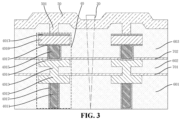
- FIG. 2 is a sectional view between the adjacent sealing structures 20 .
- the sealing structure 20 includes a metal wall body 40 and a blocking wall body 501 located on a top of the metal wall body 40 .
- the metal wall body 40 and the blocking wall body 501 both are disposed around the chip structure 10 .
- the semiconductor structure further includes an interlayer dielectric layer and an etching stop layer.
- the metal wall body 40 and the blocking wall body 501 are located in the interlayer dielectric layer and the etching stop layer.
- the interlayer dielectric layer, the etching stop layer and the metal wall body 40 can prevent external air, water vapor and the like from being in contact with the chip structure 10 , so as to realize the protection on the chip structure 10 .
- the interlayer dielectric layer and the etching stop layer can be made of an insulation material.
- a material of the interlayer dielectric layer may be silicon oxide.
- the material of the interlayer dielectric layer in the present embodiment may also be silicon oxynitride, silicon nitride and the like.
- a material of the metal wall body 40 may include copper, tungsten, aluminum and the like.
- the metal wall body 40 is not limited in the present embodiment.
- a material of the etching stop layer may be silicon oxynitride, silicon carbonitride and the like. It should be noted that the materials of the interlayer dielectric layer and the etching stop layer are different.
- the metal wall body 40 may include a plurality of sub wall bodies sequentially stacked in a direction perpendicular to the substrate, and projections of adjacent sub wall bodies on the substrate at least partially overlap. It is worth noting that each of the sub wall bodies is made of a metal material. The material of each of the sub wall bodies may be identical and may also be different, which is not limited in the present embodiment. Through such an arrangement, the metal wall body 40 is formed by stacking a plurality of sub wall bodies, and the manufacturing difficulty of the metal wall body 40 can be reduced. Additionally, the projections of adjacent sub wall bodies on the substrate at least partially overlap, so that the adjacent sub wall bodies are at least partially connected, improving the sealing effect.
- the interlayer dielectric layer includes a plurality of sub interlayer dielectric layers sequentially stacked in a direction perpendicular to the substrate.
- Each of the sub interlayer dielectric layers is at least disposed in the same layer as a sub wall body.
- a sub interlayer dielectric layer may be firstly formed, and then, a notch is formed on the sub interlayer dielectric layer, and the sub wall body is formed in the notch.
- a sealing structure 20 is formed by repeating the above operation.
- a metal layer may be firstly formed, a part of the metal layer is removed to form the sub wall body, and then, the sub interlayer dielectric layer disposed in the same layer as the sub wall body is formed.
- the sealing structure 20 may also be formed by repeating the above operation. Further, an etching stop layer is further disposed between the sub interlayer dielectric layers.
- each of the sub wall bodies is disposed in the same layer as a metal layer in the chip structure 10 .
- the metal layer in the chip structure 10 and the sub wall body may be formed at the same time, which simplifies manufacturing operations of the semiconductor structure, and further reduces the manufacturing difficulty of the semiconductor structure.
- each of the sub wall bodies is disposed in the same layer as a metal layer in the chip structure 10
- the material of the sub interlayer dielectric layers forming the interlayer dielectric layer may be identical, partially identical or completely different
- the material of the sub wall bodies forming the metal wall body 40 may be identical, partially identical or completely different.
- the metal wall body 40 may include 6 sub wall bodies sequentially stacked in a direction away from the substrate (not shown in the figure), the 6 sub wall bodies are respectively a first sub wall body 4011 , a second sub wall body 4012 , a third sub wall body 4013 , a fourth sub wall body 4014 , a fifth sub wall body 4015 and a sixth sub wall body 4016 .
- the first sub wall body 4011 and the fifth sub wall body 4015 may be made of tungsten
- the second sub wall body 4012 , the third sub wall body 4013 and the fourth sub wall body 4014 may be made of copper
- the sixth sub wall body 4016 may be made of aluminum.
- a blocking layer 4017 is disposed on side surfaces, perpendicular to the substrate, of the first sub wall body 4011 and the fifth sub wall body 4015 and the side surfaces, close to the substrate, of the first sub wall body 4011 and the fifth sub wall body 4015 .
- the blocking layer 4017 is also disposed on two side surfaces, parallel to the substrate, of the sixth sub wall body 4016 .
- a material of the blocking layer 4017 may include titanium or titanium nitride.
- the interlayer dielectric layer may include a first sub interlayer dielectric layer 601 , a second sub interlayer dielectric layer 602 and a third sub interlayer dielectric layer 603 .
- the etching stop layer may include a first sub etching stop layer 701 and a second sub etching stop layer 702 .
- the first sub etching stop layer 701 is located between the first sub interlayer dielectric layer 601 and the second sub interlayer dielectric layer 602 .
- the second sub etching stop layer 702 is located between the second sub interlayer dielectric layer 602 and the third sub interlayer dielectric layer 603 .
- the metal wall body 40 is disposed in the interlayer dielectric layer. That is to say, when the interlayer dielectric layer covers the side walls, perpendicular to the substrate, of the metal wall body 40 , at least a part of the interlayer dielectric layer also covers a top of the metal wall body 40 away from the substrate.
- the blocking wall body 501 is disposed on the top of the metal wall body 40 . Specifically, the blocking wall body 501 is located on a side, away from the substrate, of the metal wall body 40 , and additionally, the blocking wall body 501 is disposed directly facing the top of the metal wall. As shown in FIG. 2 and FIG. 3 , when a cutting seam 30 is formed on a cutting channel 21 during cutting a wafer, the blocking wall body 501 can prevent the cracks in the interlayer dielectric layer of a side, away from the substrate, of the metal wall body 40 from extending to the chip structure 10 , thereby avoiding the failures of the chip structure 10 .
- a bottom end, away from the substrate, of the blocking wall body 501 is in contact with the top end of at least a part of the metal wall body 40 , so as to prevent a gap from generating between the blocking wall body 501 and the metal wall body 40 and prevent the cracks from extending to the chip structure 10 along the gap.
- the blocking wall body 501 may be located in the interlayer dielectric layer. That is to say, a thickness of the blocking wall body in a direction perpendicular to the substrate is smaller than a thickness of the interlayer dielectric layer on the top end of the metal wall body 40 .
- the thickness of the blocking wall body 501 in a direction perpendicular to the substrate equals to the thickness of the interlayer dielectric layer on the top end of the metal wall body 40 .
- a blocking trench may be formed on a side surface, away from the substrate, of the interlayer dielectric layer, the blocking trench extends to the top end of the blocking wall body 501 , additionally, a trench bottom of the blocking trench is in contact with the top end of the metal wall body 40 , and the blocking trench is filled with the blocking wall body 501 .
- the cracks may be further prevented from extending to the chip structure 10 along the interlayer dielectric layer on a side, away from the substrate, of the metal wall body 40 when a cutting seam 30 is formed.
- the blocking wall body 501 is disposed on the top end of the metal wall body 40 .
- the blocking wall body 501 covers at least a part of a top surface of the metal wall body 40 , so as to further prevent the cracks from extending to the chip structure 10 along a path between the blocking wall body 501 and the metal wall body 40 and to further improve the sealing effect on the chip structure 10 .
- the sixth sub wall body 4016 of the metal wall body 40 is located on the top end of the metal wall body 40 , a projection of the blocking wall body 501 on the substrate is located inside the projection of the sixth sub wall body 4016 on the substrate, so that the blocking wall body 501 covers a part of the sixth sub wall body 4016 .
- a plurality of chip structures 10 may be manufactured on the substrate (such as a silicon wafer), and a sealing structure 20 is formed on the periphery of each of the semiconductor structures. Then, the silicon wafer is cut, so as to form cutting seams 30 between the adjacent sealing structures 20 to obtain a plurality of separate chips.
- a chip structure 10 and a the sealing structure 20 are disposed on the substrate, the sealing structure 20 includes a metal wall body 40 and a blocking wall body 501 located on the top of the metal wall body 40 , and the metal wall body 40 and the blocking wall body 501 both are disposed around the chip structure 10 .
- the blocking wall body 501 can prevent the cracks from extending to the chip structure 10 along the interlayer dielectric layer at one side, away from the substrate, of the metal wall body 40 , and thereby avoiding the failure of the chip structure 10 .
- the number of blocking wall body 501 may be multiple, and the multiple blocking wall bodies 501 are disposed at intervals around the chip structure 10 . Additionally, the multiple blocking wall bodies 501 are all located on a top of the metal wall body 40 . Through such an arrangement, the multiple blocking wall bodies 501 may provide multiplex protection to further improve the protection effect.
- the multiple blocking wall bodies 501 are all located on the top of the same metal wall body 40 .
- the multiple blocking wall bodies 501 are disposed on the top of the same sixth sub wall body 4016 at intervals, which reduces an area occupied by the sealing structures and improves the protection effect at the same time.
- the semiconductor structure provided by the present embodiment further includes a sealing layer 50 disposed on a side of the sealing structure 20 away from the substrate.
- the sealing layer 50 covers the sealing structure 20 , which further improves the protection effect and sealing effect on the chip structure 10 .
- the sealing layer 50 may be located on a side, away from the substrate, of the interlayer dielectric layer.
- the sealing layer 50 may be integral with the blocking wall body 501 .
- the blocking wall body 501 and the sealing layer 50 may be formed through the same manufacturing operation, and the manufacturing difficulty of the semiconductor structure is simplified.
- a top surface of a part of the sealing layer 50 on the blocking wall body 501 is higher than a top surface of a part of the sealing layer 50 on the cutting channel 21 .
- the sealing layer 50 on a structure between the blocking wall body 501 and the cutting channel 21 has a slope.
- a material of the blocking wall body 501 includes an insulation material.
- the material of the blocking wall body 501 may include silicon nitride, silicon oxynitride and the like.
- the material of the sealing layer 50 is the same as the material of the blocking wall body 501 .
- An embodiment of the present disclosure further provides a manufacturing method of a semiconductor structure.
- the manufacturing method is used for manufacturing the semiconductor structure in the embodiment above.
- a chip structure and a sealing structure are disposed on the substrate of the semiconductor structure.
- the sealing structure includes a metal wall body and a blocking wall body located on the top of the metal wall body.
- the metal wall body and the blocking wall body both are disposed around the chip structure.
- the blocking wall body can prevent the cracks from extending to the chip structure within the interlayer dielectric layer on a side, away from the substrate, of the metal wall body, and thereby avoiding the failure of the chip structure.
- the embodiment of the present disclosure further provides a manufacturing method of the semiconductor structure, which includes the following operations.
- the substrate may include a wafer made of semiconductor materials, such as a silicon wafer, a germanium wafer, a gallium nitride wafer, a gallium germanide wafer, a gallium arsenide wafer and an SOI wafer.
- a wafer made of semiconductor materials such as a silicon wafer, a germanium wafer, a gallium nitride wafer, a gallium germanide wafer, a gallium arsenide wafer and an SOI wafer.
- a plurality of chip structures may be disposed at intervals on the silicon wafer.
- the sealing structure is disposed on the periphery of each of the chip structures.
- the structure between the sealing structures on the periphery of the adjacent chip structures is a cutting channel.
- the blocking wall body is disposed on the top of the metal wall body, and the blocking wall body can prevent the cracks from extending to the chip structures along a side, away from the substrate, of the metal wall body during cutting the wafer, i.e., during the formation of a cutting seam in the cutting channel, and thereby avoiding the failure of the chip structures.
- Chip structures 10 corresponding to different types of chips may be different.
- a chip structure 10 of a logic chip may include a device structure at a front section and a metal interconnection structure at a rear section.
- a chip structure 10 of a dynamic random access memory chip may include a device structure at a front section, a capacitance structure at a middle section and a metal interconnection structure at a rear section.
- the device structure includes a planar transistor, an embedded gate transistor, a fin transistor, a surrounding gate transistor and the like.
- the operation of forming the chip structure and the sealing structure on the substrate includes the following details.
- a plurality of sub interlayer dielectric layers, a plurality of sub wall bodies and a top-layer metal layer 402 are formed on the substrate (not shown in the figure). Specifically, a first sub interlayer dielectric layer 601 , a second sub interlayer dielectric layer 602 and a top-layer dielectric layer 6031 are sequentially formed on the substrate. The first sub wall body 4011 and the second sub wall body 4012 are located in the first sub interlayer dielectric layer 601 .
- the third sub wall body 4013 and the fourth sub wall body 4014 are located in the second sub interlayer dielectric layer 602 , the fifth sub wall body 4015 is located in the top-layer dielectric layer 6031 , the top-layer metal layer 402 is located on the top-layer dielectric layer 6031 , and the top-layer metal layer 402 is connected with the sub wall body, and specifically, the top-layer metal layer 402 is connected with the fifth sub wall body 4015 .
- the chip structure (not shown in the figure) can be formed at the same time.
- the sub wall body is located on the outer side of the chip structure, and is disposed around the chip structure. Specifically, the chip structure and the sub wall body may be formed at the same time in the same process operations such as deposition, photo-etching and etching.
- the method further includes forming an etching stop layer.
- the etching stop layer may include a first sub etching stop layer 701 and a second sub etching stop layer 702 .
- the first sub etching stop layer 701 is located between the first sub interlayer dielectric layer 601 and the second sub interlayer dielectric layer 602
- the second sub etching stop layer 702 is located between the second sub interlayer dielectric layer 602 and the top-layer dielectric layer 6031 .
- the method further includes removing a part of the top-layer metal layer 402 to form a metal block 403 connected with both the sub wall body and the top-layer dielectric layer.
- a part of the top-layer metal layer 402 may be removed in modes of photo-etching, etching and the like.
- the metal block 403 may also be used as a sub wall body and is disposed around the chip structure.
- the method further includes forming a covering layer on the metal block 403 .
- a material of the covering layer may be identical to the material of the top-layer dielectric layer, so as to achieve a better combination effect. Therefore, during cutting a wafer, peeling does not easily occur.
- the material of the covering layer and the top-layer dielectric layer is silicon oxide.
- the covering layer and the top-layer dielectric layer jointly form the third sub interlayer dielectric layer 603 , and the third sub interlayer dielectric layer 603 covers the metal block 403 .
- a photoresist layer 70 with an opening 71 is formed on the covering layer, and the opening 71 is located on the sub wall bodies.
- the covering layer is etched by taking the photoresist layer as a mask so as to form a blocking trench 603 exposing the metal block 403 .
- the blocking trench 603 is filled with a blocking material to form the blocking wall body 501 .
- the metal block 403 may be used as a sub wall body.
- the metal block 403 and other sub wall bodies together form a metal wall body 40 .
- a blocking trench 603 is formed in an etching manner, and then, the blocking wall body 501 is formed in the blocking trench 603 , which improves the position and dimension precision of the blocking wall body 501 . Additionally, the blocking trench 603 extends to a corresponding metal block 403 from a top surface, away from the substrate, of the covering layer to further expose the corresponding metal block 403 .
- the blocking wall body 501 is formed, the blocking wall body 501 is in contact with the metal block 403 , and the cracks can be prevented from extending to the chip structure along a path between the blocking wall body 501 and the metal wall body 40 .
- a material of the sub wall body and the metal block 403 may include copper, tungsten, aluminum and the like.
- the metal wall body 40 is not limited in the present embodiment.
- the number of the sub wall body may be multiple, the multiple sub wall bodies are stacked, each of the sub wall bodies is disposed in the same layer as a metal layer in the chip structure, and the manufacturing difficulty of the semiconductor structure can be simplified. It is worth noting that the projections of adjacent sub wall bodies on the substrate at least partially overlap so as to avoid the formation of a gap between the adjacent sub wall bodies.
- the plurality of sub wall bodies may include a first sub wall body 4011 , a second sub wall body 4012 , a third sub wall body 4013 , a fourth sub wall body 4014 and a fifth sub wall body 4015 sequentially disposed in a direction away from the substrate (not shown in the figure).
- the first sub wall body 4011 and the fifth sub wall body 4015 may be made of tungsten
- the second sub wall body 4012 , the third sub wall body 4013 and the fourth sub wall body 4014 may be made of copper
- the metal block 403 may be made of aluminum.
- a blocking layer 4017 is disposed on the side surfaces, perpendicular to the substrate, of the first sub wall body 4011 and the fifth sub wall body 4015 , and the side surfaces close to the substrate, of the first sub wall body 4011 and the fifth sub wall body 4015 .
- the blocking layer 4017 is also disposed on two side surfaces, parallel to the substrate, of the metal block 403 .
- a material of the blocking layer 4017 may include titanium or titanium nitride.
- the operation of manufacturing the blocking wall body 501 of the manufacturing method of a semiconductor structure provided by the present embodiment includes forming a sealing material on the covering layer, filling the blocking trench 603 with a part of the sealing material so as to form the blocking wall body 501 , and covering the covering layer with a part of the sealing material to form the sealing layer 50 .
- the sealing layer 50 is integral with the blocking wall body 501 .
- the sealing layer 50 is integral with the blocking wall body 501 .
- the sealing layer 50 may be a silicon nitride layer.
- the blocking wall body 501 may also be made of silicon nitride.
- a top surface of a part of the sealing layer 50 on the blocking wall body 501 is higher than a top surface of a part of the sealing layer 50 on the cutting channel 21 .
- the sealing layer 50 on a structure between the blocking wall body 501 and the cutting channel 21 has a slope.
- a chip structure and a sealing structure are disposed on the substrate, the sealing structure includes a metal wall body 40 and a blocking wall body 501 located on the top of the metal wall body 40 , and the metal wall body 40 and the blocking wall body 501 both are disposed around the chip structure 10 .
- the blocking wall body 501 can prevent the cracks from extending to the chip structure along the interlayer dielectric layer on a side, away from the substrate, of the metal wall body 40 , and therefore avoiding the failure of the chip structure.
Landscapes
- Dicing (AREA)
- Internal Circuitry In Semiconductor Integrated Circuit Devices (AREA)
Abstract
Description
Claims (10)
Applications Claiming Priority (3)
| Application Number | Priority Date | Filing Date | Title |
|---|---|---|---|
| CN202110224400.0 | 2021-03-01 | ||
| CN202110224400.0A CN113035835B (en) | 2021-03-01 | 2021-03-01 | Semiconductor structure and semiconductor structure fabrication method |
| PCT/CN2021/104791 WO2022183647A1 (en) | 2021-03-01 | 2021-07-06 | Semiconductor structure and semiconductor structure manufacturing method |
Related Parent Applications (1)
| Application Number | Title | Priority Date | Filing Date |
|---|---|---|---|
| PCT/CN2021/104791 Continuation WO2022183647A1 (en) | 2021-03-01 | 2021-07-06 | Semiconductor structure and semiconductor structure manufacturing method |
Publications (2)
| Publication Number | Publication Date |
|---|---|
| US20220278054A1 US20220278054A1 (en) | 2022-09-01 |
| US12191263B2 true US12191263B2 (en) | 2025-01-07 |
Family
ID=83006708
Family Applications (1)
| Application Number | Title | Priority Date | Filing Date |
|---|---|---|---|
| US17/648,130 Active 2042-06-22 US12191263B2 (en) | 2021-03-01 | 2022-01-16 | Semiconductor structure and manufacturing method of semiconductor structure |
Country Status (1)
| Country | Link |
|---|---|
| US (1) | US12191263B2 (en) |
Citations (9)
| Publication number | Priority date | Publication date | Assignee | Title |
|---|---|---|---|---|
| US20060012012A1 (en) | 2004-07-15 | 2006-01-19 | Ping-Wei Wang | Semiconductor device with crack prevention ring and method of manufacture thereof |
| US7400028B2 (en) | 2004-06-21 | 2008-07-15 | Renesas Technology Corp. | Semiconductor device |
| US20100078769A1 (en) | 2008-09-23 | 2010-04-01 | Texas Instruments Incorporated | Environmental die seal enhancement for wafer level chip scale packages |
| US20120104541A1 (en) | 2010-11-03 | 2012-05-03 | Taiwan Semiconductor Manufacturing Company, Ltd. | Seal ring structure with polyimide layer adhesion |
| US20120313217A1 (en) * | 2011-06-13 | 2012-12-13 | Mediatek Inc. | Seal ring structure with capacitor |
| US20140035128A1 (en) | 2012-07-31 | 2014-02-06 | Taiwan Semiconductor Manufacturing Company Limited | Semiconductor seal ring |
| US20170186732A1 (en) * | 2015-12-29 | 2017-06-29 | Taiwan Semiconductor Manufacturing Co., Ltd. | Seal-ring structure for stacking integrated circuits |
| CN113035835A (en) | 2021-03-01 | 2021-06-25 | 长鑫存储技术有限公司 | Semiconductor structure and manufacturing method thereof |
| US20210210440A1 (en) * | 2020-01-08 | 2021-07-08 | Texas Instruments Incorporated | Integrated circuit with metal stop ring outside the scribe seal |
-
2022
- 2022-01-16 US US17/648,130 patent/US12191263B2/en active Active
Patent Citations (15)
| Publication number | Priority date | Publication date | Assignee | Title |
|---|---|---|---|---|
| US7400028B2 (en) | 2004-06-21 | 2008-07-15 | Renesas Technology Corp. | Semiconductor device |
| US20060012012A1 (en) | 2004-07-15 | 2006-01-19 | Ping-Wei Wang | Semiconductor device with crack prevention ring and method of manufacture thereof |
| CN1734764A (en) | 2004-07-15 | 2006-02-15 | 台湾积体电路制造股份有限公司 | Semiconductor device with crack-preventing ring structure and manufacturing method thereof |
| US7223673B2 (en) | 2004-07-15 | 2007-05-29 | Taiwan Semiconductor Manufacturing Company, Ltd. | Method of manufacturing semiconductor device with crack prevention ring |
| US20100078769A1 (en) | 2008-09-23 | 2010-04-01 | Texas Instruments Incorporated | Environmental die seal enhancement for wafer level chip scale packages |
| US8125054B2 (en) | 2008-09-23 | 2012-02-28 | Texas Instruments Incorporated | Semiconductor device having enhanced scribe and method for fabrication |
| US20120104541A1 (en) | 2010-11-03 | 2012-05-03 | Taiwan Semiconductor Manufacturing Company, Ltd. | Seal ring structure with polyimide layer adhesion |
| CN102468247A (en) | 2010-11-03 | 2012-05-23 | 台湾积体电路制造股份有限公司 | Seal ring structure with polyimide layer adhesion |
| US8587089B2 (en) | 2010-11-03 | 2013-11-19 | Taiwan Semiconductor Manufacturing Company, Ltd. | Seal ring structure with polyimide layer adhesion |
| US20120313217A1 (en) * | 2011-06-13 | 2012-12-13 | Mediatek Inc. | Seal ring structure with capacitor |
| US20140035128A1 (en) | 2012-07-31 | 2014-02-06 | Taiwan Semiconductor Manufacturing Company Limited | Semiconductor seal ring |
| US8987923B2 (en) | 2012-07-31 | 2015-03-24 | Taiwan Semiconductor Manufacturing Company Limited | Semiconductor seal ring |
| US20170186732A1 (en) * | 2015-12-29 | 2017-06-29 | Taiwan Semiconductor Manufacturing Co., Ltd. | Seal-ring structure for stacking integrated circuits |
| US20210210440A1 (en) * | 2020-01-08 | 2021-07-08 | Texas Instruments Incorporated | Integrated circuit with metal stop ring outside the scribe seal |
| CN113035835A (en) | 2021-03-01 | 2021-06-25 | 长鑫存储技术有限公司 | Semiconductor structure and manufacturing method thereof |
Also Published As
| Publication number | Publication date |
|---|---|
| US20220278054A1 (en) | 2022-09-01 |
Similar Documents
| Publication | Publication Date | Title |
|---|---|---|
| US12243777B2 (en) | Semiconductor device and method of manufacturing the same | |
| US8022455B2 (en) | Method of fabricating semiconductor device for reducing parasitic capacitance between bit lines and semiconductor device fabricated thereby | |
| US10325802B2 (en) | Method for fabricating semiconductor device | |
| US11664435B2 (en) | Dynamic random access memory and method of fabricating the same | |
| CN113035835B (en) | Semiconductor structure and semiconductor structure fabrication method | |
| US20240284664A1 (en) | Semiconductor device | |
| TWI765694B (en) | Semiconductor memory structure and method for forming the same | |
| US12191263B2 (en) | Semiconductor structure and manufacturing method of semiconductor structure | |
| US12512429B2 (en) | Semiconductor device and method of manufacturing the same | |
| US20240098987A1 (en) | Semiconductor device and manufacturing method thereof | |
| US12324148B2 (en) | Method for forming semiconductor structure and a semiconductor | |
| US20230247825A1 (en) | Semiconductor device | |
| US6853050B2 (en) | Semiconductor device with fuse box and method for fabricating the same | |
| US20250006801A1 (en) | Method for fabricating semiconductor device | |
| US12457788B2 (en) | Semiconductor device and method for manufacturing the same | |
| CN112018117A (en) | Semiconductor device with a plurality of transistors | |
| US20240324181A1 (en) | Semiconductor device and manufacturing method thereof | |
| EP4311387A1 (en) | Semiconductor device | |
| CN118742032B (en) | A method for preparing a semiconductor structure and a semiconductor structure thereof | |
| US20230369141A1 (en) | Semiconductor device and method of manufacturing the same | |
| US20250024660A1 (en) | Semiconductor device and method for fabricating the same | |
| US20250096162A1 (en) | Semiconductor structure and manufacturing method therefor | |
| US20240381624A1 (en) | Semiconductor devices and manufacturing methods thereof | |
| US20250273569A1 (en) | Semiconductor device | |
| US20260052668A1 (en) | Semiconductor device and method of manufacturing the same |
Legal Events
| Date | Code | Title | Description |
|---|---|---|---|
| AS | Assignment |
Owner name: CHANGXIN MEMORY TECHNOLOGIES, INC., CHINA Free format text: ASSIGNMENT OF ASSIGNORS INTEREST;ASSIGNORS:WANG, MENGMENG;HUANG, HSIN-PIN;REEL/FRAME:058667/0415 Effective date: 20210708 |
|
| FEPP | Fee payment procedure |
Free format text: ENTITY STATUS SET TO UNDISCOUNTED (ORIGINAL EVENT CODE: BIG.); ENTITY STATUS OF PATENT OWNER: LARGE ENTITY |
|
| STPP | Information on status: patent application and granting procedure in general |
Free format text: DOCKETED NEW CASE - READY FOR EXAMINATION |
|
| STPP | Information on status: patent application and granting procedure in general |
Free format text: NON FINAL ACTION MAILED |
|
| STPP | Information on status: patent application and granting procedure in general |
Free format text: RESPONSE TO NON-FINAL OFFICE ACTION ENTERED AND FORWARDED TO EXAMINER |
|
| STPP | Information on status: patent application and granting procedure in general |
Free format text: NON FINAL ACTION MAILED |
|
| STPP | Information on status: patent application and granting procedure in general |
Free format text: NOTICE OF ALLOWANCE MAILED -- APPLICATION RECEIVED IN OFFICE OF PUBLICATIONS |
|
| STPP | Information on status: patent application and granting procedure in general |
Free format text: PUBLICATIONS -- ISSUE FEE PAYMENT RECEIVED |
|
| STPP | Information on status: patent application and granting procedure in general |
Free format text: PUBLICATIONS -- ISSUE FEE PAYMENT VERIFIED |
|
| STCF | Information on status: patent grant |
Free format text: PATENTED CASE |