US12189532B2 - Fault tolerance and coherence for shared memory - Google Patents
Fault tolerance and coherence for shared memory Download PDFInfo
- Publication number
- US12189532B2 US12189532B2 US17/853,752 US202217853752A US12189532B2 US 12189532 B2 US12189532 B2 US 12189532B2 US 202217853752 A US202217853752 A US 202217853752A US 12189532 B2 US12189532 B2 US 12189532B2
- Authority
- US
- United States
- Prior art keywords
- nodes
- memory
- cache
- data
- blast
- Prior art date
- Legal status (The legal status is an assumption and is not a legal conclusion. Google has not performed a legal analysis and makes no representation as to the accuracy of the status listed.)
- Active
Links
Images


Classifications
-
- G—PHYSICS
- G06—COMPUTING OR CALCULATING; COUNTING
- G06F—ELECTRIC DIGITAL DATA PROCESSING
- G06F12/00—Accessing, addressing or allocating within memory systems or architectures
- G06F12/02—Addressing or allocation; Relocation
- G06F12/08—Addressing or allocation; Relocation in hierarchically structured memory systems, e.g. virtual memory systems
- G06F12/0802—Addressing of a memory level in which the access to the desired data or data block requires associative addressing means, e.g. caches
- G06F12/0806—Multiuser, multiprocessor or multiprocessing cache systems
- G06F12/0815—Cache consistency protocols
- G06F12/0817—Cache consistency protocols using directory methods
- G06F12/0824—Distributed directories, e.g. linked lists of caches
-
- G—PHYSICS
- G06—COMPUTING OR CALCULATING; COUNTING
- G06F—ELECTRIC DIGITAL DATA PROCESSING
- G06F12/00—Accessing, addressing or allocating within memory systems or architectures
- G06F12/02—Addressing or allocation; Relocation
- G06F12/08—Addressing or allocation; Relocation in hierarchically structured memory systems, e.g. virtual memory systems
- G06F12/0802—Addressing of a memory level in which the access to the desired data or data block requires associative addressing means, e.g. caches
- G06F12/0806—Multiuser, multiprocessor or multiprocessing cache systems
- G06F12/0813—Multiuser, multiprocessor or multiprocessing cache systems with a network or matrix configuration
-
- G—PHYSICS
- G06—COMPUTING OR CALCULATING; COUNTING
- G06F—ELECTRIC DIGITAL DATA PROCESSING
- G06F11/00—Error detection; Error correction; Monitoring
- G06F11/07—Responding to the occurrence of a fault, e.g. fault tolerance
- G06F11/08—Error detection or correction by redundancy in data representation, e.g. by using checking codes
- G06F11/10—Adding special bits or symbols to the coded information, e.g. parity check, casting out 9's or 11's
-
- G—PHYSICS
- G06—COMPUTING OR CALCULATING; COUNTING
- G06F—ELECTRIC DIGITAL DATA PROCESSING
- G06F11/00—Error detection; Error correction; Monitoring
- G06F11/07—Responding to the occurrence of a fault, e.g. fault tolerance
- G06F11/14—Error detection or correction of the data by redundancy in operation
-
- G—PHYSICS
- G06—COMPUTING OR CALCULATING; COUNTING
- G06F—ELECTRIC DIGITAL DATA PROCESSING
- G06F11/00—Error detection; Error correction; Monitoring
- G06F11/30—Monitoring
- G06F11/3003—Monitoring arrangements specially adapted to the computing system or computing system component being monitored
- G06F11/3037—Monitoring arrangements specially adapted to the computing system or computing system component being monitored where the computing system component is a memory, e.g. virtual memory, cache
-
- G—PHYSICS
- G06—COMPUTING OR CALCULATING; COUNTING
- G06F—ELECTRIC DIGITAL DATA PROCESSING
- G06F12/00—Accessing, addressing or allocating within memory systems or architectures
- G06F12/02—Addressing or allocation; Relocation
- G06F12/0223—User address space allocation, e.g. contiguous or non contiguous base addressing
- G06F12/0284—Multiple user address space allocation, e.g. using different base addresses
-
- G—PHYSICS
- G06—COMPUTING OR CALCULATING; COUNTING
- G06F—ELECTRIC DIGITAL DATA PROCESSING
- G06F12/00—Accessing, addressing or allocating within memory systems or architectures
- G06F12/02—Addressing or allocation; Relocation
- G06F12/08—Addressing or allocation; Relocation in hierarchically structured memory systems, e.g. virtual memory systems
- G06F12/0802—Addressing of a memory level in which the access to the desired data or data block requires associative addressing means, e.g. caches
- G06F12/0806—Multiuser, multiprocessor or multiprocessing cache systems
- G06F12/0815—Cache consistency protocols
- G06F12/0837—Cache consistency protocols with software control, e.g. non-cacheable data
-
- G—PHYSICS
- G06—COMPUTING OR CALCULATING; COUNTING
- G06F—ELECTRIC DIGITAL DATA PROCESSING
- G06F12/00—Accessing, addressing or allocating within memory systems or architectures
- G06F12/02—Addressing or allocation; Relocation
- G06F12/08—Addressing or allocation; Relocation in hierarchically structured memory systems, e.g. virtual memory systems
- G06F12/0802—Addressing of a memory level in which the access to the desired data or data block requires associative addressing means, e.g. caches
- G06F12/0806—Multiuser, multiprocessor or multiprocessing cache systems
- G06F12/084—Multiuser, multiprocessor or multiprocessing cache systems with a shared cache
-
- G—PHYSICS
- G06—COMPUTING OR CALCULATING; COUNTING
- G06F—ELECTRIC DIGITAL DATA PROCESSING
- G06F15/00—Digital computers in general; Data processing equipment in general
- G06F15/16—Combinations of two or more digital computers each having at least an arithmetic unit, a program unit and a register, e.g. for a simultaneous processing of several programs
- G06F15/163—Interprocessor communication
- G06F15/167—Interprocessor communication using a common memory, e.g. mailbox
-
- G—PHYSICS
- G06—COMPUTING OR CALCULATING; COUNTING
- G06F—ELECTRIC DIGITAL DATA PROCESSING
- G06F12/00—Accessing, addressing or allocating within memory systems or architectures
- G06F12/02—Addressing or allocation; Relocation
- G06F12/0223—User address space allocation, e.g. contiguous or non contiguous base addressing
- G06F12/0292—User address space allocation, e.g. contiguous or non contiguous base addressing using tables or multilevel address translation means
-
- G—PHYSICS
- G06—COMPUTING OR CALCULATING; COUNTING
- G06F—ELECTRIC DIGITAL DATA PROCESSING
- G06F12/00—Accessing, addressing or allocating within memory systems or architectures
- G06F12/02—Addressing or allocation; Relocation
- G06F12/08—Addressing or allocation; Relocation in hierarchically structured memory systems, e.g. virtual memory systems
- G06F12/10—Address translation
-
- G—PHYSICS
- G06—COMPUTING OR CALCULATING; COUNTING
- G06F—ELECTRIC DIGITAL DATA PROCESSING
- G06F2212/00—Indexing scheme relating to accessing, addressing or allocation within memory systems or architectures
- G06F2212/10—Providing a specific technical effect
- G06F2212/1032—Reliability improvement, data loss prevention, degraded operation etc
-
- G—PHYSICS
- G06—COMPUTING OR CALCULATING; COUNTING
- G06F—ELECTRIC DIGITAL DATA PROCESSING
- G06F2212/00—Indexing scheme relating to accessing, addressing or allocation within memory systems or architectures
- G06F2212/10—Providing a specific technical effect
- G06F2212/1048—Scalability
-
- G—PHYSICS
- G06—COMPUTING OR CALCULATING; COUNTING
- G06F—ELECTRIC DIGITAL DATA PROCESSING
- G06F2212/00—Indexing scheme relating to accessing, addressing or allocation within memory systems or architectures
- G06F2212/15—Use in a specific computing environment
- G06F2212/154—Networked environment
-
- G—PHYSICS
- G06—COMPUTING OR CALCULATING; COUNTING
- G06F—ELECTRIC DIGITAL DATA PROCESSING
- G06F2212/00—Indexing scheme relating to accessing, addressing or allocation within memory systems or architectures
- G06F2212/25—Using a specific main memory architecture
- G06F2212/254—Distributed memory
Definitions
- a shared memory can be accessed by multiple cores or processors via an interconnect between the shared memory and the processors.
- the shared memory can be distributed across multiple memory devices that are accessed via an interconnect or network by processing devices.
- the shared memory can serve as a main memory that can enable faster access to cache lines or data blocks that are expected to be more frequently accessed by the processors, cores, or processing devices, as compared to accessing the data from storage devices, such as Hard Disk Drives (HDDs), tape drives, or certain types of Solid-State Drives (SSDs).
- HDDs Hard Disk Drives
- SSDs Solid-State Drives
- a memory coherence protocol can be used to ensure that copies of the same data are coherent or consistent throughout the system.
- Memory coherence protocols typically assume accurate communication between the devices in the system and rely on redundant copies of the data stored in the memory to also be stored in storage devices for handling physical failures of system components, such as bad connectors or worn out memory devices.
- systems may use replay buffers or error correcting codes to correct or resend messages that may have errors due to errors in the interconnect or the network that may be caused by noise.
- supercomputers or data centers may provide checkpointing by periodically copying an entire memory to a storage device, such as an HDD.
- a storage device such as an HDD.
- operation of the supercomputer may be halted while data from the failed memory regions are recovered from the checkpointed data in the storage device.
- Such halting of operations becomes more frequent as the size of the supercomputer or data center increases such that the performance of the overall system suffers.
- maintaining the coherency of data throughout large-scale systems becomes more difficult as the size of the system increases since there can be more copies of a greater number of cache lines being accessed by a greater number of processing devices.
- FIG. 1 is a block diagram of an example system including a shared memory for implementing memory fault tolerance and memory coherence according to one or more embodiments.
- FIG. 2 is a block diagram of an example distributed system for implementing memory fault tolerance and memory coherence according to one or more embodiments.
- FIG. 3 provides an example arrangement of memory according to one or more embodiments.
- FIG. 4 is a sequence diagram for a read/write sequence according to one or more embodiments.
- FIG. 5 is a sequence diagram for a contention resolution sequence according to one or more embodiments.
- FIG. 6 A is a first part of a sequence diagram for a rebuild sequence according to one or more embodiments.
- FIG. 6 B is a second part of the sequence diagram for the rebuild sequence from FIG. 6 A according to one or more embodiments.
- FIG. 7 is a flowchart for a memory configuration process according to one or more embodiments.
- FIG. 8 is a flowchart for a rebuild process according to one or more embodiments.
- FIG. 1 is a block diagram of an example system for implementing memory coherence and memory fault tolerance according to one or more embodiments.
- System 100 in FIG. 1 may function as, for example, a multi-core computer, a System on a Chip (SoC), or a supercomputer that processes data stored in shared memory 112 .
- SoC System on a Chip
- system 100 includes processors 102 , caches 104 , interconnect 110 , and shared memory 112 .
- Each of processors 102 1 to 102 N can include, for example, circuitry such as one or more RISC-V cores or other type of Central Processing Unit (CPU), a Graphics Processing Unit (GPU), a microcontroller, a Digital Signal Processor (DSP), an Application-Specific Integrated Circuit (ASIC), a Field Programmable Gate Array (FPGA), hard-wired logic, analog circuitry and/or a combination thereof.
- each processor 102 may comprise a multi-core processor or each processor 102 can represent a single processing core.
- a processor 102 can include an SoC or other type of integrated processing system that includes a cache 104 to form a processing unit 101 .
- each processor 102 can include one or more levels of cache memory not shown in FIG. 1 , such as L1, L2, and/or L3 caches.
- Processors 102 1 to 102 N use respective caches 104 1 to 104 N as a Last Level Cache (LLC) (e.g., an L2, L3, or L4 cache depending on the levels of cache included in the processor 102 ) that caches data blocks or cache lines that are requested by the processor 102 or expected to be accessed by the processor 102 .
- LLC Last Level Cache
- Cache controllers 106 control the operation of their respective cache memories 108 to retrieve cache lines from shared memory 112 via interconnect 110 and store the retrieved cache lines in cache memory 108 for access by processor 102 .
- cache controllers 106 can retrieve cache lines from shared memory 112 based on commands received from its respective processor 102 , and in some implementations, may also retrieve or prefetch additional cache lines that are expected to be used by processor 102 .
- Interconnect 110 can include, for example, a Peripheral Component Interconnect express (PCIe) bus, a Network on a Chip (NoC), or another type of bus or network.
- PCIe Peripheral Component Interconnect express
- NoC Network on a Chip
- each cache 104 and shared memory 112 can include respective interfaces for communicating on interconnect 110 .
- Cache controllers 106 can follow a coherence protocol that is managed by memory controller 114 of shared memory 112 .
- cache controllers 106 can perform certain fault tolerance operations disclosed herein, such as erasure encoding cache lines for storage in shared memory 112 and erasure decoding cache lines retrieved from shared memory 112 .
- cache controllers 106 can include circuitry such as a hardware controller or other processing circuitry including hard-wired logic, analog circuitry and/or a combination thereof.
- Cache memories 108 can include, for example, Static Random Access Memory (SRAM), Magnetoresistive RAM (MRAM), or other high-speed RAM or Storage Class Memory (SCM).
- SRAM Static Random Access Memory
- MRAM Magnetoresistive RAM
- SCM Storage Class Memory
- Cache controllers 106 can execute instructions, such as a firmware for managing cache memory 108 and for performing fault tolerance and coherency operations disclosed herein.
- Memory controller 114 can include, for example, circuitry such as a hardware controller or other processing circuitry including hard-wired logic, analog circuitry and/or a combination thereof.
- Memory 116 can include, for example, Dynamic RAM (DRAM), or other solid-state memory, such as SCM, used as a main memory for system 100 that can be accessed by processors 102 via caches 104 for loading cache lines from memory 116 and storing cache lines in memory 116 .
- the cache lines can have a fixed size for use by processors 102 , such as a fixed number of bytes in the range of 16 bytes to 256 bytes.
- solid-state memory may comprise one or more of various types of memory devices such as flash integrated circuits, NAND memory (e.g., Single-Level Cell (SLC) memory, Multi-Level Cell (MLC) memory (i.e., two or more levels), or any combination thereof), NOR memory, EEPROM, other discrete Non-Volatile Memory (NVM) chips, or any combination thereof.
- NAND memory e.g., Single-Level Cell (SLC) memory, Multi-Level Cell (MLC) memory (i.e., two or more levels), or any combination thereof
- NOR memory e.g., NOR memory
- EEPROM electrically erasable programmable read-only memory
- memory 116 and/or cache memories 108 or memories 216 and/or cache memories 208 in FIG.
- SCM may include an SCM, such as, Chalcogenide RAM (C-RAM), Phase Change Memory (PCM), Programmable Metallization Cell RAM (PMC-RAM or PMCm), Ovonic Unified Memory (OUM), Resistive RAM (RRAM), Ferroelectric Memory (FeRAM), MRAM, 3D-XPoint memory, and/or other types of solid-state memory, for example.
- C-RAM Chalcogenide RAM
- PCM Phase Change Memory
- PMC-RAM or PMCm Programmable Metallization Cell RAM
- OFUM Ovonic Unified Memory
- RRAM Resistive RAM
- FeRAM Ferroelectric Memory
- MRAM 3D-XPoint memory
- 3D-XPoint memory 3D-XPoint memory
- Memory controller 114 can execute instructions, such as a firmware for managing shared memory 112 and for performing certain fault tolerance and coherency operations disclosed herein. As discussed in more detail below, memory controller 114 can implement fault tolerance operations and coherency operations for data stored in regions of memory 116 , referred to herein as “blast zones” and described in more detail below with reference to FIG. 3 . Memory controller 114 can ensure the consistency or coherence of the copies of cache lines that are stored in memory 116 and in one or more cache memories 108 of caches 104 on a blast zone basis by serializing the performance of memory requests in the blast zone and tracking the state of the cache lines stored in the blast zone.
- memory controller 114 can ensure the fault tolerance of the cache lines on a blast zone basis by configuring each blast zone to include nodes that store respective data portions or parity portions of erasure encoded cache lines. Memory controller 114 may then replace nodes from the blast zones as needed from a rebuild pool of spare nodes in memory 116 .
- system 100 can include different components or a different arrangement of components.
- other implementations of system 100 can include multiple shared memories 112 or a different number of caches 104 with respect to the number of processors 102 , such that there are more processors 102 than caches 104 .
- system 100 of FIG. 1 is for the purposes of illustration, and that system 100 can include many more processors 102 , shared memories 112 , and/or cache memories 108 than shown in FIG. 1 .
- FIG. 2 is a block diagram of an example distributed system for implementing memory fault tolerance and memory coherence according to one or more embodiments.
- system 200 includes processing units 201 1 to 201 3 and memory units 212 1 to 212 3 .
- distributed system 200 in FIG. 2 includes separate memory units 212 that each include a memory 216 that is shared among the processing units 201 via network 210 as a main memory of system 200 .
- system 200 in FIG. 2 may be used as at least part of a data center or supercomputer for distributed processing, such as for distributed machine learning or big data analysis.
- processing units 201 and memory units 212 are shown for the purposes of illustration, and distributed system 200 can include many more processing units 201 and/or memory units 212 than those shown in FIG. 1 .
- system 200 can include more components than shown in FIG. 1 , such as aggregated switches, Top of Rack (ToR) switches, and network controllers, for example.
- ToR Top of Rack
- Network 210 can include, for example, a Storage Area Network (SAN), a Local Area Network (LAN), and/or a Wide Area Network (WAN), such as the Internet.
- processing units 201 and/or memory units 212 may not be in the same geographic location.
- Processing units 201 and memory units 212 may communicate using one or more standards such as, for example, Ethernet.
- Each processing unit 201 in the example of FIG. 1 includes one or more processors 202 and a cache 204 . These components of processing units 201 may communicate with each other via a bus, which can include, for example, a PCIe bus, or other type of interconnect, such as an NoC.
- a bus can include, for example, a PCIe bus, or other type of interconnect, such as an NoC.
- each of processing units 201 can include a network interface for communicating on network 210 , such as a Network Interface Card (NIC), network interface controller, or network adapter.
- NIC Network Interface Card
- Processors 202 can include, for example, circuitry such as one or more RISC-V cores or other type of CPU, a GPU, a microcontroller, a DSP, an ASIC, an FPGA, hard-wired logic, analog circuitry and/or a combination thereof.
- each processor 202 may comprise a multi-core processor or each processor 202 can represent a single processing core.
- a processor 202 can include an SoC or other type of integrated processing system, which may be combined with a cache 204 .
- each of processors 202 can include one or more levels of cache memory not shown in FIG. 2 , such as L1, L2, and/or L3 caches.
- Processors 202 1 to 202 3 use respective caches 204 1 to 204 3 as an LLC (e.g., an L2, L3, or L4 cache depending on the levels of cache included in the processor(s) 202 ) that caches data blocks or cache lines that are requested by the processor(s) 202 or expected to be accessed by the processor(s) 202 .
- Cache controllers 206 control the operation of their respective cache memories 208 to retrieve cache lines from memory units 212 via network 210 and store the retrieved cache lines in cache memory 208 for access by processor(s) 202 .
- cache controllers 206 can retrieve cache lines from memory units 212 based on commands received from its respective processor or processors 202 , and in some implementations, may also retrieve or prefetch additional cache lines that are expected to be used by the processor(s) 202 .
- Cache controllers 206 can follow a coherence protocol that is managed by memory controllers 214 of memory units 212 .
- cache controllers 206 can also perform certain fault tolerance operations disclosed herein, such as erasure encoding cache lines for storage in memories 216 of memory units 212 and erasure decoding cache lines retrieved from memories 216 .
- cache controllers 206 can include circuitry such as a hardware controller or other processing circuitry including hard-wired logic, analog circuitry and/or a combination thereof.
- Cache memories 208 can include, for example, SRAM, MRAM, or other high-speed RAM or SCM.
- Cache controllers 206 can execute instructions, such as a firmware for managing cache memory 208 and for performing certain fault tolerance and coherency operations disclosed herein.
- each memory unit 212 includes a memory controller 214 and a memory 216 .
- each memory unit 212 can include a network interface for communicating on network 210 , such as a NIC, network interface controller, or network adapter.
- Memory controllers 214 of memory units 212 can include, for example, circuitry such as a hardware controller or other processing circuitry including hard-wired logic, analog circuitry and/or a combination thereof.
- Memories 216 of memory units 212 can include, for example, DRAM or other solid-state memory, such as SCM, used as a shared memory for distributed system 200 that can be accessed by processors 202 of processing units 201 via caches 204 for loading cache lines from memories 216 and storing cache lines in memories 216 .
- memories 216 may collectively serve as a main memory for distributed system 200 .
- the cache lines can have a fixed size for use by processors 202 , such as a fixed number of bytes in the range of 16 bytes to 256 bytes.
- memory controllers 214 can implement fault tolerance operations and coherence operations for data stored in regions of their respective memories 216 , referred to herein as blast zones.
- Memory controllers 214 can ensure the consistency or coherence of the copies of cache lines that are stored in its respective memory 216 and in one or more cache memories 208 of caches 204 on a blast zone basis by serializing the performance of memory requests in the blast zone and tracking the state of the cache lines stored in the blast zone.
- memory controllers 214 can ensure the fault tolerance of the cache lines on a blast zone basis by configuring each blast zone to include nodes that store a respective data portion or parity portion of erasure encoded cache lines. Memory controllers 214 may then replace nodes from the blast zones as needed from a rebuild pool of spare nodes in its associated memory 216 .
- FIG. 1 is for the purposes of illustration and those of ordinary skill in the art will appreciate that system 200 may include many more processing units 201 and/or memory units 212 , and additional components, such as routers and switches.
- FIG. 3 provides an example configuration of memory 116 from FIG. 1 or of a memory 216 from a memory unit 212 in FIG. 2 according to one or more embodiments.
- the memory has been partitioned into physical sub-regions of the memory (i.e., “nodes”), including active nodes 12 and spare nodes in a rebuild pool 14 .
- Blast zones 101 to 10 N are formed to include a predetermined number of active nodes 12 that are mapped to the blast zone in a logical to physical mapping of the memory 116 or 216 .
- the mapping can include, for example, routing tables or other data structures that indicate physical locations for the nodes in each blast zone.
- each blast zone 10 includes three nodes, but other implementations may include more nodes depending on the desired level of redundancy or error correction of the cache lines stored in the blast zones.
- each blast zone 10 includes two data portion nodes C 1 and C 2 and one parity portion node P.
- Each active node 12 in the blast zone 10 stores erasure encoded portions of cache lines.
- a cache line can be split into two data portions that are stored in nodes 12 1A and 12 1B , respectively, of blast zone 101 .
- a parity portion of the cache line can be stored in node 12 1C .
- the parity portion of the cache line can include, for example, an XOR operation performed on the two data portions of the cache line stored in nodes 12 1A and 12 1B . If one of the portions of the cache line cannot be recovered, such as due to the failure of a node, the missing portion of the cache line can be reconstructed by erasure decoding the missing portion using the other two portions of the cache line.
- each blast zone 10 can be based at least in part on the time it takes to read data from an entire storage capacity of the blast zone or a time it takes to write data to the entire storage capacity of the blast zone. This may be referred to as an “access density” of the blast zone.
- an “access density” of the blast zone For example, 16 gigabytes (GB) of DRAM may have an access density of 1.6 seconds to fully write its 16 GB of storage capacity, while a 1 terabyte (TB) HDD may have an access density of approximately an hour to fully write its 1 TB of storage capacity.
- the blast zones may be sized to have an access density of approximately 1 millisecond (ms).
- the size of the blast zones can be set so that the access density, which can correspond to the time it takes to reconstruct data stored in one or more failed nodes 12 of the blast zone, is short enough to facilitate pausing or deferring new memory requests in the blast zone while the data is reconstructed.
- This independent handling of relatively smaller sized blast zones, as compared to the total size of the memory, can greatly simplify the preservation of consistency or coherence of the cache lines stored in the blast zone while one or more nodes in the blast zone are being rebuilt.
- the rebuild operation for the blast zone can be triggered in response to a timeout value being reached in attempting to access data by a cache controller 106 of a cache 104 in FIG. 1 or a cache controller 206 of a memory unit 201 in FIG. 1 .
- the cache 104 or 204 may send a message to the shared memory 112 or memory unit 212 if it is not able to repair the missing data within a timeout value (e.g., 1 ms).
- the repair attempts by the cache 104 or 204 can include, for example, requesting the missing or corrupted data again or using Error Correcting Code (ECC) that may be included with a packet received from the shared memory 112 or memory unit 212 to correct flipped bits in the message.
- ECC Error Correcting Code
- a rebuild operation for a blast zone can be triggered in response to a failure in reading or writing the data in one or more nodes 12 of the blast zone 10 , such as after performing a predetermined number of write or read retries that may correspond to a timeout value.
- Memory controller 114 in FIG. 1 or a memory controller 214 in FIG. 2 may also initiate the rebuild operation in response to one or more nodes reaching a usable life expectancy indicated by, for example, a number of read or write operations performed in the node, a latency in accessing data in the node, an error rate for data retrieved from or stored in the node, and/or a change in threshold voltages used to read or write data in the node.
- the memory controller determines that the data stored in one or more nodes 12 needs to be reconstructed, the memory controller can pause or defer new requests to access data in the blast zone, which may be tracked in some implementations in a buffer of shared memory 112 or memory unit 212 .
- the memory controller designates one or more corresponding spare nodes (i.e., nodes R 1 to RN in FIG. 3 ) from rebuild pool 14 in the memory 116 or 216 to replace the one or more nodes from the blast zone to be rebuilt.
- the selection of the spare nodes can be serialized from a head of rebuild pool 14 so that a first spare node R 1 is designated to replace a first failed node 12 , and subsequent requests to replace the same first failed node 12 are ignored.
- the designation may be accomplished, for example, by changing the mapping for the blast zone from the node being replaced to the new spare node.
- the memory controller can recruit caches 104 or 204 that have requested cache lines from the blast zone to reconstruct the data to be stored in the newly designated node for the blast zone. This can include, for example, the memory controller sending the remaining portions of a cache line to the cache 104 or 204 to erasure decode the missing data and return the missing data portion or parity portion to the shared memory 112 or memory unit 212 .
- erasure decoding can include calculating a missing data portion or parity portion, such as by performing an XOR operation on the other portions or a subset of the other portions of the cache line.
- one node of each blast zone 10 serves as a Lowest Point of Coherence (LPC) for the cache lines stored in the blast zone by tracking a state of each cache line stored in the blast zone.
- the LPC node such as nodes 121 B, 122 B, and 12 NB in FIG. 3 can store the states for the cache lines in the blast zone, such as by including an additional entry or field in its cache line portion for the state of the cache line.
- the LPC node may include a separate data structure for storing the states of the cache lines.
- the states can indicate a status or permission level for different copies of the cache line being accessed by one or more caches 104 or 204 .
- Example states of cache lines can include, for example, a shared state for cache lines that are being accessed by one or more caches 104 or 204 that have a read-only access for the cache line, an exclusive state for cache lines that are being accessed by a cache 104 or 204 that has permission to modify the cache line, a modified state for cache lines that have been modified by a cache 104 or 204 and not yet returned to the memory 116 or 216 (i.e., “dirty” data), a valid state indicating that the cache line stored in the memory 116 or 216 is not being accessed by a cache 104 or 204 , and/or an invalid state indicating that the cache line stored in the memory 116 or 216 may not be the most current version of the cache line if it is being accessed by a cache 104 or 204 in an exclusive or modified state.
- the LPC node in
- the state of the cache line at one or more caches 104 or 204 and/or in the blast zone may be inferred by a single state indicated in the LPC node.
- the state of the cache line in the blast zone may be inferred as shared when other copies of the cache line are shared at one or more caches 104 or 204 or if there are no caches 104 or 204 with access to a copy of the cache line.
- the state of the cache line in the memory may be invalid when there is another copy of the cache line at a cache 104 or 204 in a modified or exclusive state.
- each blast zone 10 may include more data portion nodes and/or more parity portion nodes to provide higher levels of fault tolerance.
- FIG. 4 is a sequence diagram for a read/write operation in a blast zone according to one or more embodiments.
- a read request is sent for cache line x from a processor 102 or 202 to its LLC 104 or 204 .
- the cache 104 or 204 sends a request to read a parity portion of cache line x (i.e., “Get Shared xp” in FIG. 4 ) to shared memory 112 or memory unit 212 , which is directed to a parity node of the blast zone storing the cache line (i.e., “P” in FIG. 4 ).
- the cache 104 or 204 also sends a get shared request for a data portion of cache line x (i.e., “Get Shared xc1” in FIG. 4 ) to shared memory 112 or memory unit 212 , which is directed to the data portion node of the blast zone that serves as the LPC (i.e., C 1 /LPC in FIG. 4 ).
- the cache 104 or 204 may also optionally send a get shared request that is directed to a second data portion node that is not the LPC in attempt to receive the two data portions needed to decode the cache line sooner if the data portion from the other node arrives quicker. This is indicated by the first dashed arrow in FIG. 4 from cache 104 or 204 to node C 2 .
- the sending of the additional get shared request may be omitted in favor of conserving packet processing resources and bandwidth on the interconnect or network.
- implementations may include a different number of data portions and/or parity portions in the blast zone.
- at least one request is directed to the LPC node, which may be a parity node or a data node, and at least as many additional requests are sent as are needed for reconstructing the full cache line, which will depend on the level of redundancy used by the erasure code.
- other implementations may not require the cache 104 or 204 to send separate requests to the shared memory 112 or memory unit 212 for each data and/or parity portion.
- the memory controller or other circuitry of the shared memory 112 or memory unit 212 may be responsible for directing the performance of the access requests to the relevant nodes for the cache line.
- Shared memory 112 or memory unit 212 sends the parity portion from the parity node and a first data portion from the LPC node.
- Shared memory 112 or memory unit 212 may also optionally send extra data or parity portions that may have been additionally requested for speeding up the receipt of the portions in some implementations, as indicated by the dashed arrow from node C 2 to cache 104 or 204 in FIG. 4 .
- the data portion(s) and/or parity portion(s) may be sent as separate packets as shown in the sequence of FIG. 4 or may be sent together as a single packet in some implementations.
- a version or sequence number is included with each portion of the cache line sent to the cache 104 or 204 .
- the cache controller can compare the version numbers from the different portions for the same cache line to ensure that all the received portions are for the same version of the cache line. For example, a higher version number for the portion received from the LPC node than for a portion received from another node can indicate that the other node may not have committed or stored its portion of the latest version of the cache line. In such an example, the cache 104 or 204 may then request that the portion is resent until reaching a timeout value, which may trigger a rebuild process for the other node, as discussed in more detail below with reference to FIGS. 6 A and 6 B .
- a cache controller of the cache 104 or 204 may then perform erasure decoding to reconstruct the cache line x before sending it to the processor 102 or 202 to complete the read request received from the processor by the cache controller at the beginning of the sequence.
- the processor 102 or 202 decides to modify cache line x so it now requests the cache 104 or 204 to obtain an exclusive permission or state to modify cache line x.
- the cache controller for the cache 104 or 204 sends a “Get Exclusive x” request to the shared memory 112 or memory unit 212 .
- the memory controller directs the request to the LPC node of the blast zone that stores cache line x to determine if any other copies of cache line x need to be invalidated and to update the state for cache line x to indicate that it is in an exclusive state for the processor 102 or 202 .
- the coherence protocol of the present disclosure may be considered a permissive protocol in that memory requests are generally granted in the order in which they are received.
- the shared memory 112 or memory unit 212 After updating the state of cache line x in the LPC node, the shared memory 112 or memory unit 212 returns an acknowledgement to the cache 104 or 204 granting exclusive access to modify cache line x (i.e., “Exclusive x Ack.” in FIG. 4 ). The cache 104 or 204 then notifies the processor 102 or 202 of the change in status for cache line x. After modifying cache line x, the processor 102 or 202 sends a write command to the cache 104 or 204 to store the modified cache line x′ in memory.
- a cache controller of cache 104 or 204 can erasure encode the modified cache line x′ and sends the data portions and parity portion to shared memory 112 or memory unit 212 with an incremented version number indicating that the cache line has been modified, which can be updated in the LPC node.
- erasure encoding can include splitting a cache line into data portions and calculating one or more parity portions from the data portions, such as by performing an XOR operation on the data portions.
- FIG. 5 is a sequence diagram for a contention resolution sequence in a blast zone according to one or more embodiments.
- a cache 104 2 or 204 2 sends requests to obtain exclusive permission to modify cache line x and requests two data portions of the cache line from the LPC node (i.e., C 1 /LPC in FIG. 5 ) and a second data portion node (i.e., C 2 in FIG. 5 ).
- Shared memory 112 or memory unit 212 responds with the data portions with indications of the versions of the data portions for cache line x (i.e., “xc1, v1” and “xc2, v1” in FIG. 5 ).
- the cache controller of cache 104 2 or 204 2 erasure decodes the data portions, such as by appending the data portions, to form cache line x for processing.
- a different cache 104 1 or 204 1 then sends requests to obtain a shared access to cache line x by requesting the parity portion from the parity node of the blast zone and a data portion from the LPC node of the blast zone (i.e., “Get Shared xp” and “Get Shared xc1” in FIG. 5 ).
- the parity portion xp is returned to the cache 104 1 or 204 1 , but no response is sent from the LPC node since the state in the LPC node indicates that cache 104 2 or 204 2 already has exclusive access to cache line x.
- an invalidate message is sent from the LPC node (i.e., “Invalidate x”) to return the copy of cache line x to the blast zone so that cache line x can be shared with cache 104 1 or 204 1 .
- the LPC node may alternatively send a “probe” request to have cache line x returned to the blast zone.
- the cache controller for cache 104 2 or 204 2 erasure encodes its copy of cache line x, which has been modified (i.e., “Encode x′” in FIG. 5 ).
- the cache controller for cache 104 2 or 204 2 then stores the data portions and parity portion resulting from the erasure encoding in the different nodes of the blast zones with an incremented version number indicating that the cache line has been modified.
- the LPC node for the blast zone updates the version number and provides its data portion for the new version of cache line x to cache 104 1 or 204 1 .
- the memory controller may then send the parity portion for the new version of cache line x to the cache 104 1 or 204 1 to replace the outdated version previously sent from the parity node of the blast zone without an additional request from cache 104 1 or 204 1 for the updated version.
- the receipt of the new version of the data portion from the LPC node with the higher version number can trigger the cache controller for cache 104 1 or 204 1 to send a new get shared request for the parity portion, as indicated by the dashed arrow in FIG. 5 .
- the cache controller then performs erasure decoding on the new portions of the cache line to reconstruct the cache line for processing.
- FIGS. 6 A and 6 B provide a sequence diagram for a rebuild sequence in a blast zone according to one or more embodiments.
- a cache 104 2 or 204 2 requests exclusive access to a cache line x by sending a get exclusive request for a first data portion xc1 from the LPC node of the blast zone and sending a get exclusive request for a second data portion xc2 from another data node, C 2 , of the blast zone.
- the data node C 2 has recently been replaced by a spare node C 2 ′ from a rebuild pool of shared memory 112 or memory unit 212 and is in the process of being rebuilt.
- the rebuild process may begin in some implementations with the memory controller for the shared memory 112 or memory unit 212 broadcasting invalidate messages for the data portions stored in the node being rebuilt.
- the version numbers of any copies of the portions received from caches that were accessing the cache line can be compared to the state for the cache line in the LPC node. If the cache sending the cache line portion matches the cache indicated as having access to the cache line in the state stored in the LPC node, the memory controller may use the received cache line portion by storing the received portion in the replacement node and the reconstruction of that data portion can be skipped.
- each cache line portion stored in the LPC node can be first reconstructed using erasure coding before proceeding with using any received data portions that were being accessed by caches.
- the storing of dirty data for a cache line in the blast zone may instead proceed after a portion for the cache line has been stored in the new node without having to wait for all the remaining cache line portions to be reconstructed and stored in the new node.
- the memory controller of shared memory 112 or memory unit 212 defers performance of the request for cache line x and recruits the requesting cache 104 2 or 204 2 to help reconstruct data to be stored in the new data node C 2 ′ by sending a message to cache 104 2 or 204 2 to reconstruct a data portion for a different cache line a (i.e., “Reconstruct a, ac1, v1” in FIG. 6 A ).
- the reconstruct message can include the data portion from the LPC (i.e., “ac1”) and a version number for the cache line portion.
- cache 104 2 or 204 2 sends a get exclusive request for the parity portion of the cache line a from the parity node in the blast zone. In implementations that may require a greater number of portions to reconstruct the data portion, the cache 104 2 or 204 2 would send additional get exclusive requests to obtain enough portions to reconstruct the data portion.
- the cache controller After receiving the parity portion for cache line a, the cache controller erasure decodes the data portion for cache line a to be stored in node C 2 ′ (i.e., “ac2”). The cache 104 2 or 204 2 then sends the reconstructed data portion for storage in the new node C 2 ′ of the blast zone.
- the size of the blast zone can be small enough so as not to impose an unacceptable delay for the system (e.g., in terms of Quality of Service (QoS)) in reconstructing the data stored in or one or more nodes of the blast zone.
- QoS Quality of Service
- Cache 104 2 or 204 2 attempts again to request exclusive access to cache line x by sending a get exclusive request for the first data portion xc1 from the LPC node and sending a get exclusive request for the second data portion xc2 from node C 2 ′. However, a reconstructed copy of the second data portion xc2 has not been stored in node C 2 ′ yet.
- the memory controller of shared memory 112 or memory unit 212 can ignore the resent request for cache line x and recruits the requesting cache 104 2 or 204 2 to help reconstruct a data portion for another cache line b to be stored in data node C 2 ′ by sending a reconstruct message to cache 104 2 or 204 2 to reconstruct the data portion with the data portion from the LPC node (i.e., “bc1”) and a version number for the cache line portion.
- cache 104 2 or 204 2 sends a get exclusive request for the parity portion of cache line b from the parity node in the blast zone.
- the cache controller After receiving the parity portion for cache line b, the cache controller erasure decodes the portion of cache line b to be stored in node C 2 ′ (i.e., “bc2”). The cache 104 2 or 204 2 then sends the reconstructed data portion for storage in the new node C 2 ′ of the blast zone.
- a different cache 104 1 or 204 1 then requests shared access to cache line x by sending get shared requests for a parity portion and a data portion of cache line x to nodes P and C 1 of the blast zone.
- the parity node in the example of FIG. 6 A returns the parity portion of cache line x (i.e., “xp”), but the LPC node returns a reconstruct message for the data portion of node C 2 ′ since this data portion has not yet been reconstructed and stored in node C 2 ′.
- the memory controller of shared memory 112 or memory unit 212 defers the new get shared request for cache line x and recruits the requesting cache 104 1 or 204 1 to help reconstruct a data portion for another cache line c to be stored in data node C 2 ′ by sending a reconstruct message to cache 104 1 or 204 1 to reconstruct the data portion with the data portion from the LPC node (i.e., “cc1”) and a version number for the cache line portion.
- cache 104 1 or 204 1 sends a get exclusive request for the parity portion of cache line c from the parity node in the blast zone.
- the cache controller of cache 104 1 or 204 1 reconstructs the portion of cache line c to be stored in node C 2 ′ (i.e., “cc2”).
- the cache 104 1 or 204 1 then sends the reconstructed data portion for storage in the new node C 2 ′ of the blast zone.
- the new node C 2 ′ continues to be rebuilt in FIG. 6 A with reconstructed data portions from requesting caches and the rebuilding of node C 2 ′ reaches the data portion for cache line x.
- Cache 104 2 or 204 2 again requests exclusive access to cache line x by sending a get exclusive request for the first data portion xc1 from the LPC node and sending a get exclusive request for the second data portion xc2 from node C 2 ′.
- the shared memory 112 or memory unit 212 sends a reconstruct message for cache line x including the data portion from the LPC node, xc1, and a version number for cache line x.
- cache 104 2 or 204 2 sends a get exclusive request for the parity portion of cache line x from the parity node in the blast zone.
- the cache controller reconstructs the portion of cache line x to be stored in node C 2 ′ (i.e., “xc2”).
- the cache 104 2 or 204 2 then sends the reconstructed data portion for storage in the new node C 2 ′ of the blast zone.
- the memory controller may then resume performance of the deferred get exclusive memory request from cache 104 2 or 204 2 by sending an acknowledgment to grant the exclusive state of the cache line x stored by cache 104 2 or 204 2 (i.e., “Exclusive x Ack.” in FIG. 6 A ), even though all of the portions may not have been stored yet in C 2 ′.
- a cache controller of cache 104 2 or 204 2 may then decode the locally stored erasure encoded portions of cache line x, such as by appending the data portions for xc1 and xc2, for processing by a processor associated with cache 104 2 or 204 2 .
- the next deferred memory request for cache line x is then resumed after granting the exclusive access to cache line x.
- shared memory 112 or memory unit 212 sends an invalidate message to cache 104 2 or 204 2 to return its copy of cache line x (which may or may not have been modified) to perform the deferred get shared request from cache 104 1 or 204 1 for cache line x.
- cache 104 2 or 204 2 erasure encodes a modified copy of cache line x′ and sends the data portions and the parity portion for cache line x′ for storage in the corresponding nodes of the blast zone with an incremented version number (i.e., v2).
- the shared memory 112 or memory unit 212 After storing the portions for cache line x and updating the version number in the state for the cache line, the shared memory 112 or memory unit 212 sends the first data portion requested for cache line x from the LPC node to the cache 104 1 or 204 1 and sends the parity portion for cache line x from the parity node to the cache 104 1 or 204 1 .
- the cache 104 1 or 204 1 may send an additional get shared request for the parity portion, as indicated by the dashed arrow in FIG. 6 B .
- Cache 104 1 or 204 1 then decodes the updated cache line x for read-only processing by an associated processor.
- FIGS. 6 A and 6 B are for the purposes of illustration and that other implementations may differ.
- other rebuild sequences may include a different number of nodes than shown in FIGS. 6 A and 6 B or may involve rebuilding the LPC node, which may further delay the performance of deferred requests until after the completion of reconstructing all of the data for the LPC node.
- FIG. 7 is a flowchart for a memory configuration process according to one or more embodiments.
- the memory configuration process of FIG. 7 can be performed by, for example, memory controller 114 in FIG. 1 or at least one memory controller 214 in FIG. 2 .
- the memory controller partitions at least one memory into a plurality of nodes of a predetermined size.
- the partitioning may be accomplished, for example, by logically dividing a portion of the at least one memory allocated for shared use by the system into equally sized physical memory regions.
- the memory controller forms a plurality of blast zones that each include a predetermined number of nodes from the partitioning in block 702 .
- the predetermined number of nodes in each blast zone corresponds to the total number of data portions and parity portions that will be used to erasure encode the cache lines to be stored in each blast zone.
- the cache lines can have a fixed size for use by processors in the system, such as a fixed number of bytes in the range of 16 bytes to 256 bytes, and the blast zones can be sized to store up to a predetermined number of erasure encoded cache lines.
- the partitioning of the at least one memory in block 702 can take this blast zone sizing and the number of portions for erasure encoding into account when determining the predetermined size of each node.
- the nodes assigned to the blast zone may be located in different areas of the at least one memory, such as to provide a more robust fault tolerance since different physical areas of memory may be more prone to failure or wearing out prematurely.
- the blast zones may be sized based on an access density of the blast zone to facilitate rebuilding one or more nodes of the blast zone within a threshold time, which may be based on a QoS for the system.
- the formation of the blast zones in block 704 can include, for example, mapping physical addresses for the nodes to logical identifiers or logical addresses for the blast zones and/or nodes.
- the memory controller stores erasure encoded cache lines in one or more blast zones such that at least two nodes in a blast zone store respective portions of a cache line and at least one node in the blast zone stores a parity portion of the cache line.
- one of the nodes in each blast zone can serve as an LPC for tracking the states of any copies of cache lines throughout the system. The independent data recovery of each blast zone enables a faster recovery due to the smaller size of the blast zones as compared to checkpointing an entire memory and restoring data from a storage device for a larger memory region.
- the independent coherence tracking of each blast zone facilitates a temporary pause in performing new memory requests while the blast zone is rebuilt without incurring a significant penalty since the size of the blast zone can be set based on a time to rebuild one or more nodes (e.g., a 1 ms rebuild time).
- This use of coherence tracking and data recovery at a smaller blast zone level can improve the scalability of memory coherence and fault tolerance because the time to track coherence and recover data is generally limited to a fixed blast zone size regardless of the overall size of the system.
- the down time to reconstruct data in large scale systems, such as in supercomputers and data centers is significantly decreased as compared to recovering checkpointed data for much larger regions of memory.
- FIG. 7 may be performed in a different order. For example, more blast zones may be added in block 704 after storing erasure encoded cache lines in block 706 to increase the available memory capacity for the system. In addition, more portions of memory may be partitioned into nodes in block 702 for the formation of additional blast zones in block 704 .
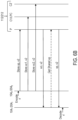
- FIG. 8 is a flowchart for a rebuild process according to one or more embodiments.
- the rebuild process of FIG. 8 can be performed by, for example, memory controller 114 in FIG. 1 or at least one memory controller 214 in FIG. 2 in conjunction with at least one cache controller 106 in FIG. 1 or at least one cache controller 206 in FIG. 2 .
- the memory controller determines that data stored in one or more nodes in a blast zone needs to be reconstructed and stored in one or more nodes from a rebuild pool in at least one memory.
- the determination can be based on, for example, at least one of a useable life expectancy for the one or more nodes and a failure indication from attempting to access data stored in the one or more nodes.
- a cache requesting access to the data can initiate the rebuild process by sending a message to the shared memory or memory unit indicating that a request for the one or more nodes has timed out for requested data or for an acknowledgment that data has been stored in the one or more nodes. In some implementations, this may occur after the requesting cache has attempted at least one retry by resending its request.
- the memory controller may initiate the rebuild process, such as when not being able to read or write data from the one or more nodes, which may follow attempts to error correct the data using ECC or attempts to retry the read or write operation. In such cases, the memory controller may use at least one of a predetermined number of retry attempts and a timeout value for accessing the data.
- the memory controller may also initiate a rebuild of one or more nodes based on life expectancy information, such as at least one of number of read or write operations performed in the one or more nodes, a change in a threshold voltage needed to read or write data in the one or more nodes, a latency in accessing data in the one or more nodes, and/or an error rate in data stored or retrieved from the one or more nodes.
- life expectancy information such as at least one of number of read or write operations performed in the one or more nodes, a change in a threshold voltage needed to read or write data in the one or more nodes, a latency in accessing data in the one or more nodes, and/or an error rate in data stored or retrieved from the one or more nodes.
- the memory controller defers the performance of any new memory requests from caches to access data in the blast zone.
- the blast zone is sized so that the deferring of new memory requests does not significantly delay operation of the system.
- Any new memory requests received from the caches may be buffered in the shared memory or memory unit to be performed after the entire node or nodes have been rebuilt in the case where an LPC node is being rebuilt or after the particular cache line or cache lines of the deferred request has been reconstructed in the rebuilt node(s) in the case where the LPC node is not being rebuilt.
- the memory controller may discard repeated memory requests for the same cache line(s) from the same cache so that the deferred requests can be performed in the order in which they were received after the data has been reconstructed and to conserve space in any buffers that may be used to defer the new requests.
- the performance of at least one memory request is deferred since an initial memory request from a cache may initiate the rebuild process.
- the first memory request that triggers the determination that data stored in the one or more nodes needs to be reconstructed is then considered the first deferred memory request.
- the memory controller designates one or more spare nodes from a rebuild pool of the at least one memory to replace the one or more nodes of the blast zone being rebuilt.
- the designation can be made by changing a mapping, such as a routing table, to replace a physical address or addresses for the one or more nodes being rebuilt with a physical address or addresses for the one or more spare nodes. Since multiple caches and/or the memory controller may initiate the rebuild process as discussed above for block 802 , the memory controller serializes the designation of each spare node by selecting a first spare node in the rebuild pool and disregards additional messages to rebuild the same node.
- erasure decoding is performed using data stored in one or more other nodes in the blast zone to reconstruct the data stored in the one or more nodes being rebuilt.
- the memory controller can recruit caches that request access to data in the blast zone to reconstruct the data for the node or nodes being rebuilt. This improves the efficiency of the rebuild process since the processors instructing the requesting caches would otherwise stall or encounter delays by not having access to data in the blast zone while the node(s) are being rebuilt.
- the memory controller can send a reconstruct message for a cache line to the requesting cache in response to receiving a request from the cache during the rebuild process.
- a cache controller of the cache can then erasure decode the portions or portions of the cache line to be reconstructed using data from the remaining nodes in the blast zone.
- only one cache may end up reconstructing all the data for the rebuilt node(s) if no other caches are sending memory requests during the rebuild process.
- the memory controller or other hardware of the shared memory or memory unit e.g., a hardware accelerator such as a GPU
- the reconstructed data is stored in the one or more spare nodes.
- the cache or caches that have been recruited to reconstruct the data may send the cache line portions as they are reconstructed.
- the memory controller may then update a count or other indicator, such as an indication in the state of the cache line in the LPC node to indicate that reconstruction of the cache line has been completed.
- the memory controller resumes performance of any deferred memory requests in the blast zone.
- the resumption of deferred memory requests may occur after the requested cache line has been reconstructed. In such cases, the performance of certain memory requests may occur while other cache lines are still being reconstructed.
- the resumption of the deferred memory requests may occur after all the cache lines for the blast zone have been reconstructed.
- implementations of the rebuild process of FIG. 8 may differ.
- other implementations may omit the deferral of new memory requests in block 804 where the rebuild process is initiated without receiving a memory request from a cache and no new memory requests are received throughout the rebuild process.
- the memory controller may reconstruct the data on its own or may recruit caches for reconstructing data on a basis other than the origination of memory requests, such as based on a past history of access of the blast zone by the recruited caches.
- the foregoing fault tolerance and memory coherence arrangements and operations can reduce the latency and storage footprint otherwise needed to maintain fault tolerant and coherent data in large-scale systems.
- the independent blast zones storing erasure coded cache lines can provide a lower storage overhead as compared to checkpointing an entire redundant copy of the cache lines.
- the performance penalty for reconstructing data in each independent blast zone is compartmentalized or limited to the blast zone, which can be sized based on an acceptable performance penalty for rebuilding one or more nodes.
- the performance cost in maintaining coherence of the cache lines in large scale systems is also compartmentalized, which generally improves scalability of the system.
- the foregoing fault tolerance and memory coherence operations can significantly reduce downtime in large-scale systems, such as supercomputers and data centers, since the independent blast zones are relatively small and scalable as compared to conventional coherence and fault tolerance methods used for system memory.
- a general purpose processor may be a microprocessor, but in the alternative, the processor may be any conventional processor, controller, microcontroller, or state machine.
- Processor or controller circuitry may also be implemented as a combination of computing devices, e.g., a combination of a DSP and a microprocessor, a plurality of microprocessors, an SoC, one or more microprocessors in conjunction with a DSP core, or any other such configuration.
- a software module may reside in RAM memory, flash memory, ROM memory, EPROM memory, EEPROM memory, registers, hard disk, a removable media, an optical media, or any other form of storage medium known in the art.
- An exemplary storage medium is coupled to processor or controller circuitry such that the processor or controller circuitry can read information from, and write information to, the storage medium.
- the storage medium may be integral to processor or controller circuitry.
- the processor or controller circuitry and the storage medium may reside in an ASIC or an SoC.
Landscapes
- Engineering & Computer Science (AREA)
- Theoretical Computer Science (AREA)
- Physics & Mathematics (AREA)
- General Engineering & Computer Science (AREA)
- General Physics & Mathematics (AREA)
- Computing Systems (AREA)
- Quality & Reliability (AREA)
- Mathematical Physics (AREA)
- Computer Hardware Design (AREA)
- Software Systems (AREA)
- Memory System Of A Hierarchy Structure (AREA)
Abstract
Description
Claims (20)
Priority Applications (1)
| Application Number | Priority Date | Filing Date | Title |
|---|---|---|---|
| US17/853,752 US12189532B2 (en) | 2022-06-29 | 2022-06-29 | Fault tolerance and coherence for shared memory |
Applications Claiming Priority (1)
| Application Number | Priority Date | Filing Date | Title |
|---|---|---|---|
| US17/853,752 US12189532B2 (en) | 2022-06-29 | 2022-06-29 | Fault tolerance and coherence for shared memory |
Publications (2)
| Publication Number | Publication Date |
|---|---|
| US20240004795A1 US20240004795A1 (en) | 2024-01-04 |
| US12189532B2 true US12189532B2 (en) | 2025-01-07 |
Family
ID=89433178
Family Applications (1)
| Application Number | Title | Priority Date | Filing Date |
|---|---|---|---|
| US17/853,752 Active US12189532B2 (en) | 2022-06-29 | 2022-06-29 | Fault tolerance and coherence for shared memory |
Country Status (1)
| Country | Link |
|---|---|
| US (1) | US12189532B2 (en) |
Citations (12)
| Publication number | Priority date | Publication date | Assignee | Title |
|---|---|---|---|---|
| US8954790B2 (en) | 2010-07-05 | 2015-02-10 | Intel Corporation | Fault tolerance of multi-processor system with distributed cache |
| US9280478B2 (en) | 2013-04-26 | 2016-03-08 | Avago Technologies General Ip (Singapore) Pte. Ltd. | Cache rebuilds based on tracking data for cache entries |
| WO2016068870A1 (en) * | 2014-10-28 | 2016-05-06 | Hewlett Packard Enterprise Development Lp | Media controller with coordination buffer |
| US9411730B1 (en) * | 2015-04-02 | 2016-08-09 | International Business Machines Corporation | Private memory table for reduced memory coherence traffic |
| CN103914402B (en) | 2014-04-17 | 2016-08-31 | 华中科技大学 | A kind of reconstruction and optimization method based on correcting and eleting codes caching |
| US10157134B2 (en) | 2016-04-11 | 2018-12-18 | International Business Machines Corporation | Decreasing the data handoff interval for a reserved cache line based on an early indication of a systemwide coherence response |
| US10467139B2 (en) | 2017-12-29 | 2019-11-05 | Oracle International Corporation | Fault-tolerant cache coherence over a lossy network |
| US20200027514A1 (en) * | 2018-07-19 | 2020-01-23 | Micron Technology, Inc. | Using a status indicator in a memory sub-system to detect an event |
| US20210232421A1 (en) | 2020-01-27 | 2021-07-29 | International Business Machines Corporation | Implementing erasure coding with persistent memory |
| US11175984B1 (en) * | 2019-12-09 | 2021-11-16 | Radian Memory Systems, Inc. | Erasure coding techniques for flash memory |
| US20210382858A1 (en) * | 2020-06-05 | 2021-12-09 | Vmware, Inc. | Efficient erasure-coded storage in distributed data systems |
| US20220066876A1 (en) * | 2020-08-27 | 2022-03-03 | Micron Technology, Inc. | Reduced parity data management |
-
2022
- 2022-06-29 US US17/853,752 patent/US12189532B2/en active Active
Patent Citations (12)
| Publication number | Priority date | Publication date | Assignee | Title |
|---|---|---|---|---|
| US8954790B2 (en) | 2010-07-05 | 2015-02-10 | Intel Corporation | Fault tolerance of multi-processor system with distributed cache |
| US9280478B2 (en) | 2013-04-26 | 2016-03-08 | Avago Technologies General Ip (Singapore) Pte. Ltd. | Cache rebuilds based on tracking data for cache entries |
| CN103914402B (en) | 2014-04-17 | 2016-08-31 | 华中科技大学 | A kind of reconstruction and optimization method based on correcting and eleting codes caching |
| WO2016068870A1 (en) * | 2014-10-28 | 2016-05-06 | Hewlett Packard Enterprise Development Lp | Media controller with coordination buffer |
| US9411730B1 (en) * | 2015-04-02 | 2016-08-09 | International Business Machines Corporation | Private memory table for reduced memory coherence traffic |
| US10157134B2 (en) | 2016-04-11 | 2018-12-18 | International Business Machines Corporation | Decreasing the data handoff interval for a reserved cache line based on an early indication of a systemwide coherence response |
| US10467139B2 (en) | 2017-12-29 | 2019-11-05 | Oracle International Corporation | Fault-tolerant cache coherence over a lossy network |
| US20200027514A1 (en) * | 2018-07-19 | 2020-01-23 | Micron Technology, Inc. | Using a status indicator in a memory sub-system to detect an event |
| US11175984B1 (en) * | 2019-12-09 | 2021-11-16 | Radian Memory Systems, Inc. | Erasure coding techniques for flash memory |
| US20210232421A1 (en) | 2020-01-27 | 2021-07-29 | International Business Machines Corporation | Implementing erasure coding with persistent memory |
| US20210382858A1 (en) * | 2020-06-05 | 2021-12-09 | Vmware, Inc. | Efficient erasure-coded storage in distributed data systems |
| US20220066876A1 (en) * | 2020-08-27 | 2022-03-03 | Micron Technology, Inc. | Reduced parity data management |
Also Published As
| Publication number | Publication date |
|---|---|
| US20240004795A1 (en) | 2024-01-04 |
Similar Documents
| Publication | Publication Date | Title |
|---|---|---|
| US10394708B2 (en) | Apparatus and method of damage recovery of storage class memory using repair entry in write cache | |
| US11537512B2 (en) | Asynchronous power loss recovery for memory devices | |
| US11237758B2 (en) | Apparatus and method of wear leveling for storage class memory using address cache | |
| US11714722B2 (en) | Power loss recovery for memory devices | |
| US11704247B2 (en) | Enhanced duplicate write data tracking for cache memory | |
| US20220214971A1 (en) | Sector-based tracking for a page cache | |
| US11392505B2 (en) | Rebuilding logical-to-physical address mapping with limited memory | |
| US12086469B2 (en) | Resiliency and performance for cluster memory | |
| US11907065B2 (en) | Resiliency and performance for cluster memory | |
| US12189532B2 (en) | Fault tolerance and coherence for shared memory | |
| US12216586B2 (en) | Dynamically sized redundant write buffer with sector-based tracking | |
| US12124715B2 (en) | Resiliency and performance for cluster memory | |
| US11698760B2 (en) | Copy and restore of page in byte-addressable chunks of cluster memory | |
| US11397654B2 (en) | Client-assisted phase-based media scrubbing | |
| WO2022240776A1 (en) | Operating memory device in performance mode |
Legal Events
| Date | Code | Title | Description |
|---|---|---|---|
| FEPP | Fee payment procedure |
Free format text: ENTITY STATUS SET TO UNDISCOUNTED (ORIGINAL EVENT CODE: BIG.); ENTITY STATUS OF PATENT OWNER: LARGE ENTITY |
|
| AS | Assignment |
Owner name: WESTERN DIGITAL TECHNOLOGIES, INC., CALIFORNIA Free format text: ASSIGNMENT OF ASSIGNORS INTEREST;ASSIGNORS:VUCINIC, DEJAN;HOFMANN, JACO;LOEWENSTEIN, PAUL;AND OTHERS;REEL/FRAME:060423/0574 Effective date: 20220630 |
|
| AS | Assignment |
Owner name: JPMORGAN CHASE BANK, N.A., ILLINOIS Free format text: PATENT COLLATERAL AGREEMENT - DDTL LOAN AGREEMENT;ASSIGNOR:WESTERN DIGITAL TECHNOLOGIES, INC.;REEL/FRAME:067045/0156 Effective date: 20230818 Owner name: JPMORGAN CHASE BANK, N.A., ILLINOIS Free format text: PATENT COLLATERAL AGREEMENT - A&R LOAN AGREEMENT;ASSIGNOR:WESTERN DIGITAL TECHNOLOGIES, INC.;REEL/FRAME:064715/0001 Effective date: 20230818 |
|
| STPP | Information on status: patent application and granting procedure in general |
Free format text: FINAL REJECTION MAILED |
|
| STPP | Information on status: patent application and granting procedure in general |
Free format text: RESPONSE AFTER FINAL ACTION FORWARDED TO EXAMINER |
|
| STPP | Information on status: patent application and granting procedure in general |
Free format text: ADVISORY ACTION MAILED |
|
| STPP | Information on status: patent application and granting procedure in general |
Free format text: DOCKETED NEW CASE - READY FOR EXAMINATION |
|
| STPP | Information on status: patent application and granting procedure in general |
Free format text: NON FINAL ACTION MAILED |
|
| STPP | Information on status: patent application and granting procedure in general |
Free format text: RESPONSE TO NON-FINAL OFFICE ACTION ENTERED AND FORWARDED TO EXAMINER |
|
| STPP | Information on status: patent application and granting procedure in general |
Free format text: NOTICE OF ALLOWANCE MAILED -- APPLICATION RECEIVED IN OFFICE OF PUBLICATIONS |
|
| STPP | Information on status: patent application and granting procedure in general |
Free format text: PUBLICATIONS -- ISSUE FEE PAYMENT VERIFIED |
|
| STCF | Information on status: patent grant |
Free format text: PATENTED CASE |