US12178043B2 - Nonvolatile memory device - Google Patents
Nonvolatile memory device Download PDFInfo
- Publication number
- US12178043B2 US12178043B2 US17/232,500 US202117232500A US12178043B2 US 12178043 B2 US12178043 B2 US 12178043B2 US 202117232500 A US202117232500 A US 202117232500A US 12178043 B2 US12178043 B2 US 12178043B2
- Authority
- US
- United States
- Prior art keywords
- word line
- line cut
- stacked structure
- filling
- stacked
- Prior art date
- Legal status (The legal status is an assumption and is not a legal conclusion. Google has not performed a legal analysis and makes no representation as to the accuracy of the status listed.)
- Active, expires
Links
Images


Classifications
-
- G—PHYSICS
- G11—INFORMATION STORAGE
- G11C—STATIC STORES
- G11C16/00—Erasable programmable read-only memories
- G11C16/02—Erasable programmable read-only memories electrically programmable
- G11C16/04—Erasable programmable read-only memories electrically programmable using variable threshold transistors, e.g. FAMOS
- G11C16/0483—Erasable programmable read-only memories electrically programmable using variable threshold transistors, e.g. FAMOS comprising cells having several storage transistors connected in series
-
- G—PHYSICS
- G11—INFORMATION STORAGE
- G11C—STATIC STORES
- G11C8/00—Arrangements for selecting an address in a digital store
- G11C8/14—Word line organisation; Word line lay-out
-
- H—ELECTRICITY
- H10—SEMICONDUCTOR DEVICES; ELECTRIC SOLID-STATE DEVICES NOT OTHERWISE PROVIDED FOR
- H10B—ELECTRONIC MEMORY DEVICES
- H10B41/00—Electrically erasable-and-programmable ROM [EEPROM] devices comprising floating gates
- H10B41/10—Electrically erasable-and-programmable ROM [EEPROM] devices comprising floating gates characterised by the top-view layout
-
- H—ELECTRICITY
- H10—SEMICONDUCTOR DEVICES; ELECTRIC SOLID-STATE DEVICES NOT OTHERWISE PROVIDED FOR
- H10B—ELECTRONIC MEMORY DEVICES
- H10B41/00—Electrically erasable-and-programmable ROM [EEPROM] devices comprising floating gates
- H10B41/20—Electrically erasable-and-programmable ROM [EEPROM] devices comprising floating gates characterised by three-dimensional [3D] arrangements, e.g. with cells on different height levels
- H10B41/23—Electrically erasable-and-programmable ROM [EEPROM] devices comprising floating gates characterised by three-dimensional [3D] arrangements, e.g. with cells on different height levels with source and drain on different levels, e.g. with sloping channels
- H10B41/27—Electrically erasable-and-programmable ROM [EEPROM] devices comprising floating gates characterised by three-dimensional [3D] arrangements, e.g. with cells on different height levels with source and drain on different levels, e.g. with sloping channels the channels comprising vertical portions, e.g. U-shaped channels
-
- H—ELECTRICITY
- H10—SEMICONDUCTOR DEVICES; ELECTRIC SOLID-STATE DEVICES NOT OTHERWISE PROVIDED FOR
- H10B—ELECTRONIC MEMORY DEVICES
- H10B41/00—Electrically erasable-and-programmable ROM [EEPROM] devices comprising floating gates
- H10B41/30—Electrically erasable-and-programmable ROM [EEPROM] devices comprising floating gates characterised by the memory core region
- H10B41/35—Electrically erasable-and-programmable ROM [EEPROM] devices comprising floating gates characterised by the memory core region with a cell select transistor, e.g. NAND
-
- H—ELECTRICITY
- H10—SEMICONDUCTOR DEVICES; ELECTRIC SOLID-STATE DEVICES NOT OTHERWISE PROVIDED FOR
- H10B—ELECTRONIC MEMORY DEVICES
- H10B43/00—EEPROM devices comprising charge-trapping gate insulators
- H10B43/10—EEPROM devices comprising charge-trapping gate insulators characterised by the top-view layout
-
- H—ELECTRICITY
- H10—SEMICONDUCTOR DEVICES; ELECTRIC SOLID-STATE DEVICES NOT OTHERWISE PROVIDED FOR
- H10B—ELECTRONIC MEMORY DEVICES
- H10B43/00—EEPROM devices comprising charge-trapping gate insulators
- H10B43/20—EEPROM devices comprising charge-trapping gate insulators characterised by three-dimensional [3D] arrangements, e.g. with cells on different height levels
- H10B43/23—EEPROM devices comprising charge-trapping gate insulators characterised by three-dimensional [3D] arrangements, e.g. with cells on different height levels with source and drain on different levels, e.g. with sloping channels
- H10B43/27—EEPROM devices comprising charge-trapping gate insulators characterised by three-dimensional [3D] arrangements, e.g. with cells on different height levels with source and drain on different levels, e.g. with sloping channels the channels comprising vertical portions, e.g. U-shaped channels
-
- H—ELECTRICITY
- H10—SEMICONDUCTOR DEVICES; ELECTRIC SOLID-STATE DEVICES NOT OTHERWISE PROVIDED FOR
- H10B—ELECTRONIC MEMORY DEVICES
- H10B43/00—EEPROM devices comprising charge-trapping gate insulators
- H10B43/30—EEPROM devices comprising charge-trapping gate insulators characterised by the memory core region
- H10B43/35—EEPROM devices comprising charge-trapping gate insulators characterised by the memory core region with cell select transistors, e.g. NAND
-
- H—ELECTRICITY
- H10—SEMICONDUCTOR DEVICES; ELECTRIC SOLID-STATE DEVICES NOT OTHERWISE PROVIDED FOR
- H10W—GENERIC PACKAGES, INTERCONNECTIONS, CONNECTORS OR OTHER CONSTRUCTIONAL DETAILS OF DEVICES COVERED BY CLASS H10
- H10W20/00—Interconnections in chips, wafers or substrates
- H10W20/01—Manufacture or treatment
- H10W20/031—Manufacture or treatment of conductive parts of the interconnections
- H10W20/056—Manufacture or treatment of conductive parts of the interconnections by filling conductive material into holes, grooves or trenches
-
- H—ELECTRICITY
- H10—SEMICONDUCTOR DEVICES; ELECTRIC SOLID-STATE DEVICES NOT OTHERWISE PROVIDED FOR
- H10W—GENERIC PACKAGES, INTERCONNECTIONS, CONNECTORS OR OTHER CONSTRUCTIONAL DETAILS OF DEVICES COVERED BY CLASS H10
- H10W90/00—Package configurations
Definitions
- Inventive concepts relate to a nonvolatile memory device, and more particularly, to a three-dimensional (3D) nonvolatile memory device.
- a 3D memory device including a plurality of gate layers stacked on a substrate and a channel passing through the plurality of gate layers has been proposed. Because the degree of integration of the 3D memory device may be improved by increasing the number of gate layers to be stacked, the 3D memory device may be advantageous in improving the degree of integration.
- Inventive concepts provide a nonvolatile memory device having a simplified process and/or reduced cost.
- a nonvolatile memory device may include a substrate; a first stacked structure including a plurality of first gate layers and a plurality of first interlayer insulating layers alternately stacked on the substrate; a second stacked structure including a plurality of second gate layers and a plurality of second interlayer insulating layers alternately stacked on the first stacked structure; a channel structure including a first portion passing through the first stacked structure and a second portion passing through the second stacked structure; and a filling structure including a first portion passing through the first stacked structure and extending in a first horizontal direction and a second portion passing through the second stacked structure and extending in the first horizontal direction.
- a diameter of an upper end of the first portion of the channel structure may be greater than a diameter of a lower end of the second portion of the channel structure.
- a width of an upper end of the first portion of the filling structure in a second horizontal direction may be greater than a width in the second horizontal direction of the lower end of the second portion of the filling structure.
- the upper end of the first portion of the filling structure may be at a same height as the upper end of the first portion of the channel structure.
- a nonvolatile memory device may include a substrate; a first stacked structure including a plurality of first gate layers and a plurality of first interlayer insulating layers alternately stacked on the substrate; a second stacked structure including a plurality of second gate layers and a plurality of second interlayer insulating layers alternately stacked on the first stacked structure; a channel structure including a first portion passing through the first stacked structure and a second portion passing through the second stacked structure; and a filling structure passing through at least a portion of the first stacked structure and the second stacked structure.
- the filling structure may extend in a first horizontal direction.
- the filling structure may include a first portion, a second portion, and a third portion.
- the first portion of the filling structure may pass through the first stacked structure and extend in the first horizontal direction.
- the second portion of the filling structure may be on the first portion of the filling structure, pass through the second stacked structure, and extend in the first horizontal direction.
- the third portion of the filling structure may be on the first portion of the filling structure, pass through the second stacked structure, and extend in the first horizontal direction.
- the third portion of the filling structure may be spaced apart from the second portion of the filling structure in the first horizontal direction.
- An upper end of the first portion of the filling structure may be at a same height as an upper end of the first portion of the channel structure.
- a nonvolatile memory device may include a substrate; a first stacked structure including a plurality of first gate layers and a plurality of first interlayer insulating layers alternately stacked on the substrate; a second stacked structure including a plurality of second gate layers and a plurality of second interlayer insulating layers alternately stacked on the first stacked structure; a channel structure; and a first filling structure.
- the first stacked structure may define a first channel hole and a first word line cut passing through the first stacked structure.
- the first word line cut may extend in a first horizontal direction.
- the second stacked structure may define a second channel hole and a second word line cut passing through the second stacked structure.
- the second word line cut may extend in the first horizontal direction.
- the channel structure may be in the first channel hole and the second channel hole.
- the channel structure may pass through the first stacked structure and the second stacked structure.
- the channel structure may extend partially into the substrate.
- the first filling structure may be in the first word line cut and the second word line cut.
- the first filling structure may pass through the first stacked structure and the second stacked structure.
- the first filling structure may extend partially into the substrate.
- a height of a lower end of the first word line cut may be lower than a height of a lower end of the first channel hole.
- An upper end of the first word line cut may be at a same height as an upper end of the first channel hole.
- FIG. 1 is a plan view of a nonvolatile memory device according to embodiments
- FIG. 2 is a perspective view of area R 1 of FIG. 1 ;
- FIG. 3 is a cross-sectional view taken along line A-A′ of FIG. 1 ;
- FIG. 4 A is an enlarged cross-sectional view of area R 2 a of FIG. 3 ;
- FIG. 4 B is an enlarged cross-sectional view of area R 2 b of FIG. 3 ;
- FIG. 5 is a cross-sectional view of a nonvolatile memory device according to embodiments.
- FIG. 6 is a cross-sectional view of a nonvolatile memory device according to embodiments.
- FIG. 7 is a cross-sectional view of a nonvolatile memory device according to embodiments.
- FIG. 8 is a cross-sectional view of a nonvolatile memory device according to embodiments.
- FIG. 9 is a cross-sectional view of a nonvolatile memory device according to embodiments.
- FIGS. 10 A to 10 G and 10 I to 10 K are cross-sectional views illustrating a method of manufacturing a nonvolatile memory device, according to embodiments
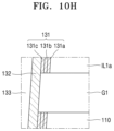
- FIG. 10 H is an enlarged cross-sectional view of area R 3 of FIG. 10 G ;
- FIG. 11 is a cross-sectional view illustrating a method of manufacturing a nonvolatile memory device, according to embodiments.
- FIG. 12 is a schematic view of an electronic system including a nonvolatile memory device according to embodiments.
- FIG. 13 is a perspective view of an electronic system including a nonvolatile memory device according to embodiments.
- FIG. 14 is a cross-sectional view of semiconductor packages according to embodiments.
- FIG. 1 is a plan view of a nonvolatile memory device 100 according to embodiments.
- FIG. 2 is a perspective view schematically illustrating area R 1 of FIG. 1 .
- FIG. 3 is a cross-sectional view taken along line A-A′ of FIG. 1 .
- FIG. 4 A is an enlarged cross-sectional view of area R 2 a of FIG. 3 .
- FIG. 4 B is an enlarged cross-sectional view of area R 2 b of FIG. 3 .
- the nonvolatile memory device 100 may include a substrate 110 , a first stacked structure M 1 on the substrate 110 , a second stacked structure M 2 on the first stacked structure M 1 , a channel structure 130 passing through the first stacked structure M 1 and the second stacked structure M 2 , a first filling structure F 1 , and a second filling structure F 2 .
- the substrate 110 may include a cell area CELL and a step area PR surrounding the cell area CELL.
- the first stacked structure M 1 may be on the cell area CELL and the step area PR of the substrate 110 .
- the second stacked structure M 2 may be on the first stacked structure M 1 .
- a portion of the first stacked structure M 1 and the second stacked structure M 2 on the step area PR may have a step shape. That is, the higher gate layers G 1 a to G 1 d and G 2 a to G 2 d are, the smaller the plane area may be. For example, a less planar area of the uppermost gate layer G 2 d may be less than that of the lower gate layer G 2 c.
- the substrate 110 may include a semiconductor material, such as a Group IV semiconductor material, a Group III-V semiconductor material, a Group II-VI semiconductor material, or a combination thereof.
- the Group IV semiconductor material may include, for example, silicon (Si), germanium (Ge), or a combination thereof.
- the Group III-V semiconductor material may include, for example, gallium arsenide (GaAs), indium phosphorus (InP), gallium phosphorus (GaP), indium arsenic (InAs), indium antimony (InSb), indium gallium arsenide (InGaAs), or a combination thereof.
- the Group II-VI semiconductor material may include, for example, zinc telluride (ZnTe), cadmium sulfide (CdS), or a combination thereof.
- the substrate 110 may be a bulk wafer or an epitaxial layer.
- the first stacked structure M 1 may include a plurality of first gate layers G 1 a to G 1 d and a plurality of first interlayer insulating layers IL 1 a to IL 1 e alternately stacked on the substrate 110 .
- FIGS. 1 to 3 show that the first stacked structure M 1 includes four first gate layers G 1 a to G 1 d and five first interlayer insulating layers IL 1 a to IL 1 e , but the number of first gate layers and the number of first interlayer insulating layers included in the first stacked structure M 1 may be different than 4 and 5, respectively, such as greater than 4 and 5, respectively.
- the second stacked structure M 2 may include a plurality of second gate layers G 2 a to G 2 d and a plurality of second interlayer insulating layers IL 2 a to IL 2 e alternately stacked on the first stacked structure M 1 .
- FIGS. 1 to 3 show that the second stacked structure M 2 includes four second gate layers G 2 a to G 2 d and five second interlayer insulating layers IL 2 a to IL 2 e , but the number of second gate layers and the number of second interlayer insulating layers included in the second stacked structure M 2 may be different than 4 and 5, respectively, such as greater than 4 and 5, respectively.
- the number of first gate electrodes included in the first stacked structure M 1 may be different from the number of second gate electrodes included in the second stacked structure M 2
- the number of first interlayer insulating layers included in the first stacked structure M 1 may be different from the number of second interlayer insulating layers included in the second stacked structure M 2 .
- a thickness T 1 U of the uppermost interlayer insulating layer IL 1 e from among the plurality of first interlayer insulating layers IL 1 a to IL 1 e may be greater than a thickness T 1 of one (e.g., IL 1 d ) of the plurality of first interlayer insulating layers IL 1 a to IL 1 e .
- a thickness T 2 L of the lowermost interlayer insulating layer IL 2 a from among the plurality of second interlayer insulating layers IL 2 a to IL 2 e may be greater than a thickness T 2 of one (e.g., IL 2 b ) of the plurality of second interlayer insulating layers IL 2 a to IL 2 e.
- the plurality of first gate layers G 1 a to G 1 d and the plurality of second gate layers G 2 a to G 2 d may include tungsten (W), copper (Cu), silver (Ag), gold (Au), aluminum (Al), or a combination thereof, but may include a conductive material, though not limited thereto.
- the first gate layers G 1 a to G 1 d and the second gate layers G 2 a to G 2 d may include titanium (Ti), tantalum (Ta), titanium nitride (TiN), tantalum nitride (TaN), or a combination thereof to limit and/or prevent diffusion of the conductive material into the plurality of first interlayer insulating layers IL 1 a to IL 1 e and the plurality of second interlayer insulating layers IL 2 a to IL 2 e , but may further include a barrier material, though not limited thereto.
- the plurality of first interlayer insulating layers IL 1 a to IL 1 e and the plurality of second interlayer insulating layers IL 2 a to IL 2 e may include, for example, silicon oxide, silicon nitride, a low dielectric (low-K) material, or a combination thereof.
- the low-K material is a material having a lower dielectric constant than that of silicon oxide, and may include, for example, phosphosilicate glass (PSG), borophosphosilicate glass (BPSG), fluorosilicate glass (FSG), organosilicate glass (OSG), spin-on-glass (SOG), spin-on-polymer, or a combination thereof.
- the channel structure 130 may pass through portions of the first stacked structure M 1 and the second stacked structure M 2 on the cell area CELL.
- the channel structure 130 may include a first portion 130 a passing through the first stacked structure M 1 and a second portion 130 b passing through the second stacked structure M 2 .
- the first portion 130 a of the channel structure 130 may be in a first channel hole CHa passing through the first stacked structure M 1
- the second portion 130 b of the channel structure 130 may be in a second channel hole CHb passing through the stacked structure M 2
- the second portion 130 b of the channel structure 130 may be on the first portion 130 a of the channel structure 130 .
- a diameter D 1 of an upper end of the first portion 130 a of the channel structure 130 may be greater than a diameter D 2 of a lower end of the second portion 130 b of the channel structure 130 .
- the channel structure 130 may include a gate insulating layer 131 in the first channel hole CHa and the second channel hole CHb and a channel layer 132 on the gate insulating layer 131 .
- the channel structure 130 may further include a filling insulating layer 133 in a space surrounded by the channel layer 132 and a channel pad 134 on the filling insulating layer 133 .
- the gate insulating layer 131 may extend along a side surface and bottom of the first channel hole CHa and along a side surface of the second channel hole CHb. In some embodiments, unlike the example shown in FIG. 3 , the gate insulating layer 131 may further extend between the second channel hole CHb and the channel pad 134 . As shown in FIG. 4 A , the gate insulating layer 131 may include a blocking insulating layer 131 a , a charge storage layer 131 b , and a tunneling insulating layer 131 c that are sequentially stacked in the first channel hole CHa and the second channel hole CHb.
- the blocking insulating layer 131 a may include, for example, silicon oxide, silicon nitride, metal oxide having a higher dielectric constant than silicon oxide, or a combination thereof.
- the metal oxide may include, for example, hafnium oxide, aluminum oxide, zirconium oxide, tantalum oxide, or a combination thereof.
- the charge storage layer 131 b may include, for example, silicon nitride, boron nitride, polysilicon, or a combination thereof.
- the tunneling insulating layer 131 c may include, for example, metal oxide or silicon oxide.
- the blocking insulating layer 131 a , the charge storage layer 131 b , and the tunneling insulating layer 131 c may include oxide, nitride, and oxide, respectively.
- the channel layer 132 may extend along the gate insulating layer 131 .
- the channel layer 132 may include a semiconductor material such as a Group IV semiconductor material, a Group III-V semiconductor material, or a Group II-VI semiconductor material.
- the channel layer 132 may include polysilicon.
- the filling insulating layer 133 may include an insulating material that may include, for example, silicon nitride, silicon oxide, or a combination thereof. In some embodiments, the filling insulating layer 133 may include silicon oxide.
- the channel pad 134 is above the second channel hole CHb and may contact the channel layer 132 .
- the channel pad 134 may include a semiconductor material such as Si, Ge, and Si—Ge; a metallic material such as W, Ti, Al, Cu, Au, and Ag; a metal nitride such as TiN or TaN; or a conductive material such as a combination thereof.
- the channel pad 134 may include polysilicon.
- the first filling structure F 1 may include a first portion Fla passing through the first stacked structure M 1 and a second portion F 1 b passing through the second stacked structure M 2 .
- the first portion Fla of the first filling structure F 1 may be in a first word line cut WC 1 a passing through the first stacked structure M 1 .
- the second portion F 1 b of the first filling structure F 1 may be in a second word line cut WC 1 b passing through the second stacked structure M 2 .
- the second portion F 1 b of the first filling structure F 1 is on the first portion Fla of the first filling structure F 1 and may extend along the first filling structure F 1 .
- a width W 1 of an upper end of the first portion Fla of the first filling structure F 1 in a second horizontal direction (Y direction) may be greater than a width W 2 of a lower end of the second portion F 1 b of the first filling structure F 1 in the second horizontal direction (Y direction).
- the first portion Fla of the first filling structure F 1 may extend in a first horizontal direction (X direction). That is, the first word line cut WC 1 a may extend in the first horizontal direction (X direction).
- the first portion Fla of the first filling structure F 1 may completely pass through the first stacked structure M 1 in the first horizontal direction (X direction). That is, the first word line cut WC 1 a may completely pass through the first stacked structure M 1 in the first horizontal direction (X direction).
- the second portion F 1 b of the first filling structure F 1 may extend in the first horizontal direction (X direction). That is, the second word line cut WC 1 b may extend in the first horizontal direction (X direction).
- the second portion F 1 b of the first filling structure F 1 may completely pass through the second stacked structure M 2 in the first horizontal direction (X direction). That is, the second word line cut WC 1 b may completely pass through the second stacked structure M 2 in the first horizontal direction (X direction).
- a length L 1 of the first filling structure F 1 in the first horizontal direction (X direction) may be greater than a width W 5 of the first filling structure F 1 in the second horizontal direction (Y direction).
- the second filling structure F 2 may include a first portion F 2 a passing through the first stacked structure M 1 , a second portion F 2 b passing through the second stacked structure M 2 , and a third portion F 2 c passing through the second stacked structure M 2 .
- the first portion F 2 a of the second filling structure F 2 may be in a third word line cut WC 2 a passing through the first stacked structure M 1 .
- the second portion F 2 b of the second filling structure F 2 may be in a fourth word line cut WC 2 b passing through the second stacked structure M 2 .
- the third portion F 2 c of the second filling structure F 2 may be in a fifth word line cut WC 2 c passing through the second stacked structure M 2 .
- the second portion F 2 b and the third portion F 2 c of the second filling structure F 2 may be on the first portion F 2 a of the second filling structure F 2 .
- the first portion F 2 a of the second filling structure F 2 may extend in the first horizontal direction (X direction). That is, the third word line cut WC 2 a may extend in the first horizontal direction (X direction).
- the first portion F 2 a of the second filling structure F 2 may completely pass through the first stacked structure M 1 in the first horizontal direction (X direction). That is, the third word line cut WC 2 a may completely pass through the first stacked structure M 1 in the first horizontal direction (X direction).
- the second portion F 2 b and the third portion F 2 c of the second filling structure F 2 may extend in the first horizontal direction (X direction). That is, the fourth word line cut WC 2 b and the fifth word line cut WC 2 c may extend in the first horizontal direction (X direction).
- the second portion F 2 b and the third portion F 2 c of the second filling structure F 2 may partially pass through the second stacked structure M 2 in the first horizontal direction (X direction). That is, the fourth word line cut WC 2 b and the fifth word line cut WC 2 c may only partially pass through the second stacked structure M 2 in the first horizontal direction (X direction).
- the second portion F 2 b of the second filling structure F 2 may be apart from the third portion F 2 c of the second filling structure F 2 in the first horizontal direction (X direction).
- a length L 2 of the first portion F 2 a of the second filling structure F 2 in the first horizontal direction (X direction) may be greater than a length L 3 of the second portion F 2 b of the second filling structure F 2 in the first horizontal direction (X direction).
- the third word line cut WC 2 a may be apart from the first word line cut WC 1 a in the second horizontal direction (Y direction).
- the fourth word line cut WC 2 b may be apart from the second word line cut WC 1 b in the second horizontal direction (Y direction).
- the fifth word line cut WC 2 c may be apart from the second word line cut WC 1 b in the second horizontal direction (Y direction).
- the fourth word line cut WC 2 b may be apart from the fifth word line cut WC 2 c in the first horizontal direction (X direction).
- the fourth word line cut WC 2 b and the fifth word line cut WC 2 c may be connected to the third word line cut WC 2 a.
- the first stacked structure M 1 may include a first sub-stack SS 1 , a second sub-stack SS 2 , and a third sub-stack SS 3 .
- the first sub-stack SS 1 and the second sub-stack SS 2 may be apart from each other by the first portion Fla of the first filling structure F 1 .
- the second sub-stack SS 2 and the third sub-stack SS 3 may be apart from each other by the first portion F 2 a of the second filling structure F 2 .
- the second stacked structure M 2 may include a fourth sub-stack SS 4 , a fifth sub-stack SS 5 , a sixth sub-stack SS 6 , and a connection stack CS.
- the fourth sub-stack SS 4 , the fifth sub-stack SS 5 , and the sixth sub-stack SS 6 may be on the first sub-stack SS 1 , the second sub-stack SS 2 , and the third sub-stack SS 3 , respectively.
- the fourth sub-stack SS 4 and the fifth sub-stack SS 5 may be apart from each other by the second portion F 1 b of the first filling structure F 1 .
- the connection stack CS may connect the fifth sub-stack SS 5 to the sixth sub-stack SS 6 .
- the connection stack CS may be on the first portion F 2 a of the second filling structure F 2 .
- the second portion F 2 b and the third portion F 2 c of the second filling structure F 2 may be apart from each other by the connection stack CS.
- the connection stack CS may limit and/or prevent the fifth sub-stack SS 5 and the sixth sub-stack SS 6 from tilting during a manufacturing process of the nonvolatile memory device 100 .
- the first filling structure F 1 and the second filling structure F 2 may include an insulating material that may include, for example, silicon oxide, silicon nitride, a low-K material, or a combination thereof.
- the upper end of the first portion Fla of the first filling structure F 1 may be at a same height H 1 as the upper end of the first portion 130 a of the channel structure 130 .
- the height H 1 refers to a distance in a vertical direction (Z direction) from a flat bottom surface of the substrate 110 .
- an upper end of the first word line cut WC 1 a may be at the same height H 1 as an upper end of the first channel hole CHa.
- the upper end of the first portion Fla of the first filling structure F 1 may be at the same height H 1 as an upper surface of the uppermost interlayer insulating layer IL 1 e from among the plurality of first interlayer insulating layers IL 1 a to IL 1 e .
- the upper end of the first portion Fla of the first filling structure F 1 , the upper end of the first portion 130 a of the channel structure 130 , and the upper surface of the uppermost interlayer insulating layer IL 1 e may lie on the same virtual surface.
- An upper end of the first portion F 2 a of the second filling structure F 2 may be at the same height H 1 as the upper end of the first portion 130 a of the channel structure 130 .
- an upper end of the third word line cut WC 2 a may be at the same height H 1 as the upper end of the first channel hole CHa.
- the upper end of the first portion F 2 a of the second filling structure F 2 may be at the same height H 1 as the upper surface of the uppermost interlayer insulating layer IL 1 e from among the plurality of first interlayer insulating layers IL 1 a to IL 1 e .
- the upper end of the first portion F 2 a of the second filling structure F 2 , the upper end of the first portion 130 a of the channel structure 130 , and the upper surface of the uppermost interlayer insulating layer IL 1 e may lie on the same virtual surface.
- the nonvolatile memory device 100 may further include a lower conductive layer 120 between the substrate 110 and the first stacked structure M 1 .
- the channel structure 130 , the first filling structure F 1 , the second filling structure F 2 , the first word line cut WC 1 a , the second filling structure F 2 , and the third word line cut WC 2 a may further pass through the lower conductive layer 120 .
- the channel structure 130 , the first channel hole CHa, the first filling structure F 1 , the first word line cut WC 1 a , the second filling structure F 2 , and the third word line cut WC 2 a may further partially pass through the substrate 110 .
- a height H 4 of a lower end of the first word line cut WC 1 a may be less than a height H 3 of a lower end of the first channel hole CHa. That is, the height H 4 of a lower end of the first filling structure F 1 may be less than the height H 3 of a lower end of the channel structure 130 .
- the height H 4 of a lower end of the third word line cut WC 2 a may be less than the height H 3 of the lower end of the first channel hole CHa. That is, the height H 4 of a lower end of the first portion F 2 a of the second filling structure F 2 may be less than the height H 3 of a lower end of the first portion 130 a of the channel structure 130 .
- the lower conductive layer 120 may pass through the gate insulating layer 131 and contact the channel layer 132 .
- the lower conductive layer 120 may include a metal such as W, Al, Au, Ag, or Cu; a metal nitride such as TiN, molybdenum nitride (MoN), or TaN; a semiconductor material such as Si, Ge, or Si—Ge; or a combination thereof.
- the lower conductive layer 120 may include polysilicon.
- the nonvolatile memory device 100 may further include the second stacked structure M 2 and an upper insulating layer ILu on the channel structure 130 .
- the first filling structure F 1 may further pass through the upper insulating layer ILu.
- the first filling structure F 1 may further include a third portion F 1 c passing through the upper insulating layer ILu.
- the third portion F 1 c of the first filling structure F 1 may be in a sixth word line cut WC 1 c passing through the upper insulating layer ILu.
- the third portion F 1 c of the first filling structure F 1 may be on the second portion F 1 b of the first filling structure F 1 .
- the upper insulating layer ILu may include, for example, an insulating material that may include silicon oxide, silicon nitride, a low-K material, or a combination thereof.
- a width W 3 of an upper end of the second portion F 1 b of the first filling structure F 1 in the second horizontal direction (Y direction) may be greater than a width W 4 of an upper end of the third portion F 1 c of the first filling structure F 1 in the second horizontal direction (Y direction).
- an upper end of the second portion F 1 b of the first filling structure F 1 may be at a same height H 2 as an upper end of the channel structure 130 .
- an upper surface of the uppermost interlayer insulating layer IL 2 e from among the plurality of second interlayer insulating layers IL 2 a to IL 2 e may be at the same height as the upper end of the second portion F 1 b of the first filling structure F 1 .
- the upper surface of the channel structure 130 , the upper end of the second portion F 1 b of the first filling structure F 1 , and the upper surface of the uppermost interlayer insulating layer IL 2 e may lie on the same virtual surface.
- FIG. 5 is a cross-sectional view of a nonvolatile memory device 100 - 1 according to embodiments.
- FIG. 5 differs between the nonvolatile memory device 100 - 1 illustrated in FIG. 5 and the nonvolatile memory device 100 illustrated in FIG. 3 will be described.
- the nonvolatile memory device 100 - 1 may include a first filling structure F 1 - 1 .
- the first filling structure F 1 - 1 may include a second portion F 1 b - 1 passing through the second stacked structure M 2 , and a third portion F 1 c - 1 passing through the upper insulating layer ILu.
- the second portion F 1 b - 1 of the first filling structure F 1 - 1 may be in a second word line cut WC 1 b - 1 passing through the second stacked structure M 2 .
- the third portion F 1 c - 1 of the first filling structure F 1 - 1 may be in a sixth word line cut WC 1 c - 1 passing through the upper insulating layer ILu.
- the third portion F 1 c - 1 of the first filling structure F 1 - 1 may partially further pass through the second stacked structure M 2 . That is, the sixth word line cut WC 1 c - 1 may further partially pass through the second stacked structure M 2 .
- a height H 5 of an upper end of the second portion F 1 b - 1 of the first filling structure F 1 - 1 may be less than the height H 2 of an upper end of the second portion 130 b of the channel structure 130 . That is, the height H 5 of an upper end of the second word line cut WC 1 b - 1 may be less than the height H 2 of the upper end of the second portion 130 b of the channel structure 130 .
- the height H 5 of the upper end of the second portion F 1 b - 1 of the first filling structure F 1 - 1 may be less than the height H 2 of the upper surface of the uppermost insulating layer IL 2 e from among the plurality of second interlayer insulating layers IL 2 a to IL 2 e . That is, the height H 5 of the upper end of the second word line cut WC 1 b - 1 may be less than the height H 2 of the upper surface of the uppermost insulating layer IL 2 e.
- a width W 6 of the upper end of the second portion F 1 b - 1 of the first filling structure F 1 - 1 in the second horizontal direction (Y direction) may be less than the width W 5 of a lower end of the third portion F 1 c - 1 of the first filling structure F 1 - 1 in the second horizontal direction (Y direction). Accordingly, due to over-etching, the sixth word line cut WC 1 c - 1 may be formed to partially pass through the second stacked structure M 2 .
- FIG. 6 is a cross-sectional view of a nonvolatile memory device 100 - 2 according to embodiments.
- FIG. 6 differences between the nonvolatile memory device 100 - 2 illustrated in FIG. 6 and the nonvolatile memory device 100 illustrated in FIG. 3 will be described.
- the nonvolatile memory device 100 - 2 may not include the lower conductive layer 120 (see FIG. 3 ).
- the first stacked structure M 1 may be formed directly on the substrate 110 .
- the nonvolatile memory device 100 - 2 may include a channel structure 130 - 2 .
- the channel structure 130 - 2 may include a first portion 130 a - 2 passing through the first stacked structure M 1 .
- the first portion 130 a - 2 of the channel structure 130 - 2 may be in a first channel hole CHa- 2 passing through the first stacked structure M 1 .
- the channel structure 130 - 2 may include a gate insulating layer 131 - 2 in the first channel hole CHa- 2 and the second channel hole CHb.
- the gate insulating layer 131 - 2 may not cover the bottom of the first channel hole CHa- 2 .
- the channel layer 132 may directly contact the substrate 110 .
- the nonvolatile memory device 100 - 2 may include a first filling structure F 1 - 2 .
- the first filling structure F 1 - 2 may include a first portion Fla- 2 passing through the first stacked structure M 1 .
- the first portion Fla- 2 of the first filling structure F 1 - 2 may be in a first word line cut WC 1 a - 2 passing through the first stacked structure M 1 .
- the nonvolatile memory device 100 - 2 may include a second filling structure.
- the second filling structure may include a first portion F 2 a - 2 passing through the first stacked structure M 1 .
- the first portion F 2 a - 2 of the second filling structure may be in a third word line cut WC 2 a - 2 passing through the first stacked structure M 1 .
- a lower end of the first portion F 1 a - 2 of the first filling structure F 1 - 2 may be at a same height H 6 as a lower end of the first portion 130 a - 2 of the channel structure 130 . That is, a lower end of the first word line cut WC 1 a - 2 may be at the same height H 6 as a lower end of the first channel hole CHa- 2 .
- a lower end of the first portion F 2 a - 2 of the second filling structure may be at the same height H 6 as the lower end of the first portion 130 a - 2 of the channel structure 130 . That is, a lower end of the third word line cut WC 2 a - 2 may be at the same height H 6 as the lower end of the first channel hole CHa- 2 .
- FIG. 7 is a cross-sectional view of a nonvolatile memory device 100 - 3 according to embodiments.
- FIG. 7 differences between the nonvolatile memory device 100 - 3 illustrated in FIG. 7 and the nonvolatile memory device 100 illustrated in FIG. 3 will be described.
- the nonvolatile memory device 100 - 3 may include a first filling structure F 1 - 3 and a second filling structure F 2 - 3 .
- Each of the first filling structure F 1 - 3 and the second filling structure F 2 - 3 may include an insulating layer 141 and a conductive layer 142 surrounded by the insulating layer 141 .
- the conductive layer 142 may pass through the first stacked structure M 1 and the second stacked structure M 2 . In some embodiments, the conductive layer 142 may further pass through the upper insulating layer ILu. In some embodiments, the conductive layer 142 may further pass through the lower conductive layer 120 . In some embodiments, the conductive layer 142 may further partially pass through the substrate 110 .
- the insulating layer 141 may extend between the conductive layer 142 and the first word line cut WC 1 a and between the conductive layer 142 and the second word line cut WC 1 b . In some embodiments, the insulating layer 141 may further extend between the conductive layer 142 and the sixth word line cut WC 1 c.
- the insulating layer 141 may extend between the conductive layer 142 and the first stacked structure M 1 and between the conductive layer 142 and the second stacked structure M 2 . In some embodiments, the insulating layer 141 may further extend between the conductive layer 142 and the upper insulating layer ILu. In some embodiments, the insulating layer 141 may further extend between the conductive layer 142 and the lower conductive layer 120 and between the conductive layer 142 and the substrate 110 .
- the conductive layer 142 may include a metal such as tungsten (W), aluminum (Al), gold (Au), silver (Ag), or copper (Cu); a metal nitride such as titanium nitride (TiN), molybdenum nitride (MoN), or tantalum nitride (TaN); a semiconductor material such as silicon (Si), germanium (Ge), or Si—Ge; or a combination thereof.
- the insulating layer 141 may include an insulating material that may include, for example, silicon oxide, silicon nitride, a low-K material, or a combination thereof.
- FIG. 8 is a cross-sectional view of a nonvolatile memory device 100 - 4 according to embodiments.
- FIG. 8 differences between the nonvolatile memory device 100 - 4 illustrated in FIG. 8 and the nonvolatile memory device 100 illustrated in FIG. 3 will be described.
- the nonvolatile memory device 100 - 4 may include a first filling structure F 1 - 4 .
- the first filling structure F 1 - 4 may include a first portion F 1 a - 4 passing through the first stacked structure M 1 .
- the first portion F 1 a - 4 of the first filling structure F 1 - 4 may be in a first word line cut WC 1 a - 4 passing through the first stacked structure M 1 .
- the nonvolatile memory device 100 - 4 may include a second filling structure.
- the second filling structure may include a first portion F 2 a - 4 passing through the first stacked structure M 1 .
- the first portion F 2 a - 4 of the second filling structure may be in a third word line cut WC 2 a - 4 passing through the first stacked structure M 1 .
- the first portion F 1 a - 4 of the first filling structure F 1 - 4 and the first portion F 2 a - 4 of the second filling structure do not pass through the substrate 110 , while the first portion 130 a of the channel structure 130 may partially pass through the substrate 110 .
- the first word line cut WC 1 a - 4 and the third word line cut WC 2 a - 4 do not pass through the substrate 110 , while the first channel hole CHa may partially pass through the substrate 110 .
- the height H 6 of a lower end of the first portion F 1 a - 4 of the first filling structure F 1 - 4 may be greater than the height H 3 of a lower end of the first portion 130 a of the channel structure 130 . That is, the height H 6 of a lower end of the first word line cut WC 1 a - 4 may be greater than the height H 3 of the lower end of the first channel hole CHa. Also, the height H 6 of a lower end of the first portion F 2 a - 4 of the second filling structure may be greater than the height H 3 of the lower end of the first portion 130 a of the channel structure 130 . In other words, the height H 6 of a lower end of the third word line cut WC 2 a - 4 may be greater than the height H 3 of the lower end of the first channel hole CHa.
- FIG. 9 is a cross-sectional view of a nonvolatile memory device 100 - 5 according to embodiments.
- the nonvolatile memory device 100 - 5 may include a first structure 51 and a second structure S 2 under the first structure 51 .
- the first structure 51 may be one of the nonvolatile memory devices 100 , 100 - 1 , 100 - 2 , 100 - 3 , and 100 - 4 shown in FIGS. 1 to 8 .
- the second structure S 2 may include a lower substrate 210 , a plurality of transistors 220 on the lower substrate 210 , an insulating layer 240 covering the lower substrate 210 and the plurality of transistors 220 , and a wire 230 in the insulating layer 240 .
- the lower substrate 210 may include a semiconductor material such as a Group IV semiconductor material, a Group III-V semiconductor material, or a Group II-VI semiconductor material.
- the lower substrate 210 may be a bulk wafer, and the substrate 110 may be an epitaxial layer.
- the interlayer insulating layer 240 may include an insulating material that may include silicon oxide, silicon nitride, a low dielectric material, or a combination thereof.
- the wire 230 may include, but is not limited to, a conductive material including tungsten (W), copper (Cu), silver (Ag), gold (Au), aluminum (Al), or a combination thereof.
- the wire 230 may include titanium (Ti), tantalum (Ta), titanium nitride (TiN), tantalum nitride (TaN), or a combination thereof for limiting and/or preventing diffusion of the conductive material in the wire 230 into the insulating layer 240 , but may further include a barrier material, though not limited thereto.
- the wire 230 may connect the plurality of transistors 220 to the first structure 51 .
- the wire 230 and the plurality of transistors 220 may form a peripheral circuit.
- the peripheral circuit may include a decoder circuit, a logic circuit, and a page buffer.
- FIGS. 10 A to 10 G and 10 I to 10 K are cross-sectional views illustrating a method of manufacturing a nonvolatile memory device, according to embodiments.
- FIG. 10 H is an enlarged cross-sectional view of area R 3 of FIG. 10 G .
- a lower sacrificial layer 125 may be formed on the substrate 110 .
- a first preliminary stacked structure PM 1 may be formed on the lower sacrificial layer 125 .
- the first preliminary stacked structure PM 1 may be formed by alternately forming the plurality of first interlayer insulating layers IL 1 a to IL 1 e and a plurality of first sacrificial layers SL 1 a to SL 1 d on the lower sacrificial layer 125 .
- the first sacrificial layers SL 1 a to SL 1 d may include a material having an etch selectivity with respect to the first interlayer insulating layers IL 1 a to IL 1 e .
- the first interlayer insulating layers IL 1 a to IL 1 e may include silicon oxide
- the first sacrificial layers SL 1 a to SL 1 d may include silicon nitride.
- the first channel hole CHa, the first word line cut WC 1 a , and the third word line cut WC 2 a passing through the first preliminary stacked structure PM 1 may be formed.
- the first word line cut WC 1 a and the third word line cut WC 2 a may be formed together during an etching process of the first channel hole CHa. That is, the first channel hole CHa, the first word line cut WC 1 a , and the third word line cut WC 2 a may be etched for the same time under the same etching conditions. Because the first word line cut WC 1 a and the third word line cut WC 2 a are formed during the etching process of the first channel hole CHa, process operations may be reduced.
- the manufacturing process may be simplified and the manufacturing cost may be saved.
- the etching rate of the first channel hole CHa in the Z direction may be less than the etching rate of the first word line cut WC 1 a and the third word line cut WC 2 a in the Z direction. Accordingly, the height H 3 of the lower end of the first channel hole CHa may be greater than the height H 4 of a lower end of the first word line cut WC 1 a and the third word line cut WC 2 a .
- the etching rate of the first channel hole CHa in the Z direction may be the same as the etching rate of the first word line cut WC 1 a and the third word line cut WC 2 a in the Z direction. Accordingly, the lower end of the first channel hole CHa may be at the same height as the lower end of the first word line cut WC 1 a and the third word line cut WC 2 a.
- a sacrificial filling layer 190 may be filled in the first channel hole CHa, the first word line cut WC 1 a , and the third word line cut WC 2 a .
- the sacrificial filling layer 190 may include a material having an etching selectivity with respect to the plurality of first interlayer insulating layers IL 1 a to IL 1 e and the plurality of first sacrificial layers SL 1 a to SL 1 d .
- the plurality of first interlayer insulating layers IL 1 a to IL 1 e may include silicon oxide
- the plurality of first sacrificial layers SL 1 a to SL 1 d may include silicon nitride
- the sacrificial filling layer 190 may include polysilicon.
- a second preliminary stacked structure PM 2 may be formed on the first preliminary stacked structure PM 1 and the sacrificial filling layer 190 .
- the second preliminary stacked structure PM 2 may be formed by alternately forming the plurality of second interlayer insulating layers IL 2 a to IL 2 e and a plurality of second sacrificial layers SL 2 a to SL 2 d on the first preliminary stacked structure PM 1 .
- the second sacrificial layers SL 2 a to SL 2 d may include a material having an etch selectivity with respect to the second interlayer insulating layers IL 2 a to IL 2 e .
- the second interlayer insulating layers IL 2 a to IL 2 e may include silicon oxide
- the second sacrificial layers SL 2 a to SL 2 d may include silicon nitride.
- the second channel hole CHb passing through the second preliminary stacked structure PM 2 and exposing the sacrificial filling layer 190 , the second word line cut WC 1 b , the fourth word line cut WC 2 b (see FIG. 2 ), and the fifth word line cut WC 2 c (see FIG. 2 ) may be formed.
- the second word line cut WC 1 b , the fourth word line cut WC 2 b (see FIG. 2 ), and the fifth word line cut WC 2 c (see FIG. 2 ) may be formed together during an etching process of the second channel hole CHb.
- the second channel hole CHb, the second word line cut WC 1 b , the fourth word line cut WC 2 b (see FIG. 2 ), and the fifth word line cut WC 2 c (see FIG. 2 ) may be etched for the same time under the same etching conditions. Because the second word line cut WC 1 b , the fourth word line cut WC 2 b (see FIG. 2 ), and the fifth word line cut WC 2 c (see FIG. 2 ) are formed during a process of forming the second channel hole CHb, the manufacturing process may be simplified and the manufacturing cost may be reduced.
- the sacrificial filling layer 190 may be removed. That is, the sacrificial filling layer 190 may be selectively etched.
- the gate insulating layer 131 may be formed in the first channel hole CHa, the second channel hole CHb, the first word line cut WC 1 a , the second word line cut WC 1 b , the third word line cut WC 2 a , the fourth word line WC 2 b (see FIG. 2 ), and the fifth word line cut WC 2 c (see FIG. 2 ).
- the gate insulating layer 131 may be formed by sequentially forming, for example, the blocking insulating layer 131 a (see FIG. 4 A ), the charge storage layer 131 b , and the tunneling insulating layer 131 c .
- the channel layer 132 may be formed on the gate insulating layer 131 .
- the filling insulating layer 133 may be formed on the channel layer 132 .
- the channel pad 134 may be formed on the filling insulating layer 133 , the channel layer 132 , and the gate insulating layer 131 .
- the channel pad 134 may be formed on the filling insulating layer 133 after only the upper portion of the filling insulating layer 133 is removed.
- the gate insulating layer 131 , the channel layer 132 , the filling insulating layer 133 , and the channel pad 134 in the first channel hole CHa and the second channel hole CHb may form the channel structure 130 .
- the upper insulating layer ILu may be formed on the second preliminary stacked structure PM 2 .
- the sixth word line cut WC 1 c passing through the upper insulating layer ILu may be formed to expose the channel pad 134 in the second word line cut WC 1 b .
- a seventh word line cut (not shown) passing through the upper insulating layer ILu to expose the channel pad 134 in the fourth word line cut WC 2 b (see FIG. 2 ) and an eighth word line cut (not shown) passing through the upper insulating layer ILu to expose the channel pad 134 in the fifth word line cut WC 2 c may be further formed.
- the gate insulating layer 131 , the channel layer 132 , the filling insulating layer 133 , and the channel pad 134 in the first word line cut WC 1 a and the second word line cut WC 1 b may be removed.
- the sixth word line cut WC 1 c may form a path for etching the gate insulating layer 131 , the channel layer 132 , the filling insulating layer 133 , and the channel pad 134 in the first word line cut WC 1 a and the second word line cut WC 1 b .
- the gate insulating layer 131 , the channel layer 132 , the filling insulating layer 133 , and the channel pad 134 in the third word line cut WC 2 a , the fourth word line cut WC 2 b (see FIG. 2 ), and the fifth word line cut WC 2 c may be removed.
- the seventh word line cut (not shown) and the eighth word line cut (not shown) may form a path for etching the gate insulating layer 131 , the channel layer 132 , the filling insulating layer 133 , and the channel pad 134 in the third word line cut WC 2 a , the fourth word line cut WC 2 b (see FIG. 2 ), and the fifth word line cut WC 2 c.
- the lower sacrificial layer 125 may be removed.
- the sixth word line cut WC 1 c , the second word line cut WC 1 b , and the first word line cut WC 1 a may form a path for selectively etching the lower sacrificial layer 125 .
- the third word line cut WC 2 a , the fourth word line cut WC 2 b (see FIG. 2 ), the fifth word line cut WC 2 c (see FIG. 2 ), the seventh word line cut, and the eighth word line cut may form a path for selectively etching the lower conductive layer 125 .
- a first gap G 1 between the substrate 110 and the first preliminary stacked structure PM 1 may be formed.
- the first gap G 1 may expose a side surface of the channel structure 130 . That is, the first gap G 1 may expose the gate insulating layer 131 .
- a portion of the gate insulating layer 131 exposed through the first gap G 1 may be removed.
- the sixth word line cut WC 1 c , the second word line cut WC 1 b , the first word line cut WC 1 a , and the first gap G 1 may form a path for selectively etching the gate insulating layer 131 .
- the third word line cut WC 2 a , the fourth word line cut WC 2 b (see FIG. 2 ), the fifth word line cut WC 2 c (see FIG. 2 ), the seventh word line cut, the eighth word line cut, and the first gap G 1 may form a path for selectively etching the gate insulating layer 131 .
- the first gap G 1 may expose the channel layer 132 .
- the lower conductive layer 120 may be formed in the first gap G 1 .
- the lower conductive layer 120 may be formed between the substrate 110 and the first preliminary stacked structure PM 1 to contact the channel layer 132 .
- the plurality of first sacrificial layers SL 1 a to SL 1 d and the plurality of second sacrificial layers SL 2 a to SL 2 d may be removed.
- the sixth word line cut WC 1 c , the second word line cut WC 1 b , and the first word line cut WC 1 a may form a path for selectively etching the plurality of first sacrificial layers SL 1 a to SL 1 d and the plurality of second sacrificial layers SL 2 a to SL 2 d .
- the third word line cut WC 2 a , the fourth word line cut WC 2 b see FIG.
- the fifth word line cut WC 2 c (see FIG. 2 ), the seventh word line cut, and the eighth word line cut may form a path for selectively etching the plurality of first sacrificial layers SL 1 a to SL 1 d and the plurality of second sacrificial layers SL 2 a to SL 2 d.
- a plurality of second gaps G 2 may be formed by removing the plurality of first sacrificial layers SL 1 a to SL 1 d and the plurality of second sacrificial layers SL 2 a to SL 2 d .
- the plurality of second gaps G 2 may be between the plurality of first interlayer insulating layers IL 1 a to IL 1 e and between the plurality of second interlayer insulating layers IL 2 a to IL 2 e .
- Each second gap G 2 may expose a side surface of the channel structure 130 .
- each second gap G 2 may expose the gate insulating layer 131 .
- the plurality of first gate layers G 1 a to G 1 d and the plurality of second gate layers G 2 a to G 2 d may be formed in the plurality of second gaps G 2 .
- the plurality of first gate layers G 1 a to G 1 d may be formed between the plurality of first interlayer insulating layers IL 1 a to IL 1 e .
- the plurality of second gate layers G 2 a to G 2 d may be formed between the plurality of second interlayer insulating layers IL 2 a to IL 2 e .
- the plurality of first gate layers G 1 a to G 1 d and the plurality of first interlayer insulating layers IL 1 a to IL 1 e may form the first stacked structure M 1 .
- the plurality of second gate layers G 2 a to G 2 d and the plurality of second interlayer insulating layers IL 2 a to IL 2 e may form the second stacked structure M 2 .
- the first filling structure F 1 in the first word line cut WC 1 a , the second word line cut WC 1 b , and the sixth word line cut WC 1 c , and the second filling structure F 2 in the third word line cut WC 2 a , the fourth word line cut WC 2 b , and the fifth word line cut WC 2 c may be formed.
- the nonvolatile memory device 100 may be completely manufactured according to the method described with reference to FIGS. 10 A to 10 K and FIGS. 2 and 3 .
- FIG. 11 is a cross-sectional view illustrating a method of manufacturing a nonvolatile memory device, according to embodiments.
- the first channel hole CHa, the first word line cut WC 1 a - 4 , and the third word line cut WC 2 a - 4 may be formed.
- the first word line cut WC 1 a - 4 and the third word line cut WC 2 a - 4 may be formed not to completely pass through the lower sacrificial layer 125 , while the first channel hole CHa may be formed to completely pass through the lower sacrificial layer 125 .
- etching conditions may be adjusted so that the etching rate varies according to the shape of a structure to be etched. Lower ends of the first word line cut WC 1 a - 4 and the third word line cut WC 2 a - 4 expose the lower sacrificial layer 125 , while the lower end of the first channel hole CHa may expose the substrate 110 .
- a spacer layer SP may be formed in the first word line cut WC 1 a - 4 , the second word line cut WC 1 b , the sixth word line cut WC 1 c , and the third word line cut WC 2 a - 4 .
- portions of the spacer layer SP on lower ends of the first word line cut WC 1 a - 4 and the third word line cut WC 2 a - 4 may be removed so that the lower sacrificial layer 125 is exposed.
- the spacer layer SP may be anisotropically etched.
- the nonvolatile memory device 100 - 4 illustrated in FIG. 8 may be manufactured according to the manufacturing method described with reference to FIG. 11 .
- FIG. 12 is a schematic view of an electronic system 1000 including a nonvolatile memory device according to embodiments.
- the electronic system 1000 may include a semiconductor device 1100 and a controller 1200 electrically connected to the semiconductor device 1100 .
- the electronic system 1000 may be a storage device including one or more semiconductor devices 1100 or an electronic device including a storage device.
- the electronic system 1000 may be a solid state drive (SSD) including at least one semiconductor device 1100 , a universal serial bus (USB), a computing system, a medical device, or a communication device.
- SSD solid state drive
- USB universal serial bus
- the semiconductor device 1100 may be a nonvolatile memory device.
- the semiconductor device 1100 may be a NAND flash memory device including one of the nonvolatile memory devices 100 , 100 - 1 , 100 - 2 , 100 - 3 , 100 - 4 , and 100 - 5 described with reference to FIGS. 1 to 9 .
- the semiconductor device 1100 may include a first structure 1100 F and a second structure 1100 S on the first structure 1100 F. In some embodiments, the first structure 1100 F may be next to the second structure 1100 S.
- the first structure 1100 F may be a peripheral circuit structure including a row decoder circuit 1110 , a page buffer 1120 , and a logic circuit 1130 .
- the second structure 1100 S may be a memory cell structure including a bit line BL, a common source line CSL, a plurality of word lines WL, first and second gate upper lines UL 1 and UL 2 , first and second gate lower lines LL 1 and LL 2 , and a plurality of memory cell strings CSTR between the bit line BL and the common source line CSL.
- the channel structure 130 , the plurality of first gate layers G 1 a to G 1 d , and the plurality of second gate layers G 2 a to G 2 d shown in FIGS. 1 to 8 may form a memory cell string CSTR.
- each of the plurality of memory cell strings CSTR may include lower transistors LT 1 and LT 2 adjacent to the common source line CSL, upper transistors UT 1 and UT 2 adjacent to the bit line BL, and a plurality of memory cell transistors MCT between the lower transistors LT 1 and LT 2 and the upper transistors UT 1 and UT 2 .
- the number of lower transistors LT 1 and LT 2 and the number of upper transistors UT 1 and UT 2 may vary according to embodiments.
- the channel structure 130 and one of the first and second gate layers G 1 a to G 1 d and G 2 a to G 2 d shown in FIGS. 1 to 8 may form one of the plurality of transistors, that is, the lower transistors LT 1 and LT 2 , the upper transistors UT 1 and UT 2 , and the memory cell transistors MCT.
- the upper transistors UT 1 and UT 2 may include a string selection transistor, and the lower transistors LT 1 and LT 2 may include a ground selection transistor.
- the first and second gate lower lines LL 1 and LL 2 may be gate electrodes of the lower transistors LT 1 and LT 2 , respectively.
- a word line WL may be a gate electrode of a memory cell transistor MCT, and the first and second gate upper lines UL 1 and UL 2 may be gate electrodes of the upper transistors UT 1 and UT 2 .
- the common source line CSL, the plurality of gate lower lines LL 1 and LL 2 , the plurality of word lines WL, and the plurality of gate upper lines UL 1 and UL 2 may be electrically connected to the row decoder circuit 1110 through a plurality of first connection wiring layers 1115 extending from the first structure 1100 F to the second structure 1100 S.
- a plurality of bit lines BL may be electrically connected to the page buffer 1120 through a plurality of second connection wiring layers 1125 extending from the first structure 1100 F to the second structure 1100 S.
- the decoder circuit 1110 and the page buffer 1120 may perform a control operation on at least one of the plurality of memory cell transistors MCT.
- the decoder circuit 1110 and the page buffer 1120 may be controlled by the logic circuit 1130 .
- the semiconductor device 1100 may communicate with the controller 1200 through an input/output pad 1101 electrically connected to the logic circuit 1130 .
- the input/output pad 1101 may be electrically connected to the logic circuit 1130 through an input/output connection wiring layer 1135 extending from the first structure 1100 F to the second structure 1100 S.
- the controller 1200 may include a processor 1210 , a NAND controller 1220 , and a host interface 1230 .
- the electronic system 1000 may include a plurality of semiconductor devices 1100 , and in this case, the controller 1200 may control the plurality of semiconductor devices 1100 .
- the processor 1210 may control all operations of the electronic system 1000 including the controller 1200 .
- the processor 1210 may operate according to certain firmware, and may access the semiconductor device 1100 by controlling the NAND controller 1220 .
- the NAND controller 1220 may include a NAND interface 1221 for communication with the semiconductor device 1100 .
- a control command for controlling the semiconductor device 1100 , data to be written to the plurality of memory cell transistors MCT of the semiconductor device 1100 , data to be read from the plurality of memory cell transistors MCT of the semiconductor device 1100 , or the like may be transmitted through the NAND interface 1221 .
- the host interface 1230 may provide a communication function between the electronic system 1000 and an external host. When a control command is received from the external host through the host interface 1230 , the processor 1210 may control the semiconductor device 1100 in response to the control command.
- FIG. 13 is a perspective view of an electronic system 2000 including a nonvolatile memory device according to embodiments.
- the electronic system 2000 may include a main substrate 2001 , a controller 2002 mounted on the main substrate 2001 , one or more semiconductor packages 2003 , and a DRAM 2004 .
- a semiconductor package 2003 and the DRAM 2004 may be connected to the controller 2002 by a plurality of wiring patterns 2005 formed on the main substrate 2001 .
- the main substrate 2001 may include a connector 2006 including a plurality of pins coupled to an external host.
- the number and arrangement of the plurality of pins in the connector 2006 may vary according to a communication interface between the electronic system 2000 and the external host.
- the electronic system 2000 may communicate with the external host according to any one of interfaces such as a universal serial bus (USB), peripheral component interconnect express (PCI-Express), serial advanced technology attachment (SATA), M-Phy for universal flash storage (UFS), and the like.
- the electronic system 2000 may operate by power supplied from an external host through the connector 2006 .
- the electronic system 2000 may further include a power management integrated circuit (PMIC) that distributes power supplied from the external host to the controller 2002 and the semiconductor package 2003 .
- PMIC power management integrated circuit
- the controller 2002 may write data to the semiconductor package 2003 or read data from the semiconductor package 2003 , and may improve the operation speed of the electronic system 2000 .
- the DRAM 2004 may be a buffer memory for reducing a speed difference between the semiconductor package 2003 , which is a data storage space, and an external host.
- the DRAM 2004 included in the electronic system 2000 may also operate as a type of cache memory, and may provide a space for temporarily storing data in a control operation for the semiconductor package 2003 .
- the controller 2002 may further include a DRAM controller for controlling the DRAM 2004 in addition to a NAND controller for controlling the semiconductor package 2003 .
- the semiconductor package 2003 may include first and second semiconductor packages 2003 a and 2003 b apart from each other.
- Each of the first and second semiconductor packages 2003 a and 2003 b may be a semiconductor package including a plurality of semiconductor chips 2200 .
- Each of the first and second semiconductor packages 2003 a and 2003 b may include a package substrate 2100 , the plurality of semiconductor chips 2200 on the package substrate 2100 , an adhesive layer 2300 on a lower surface of each of the plurality of semiconductor chips 2200 , a connection structure 2400 electrically connecting the plurality of semiconductor chips 2200 to the package substrate 2100 , and a molding layer 2500 covering the plurality of semiconductor chips 2200 and the connection structure 2400 on the package substrate 2100 .
- the package substrate 2100 may be a printed circuit board including a plurality of package upper pads 2130 .
- Each of the plurality of semiconductor chips 2200 may include an input/output pad 2210 .
- the input/output pad 2210 may correspond to the input/output pad 1101 of FIG. 12 .
- Each of the plurality of semiconductor chips 2200 may include a plurality of stacked structures 3210 and a plurality of channel structures 3220 .
- Each of the plurality of semiconductor chips 2200 may include at least one of the nonvolatile memory devices 100 , 100 - 1 , 100 - 2 , 100 - 3 , 100 - 4 , and 100 - 5 described with reference to FIGS. 1 to 9 .
- connection structure 2400 may be a bonding wire electrically connecting the input/output pad 2210 to a package upper pad 2130 .
- the plurality of semiconductor chips 2200 may be electrically connected to each other through a bonding wire method, and may be electrically connected to the package upper pad 2130 of the package substrate 2100 .
- the plurality of semiconductor chips 2200 may be electrically connected to each other by a connection structure including a through silicon via (TSV) instead of the connection structure 2400 according to a bonding wire method.
- TSV through silicon via
- the controller 2002 and the plurality of semiconductor chips 2200 may be included in one package.
- the controller 2002 and the plurality of semiconductor chips 2200 may be mounted on a separate interposer substrate different from the main substrate 2001 , and the controller 2002 and the plurality of semiconductor chips 2200 may be connected to each other by wires formed on the interposer substrate.
- FIG. 14 is a cross-sectional view of semiconductor packages according to embodiments.
- FIG. 14 schematically illustrates a configuration along the line II-IT of FIG. 13 .
- the package substrate 2100 may be a printed circuit board.
- the package substrate 2100 may include a package substrate body portion 2120 , the plurality of package upper pads 2130 (see FIG. 13 ) on an upper surface of the package substrate body portion 2120 , a plurality of lower pads 2125 arranged on a lower surface of the package substrate body portion 2120 or exposed through the lower surface, and a plurality of internal wires 2135 electrically connecting the plurality of package upper pads 2130 (see FIG. 13 ) to the plurality of lower pads 2125 in the package substrate body portion 2120 .
- the plurality of package upper pads 2130 may be electrically connected to the plurality of connection structures 2400 .
- the plurality of lower pads 2125 may be connected to the plurality of wiring patterns 2005 on the main substrate 2001 of the electronic system 2000 shown in FIG. 13 through a plurality of conductive bumps 2800 .
- Each of the plurality of semiconductor chips 2200 may include a memory cell array 3200 and a peripheral circuit 3110 .
- the plurality of semiconductor chips 2200 may include the nonvolatile memory devices 100 , 100 - 1 , 100 - 2 , 100 - 3 , 100 - 4 , and 100 - 5 described with reference to FIGS. 1 to 9 .
- processing circuitry such as hardware including logic circuits; a hardware/software combination such as a processor executing software; or a combination thereof.
- the processing circuitry more specifically may include, but is not limited to, a central processing unit (CPU), an arithmetic logic unit (ALU), a digital signal processor, a microcomputer, a field programmable gate array (FPGA), a System-on-Chip (SoC), a programmable logic unit, a microprocessor, application-specific integrated circuit (ASIC), etc.
- CPU central processing unit
- ALU arithmetic logic unit
- FPGA field programmable gate array
- SoC System-on-Chip
- ASIC application-specific integrated circuit
Landscapes
- Engineering & Computer Science (AREA)
- Microelectronics & Electronic Packaging (AREA)
- Semiconductor Memories (AREA)
- Non-Volatile Memory (AREA)
Abstract
Description
Claims (18)
Applications Claiming Priority (2)
| Application Number | Priority Date | Filing Date | Title |
|---|---|---|---|
| KR10-2020-0128953 | 2020-10-06 | ||
| KR1020200128953A KR102944497B1 (en) | 2020-10-06 | 2020-10-06 | Nonvolatile memory device |
Publications (2)
| Publication Number | Publication Date |
|---|---|
| US20220109004A1 US20220109004A1 (en) | 2022-04-07 |
| US12178043B2 true US12178043B2 (en) | 2024-12-24 |
Family
ID=80931681
Family Applications (1)
| Application Number | Title | Priority Date | Filing Date |
|---|---|---|---|
| US17/232,500 Active 2043-04-04 US12178043B2 (en) | 2020-10-06 | 2021-04-16 | Nonvolatile memory device |
Country Status (3)
| Country | Link |
|---|---|
| US (1) | US12178043B2 (en) |
| KR (1) | KR102944497B1 (en) |
| CN (1) | CN114388531A (en) |
Families Citing this family (2)
| Publication number | Priority date | Publication date | Assignee | Title |
|---|---|---|---|---|
| KR20220133363A (en) | 2021-03-24 | 2022-10-05 | 삼성전자주식회사 | Semiconductor device and data storage system including the same |
| KR20230145774A (en) * | 2022-04-11 | 2023-10-18 | 삼성전자주식회사 | Semiconductor devices and data storage systems including the same |
Citations (13)
| Publication number | Priority date | Publication date | Assignee | Title |
|---|---|---|---|---|
| US7029949B2 (en) | 2002-03-06 | 2006-04-18 | Micron Technology, Inc. | Method for fabricating encapsulated semiconductor components having conductive vias |
| US20100109065A1 (en) * | 2008-11-06 | 2010-05-06 | Jin-Yong Oh | Three-dimensional nonvolatile memory devices having sub-divided active bars and methods of manufacturing such devices |
| US20130313629A1 (en) * | 2009-09-15 | 2013-11-28 | Sunil Shim | Three-dimensional semiconductor memory device and a method of fabricating the same |
| US9564451B1 (en) | 2015-11-06 | 2017-02-07 | SK Hynix Inc. | Semiconductor device and manufacturing method thereof |
| US20170125436A1 (en) * | 2015-10-28 | 2017-05-04 | Sandisk Technologies Inc. | Crystalinity-dependent aluminum oxide etching for self-aligned blocking dielectric in a memory structure |
| US9831266B2 (en) | 2015-11-20 | 2017-11-28 | Sandisk Technologies Llc | Three-dimensional NAND device containing support pedestal structures for a buried source line and method of making the same |
| US20170352552A1 (en) * | 2016-06-01 | 2017-12-07 | SK Hynix Inc. | Method of manufacturing semiconductor device |
| US20180182771A1 (en) * | 2016-12-22 | 2018-06-28 | Sandisk Technologies Llc | Three-dimensional memory devices containing inter-tier dummy memory cells and methods of making the same |
| KR20190056717A (en) | 2017-11-17 | 2019-05-27 | 삼성전자주식회사 | Non volatile memory devices and method of fabricating the same |
| US10381369B2 (en) | 2017-02-21 | 2019-08-13 | Samsung Electronics Co., Ltd. | Vertical semiconductor memory device structures including vertical channel structures and vertical dummy structures |
| US20190287990A1 (en) | 2018-03-15 | 2019-09-19 | Toshiba Memory Corporation | Semiconductor memory |
| US20190333929A1 (en) * | 2016-05-23 | 2019-10-31 | SK Hynix Inc. | Semiconductor device and manufacturing method thereof |
| US20200035699A1 (en) | 2018-07-27 | 2020-01-30 | Yangtze Memory Technologies Co., Ltd. | Multiple-stack three-dimensional memory device and fabrication method thereof |
-
2020
- 2020-10-06 KR KR1020200128953A patent/KR102944497B1/en active Active
-
2021
- 2021-04-16 US US17/232,500 patent/US12178043B2/en active Active
- 2021-07-22 CN CN202110833744.1A patent/CN114388531A/en active Pending
Patent Citations (15)
| Publication number | Priority date | Publication date | Assignee | Title |
|---|---|---|---|---|
| US7029949B2 (en) | 2002-03-06 | 2006-04-18 | Micron Technology, Inc. | Method for fabricating encapsulated semiconductor components having conductive vias |
| US20100109065A1 (en) * | 2008-11-06 | 2010-05-06 | Jin-Yong Oh | Three-dimensional nonvolatile memory devices having sub-divided active bars and methods of manufacturing such devices |
| US20130313629A1 (en) * | 2009-09-15 | 2013-11-28 | Sunil Shim | Three-dimensional semiconductor memory device and a method of fabricating the same |
| US20170125436A1 (en) * | 2015-10-28 | 2017-05-04 | Sandisk Technologies Inc. | Crystalinity-dependent aluminum oxide etching for self-aligned blocking dielectric in a memory structure |
| US9564451B1 (en) | 2015-11-06 | 2017-02-07 | SK Hynix Inc. | Semiconductor device and manufacturing method thereof |
| US9831266B2 (en) | 2015-11-20 | 2017-11-28 | Sandisk Technologies Llc | Three-dimensional NAND device containing support pedestal structures for a buried source line and method of making the same |
| US20190333929A1 (en) * | 2016-05-23 | 2019-10-31 | SK Hynix Inc. | Semiconductor device and manufacturing method thereof |
| US20170352552A1 (en) * | 2016-06-01 | 2017-12-07 | SK Hynix Inc. | Method of manufacturing semiconductor device |
| US20180182771A1 (en) * | 2016-12-22 | 2018-06-28 | Sandisk Technologies Llc | Three-dimensional memory devices containing inter-tier dummy memory cells and methods of making the same |
| US10381369B2 (en) | 2017-02-21 | 2019-08-13 | Samsung Electronics Co., Ltd. | Vertical semiconductor memory device structures including vertical channel structures and vertical dummy structures |
| KR20190056717A (en) | 2017-11-17 | 2019-05-27 | 삼성전자주식회사 | Non volatile memory devices and method of fabricating the same |
| US10700079B2 (en) | 2017-11-17 | 2020-06-30 | Samsung Electronics Co., Ltd. | Nonvolatile memory device and method of manufacturing the same |
| US20190287990A1 (en) | 2018-03-15 | 2019-09-19 | Toshiba Memory Corporation | Semiconductor memory |
| JP2019161094A (en) | 2018-03-15 | 2019-09-19 | 東芝メモリ株式会社 | Semi-conductor memory |
| US20200035699A1 (en) | 2018-07-27 | 2020-01-30 | Yangtze Memory Technologies Co., Ltd. | Multiple-stack three-dimensional memory device and fabrication method thereof |
Also Published As
| Publication number | Publication date |
|---|---|
| CN114388531A (en) | 2022-04-22 |
| KR102944497B1 (en) | 2026-03-25 |
| US20220109004A1 (en) | 2022-04-07 |
| KR20220045830A (en) | 2022-04-13 |
Similar Documents
| Publication | Publication Date | Title |
|---|---|---|
| US11930638B2 (en) | Nonvolatile memory device and memory system comprising the same | |
| US20250062262A1 (en) | Semiconductor device and data storage system including the same | |
| US11967574B2 (en) | Memory device and data storage system including the same | |
| US20250072064A1 (en) | Semiconductor device including stopper layer and electronic system including the same | |
| US12107061B2 (en) | Integrated circuit device including peripheral circuit and cell array structures, and electronic system including same | |
| US12490428B2 (en) | Semiconductor device including vertical memory structure and separation structure each including side surface slope changing portion and data storage system including the same | |
| US12057421B2 (en) | Nonvolatile memory devices and data storage systems including the same | |
| US12046274B2 (en) | Nonvolatile memory device, system including the same, and method for fabricating the same | |
| US12178043B2 (en) | Nonvolatile memory device | |
| US20240339403A1 (en) | Semiconductor devices and data storage systems including the same | |
| US20240215252A1 (en) | Nonvolatile memory device and memory system including the same | |
| US20240414922A1 (en) | Semiconductor devices and data storage systems including the same | |
| US12588204B2 (en) | Method of manufacturing semiconductor device including silicon channel having increased mobility | |
| US20240055380A1 (en) | Semiconductor device having a bonded structure and an electronic system including the same | |
| US12278201B2 (en) | Non-volatile memory device with a conductive etch stop layer, method of manufacturing the same, and memory system including the same | |
| US20240389322A1 (en) | Non-volatile memory device and memory system including the same | |
| US20240284686A1 (en) | Integrated circuit device and electronic system having the same | |
| US20260089952A1 (en) | Non-volatile memory device, method of manufacturing the same, and memory system including the same | |
| US20240347455A1 (en) | Semiconductor device and electronic system including the same | |
| US12622283B2 (en) | Semiconductor devices and data storage systems including the same | |
| US20230422509A1 (en) | Semiconductor device and electronic system including the same | |
| US20250227933A1 (en) | Non-volatile memory device, method of manufacturing the same, and memory system comprising the same | |
| US20250107087A1 (en) | Semiconductor devices and data storage systems including the same | |
| US20250151279A1 (en) | Semiconductor device and electronic system including the same | |
| US20250120089A1 (en) | Nonvolatile memory device and memory system including the same |
Legal Events
| Date | Code | Title | Description |
|---|---|---|---|
| FEPP | Fee payment procedure |
Free format text: ENTITY STATUS SET TO UNDISCOUNTED (ORIGINAL EVENT CODE: BIG.); ENTITY STATUS OF PATENT OWNER: LARGE ENTITY |
|
| AS | Assignment |
Owner name: SAMSUNG ELECTRONICS CO., LTD., KOREA, REPUBLIC OF Free format text: ASSIGNMENT OF ASSIGNORS INTEREST;ASSIGNOR:LIM, GEUNWON;REEL/FRAME:056016/0278 Effective date: 20210326 |
|
| STPP | Information on status: patent application and granting procedure in general |
Free format text: DOCKETED NEW CASE - READY FOR EXAMINATION |
|
| STPP | Information on status: patent application and granting procedure in general |
Free format text: NON FINAL ACTION MAILED |
|
| STPP | Information on status: patent application and granting procedure in general |
Free format text: RESPONSE TO NON-FINAL OFFICE ACTION ENTERED AND FORWARDED TO EXAMINER |
|
| STPP | Information on status: patent application and granting procedure in general |
Free format text: FINAL REJECTION MAILED |
|
| STPP | Information on status: patent application and granting procedure in general |
Free format text: RESPONSE AFTER FINAL ACTION FORWARDED TO EXAMINER |
|
| STPP | Information on status: patent application and granting procedure in general |
Free format text: NOTICE OF ALLOWANCE MAILED -- APPLICATION RECEIVED IN OFFICE OF PUBLICATIONS |
|
| STPP | Information on status: patent application and granting procedure in general |
Free format text: PUBLICATIONS -- ISSUE FEE PAYMENT VERIFIED |
|
| STCF | Information on status: patent grant |
Free format text: PATENTED CASE |