US12176409B2 - Semiconductor devices and methods of manufacturing thereof - Google Patents
Semiconductor devices and methods of manufacturing thereof Download PDFInfo
- Publication number
- US12176409B2 US12176409B2 US17/461,536 US202117461536A US12176409B2 US 12176409 B2 US12176409 B2 US 12176409B2 US 202117461536 A US202117461536 A US 202117461536A US 12176409 B2 US12176409 B2 US 12176409B2
- Authority
- US
- United States
- Prior art keywords
- semiconductor
- cladding layer
- gate structure
- sidewall
- semiconductor device
- Prior art date
- Legal status (The legal status is an assumption and is not a legal conclusion. Google has not performed a legal analysis and makes no representation as to the accuracy of the status listed.)
- Active, expires
Links
Images


Classifications
-
- H—ELECTRICITY
- H10—SEMICONDUCTOR DEVICES; ELECTRIC SOLID-STATE DEVICES NOT OTHERWISE PROVIDED FOR
- H10D—INORGANIC ELECTRIC SEMICONDUCTOR DEVICES
- H10D30/00—Field-effect transistors [FET]
- H10D30/60—Insulated-gate field-effect transistors [IGFET]
- H10D30/67—Thin-film transistors [TFT]
- H10D30/6729—Thin-film transistors [TFT] characterised by the electrodes
- H10D30/673—Thin-film transistors [TFT] characterised by the electrodes characterised by the shapes, relative sizes or dispositions of the gate electrodes
- H10D30/6735—Thin-film transistors [TFT] characterised by the electrodes characterised by the shapes, relative sizes or dispositions of the gate electrodes having gates fully surrounding the channels, e.g. gate-all-around
-
- H01L29/42392—
-
- H01L21/823418—
-
- H01L29/0649—
-
- H01L29/66545—
-
- H01L29/66742—
-
- H01L29/78618—
-
- H01L29/78696—
-
- H—ELECTRICITY
- H10—SEMICONDUCTOR DEVICES; ELECTRIC SOLID-STATE DEVICES NOT OTHERWISE PROVIDED FOR
- H10D—INORGANIC ELECTRIC SEMICONDUCTOR DEVICES
- H10D30/00—Field-effect transistors [FET]
- H10D30/01—Manufacture or treatment
- H10D30/014—Manufacture or treatment of FETs having zero-dimensional [0D] or one-dimensional [1D] channels, e.g. quantum wire FETs, single-electron transistors [SET] or Coulomb blockade transistors
-
- H—ELECTRICITY
- H10—SEMICONDUCTOR DEVICES; ELECTRIC SOLID-STATE DEVICES NOT OTHERWISE PROVIDED FOR
- H10D—INORGANIC ELECTRIC SEMICONDUCTOR DEVICES
- H10D30/00—Field-effect transistors [FET]
- H10D30/01—Manufacture or treatment
- H10D30/021—Manufacture or treatment of FETs having insulated gates [IGFET]
- H10D30/031—Manufacture or treatment of FETs having insulated gates [IGFET] of thin-film transistors [TFT]
-
- H—ELECTRICITY
- H10—SEMICONDUCTOR DEVICES; ELECTRIC SOLID-STATE DEVICES NOT OTHERWISE PROVIDED FOR
- H10D—INORGANIC ELECTRIC SEMICONDUCTOR DEVICES
- H10D30/00—Field-effect transistors [FET]
- H10D30/40—FETs having zero-dimensional [0D], one-dimensional [1D] or two-dimensional [2D] charge carrier gas channels
- H10D30/43—FETs having zero-dimensional [0D], one-dimensional [1D] or two-dimensional [2D] charge carrier gas channels having one-dimensional [1D] charge carrier gas channels, e.g. quantum wire FETs or transistors having 1D quantum-confined channels
-
- H—ELECTRICITY
- H10—SEMICONDUCTOR DEVICES; ELECTRIC SOLID-STATE DEVICES NOT OTHERWISE PROVIDED FOR
- H10D—INORGANIC ELECTRIC SEMICONDUCTOR DEVICES
- H10D30/00—Field-effect transistors [FET]
- H10D30/60—Insulated-gate field-effect transistors [IGFET]
- H10D30/67—Thin-film transistors [TFT]
- H10D30/6704—Thin-film transistors [TFT] having supplementary regions or layers in the thin films or in the insulated bulk substrates for controlling properties of the device
- H10D30/6713—Thin-film transistors [TFT] having supplementary regions or layers in the thin films or in the insulated bulk substrates for controlling properties of the device characterised by the properties of the source or drain regions, e.g. compositions or sectional shapes
-
- H—ELECTRICITY
- H10—SEMICONDUCTOR DEVICES; ELECTRIC SOLID-STATE DEVICES NOT OTHERWISE PROVIDED FOR
- H10D—INORGANIC ELECTRIC SEMICONDUCTOR DEVICES
- H10D30/00—Field-effect transistors [FET]
- H10D30/60—Insulated-gate field-effect transistors [IGFET]
- H10D30/67—Thin-film transistors [TFT]
- H10D30/6757—Thin-film transistors [TFT] characterised by the structure of the channel, e.g. transverse or longitudinal shape or doping profile
-
- H—ELECTRICITY
- H10—SEMICONDUCTOR DEVICES; ELECTRIC SOLID-STATE DEVICES NOT OTHERWISE PROVIDED FOR
- H10D—INORGANIC ELECTRIC SEMICONDUCTOR DEVICES
- H10D62/00—Semiconductor bodies, or regions thereof, of devices having potential barriers
- H10D62/10—Shapes, relative sizes or dispositions of the regions of the semiconductor bodies; Shapes of the semiconductor bodies
- H10D62/113—Isolations within a component, i.e. internal isolations
- H10D62/115—Dielectric isolations, e.g. air gaps
-
- H—ELECTRICITY
- H10—SEMICONDUCTOR DEVICES; ELECTRIC SOLID-STATE DEVICES NOT OTHERWISE PROVIDED FOR
- H10D—INORGANIC ELECTRIC SEMICONDUCTOR DEVICES
- H10D62/00—Semiconductor bodies, or regions thereof, of devices having potential barriers
- H10D62/10—Shapes, relative sizes or dispositions of the regions of the semiconductor bodies; Shapes of the semiconductor bodies
- H10D62/117—Shapes of semiconductor bodies
- H10D62/118—Nanostructure semiconductor bodies
- H10D62/119—Nanowire, nanosheet or nanotube semiconductor bodies
- H10D62/121—Nanowire, nanosheet or nanotube semiconductor bodies oriented parallel to substrates
-
- H—ELECTRICITY
- H10—SEMICONDUCTOR DEVICES; ELECTRIC SOLID-STATE DEVICES NOT OTHERWISE PROVIDED FOR
- H10D—INORGANIC ELECTRIC SEMICONDUCTOR DEVICES
- H10D64/00—Electrodes of devices having potential barriers
- H10D64/01—Manufacture or treatment
- H10D64/017—Manufacture or treatment using dummy gates in processes wherein at least parts of the final gates are self-aligned to the dummy gates, i.e. replacement gate processes
-
- H—ELECTRICITY
- H10—SEMICONDUCTOR DEVICES; ELECTRIC SOLID-STATE DEVICES NOT OTHERWISE PROVIDED FOR
- H10D—INORGANIC ELECTRIC SEMICONDUCTOR DEVICES
- H10D84/00—Integrated devices formed in or on semiconductor substrates that comprise only semiconducting layers, e.g. on Si wafers or on GaAs-on-Si wafers
- H10D84/01—Manufacture or treatment
- H10D84/0123—Integrating together multiple components covered by H10D12/00 or H10D30/00, e.g. integrating multiple IGBTs
- H10D84/0126—Integrating together multiple components covered by H10D12/00 or H10D30/00, e.g. integrating multiple IGBTs the components including insulated gates, e.g. IGFETs
- H10D84/013—Manufacturing their source or drain regions, e.g. silicided source or drain regions
-
- H—ELECTRICITY
- H10—SEMICONDUCTOR DEVICES; ELECTRIC SOLID-STATE DEVICES NOT OTHERWISE PROVIDED FOR
- H10D—INORGANIC ELECTRIC SEMICONDUCTOR DEVICES
- H10D84/00—Integrated devices formed in or on semiconductor substrates that comprise only semiconducting layers, e.g. on Si wafers or on GaAs-on-Si wafers
- H10D84/01—Manufacture or treatment
- H10D84/02—Manufacture or treatment characterised by using material-based technologies
- H10D84/03—Manufacture or treatment characterised by using material-based technologies using Group IV technology, e.g. silicon technology or silicon-carbide [SiC] technology
- H10D84/038—Manufacture or treatment characterised by using material-based technologies using Group IV technology, e.g. silicon technology or silicon-carbide [SiC] technology using silicon technology, e.g. SiGe
-
- B—PERFORMING OPERATIONS; TRANSPORTING
- B82—NANOTECHNOLOGY
- B82Y—SPECIFIC USES OR APPLICATIONS OF NANOSTRUCTURES; MEASUREMENT OR ANALYSIS OF NANOSTRUCTURES; MANUFACTURE OR TREATMENT OF NANOSTRUCTURES
- B82Y10/00—Nanotechnology for information processing, storage or transmission, e.g. quantum computing or single electron logic
-
- H—ELECTRICITY
- H10—SEMICONDUCTOR DEVICES; ELECTRIC SOLID-STATE DEVICES NOT OTHERWISE PROVIDED FOR
- H10D—INORGANIC ELECTRIC SEMICONDUCTOR DEVICES
- H10D84/00—Integrated devices formed in or on semiconductor substrates that comprise only semiconducting layers, e.g. on Si wafers or on GaAs-on-Si wafers
- H10D84/01—Manufacture or treatment
- H10D84/0123—Integrating together multiple components covered by H10D12/00 or H10D30/00, e.g. integrating multiple IGBTs
- H10D84/0126—Integrating together multiple components covered by H10D12/00 or H10D30/00, e.g. integrating multiple IGBTs the components including insulated gates, e.g. IGFETs
- H10D84/013—Manufacturing their source or drain regions, e.g. silicided source or drain regions
- H10D84/0133—Manufacturing common source or drain regions between multiple IGFETs
-
- H—ELECTRICITY
- H10—SEMICONDUCTOR DEVICES; ELECTRIC SOLID-STATE DEVICES NOT OTHERWISE PROVIDED FOR
- H10D—INORGANIC ELECTRIC SEMICONDUCTOR DEVICES
- H10D84/00—Integrated devices formed in or on semiconductor substrates that comprise only semiconducting layers, e.g. on Si wafers or on GaAs-on-Si wafers
- H10D84/80—Integrated devices formed in or on semiconductor substrates that comprise only semiconducting layers, e.g. on Si wafers or on GaAs-on-Si wafers characterised by the integration of at least one component covered by groups H10D12/00 or H10D30/00, e.g. integration of IGFETs
- H10D84/82—Integrated devices formed in or on semiconductor substrates that comprise only semiconducting layers, e.g. on Si wafers or on GaAs-on-Si wafers characterised by the integration of at least one component covered by groups H10D12/00 or H10D30/00, e.g. integration of IGFETs of only field-effect components
- H10D84/83—Integrated devices formed in or on semiconductor substrates that comprise only semiconducting layers, e.g. on Si wafers or on GaAs-on-Si wafers characterised by the integration of at least one component covered by groups H10D12/00 or H10D30/00, e.g. integration of IGFETs of only field-effect components of only insulated-gate FETs [IGFET]
Definitions
- the present disclosure generally relates to semiconductor devices, and particularly to methods of making a non-planar transistor device.
- FIG. 1 illustrates a perspective view of a gate-all-around (GAA) field-effect-transistor (FET) device, in accordance with some embodiments.
- GAA gate-all-around
- FET field-effect-transistor
- FIG. 2 illustrates a flow chart of an example method for making a non-planar transistor device, in accordance with some embodiments.
- FIGS. 3 , 4 , 5 , 6 , 7 , 8 , 9 , 10 , 11 , and 12 illustrate cross-sectional views of an example GAA FET device (or a portion of the example GAA FET device) during various fabrication stages, made by the method of FIG. 2 , in accordance with some embodiments.
- FIGS. 13 , 14 , 15 , and 16 illustrate cross-sectional views of the example GAA FET device (or a portion of the example GAA FET device), made by the method of FIG. 2 , in accordance with some other embodiments.
- first and second features are formed in direct contact
- additional features may be formed between the first and second features, such that the first and second features may not be in direct contact
- present disclosure may repeat reference numerals and/or letters in the various examples. This repetition is for the purpose of simplicity and clarity and does not in itself dictate a relationship between the various embodiments and/or configurations discussed.
- spatially relative terms such as “beneath,” “below,” “lower,” “above,” “upper” and the like, may be used herein for ease of description to describe one element or feature's relationship to another element(s) or feature(s) as illustrated in the figures.
- the spatially relative terms are intended to encompass different orientations of the device in use or operation in addition to the orientation depicted in the figures.
- the apparatus may be otherwise oriented (rotated 90 degrees or at other orientations) and the spatially relative descriptors used herein may likewise be interpreted accordingly.
- An integrated circuit typically includes a large number of devices (e.g., transistors). To fabricate these devices, a number of active structures and a number of gate structures that intersect the active structures can be formed on a substrate or wafer to define such devices. In contemporary semiconductor device fabrication processes, such active fin structures may be implemented as non-planar (e.g., fin-based) structures, thereby forming a number of fin-based transistors, which can provide increased device density and increased performance over planar transistors.
- non-planar e.g., fin-based
- Example nanostructure transistors include nanosheet transistors, nanowire transistors, and the like.
- the nanostructure transistor typically includes a number of channel layers, collectively configured as a conduction channel of the transistor, that are fully wrapped by a gate structure.
- the nanostructure transistor in general, includes at least one gate structure that wraps around a full perimeter of each of the channel layers. Accordingly, such transistors may sometimes be referred to as gate-all-around (GAA) transistors.
- GAA gate-all-around
- the GAA transistor can further improve the control of a conduction channel over the fin-based transistor, thus causing, for example, a relatively large driving current given the similar size of the fin-based transistor and nanostructure transistor.
- a source/drain structure is epitaxially grown from the respective exposed sidewalls of a number of channel layers, which may respectively belong to two adjacent stacks (or conduction channels).
- a contact area for growing the source/drain structure that such channel layers can provide may be limited, for example, when the dimensions of the channel layers further shrink. As a result, performance of the GAA transistor can be adversely impacted.
- some of the transistors can be operatively connected to or disconnected from each other.
- some of the active structures may be cut or otherwise disconnected for facilitating the overall design of an integrated circuit.
- some of the gate structures in addition to overlaying a top surface of the cut active structure, may extend along an edge of the cut active structure.
- Such gate structure that extends along the edge of a cut active structure may sometimes be referred to as a poly-oxide diffusion-edge (PODE).
- PODE poly-oxide diffusion-edge
- these gate structures may not serve as active gate structure (sometimes referred to as inactive gate structures).
- Embodiments of the present disclosure are discussed in the context of forming a non-planar transistor device (e.g., a GAA transistor), and in particular, in the context of epitaxially growing a source/drain structure for a GAA transistor between two asymmetric sidewalls.
- a non-planar transistor device e.g., a GAA transistor
- a dummy gate structure which is to be replaced with an inactive gate structure, can be formed over the semiconductor cladding layer.
- the source/drain recess when etching the stack to form a source/drain recess (where the source/drain structure to be formed), the source/drain recess can have two asymmetric sidewalls to allow the source/drain structure to epitaxially grown thereon.
- one of the sidewalls may be constituted by respective sidewalls of channel layers of the stack, and the other sidewall may be constituted by a continuously extending sidewall of the semiconductor cladding layer, which can significantly increase the contact area for growing the source/drain structure. Consequently, the above-identified issues that the existing technologies face can be advantageously avoided.
- FIG. 1 illustrates a perspective view of an example GAA transistor 100 , in accordance with various embodiments.
- the GAA transistor 100 includes a substrate 102 and a number of semiconductor/channel layers (e.g., nanosheets, nanowires, or otherwise nanostructures) 104 above the substrate 102 .
- the semiconductor layers 104 are vertically separated from one another, which can collectively function as a (conduction) channel of the GAA transistor 100 .
- Isolation regions/structures 106 are formed on opposing sides of a protruding portion of the substrate 102 , with the semiconductor layers 104 disposed above the protruding portion.
- a gate structure 108 wraps around each of the semiconductor layers 104 (e.g., a full perimeter of each of the semiconductor layers 104 ).
- a spacer 109 extends along each sidewall of the gate structure 108 .
- Source/drain structures are disposed on opposing sides of the gate structure 108 with the spacer 109 disposed therebetween, e.g., source/drain structure 110 shown in FIG. 1 .
- An interlayer dielectric (ILD) 112 is disposed over the source/drain structure 110 .
- FIG. 1 is simplified, and thus, it should be understood that one or more features of a completed GAA transistor may not be shown in FIG. 1 .
- the other source/drain structure opposite the gate structure 108 from the source/drain structure 110 and the ILD disposed over such a source/drain structure are not shown in FIG. 1 .
- FIG. 1 is provided as a reference to illustrate a number of cross-sections in subsequent figures. As indicated, cross-section A-A is cut along a longitudinal axis of the semiconductor layers 104 and in a direction of a current flow between the source/drain structures. Subsequent figures may refer to this reference cross-section for clarity.
- FIG. 2 illustrates a flowchart of a method 200 to form a non-planar transistor device, according to one or more embodiments of the present disclosure.
- the operations (or steps) of the method 200 can be used to form a FinFET device, a GAA transistor (e.g., GAA transistor 100 ), a nanosheet transistor device, a nanowire transistor device, a vertical transistor device, a gate-all-around (GAA) transistor device, or the like.
- GAA transistor e.g., GAA transistor 100
- GAA gate-all-around
- the method 200 is merely an example, and is not intended to limit the present disclosure. Accordingly, it is understood that additional operations may be provided before, during, and after the method 200 of FIG. 2 , and that some other operations may only be briefly described herein.
- operations of the method 200 may be associated with cross-sectional views of an example GAA transistor at various fabrication stages as shown in FIGS. 3 , 4 , 5 , 6 , 7 , 8 , 9 , 10 , 11 , and 12 , respectively, which will be discussed in further detail below.
- the method 200 starts with operation 202 of providing a substrate.
- the method 200 continues to operation 204 of forming a fin structure, which includes a number of first semiconductor layers and a number of second semiconductor layers.
- the method 200 continues to operation 206 of cutting the fin structure.
- the method 200 continues to operation 208 of forming a semiconductor cladding layer.
- the method 200 continues to operation 210 of patterning the semiconductor cladding layer.
- the method 200 continues to operation 212 of forming a number of dummy gate structures.
- the method 200 continues to operation 214 of forming a source/drain recess between adjacent dummy gate structures.
- the method 200 continues to operation 216 of forming a source/drain structure in the source/drain recess.
- the method 200 continues to operation 218 of forming an active (e.g., metal) gate structure and an inactive (e.g., metal) gate structure.
- FIGS. 3 - 12 each illustrate, in a cross-sectional view, a portion of a GAA transistor 300 at various fabrication stages of the method 200 of FIG. 2 .
- the GAA transistor 300 is similar to the GAA transistor 100 shown in FIG. 1 . It should be understood that the GAA transistor 300 may further include a number of other devices (not shown in the following figures) such as inductors, fuses, capacitors, coils, etc., while remaining within the scope of the present disclosure.
- FIG. 3 is a cross-sectional view of the GAA transistor 300 including a semiconductor substrate 302 at one of the various stages of fabrication.
- the cross-sectional view of FIG. 3 is cut in a direction along the lengthwise direction of a number of channel layers of the GAA transistor 300 (e.g., cross-section A-A indicated in FIG. 1 ).
- the substrate 302 may be a semiconductor substrate, such as a bulk semiconductor, a semiconductor-on-insulator (SOI) substrate, or the like, which may be doped (e.g., with a p-type or an n-type dopant) or undoped.
- the substrate 302 may be a wafer, such as a silicon wafer.
- an SOI substrate includes a layer of a semiconductor material formed on an insulator layer.
- the insulator layer may be, for example, a buried oxide (BOX) layer, a silicon oxide layer, or the like.
- the insulator layer is provided on a substrate, typically a silicon or glass substrate. Other substrates, such as a multi-layered or gradient substrate may also be used.
- the semiconductor material of the substrate 302 may include silicon; germanium; a compound semiconductor including silicon carbide, gallium arsenic, gallium phosphide, indium phosphide, indium arsenide, and/or indium antimonide; an alloy semiconductor including SiGe, GaAsP, AlInAs, AlGaAs, GaInAs, GaInP, and/or GaInAsP; or combinations thereof.
- FIG. 4 is a cross-sectional view of the GAA transistor 300 including a fin structure 410 , at one of the various stages of fabrication.
- the cross-sectional view of FIG. 4 is cut in a direction along the lengthwise direction of a number of channel layers of the GAA transistor 300 (e.g., cross-section A-A indicated in FIG. 1 ).
- a number of first semiconductor layers 401 and a number of second semiconductor layers 402 are alternatingly disposed on top of one another to form a stack.
- one of the second semiconductor layers 402 is disposed over one of the first semiconductor layers 401 then another one of the first semiconductor layers 401 is disposed over the second semiconductor layer 402 , so on and so forth.
- the stack may include any number of alternately disposed first and second semiconductor layers 401 and 402 .
- the stack may include 3 first semiconductor layers 401 , with 3 second semiconductor layers 402 alternatingly disposed therebetween and with one of the second semiconductor layers 402 being the topmost semiconductor layer.
- the GAA transistor 300 can include any number of first semiconductor layers and any number of second semiconductor layers, with either one of the first or second semiconductor layers being the topmost semiconductor layer, while remaining within the scope of the present disclosure.
- the semiconductor layers 401 and 402 may have respective different thicknesses. Further, the first semiconductor layers 401 may have different thicknesses from one layer to another layer. The second semiconductor layers 402 may have different thicknesses from one layer to another layer. The thickness of each of the semiconductor layers 401 and 402 may range from few nanometers to few tens of nanometers. The first layer of the stack may be thicker than other semiconductor layers 401 and 402 . In an embodiment, each of the first semiconductor layers 401 has a thickness ranging from about 5 nanometers (nm) to about 20 nm, and each of the second semiconductor layers 402 has a thickness ranging from about 5 nm to about 20 nm.
- the two semiconductor layers 401 and 402 may have different compositions. In various embodiments, the two semiconductor layers 401 and 402 have compositions that provide for different oxidation rates and/or different etch selectivity between the layers.
- the first semiconductor layers 401 may each include silicon germanium (Si 1-x Ge x ), and the second semiconductor layers may each include silicon (Si).
- each of the semiconductor layers 402 is silicon that may be undoped or substantially dopant-free (i.e., having an extrinsic dopant concentration from about 0 cm ⁇ 3 to about 1 ⁇ 10 17 cm ⁇ 3 ), where for example, no intentional doping is performed when forming the layers 402 (e.g., of silicon).
- the semiconductor layers 402 may be intentionally doped.
- each of the semiconductor layers 402 may be silicon that is doped with a p-type dopant such as boron (B), aluminum (Al), indium (In), and gallium (Ga); and when the GAA transistor 300 is configured as a p-type transistor (and operates in an enhancement mode), each of the semiconductor layers 402 may be silicon that is doped with an n-type dopant such as phosphorus (P), arsenic (As), antimony (Sb).
- a p-type dopant such as boron (B), aluminum (Al), indium (In), and gallium (Ga
- an n-type dopant such as phosphorus (P), arsenic (As), antimony (Sb).
- each of the semiconductor layers 402 may be silicon that is doped with an n-type dopant instead; and when the GAA transistor 300 is configured as a p-type transistor (and operates in a depletion mode), each of the semiconductor layers 402 may be silicon that is doped with a p-type dopant instead.
- each of the semiconductor layers 401 is Si 1-x Ge x that includes less than 50% (x ⁇ 0.5) Ge in molar ratio.
- Ge may comprise about 15% to 35% of the semiconductor layers 401 of Si 1-x Ge x in molar ratio.
- the first semiconductor layers 401 may include different compositions among them, and the second semiconductor layers 402 may include different compositions among them.
- Either of the semiconductor layers 401 and 402 may include other materials, for example, a compound semiconductor such as silicon carbide, gallium arsenide, gallium phosphide, indium phosphide, indium arsenide, and/or indium antimonide, an alloy semiconductor such as GaAsP, AlInAs, AlGaAs, InGaAs, GaInP, and/or GaInAsP, or combinations thereof.
- the materials of the semiconductor layers 401 and 402 may be chosen based on providing differing oxidation rates and/or etch selectivity.
- the semiconductor layers 401 and 402 can be epitaxially grown from the semiconductor substrate 302 .
- each of the semiconductor layers 401 and 402 may be grown by a molecular beam epitaxy (MBE) process, a chemical vapor deposition (CVD) process such as a metal organic CVD (MOCVD) process, and/or other suitable epitaxial growth processes.
- MBE molecular beam epitaxy
- CVD chemical vapor deposition
- MOCVD metal organic CVD
- the stack may be patterned to form the fin structure 410 .
- the fin structures 410 elongates along a lateral direction parallel with the plane of FIG. 4 , and includes a stack of patterned semiconductor layers 401 and 402 interleaved with each other.
- the fin structure 410 can be formed by patterning the stack of semiconductor layers 401 and 402 , and the semiconductor substrate 302 using, for example, photolithography and etching techniques.
- a mask layer (which can include multiple layers such as, for example, an optional pad oxide layer and an overlying hardmask layer, e.g., 460 ) is formed over the topmost semiconductor layer of the stack (e.g., 402 in FIG. 4 ).
- the pad oxide layer may be a thin film comprising silicon oxide formed, for example, using a thermal oxidation process.
- the pad oxide layer may act as an adhesion layer between the topmost semiconductor layer 402 and the hardmask layer 460 .
- the hardmask layer 460 may include silicon nitride, silicon oxynitride, silicon carbonitride, the like, or combinations thereof.
- the hardmask layer 460 may include a material similar as a material of the semiconductor layer 401 or 402 such as, for example, Si 1-y Ge y , Si, etc., in which the molar ratio (y) may be different from or similar to the molar ratio (x) of the semiconductor layers 401 .
- the hardmask layer 460 may be formed over the stack (i.e., before pattering the stack) using low-pressure chemical vapor deposition (LPCVD) or plasma enhanced chemical vapor deposition (PECVD), for example.
- LPCVD low-pressure chemical vapor deposition
- PECVD plasma enhanced chemical vapor deposition
- the mask layer (the optional pad oxide layer and hardmask layer 460 ) may be patterned using photolithography techniques.
- photolithography techniques utilize a photoresist material (not shown) that is deposited, irradiated (exposed), and developed to remove a portion of the photoresist material. The remaining photoresist material protects the underlying material, such as the mask layer in this example, from subsequent processing steps, such as etching.
- the photoresist material is used to pattern the pad oxide layer and pad nitride layer to form a patterned mask.
- the patterned mask can be subsequently used to pattern exposed portions of the semiconductor layers 401 - 402 and the substrate 302 to form the fin structure 410 , thereby defining trenches (or openings) between adjacent fin structures.
- a trench may be disposed between any adjacent ones of the fin structures.
- the fin structure 410 is formed by etching the semiconductor layers 401 - 402 and substrate 302 to form trenches using, for example, reactive ion etch (RIE), neutral beam etch (NBE), the like, or combinations thereof.
- RIE reactive ion etch
- NBE neutral beam etch
- the etch may be anisotropic.
- the trenches may be strips (when viewed from the top) parallel to each other, and closely spaced with respect to each other.
- the trenches may be continuous and surround the respective fin structures.
- the semiconductor layers 402 in the fin structure 410 may collectively function as the conductive channel of a completed transistor. Accordingly, the semiconductor layers 402 may sometimes be referred to as channel layers.
- the semiconductor layers 401 in the fin structure 410 may be later replaced with a portion of an active gate structure that is configured to wrap around the corresponding channel layers. Accordingly, the semiconductor layers 401 may sometimes be referred to as sacrificial layers.
- FIG. 5 is a cross-sectional view of the GAA transistor 300 in which the fin structure 410 is cut or otherwise discontinued, at one of the various stages of fabrication.
- the cross-sectional view of FIG. 5 is cut in a direction along the lengthwise direction of a number of channel layers of the GAA transistor 300 (e.g., cross-section A-A indicated in FIG. 1 ).
- An etching process may be performed to remove a portion of the fin structure 410 , which is enclosed by a dotted line in FIG. 5 , and a portion of the substrate 302 , which may be partially filled up with an isolation structure 502 .
- the fin structure 410 is cut by removing one portion, it should be understood that any number of portions of the fin structure 410 along its lengthwise direction can be removed, while remaining within the scope of the present disclosure.
- Such a fin structure 410 with one or more its portions removed, may sometimes be referred to as “cut fin structure 410 .”
- the etching process can include a plasma etching process.
- gas sources such as chlorine (Cl 2 ), hydrogen bromide (HBr), carbon tetrafluoride (CF 4 ), fluoroform (CHF 3 ), difluoromethane (CH 2 F 2 ), fluoromethane (CH 3 F), hexafluoro-1,3-butadiene (C 4 F 6 ), boron trichloride (BCl 3 ), sulfur hexafluoride (SF 6 ), hydrogen (H 2 ), nitrogen trifluoride (NF 3 ), and other suitable gas sources and combinations thereof can be used with passivation gases such as nitrogen (N 2 ), oxygen (O 2 ), carbon dioxide (CO 2 ), sulfur dioxide (SO 2 ), carbon monoxide (CO), methane (CH 4 ), silicon tetrachloride (SiCl 4 ),
- passivation gases such as nitrogen (N 2 ), oxygen (O 2 ), carbon dioxide (CO 2 ), sulfur dioxide (SO 2
- the cut fin structure 410 Upon forming the cut fin structure 410 (i.e., forming a trench along the lengthwise direction of the fin structure, with the trenches present between adjacent fin structures or next to the fin structure 410 ), those trenches may be partially filled with the isolation structure 502 .
- an insulation material may be universally deposited over the workpiece, which includes the fin structure 410 .
- the insulation material may overlay the fin structure 410 by extending along its respective sidewalls (that the lengthwise direction and the directions perpendicular to the lengthwise direction) and overlaying their respective top surfaces.
- the insulation material may be an oxide, such as silicon oxide, a nitride, the like, or combinations thereof, and may be formed by a high density plasma chemical vapor deposition (HDP-CVD), a flowable CVD (FCVD) (e.g., a CVD-based material deposition in a remote plasma system and post curing to make it convert to another material, such as an oxide), the like, or combinations thereof.
- HDP-CVD high density plasma chemical vapor deposition
- FCVD flowable CVD
- the insulation material is silicon oxide formed by a FCVD process. An anneal process may be performed once the insulation material is formed.
- a planarization process such as a chemical mechanical polish (CMP) process, may remove any excess insulation material and form a top surface of the insulation material and a top surface of the hardmask layer 460 .
- CMP chemical mechanical polish
- the hardmask layer 460 may also be removed by the planarization process, in some embodiments.
- the isolation structure 502 is sometimes referred to as a shallow trench isolation (STI) 502 .
- the isolation structure 502 is recessed such that the fin structure 410 can protrude from between neighboring portions of the isolation structure 502 .
- the top surface of the isolation structure (STI) 502 may have a flat surface (as illustrated), a convex surface, a concave surface (such as dishing), or combinations thereof.
- the top surface of the isolation structure 502 may be formed flat, convex, and/or concave by an appropriate etch.
- the isolation structure 502 may be recessed using an acceptable etching process, such as one that is selective to the insulation material of the isolation structure 502 . For example, a dry etch or a wet etch using dilute hydrofluoric (DHF) acid may be performed to form the isolation structure 502 .
- DHF dilute hydrofluoric
- FIG. 6 is a cross-sectional view of the GAA transistor 300 including a semiconductor cladding layer 602 , at one of the various stages of fabrication.
- the cross-sectional view of FIG. 6 is cut in a direction along the lengthwise direction of a number of channel layers of the GAA transistor 300 (e.g., cross-section A-A indicated in FIG. 1 ).
- the semiconductor cladding layer 602 extends along a sidewall (or edge) of the cut fin structure 410 , overlays the top surface of the topmost semiconductor layer 402 , or the hardmask layer 460 (if still present), and overlays the top surface of the STI 502 .
- the semiconductor cladding layer 602 include a material similar as a material of the semiconductor layer 401 or 402 such as, for example, Si 1-z Ge z , Si, etc., in which the molar ratio (z) may be different from or similar to the molar ratio (x) of the semiconductor layers 401 .
- the molar ratio (z) of the semiconductor cladding layer 602 may be lower than the molar ratio (x) of the semiconductor layers 401 , which can limiting an etching amount on the semiconductor cladding layer 602 when forming inner spacers on the ends of the semiconductor layers 401 .
- the semiconductor cladding layer 602 may be grown by a molecular beam epitaxy (MBE) process, a chemical vapor deposition (CVD) process such as a metal organic CVD (MOCVD) process, and/or other suitable growth processes.
- MBE molecular beam epitaxy
- CVD chemical vapor deposition
- MOCVD metal organic CVD
- FIG. 7 is a cross-sectional view of the GAA transistor 300 in which the semiconductor cladding layer 602 is etched, at one of the various stages of fabrication.
- the cross-sectional view of FIG. 7 is cut in a direction along the lengthwise direction of a number of channel layers of the GAA transistor 300 (e.g., cross-section A-A indicated in FIG. 1 ).
- An etching process (e.g., 701 ) may be performed to remove a portion of the semiconductor cladding layer 602 , which is enclosed by a dotted line in FIG. 7 .
- the etching process 701 may be anisotropic (e.g., vertically directional). As such, upon performing the etching process 701 , one or more laterally extending portions of the semiconductor cladding layer 602 can be removed. For example in FIG. 7 , at least a portion of the semiconductor cladding layer 602 that is disposed above the hardmask layer 460 (if still present) or the topmost semiconductor layer 402 and a portion of the semiconductor cladding layer 602 that is disposed above the STI 502 may be removed by the etching process 701 .
- a CMP process may be performed to remove the hardmask layer (if still present) 460 and a portion of the semiconductor cladding layer 460 laterally next to the hardmask layer 460 , in some embodiments.
- the top surface of the topmost semiconductor layer 402 can be exposed, which rendering a coplanar surface shared at least by the topmost semiconductor layer 402 and the semiconductor cladding layer 602 .
- the etching process 701 can include a plasma etching process.
- gas sources such as chlorine (Cl 2 ), hydrogen bromide (HBr), carbon tetrafluoride (CF 4 ), fluoroform (CHF 3 ), difluoromethane (CH 2 F 2 ), fluoromethane (CH 3 F), hexafluoro-1,3-butadiene (C 4 F 6 ), boron trichloride (BCl 3 ), sulfur hexafluoride (SF 6 ), hydrogen (H 2 ), nitrogen trifluoride (NF 3 ), and other suitable gas sources and combinations thereof can be used with passivation gases such as nitrogen (N 2 ), oxygen (O 2 ), carbon dioxide (CO 2 ), sulfur dioxide (SO 2 ), carbon monoxide (CO), methane (CH 4 ), silicon tetrachloride (SiCl 4
- FIG. 8 is a cross-sectional view of the GAA transistor 300 including dummy gate structures 802 A and 802 B, at one of the various stages of fabrication.
- the cross-sectional view of FIG. 8 is cut in a direction along the lengthwise direction of a number of channel layers of the GAA transistor 300 (e.g., cross-section A-A indicated in FIG. 1 ).
- the dummy gate structures 802 A-B may have a lengthwise direction perpendicular to the lengthwise direction of the fin structure 410 . As such, the dummy gate structures 802 A-B may be formed to each overlay (e.g., straddle) a portion of the fin structure 410 . For example in FIG. 8 , the dummy gate structures 802 A and 802 B may straddle respective portions of the fin structure 410 . Specifically, the dummy gate structure 802 A straddles the portion of the fin structure 410 that is not cut, and the dummy gate structure 802 B straddles the portion of the fin structure 410 that is cut.
- the dummy gate structure 802 A contacts the top surface of the fin structure 410 , and extends along portions of the sidewalls of the fin structure 410 (e.g., the sidewalls facing the direction perpendicular to the lengthwise direction of the fin structure).
- the dummy gate structure 802 B contacts the top surface of the semiconductor cladding layer 602 , and extends along portions of the sidewalls of the semiconductor cladding layer 602 (e.g., the sidewalls facing the direction perpendicular to the lengthwise direction of the fin structure, and the sidewall facing the lengthwise direction of the fin structure).
- the dummy gate structures 802 A and 802 B may sometimes be referred to as non-PODE and PODE, respectively.
- the dummy gate structures 802 A-B may each include a dummy gate dielectric and a dummy gate, which are not shown separately for purpose of clarity.
- a dielectric layer may be formed over the fin structure 410 (and the semiconductor cladding layer 602 ).
- the dielectric layer may be, for example, silicon oxide, silicon nitride, silicon oxynitride, silicon carbide, silicon carbonitride, silicon oxycarbonitride, silicon oxycarbide, multilayers thereof, or the like, and may be deposited or thermally grown.
- a gate layer is formed over the dielectric layer, and a mask layer is formed over the gate layer.
- the gate layer may be deposited over the dielectric layer and then planarized, such as by a CMP.
- the mask layer may be deposited over the gate layer.
- the gate layer may be formed of, for example, polysilicon, although other materials may also be used.
- the mask layer may be formed of, for example, silicon nitride or the like.
- the mask layer may be patterned using suitable lithography and etching techniques.
- the pattern of the mask layer may be transferred to the gate layer and the dielectric layer by a suitable etching technique to form the dummy gate structures 802 A and 802 B, respectively.
- a gate spacer 804 may be formed over a top surface of each of the dummy gate structures 802 A and 802 B, along opposing sidewalls of each of the dummy gate structures 802 A and 802 B, and over a portion of the fin structure 410 /semiconductor cladding layer 602 /STI 502 that is not overlaid by the dummy gate structures 802 A-B, as shown in FIG. 8 .
- the gate spacer 804 may be a low-k spacer and may be formed of a suitable dielectric material, such as silicon oxide, silicon oxycarbonitride, or the like.
- any suitable deposition method such as thermal oxidation, chemical vapor deposition (CVD), or the like, may be used to form the gate spacer 804 .
- the shapes and formation methods of the gate spacer 804 as illustrated in FIG. 8 , are merely non-limiting examples, and other shapes and formation methods are possible. These and other variations are fully intended to be included within the scope of the present disclosure.
- FIG. 9 is a cross-sectional view of the GAA transistor 300 in which one or more portions of the fin structure 410 that are not overlaid by the dummy gate structures 802 A-B are removed, at one of the various stages of fabrication.
- the cross-sectional view of FIG. 9 is cut in a direction along the lengthwise direction of a number of channel layers of the GAA transistor 300 (e.g., cross-section A-A indicated in FIG. 1 ).
- lateral portions of the gate spacer 804 may be first removed.
- the dummy gate structures 802 A-B (together with vertical portions of the gate spacer 804 ) can serve as a mask to recess (e.g., etch) the non-overlaid portions of the fin structure 410 , which results in the remaining fin structure 410 having respective remaining portions of the semiconductor layers 401 and 402 alternately stacked on top of one another.
- a source/drain recess (or trench) 901 can be formed on opposite sides of the remaining fin structure 410 , where one of the source/drain recesses is shown in the example of FIG. 9 .
- the source/drain recess 901 can have two asymmetric (inner) sidewalls. One sidewall is defined by the respective sidewalls of the remaining semiconductor layers 401 and 402 and substrate 302 , and the other sidewall is defined by a sidewall of the semiconductor cladding layer 602 .
- a position of the dummy gate structure 802 B may be defined to cause the recessing step (that forms the source/drain recess 901 ) also etches a portion of the semiconductor cladding layer 602 , in accordance with various embodiments.
- the recessing step to form the source/drain recess 901 may be configured to have at least some anisotropic etching characteristic.
- the recessing step can include a plasma etching process, which can have a certain amount of anisotropic characteristic.
- gas sources such as chlorine (Cl 2 ), hydrogen bromide (HBr), carbon tetrafluoride (CF 4 ), fluoroform (CHF 3 ), difluoromethane (CH 2 F 2 ), fluoromethane (CH 3 F), hexafluoro-1,3-butadiene (C 4 F 6 ), boron trichloride (BCl 3 ), sulfur hexafluoride (SF 6 ), hydrogen (H 2 ), nitrogen trifluoride (NF 3 ), and other suitable gas sources and combinations thereof can be used with passivation gases such as nitrogen (N 2 ), oxygen (O 2 ), carbon dioxide (CO 2 ), sulfur dioxide (SO 2 ), carbon monoxide (CO), methane (CH 4 ), silicon tetrachloride (SiCl 4 ), and other suitable passivation gases and combinations thereof.
- passivation gases such as nitrogen (N 2 ), oxygen (O 2 ), carbon dioxide (CO 2 ), sulfur dioxide (SO 2 ), carbon monoxide
- the gas sources and/or the passivation gases can be diluted with gases such as argon (Ar), helium (He), neon (Ne), and other suitable dilutive gases and combinations thereof to control the above-described etching rates.
- gases such as argon (Ar), helium (He), neon (Ne), and other suitable dilutive gases and combinations thereof to control the above-described etching rates.
- FIG. 10 is a cross-sectional view of the GAA transistor 300 including a number of inner spacers 1002 , at one of the various stages of fabrication.
- the cross-sectional view of FIG. 10 is cut in a direction along the lengthwise direction of a number of channel layers of the GAA transistor 300 (e.g., cross-section A-A indicated in FIG. 1 ).
- end portions of the semiconductor layers 401 can be removed (e.g., etched) using a “pull-back” process to pull the semiconductor layers 401 of the fin structure 410 back by a pull-back distance.
- the pull-back process may include a hydrogen chloride (HCl) gas isotropic etch process, which etches SiGe without attacking Si.
- HCl hydrogen chloride
- the Si layers 402 may remain intact during this process. Consequently, a pair of recesses can be formed on the ends of each of the semiconductor layers 401 , with respect to the neighboring semiconductor layers 402 .
- each semiconductor layer 401 can be filled with a dielectric material to form the inner spacers 1002 , as shown in FIG. 10 (where one of the pair is shown).
- the dielectric material for the inner spacers may include silicon nitride, silicoboron carbonitride, silicon carbonitride, silicon carbon oxynitride, or any other type of dielectric material (e.g., a dielectric material having a dielectric constant k of less than about 5) appropriate to the role of forming an insulating gate sidewall spacers of transistors.
- FIG. 11 is a cross-sectional view of the GAA transistor 300 including a source/drain structure 1102 , at one of the various stages of fabrication.
- the cross-sectional view of FIG. 11 is cut in a direction along the lengthwise direction of a number of channel layers of the GAA transistor 300 (e.g., cross-section A-A indicated in FIG. 1 ).
- the source/drain structure 1102 is formed by epitaxially growing a semiconductor material in the source/drain recess 901 , using suitable methods such as metal-organic CVD (MOCVD), molecular beam epitaxy (MBE), liquid phase epitaxy (LPE), vapor phase epitaxy (VPE), selective epitaxial growth (SEG), the like, or combinations thereof.
- MOCVD metal-organic CVD
- MBE molecular beam epitaxy
- LPE liquid phase epitaxy
- VPE vapor phase epitaxy
- SEG selective epitaxial growth
- both sidewalls of a source/drain recess have the semiconductor contact area available for epitaxially growing a source/drain structure through the exposed sidewalls of the semiconductor layer 402 .
- the semiconductor contact area available for epitaxially growing a source/drain structure is increased through providing one of the sidewalls of the source/drain recess 901 as a continuously extending sidewall of the semiconductor cladding layer 602 .
- the available contact area along each of the asymmetric sidewalls can be characterized with a ratio.
- a ratio along the sidewall constituted by the channel layers 402 and the substrate 302 (hereinafter “ratio of channel in active site (RCA)”) can be defined as
- HCl through HCn represent the respective thicknesses/heights of a number of semiconductor layers (which can each be the channel layer 402 or substrate 302 ), and HSl through HSm represent the respective thicknesses/heights of a number of non-semiconductor layers (which can each be the inner spacer 1002 ).
- a ratio along the sidewall constituted by the semiconductor cladding layer 602 (hereinafter “ratio of channel in inactive site (RCI)”) can be defined as
- HCIl through HCIn represent respective thicknesses/heights of a number of semiconductor layers (which can be the semiconductor cladding layer 602 ), and HSl through HSm represent respective thicknesses/heights of a number of non-semiconductor layers (which is absent in the illustrated example of FIG. 11 ).
- RCI may be equal to about 100%, while RCA may range between about 25% and about 75%.
- the ratio, RCA may be less than the ratio, RCI.
- the semiconductor cladding layer 602 may be replaced with another stack (fin structure) having alternately stacked semiconductor layers similar as the semiconductor layers 401 and 402 , which is formed, for example, during operation 204 ( FIG. 2 ).
- a fin structure can have a different number of channel layers 402 and/or thinker (higher) channel layers 402 .
- a number of inner spacers may be formed along a sidewall of this fin structure concurrently with forming the inner spacers 1002 .
- RCI may be less than 100% (because of the terms HSl through HSm being nonzero), RCI can still be greater than RCA.
- each of the source/drain structures couples to the semiconductor layers 402 of the fin structure 410 , and separate from the semiconductor layers 401 of the fin structure 410 with the inner spacers 1002 disposed therebetween. Further, the source/drain structure 1102 is separated (e.g., electrically isolated) from each of the dummy gate structures 802 A and 802 B, with (at least a lower portion of) the gate spacer 804 .
- an interlayer dielectric (ILD) 1104 may be formed to overlay the source/drain structure 1102 .
- the ILD 1104 is formed of a dielectric material such as silicon oxide, phosphosilicate glass (PSG), borosilicate glass (BSG), boron-doped phosphosilicate Glass (BPSG), undoped silicate glass (USG), or the like, and may be deposited by any suitable method, such as CVD, PECVD, or FCVD.
- an optional dielectric layer (not shown) is formed over the ILD.
- the dielectric layer can function as a protection layer to prevent or reduces the loss of the ILD in subsequent etching processes.
- the dielectric layer may be formed of a suitable material, such as silicon nitride, silicon carbonitride, or the like, using a suitable method such as CVD, PECVD, or FCVD.
- a planarization process such as a CMP process, may be performed to achieve a level top surface for the dielectric layer.
- the top surface of the dielectric layer is level with the top surface of the dummy gate structures 802 A and 802 B, in some embodiments.
- FIG. 12 is a cross-sectional view of the GAA transistor 300 including an active (e.g., metal) gate structure 1202 A and an inactive (e.g., metal) gate structure 1202 B, at one of the various stages of fabrication.
- the cross-sectional view of FIG. 12 is cut in a direction along the lengthwise direction of a number of channel layers of the GAA transistor 300 (e.g., cross-section A-A indicated in FIG. 1 ).
- the dummy gate structures 802 A and 802 B and the (remaining) sacrificial layers 401 may be removed.
- the dummy gate structures 802 A-B may be removed by applying a first selective etching process
- the sacrificial layers 401 may be removed by applying a second selective etching process (e.g., a hydrochloric acid (HCl)), while the channel layers 402 remain substantially intact during both of the etching processes.
- a first gate trench exposing respective sidewalls of each of the channel layers 402 (facing the direction in or out of the plane of FIG. 11 ).
- the top surface of the topmost semiconductor layer 402 can be exposed.
- a second gate trench, exposing sidewalls and the top surface of the semiconductor cladding layer 602 may be formed.
- the exposed sidewalls of the semiconductor cladding layer 602 include the two sidewalls facing the direction in or out of the plane of FIG. 11 and one sidewall facing a direction perpendicular to the direction in or out of the plane of FIG. 11 .
- the first gate trench can be further extended by exposing respective bottom surface and/or top surface of each of the channel layers 402 . Consequently, a full circumference of each of the channel layers 402 can be exposed.
- the active gate structure 1202 A is formed to wrap around each of the channel layers 402 of the fin (or stack) structure 410 ; and the inactive gate structure 1202 B is formed to straddle the semiconductor cladding layer 602 (e.g., overlaying its top surface and extending along its sidewalls). Further, the inactive gate structure 1202 B can be in contact with a portion of the STI 502 , in some embodiments.
- the gate structures 1202 A and 1202 B each include a gate dielectric and a gate metal, in some embodiments.
- the gate dielectric of the active gate structure 1202 A can wrap around each of the channel layers 402 , e.g., the top and bottom surfaces and sidewalls).
- the gate dielectric may be formed of different high-k dielectric materials or a similar high-k dielectric material.
- Example high-k dielectric materials include a metal oxide or a silicate of Hf, Al, Zr, La, Mg, Ba, Ti, Pb, and combinations thereof.
- the gate dielectric may include a stack of multiple high-k dielectric materials.
- the gate dielectric can be deposited using any suitable method, including, for example, molecular beam deposition (MBD), atomic layer deposition (ALD), PECVD, and the like.
- the gate dielectric may optionally include a substantially thin oxide (e.g., SiO x ) layer, which may be a native oxide layer formed on the surface of each of the channel layers 402 .
- the gate metal may include a stack of multiple metal materials.
- the gate metal may be a p-type work function layer, an n-type work function layer, multi-layers thereof, or combinations thereof.
- the work function layer may also be referred to as a work function metal.
- Example p-type work function metals that may include TiN, TaN, Ru, Mo, Al, WN, ZrSi 2 , MoSi 2 , TaSi 2 , NiSi 2 , WN, other suitable p-type work function materials, or combinations thereof.
- Example n-type work function metals that may include Ti, Ag, TaAl, TaAlC, TiAlN, TaC, TaCN, TaSiN, Mn, Zr, other suitable n-type work function materials, or combinations thereof.
- a work function value is associated with the material composition of the work function layer, and thus, the material of the work function layer is chosen to tune its work function value so that a target threshold voltage V t is achieved in the device that is to be formed.
- the work function layer(s) may be deposited by CVD, physical vapor deposition (PVD), ALD, and/or other suitable process.
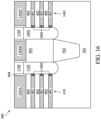
- FIGS. 13 , 14 , 15 , and 16 respectively illustrate cross-sectional views of the GAA transistor 300 , in various other embodiments.
- the cross-sectional views of FIGS. 13 - 16 are each cut in a direction along the lengthwise direction of a number of channel layers of the GAA transistor 300 (e.g., cross-section A-A indicated in FIG. 1 ).
- the semiconductor cladding layer 602 can further extend into the STI 502 and may contact the substrate 302 . As such, with a portion of the sidewall (of the semiconductor cladding layer 602 ) contacts the inactive metal gate structure 1202 B, a remaining portion of the sidewall can contact a sidewall of the STI 502 .
- the semiconductor cladding layer 602 may be formed following the formation of the STI 502 . For example, prior to forming the fin structure 410 , there may be one or more other stacks, each of which includes a single semiconductor layer 402 or multiple vertically spaced semiconductor layers 402 , formed over the substrate.
- Such other stacks may couple to the stack (later to form the fin structure 410 ), with a portion of the substrate 302 as a semiconductor interface.
- the semiconductor interface may become the semiconductor cladding layer 602 , as shown in FIG. 13 , e.g., extending from the substrate 302 .
- the GAA transistor 300 can further include a dummy gate structure 1402 , which can be a remaining portion of the dummy gate structure 802 B.
- the semiconductor cladding layer 602 can overlay a first portion of the top surface of the STI 502
- the dummy gate structure 1402 can overlay a second portion of the top surface of the STI 502 .
- respective top surfaces of the semiconductor cladding layer 602 and the dummy gate structure 1402 can level with each other, which causes the inactive gate structure 1202 B to be in contact with such a coplanar top surface, as shown in FIG. 14 .
- the semiconductor cladding layer 602 can have a non-planar top surface.
- such a non-planar top surface of the semiconductor cladding layer 602 can be formed during the etching process 701 (e.g., operation 210 of FIG. 2 ), or during the process of removing the dummy gate structure 802 B (e.g., FIG. 12 ).
- the non-planar top surface includes a curvature-based top surface that has a single arc, it should be understood that the non-planar top surface can have any number of arcs (e.g., some of which inwardly protrude and some of which outwardly protrude), while remaining within the scope of the present disclosure. Further, the non-planar top surface can have any number of valleys (e.g., an edge-based top surface), in some other embodiments.
- the GAA transistor 300 can further include another fin (or stack) structure of the semiconductor layers 402 (e.g., 1601 ) that is laterally spaced apart from the stack (or fin) structure 410 .
- the stack 1601 may mirror from the fin structure 410 with respect to the semiconductor cladding layer 602 .
- a source/drain structure 1602 is formed.
- Such a source/drain structure 1601 can be formed in similar techniques as the source/drain structure 1102 , e.g., through epitaxially growth along asymmetric sidewalls of a source/drain recess.
- the GAA transistor 300 can further include another active (e.g., metal) gate structure wrapping around each of the semiconductor layers 402 of the stack structure 1601 .
- a semiconductor device in one aspect of the present disclosure, includes a substrate.
- the semiconductor device includes a first plurality of channel layers disposed over the substrate, wherein the first plurality of channel layers all extend along a first direction and are vertically spaced from each other.
- the semiconductor device includes a first active gate structure that extends along a second direction perpendicular to the first direction and wraps around each of the first plurality of channel layers.
- the semiconductor device includes a first source/drain structure that includes a first sidewall and a second sidewall facing toward and away from the first direction, respectively.
- the semiconductor device includes a semiconductor cladding layer, integrally formed as a one-piece structure, that extends across the first plurality of channel layers.
- the first source/drain structure is coupled to each of the first plurality of channel layers through the first sidewall of the first source/drain structure and to the semiconductor cladding layer through the second sidewall of the first source/drain structure.
- a semiconductor device in another aspect of the present disclosure, includes an active gate structure extending along a first lateral direction.
- the semiconductor device includes an inactive gate structure also extending along the first lateral direction.
- the semiconductor device includes a first epitaxial structure disposed between the active gate structure and the inactive gate structure along a second lateral direction perpendicular to the first lateral direction.
- the active gate structure wraps around each of a plurality of channel layers that extend along the second direction, and the inactive gate structure straddles a semiconductor cladding layer that continuously extends along a first sidewall of the first epitaxial structure and across the plurality of channel layers.
- a method for making a semiconductor device includes forming a fin structure that extends along a first direction.
- the fin structure includes a plurality of channel layers and a plurality of sacrificial layers alternately stacked on top of one another.
- the method includes forming a semiconductor cladding layer that extends along a sidewall of the fin structure.
- the method includes etching a first portion of the fin structure, thereby exposing a sidewall of the semiconductor cladding layer.
- the method includes epitaxially growing a source/drain structure from the channel layers of a second portion of the fin structure and the semiconductor cladding layer.
Landscapes
- Insulated Gate Type Field-Effect Transistor (AREA)
Abstract
Description
HCl through HCn represent the respective thicknesses/heights of a number of semiconductor layers (which can each be the
HCIl through HCIn represent respective thicknesses/heights of a number of semiconductor layers (which can be the semiconductor cladding layer 602), and HSl through HSm represent respective thicknesses/heights of a number of non-semiconductor layers (which is absent in the illustrated example of
Claims (20)
Priority Applications (2)
| Application Number | Priority Date | Filing Date | Title |
|---|---|---|---|
| US17/461,536 US12176409B2 (en) | 2021-08-30 | 2021-08-30 | Semiconductor devices and methods of manufacturing thereof |
| US18/954,042 US20250081532A1 (en) | 2021-08-30 | 2024-11-20 | Semiconductor devices and methods of manufacturing thereof |
Applications Claiming Priority (1)
| Application Number | Priority Date | Filing Date | Title |
|---|---|---|---|
| US17/461,536 US12176409B2 (en) | 2021-08-30 | 2021-08-30 | Semiconductor devices and methods of manufacturing thereof |
Related Child Applications (1)
| Application Number | Title | Priority Date | Filing Date |
|---|---|---|---|
| US18/954,042 Division US20250081532A1 (en) | 2021-08-30 | 2024-11-20 | Semiconductor devices and methods of manufacturing thereof |
Publications (2)
| Publication Number | Publication Date |
|---|---|
| US20230068279A1 US20230068279A1 (en) | 2023-03-02 |
| US12176409B2 true US12176409B2 (en) | 2024-12-24 |
Family
ID=85287030
Family Applications (2)
| Application Number | Title | Priority Date | Filing Date |
|---|---|---|---|
| US17/461,536 Active 2043-03-08 US12176409B2 (en) | 2021-08-30 | 2021-08-30 | Semiconductor devices and methods of manufacturing thereof |
| US18/954,042 Pending US20250081532A1 (en) | 2021-08-30 | 2024-11-20 | Semiconductor devices and methods of manufacturing thereof |
Family Applications After (1)
| Application Number | Title | Priority Date | Filing Date |
|---|---|---|---|
| US18/954,042 Pending US20250081532A1 (en) | 2021-08-30 | 2024-11-20 | Semiconductor devices and methods of manufacturing thereof |
Country Status (1)
| Country | Link |
|---|---|
| US (2) | US12176409B2 (en) |
Citations (4)
| Publication number | Priority date | Publication date | Assignee | Title |
|---|---|---|---|---|
| US20230063087A1 (en) * | 2021-08-27 | 2023-03-02 | Taiwan Semiconductor Manufacturing Company, Ltd. | Semiconductor devices and methods of manufacturing thereof |
| US20230064705A1 (en) * | 2021-08-27 | 2023-03-02 | Taiwan Semiconductor Manufacturing Company, Ltd. | Semiconductor device structure and methods of forming the same |
| US20230067425A1 (en) * | 2021-08-28 | 2023-03-02 | Taiwan Semiconductor Manufacturing Company, Ltd. | Semiconductor devices and methods of manufacturing thereof |
| US12051737B2 (en) * | 2020-09-08 | 2024-07-30 | Semiconductor Manufacturing International (Shanghai) Corporation | Semiconductor device and fabrication method thereof |
-
2021
- 2021-08-30 US US17/461,536 patent/US12176409B2/en active Active
-
2024
- 2024-11-20 US US18/954,042 patent/US20250081532A1/en active Pending
Patent Citations (4)
| Publication number | Priority date | Publication date | Assignee | Title |
|---|---|---|---|---|
| US12051737B2 (en) * | 2020-09-08 | 2024-07-30 | Semiconductor Manufacturing International (Shanghai) Corporation | Semiconductor device and fabrication method thereof |
| US20230063087A1 (en) * | 2021-08-27 | 2023-03-02 | Taiwan Semiconductor Manufacturing Company, Ltd. | Semiconductor devices and methods of manufacturing thereof |
| US20230064705A1 (en) * | 2021-08-27 | 2023-03-02 | Taiwan Semiconductor Manufacturing Company, Ltd. | Semiconductor device structure and methods of forming the same |
| US20230067425A1 (en) * | 2021-08-28 | 2023-03-02 | Taiwan Semiconductor Manufacturing Company, Ltd. | Semiconductor devices and methods of manufacturing thereof |
Also Published As
| Publication number | Publication date |
|---|---|
| US20230068279A1 (en) | 2023-03-02 |
| US20250081532A1 (en) | 2025-03-06 |
Similar Documents
| Publication | Publication Date | Title |
|---|---|---|
| US12336271B2 (en) | Semiconductor devices and methods of manufacturing thereof | |
| US12261170B2 (en) | Semiconductor devices and methods of manufacturing thereof | |
| US12230545B2 (en) | Semiconductor devices including dummy gate dielectric layer and methods of manufacturing thereof | |
| US12402383B2 (en) | Semiconductor devices and methods of manufacturing thereof | |
| US20250120167A1 (en) | Semiconductor devices and methods of manufacturing thereof | |
| US12027521B2 (en) | Semiconductor devices and methods of manufacturing thereof | |
| US20260068252A1 (en) | Semiconductor devices and methods of manufacturing thereof | |
| US20250366061A1 (en) | Semiconductor devices and methods of manufacturing thereof | |
| US20250287647A1 (en) | Semiconductor devices and methods of manufacturing thereof | |
| US20240347615A1 (en) | Non-planar transistor devices and methods of manufacturing thereof | |
| US12176412B2 (en) | Semiconductor devices and methods of manufacturing thereof | |
| US12176409B2 (en) | Semiconductor devices and methods of manufacturing thereof | |
| US12094782B2 (en) | Semiconductor devices and methods of manufacturing thereof | |
| US20250081527A1 (en) | Semiconductor devices and methods of manufacturing thereof with diffusion cap layers |
Legal Events
| Date | Code | Title | Description |
|---|---|---|---|
| FEPP | Fee payment procedure |
Free format text: ENTITY STATUS SET TO UNDISCOUNTED (ORIGINAL EVENT CODE: BIG.); ENTITY STATUS OF PATENT OWNER: LARGE ENTITY |
|
| STPP | Information on status: patent application and granting procedure in general |
Free format text: DOCKETED NEW CASE - READY FOR EXAMINATION |
|
| AS | Assignment |
Owner name: TAIWAN SEMICONDUCTOR MANUFACTURING COMPANY, LTD., TAIWAN Free format text: ASSIGNMENT OF ASSIGNORS INTEREST;ASSIGNORS:LIN, SHIH-YAO;LEE, HSIAO WEN;CHANG, MING-CHING;SIGNING DATES FROM 20210307 TO 20210509;REEL/FRAME:060669/0015 |
|
| STPP | Information on status: patent application and granting procedure in general |
Free format text: NON FINAL ACTION MAILED |
|
| STPP | Information on status: patent application and granting procedure in general |
Free format text: RESPONSE TO NON-FINAL OFFICE ACTION ENTERED AND FORWARDED TO EXAMINER |
|
| STPP | Information on status: patent application and granting procedure in general |
Free format text: NOTICE OF ALLOWANCE MAILED -- APPLICATION RECEIVED IN OFFICE OF PUBLICATIONS |
|
| STPP | Information on status: patent application and granting procedure in general |
Free format text: PUBLICATIONS -- ISSUE FEE PAYMENT VERIFIED |
|
| STCF | Information on status: patent grant |
Free format text: PATENTED CASE |