US12174513B2 - Optical modulating device and optical apparatus employing the same - Google Patents
Optical modulating device and optical apparatus employing the same Download PDFInfo
- Publication number
- US12174513B2 US12174513B2 US17/101,200 US202017101200A US12174513B2 US 12174513 B2 US12174513 B2 US 12174513B2 US 202017101200 A US202017101200 A US 202017101200A US 12174513 B2 US12174513 B2 US 12174513B2
- Authority
- US
- United States
- Prior art keywords
- optical
- nano
- optical modulating
- antennas
- incidence
- Prior art date
- Legal status (The legal status is an assumption and is not a legal conclusion. Google has not performed a legal analysis and makes no representation as to the accuracy of the status listed.)
- Active, expires
Links
Images


Classifications
-
- G—PHYSICS
- G02—OPTICS
- G02F—OPTICAL DEVICES OR ARRANGEMENTS FOR THE CONTROL OF LIGHT BY MODIFICATION OF THE OPTICAL PROPERTIES OF THE MEDIA OF THE ELEMENTS INVOLVED THEREIN; NON-LINEAR OPTICS; FREQUENCY-CHANGING OF LIGHT; OPTICAL LOGIC ELEMENTS; OPTICAL ANALOGUE/DIGITAL CONVERTERS
- G02F1/00—Devices or arrangements for the control of the intensity, colour, phase, polarisation or direction of light arriving from an independent light source, e.g. switching, gating or modulating; Non-linear optics
- G02F1/29—Devices or arrangements for the control of the intensity, colour, phase, polarisation or direction of light arriving from an independent light source, e.g. switching, gating or modulating; Non-linear optics for the control of the position or the direction of light beams, i.e. deflection
- G02F1/292—Devices or arrangements for the control of the intensity, colour, phase, polarisation or direction of light arriving from an independent light source, e.g. switching, gating or modulating; Non-linear optics for the control of the position or the direction of light beams, i.e. deflection by controlled diffraction or phased-array beam steering
-
- G—PHYSICS
- G01—MEASURING; TESTING
- G01S—RADIO DIRECTION-FINDING; RADIO NAVIGATION; DETERMINING DISTANCE OR VELOCITY BY USE OF RADIO WAVES; LOCATING OR PRESENCE-DETECTING BY USE OF THE REFLECTION OR RERADIATION OF RADIO WAVES; ANALOGOUS ARRANGEMENTS USING OTHER WAVES
- G01S17/00—Systems using the reflection or reradiation of electromagnetic waves other than radio waves, e.g. lidar systems
- G01S17/88—Lidar systems specially adapted for specific applications
- G01S17/89—Lidar systems specially adapted for specific applications for mapping or imaging
-
- G—PHYSICS
- G01—MEASURING; TESTING
- G01S—RADIO DIRECTION-FINDING; RADIO NAVIGATION; DETERMINING DISTANCE OR VELOCITY BY USE OF RADIO WAVES; LOCATING OR PRESENCE-DETECTING BY USE OF THE REFLECTION OR RERADIATION OF RADIO WAVES; ANALOGOUS ARRANGEMENTS USING OTHER WAVES
- G01S7/00—Details of systems according to groups G01S13/00, G01S15/00, G01S17/00
- G01S7/48—Details of systems according to groups G01S13/00, G01S15/00, G01S17/00 of systems according to group G01S17/00
- G01S7/481—Constructional features, e.g. arrangements of optical elements
- G01S7/4814—Constructional features, e.g. arrangements of optical elements of transmitters alone
-
- G—PHYSICS
- G01—MEASURING; TESTING
- G01S—RADIO DIRECTION-FINDING; RADIO NAVIGATION; DETERMINING DISTANCE OR VELOCITY BY USE OF RADIO WAVES; LOCATING OR PRESENCE-DETECTING BY USE OF THE REFLECTION OR RERADIATION OF RADIO WAVES; ANALOGOUS ARRANGEMENTS USING OTHER WAVES
- G01S7/00—Details of systems according to groups G01S13/00, G01S15/00, G01S17/00
- G01S7/48—Details of systems according to groups G01S13/00, G01S15/00, G01S17/00 of systems according to group G01S17/00
- G01S7/481—Constructional features, e.g. arrangements of optical elements
- G01S7/4817—Constructional features, e.g. arrangements of optical elements relating to scanning
-
- G—PHYSICS
- G02—OPTICS
- G02B—OPTICAL ELEMENTS, SYSTEMS OR APPARATUS
- G02B26/00—Optical devices or arrangements for the control of light using movable or deformable optical elements
- G02B26/02—Optical devices or arrangements for the control of light using movable or deformable optical elements for controlling the intensity of light
-
- G—PHYSICS
- G02—OPTICS
- G02B—OPTICAL ELEMENTS, SYSTEMS OR APPARATUS
- G02B26/00—Optical devices or arrangements for the control of light using movable or deformable optical elements
- G02B26/06—Optical devices or arrangements for the control of light using movable or deformable optical elements for controlling the phase of light
-
- G—PHYSICS
- G02—OPTICS
- G02B—OPTICAL ELEMENTS, SYSTEMS OR APPARATUS
- G02B5/00—Optical elements other than lenses
- G02B5/008—Surface plasmon devices
-
- G—PHYSICS
- G02—OPTICS
- G02F—OPTICAL DEVICES OR ARRANGEMENTS FOR THE CONTROL OF LIGHT BY MODIFICATION OF THE OPTICAL PROPERTIES OF THE MEDIA OF THE ELEMENTS INVOLVED THEREIN; NON-LINEAR OPTICS; FREQUENCY-CHANGING OF LIGHT; OPTICAL LOGIC ELEMENTS; OPTICAL ANALOGUE/DIGITAL CONVERTERS
- G02F1/00—Devices or arrangements for the control of the intensity, colour, phase, polarisation or direction of light arriving from an independent light source, e.g. switching, gating or modulating; Non-linear optics
- G02F1/01—Devices or arrangements for the control of the intensity, colour, phase, polarisation or direction of light arriving from an independent light source, e.g. switching, gating or modulating; Non-linear optics for the control of the intensity, phase, polarisation or colour
- G02F1/0102—Constructional details, not otherwise provided for in this subclass
-
- G—PHYSICS
- G02—OPTICS
- G02F—OPTICAL DEVICES OR ARRANGEMENTS FOR THE CONTROL OF LIGHT BY MODIFICATION OF THE OPTICAL PROPERTIES OF THE MEDIA OF THE ELEMENTS INVOLVED THEREIN; NON-LINEAR OPTICS; FREQUENCY-CHANGING OF LIGHT; OPTICAL LOGIC ELEMENTS; OPTICAL ANALOGUE/DIGITAL CONVERTERS
- G02F1/00—Devices or arrangements for the control of the intensity, colour, phase, polarisation or direction of light arriving from an independent light source, e.g. switching, gating or modulating; Non-linear optics
- G02F1/29—Devices or arrangements for the control of the intensity, colour, phase, polarisation or direction of light arriving from an independent light source, e.g. switching, gating or modulating; Non-linear optics for the control of the position or the direction of light beams, i.e. deflection
-
- B—PERFORMING OPERATIONS; TRANSPORTING
- B82—NANOTECHNOLOGY
- B82Y—SPECIFIC USES OR APPLICATIONS OF NANOSTRUCTURES; MEASUREMENT OR ANALYSIS OF NANOSTRUCTURES; MANUFACTURE OR TREATMENT OF NANOSTRUCTURES
- B82Y20/00—Nanooptics, e.g. quantum optics or photonic crystals
-
- G—PHYSICS
- G02—OPTICS
- G02F—OPTICAL DEVICES OR ARRANGEMENTS FOR THE CONTROL OF LIGHT BY MODIFICATION OF THE OPTICAL PROPERTIES OF THE MEDIA OF THE ELEMENTS INVOLVED THEREIN; NON-LINEAR OPTICS; FREQUENCY-CHANGING OF LIGHT; OPTICAL LOGIC ELEMENTS; OPTICAL ANALOGUE/DIGITAL CONVERTERS
- G02F2202/00—Materials and properties
- G02F2202/20—LiNbO3, LiTaO3
-
- G—PHYSICS
- G02—OPTICS
- G02F—OPTICAL DEVICES OR ARRANGEMENTS FOR THE CONTROL OF LIGHT BY MODIFICATION OF THE OPTICAL PROPERTIES OF THE MEDIA OF THE ELEMENTS INVOLVED THEREIN; NON-LINEAR OPTICS; FREQUENCY-CHANGING OF LIGHT; OPTICAL LOGIC ELEMENTS; OPTICAL ANALOGUE/DIGITAL CONVERTERS
- G02F2202/00—Materials and properties
- G02F2202/30—Metamaterials
-
- G—PHYSICS
- G02—OPTICS
- G02F—OPTICAL DEVICES OR ARRANGEMENTS FOR THE CONTROL OF LIGHT BY MODIFICATION OF THE OPTICAL PROPERTIES OF THE MEDIA OF THE ELEMENTS INVOLVED THEREIN; NON-LINEAR OPTICS; FREQUENCY-CHANGING OF LIGHT; OPTICAL LOGIC ELEMENTS; OPTICAL ANALOGUE/DIGITAL CONVERTERS
- G02F2203/00—Function characteristic
- G02F2203/10—Function characteristic plasmon
-
- G—PHYSICS
- G02—OPTICS
- G02F—OPTICAL DEVICES OR ARRANGEMENTS FOR THE CONTROL OF LIGHT BY MODIFICATION OF THE OPTICAL PROPERTIES OF THE MEDIA OF THE ELEMENTS INVOLVED THEREIN; NON-LINEAR OPTICS; FREQUENCY-CHANGING OF LIGHT; OPTICAL LOGIC ELEMENTS; OPTICAL ANALOGUE/DIGITAL CONVERTERS
- G02F2203/00—Function characteristic
- G02F2203/24—Function characteristic beam steering
Definitions
- Example embodiments of the present disclosure relate to an optical modulating device and an optical apparatus employing the same.
- Optical modulating devices that change the transmission/reflection/scattering characteristics of light, phase, amplitude, polarization, intensity, and path are used in various optical apparatuses.
- optical modulating devices of various structures For example, a liquid crystal having optical anisotropy or a microelectromechanical system (MEMS) structure using micro-mechanical movement of light blocking/reflecting elements is used in general optical modulating devices.
- MEMS microelectromechanical system
- These optical modulating devices have a limit in response time due to the characteristics of a driving method. In the case of the MEMS structure, it is necessary to correct the nonlinearity of the voltage-displacement characteristic, and an optimized driving voltage profile to correct the influence of vibration of a motion system must be secured.
- One or more example embodiments provide an optical modulating device configured to reduce a side lobe.
- One or more example embodiments provide an optical modulating device configured to operate in high-speed and having a small dispersion of response.
- an optical modulating device including an incidence optical system, an optical modulating assembly including a plurality of nano-antennas that form a meta-grating based on a driving signal, the optical modulating assembly being configured to change a traveling direction of incidence light incident at an incidence angle from the incidence optical system based on an effective displacement of the meta-grating according to the driving signal, and an emission optical system configured to emit light steered by the optical modulating assembly, wherein the emission optical system is further configured to emit first-order diffraction light of the incidence light based on the meta-grating.
- a central axis of the emission optical system may be parallel to an optical axis of the first-order diffraction light when a displacement of the meta-grating is 0.
- a central axis of the emission optical system may coincide with an optical axis of the first-order diffraction light when a displacement of the meta-grating is 0.
- the incidence angle of the incidence light with respect to a surface normal vector of the optical modulating assembly is ⁇ in
- an angle of a central axis of the emission optical system is ⁇ out
- a wavelength of the incidence light is ⁇ 0
- a period of the meta-grating is ⁇
- the optical modulating assembly may further include a plurality of pixels, and the plurality of pixels respectively may include the plurality of nano-antennas.
- Each of the plurality of pixels may include one or more antenna groups, the one or more antenna groups may include the plurality of nano-antennas, and a period of the meta-grating may be equal to a period of the one or more antenna groups.
- Each of the plurality of pixels may include two or more antenna groups, and the driving signal of a same pattern may be applied to the two or more antenna groups included in a pixel among the plurality of pixels.
- a number of the plurality of pixels is L
- a number of antenna groups in each of the plurality of pixels is M
- a number of nano-antennas in each of the one or more antenna groups is N
- an n-th nano-antenna of an m-th antenna group of an I-th pixel MP is A lmn
- an optical intensity of A lmn is R lmn
- the plurality of pixels may be provided one-dimensionally.
- the plurality of pixels may be provided two-dimensionally.
- the optical modulating assembly may further include a reflector, and an active layer provided between the reflector and the plurality of nano-antennas, wherein optical properties of the active layer changes based on the driving signal.
- the plurality of nano-antennas may include metal antennas.
- the plurality of nano-antennas may include dielectric antennas.
- Each of the plurality of nano-antennas may have a Fabry-Perot resonance structure that includes a first reflection structure, a cavity layer provided on the first reflection structure, and a second reflection structure provided on the cavity layer.
- an optical modulating device including an incidence optical system, an optical modulating assembly including a plurality of pixels each including a plurality of nano-antennas, the optical modulating assembly being configured to change a traveling direction of incidence light incident at a fixed incidence angle from the incidence optical system by changing an optical intensity of the plurality of nano-antennas based on a periodic and discrete driving signal that is applied to the plurality of nano-antennas, an emission optical system configured to emit light steered by the optical modulating assembly, wherein, an incidence angle of the incidence light with respect to a surface normal vector of the optical modulating assembly is ⁇ in , an angle of a central axis of the emission optical system is ⁇ out , a wavelength of the incidence light is ⁇ 0 , and a period of a meta-grating is ⁇ , satisfies
- Each of the plurality of pixels may include one or more antenna groups, the one or more antenna groups respectively may include the plurality of nano-antennas, and a period of the driving signal may be equal to a period of the one or more antenna groups.
- the driving signal of a same pattern may be applied to two or more antenna groups in a pixel among the plurality of pixels.
- a number of the plurality of pixels is L
- a number of antenna groups in each of the plurality of pixels is M
- a number of nano-antennas in each of the one or more antenna groups is N
- an n-th nano-antenna of an m-th antenna group of an l-th pixel MP is A lmn
- an optical intensity of A lmn is R lmn , may satisfy
- an optical apparatus including an optical modulating device including an incidence optical system, an optical modulating assembly including a plurality of nano-antennas that form a meta-grating based on a driving signal, the optical modulating assembly being configured to change a traveling direction of incidence light incident at an incidence angle from the incidence optical system based on an effective displacement of the meta-grating according to the driving signal, and an emission optical system configured to emit light steered by the optical modulating assembly, wherein the emission optical system is further configured to emit first-order diffraction light of the incidence light based on the meta-grating.
- the optical apparatus may further include at least one of a light detection and ranging (LiDAR) device, a three-dimensional (3D) image obtaining device, a holographic display device, and a structured light generating device.
- LiDAR light detection and ranging
- 3D three-dimensional
- FIG. 1 is a diagram showing an optical modulating device according to an example embodiment
- FIGS. 2 A, 2 B, 2 C, and 2 D are diagrams showing an example of the displacement of a meta-grating when the optical intensity of a plurality of nano-antennas changes periodically and discretely;
- FIGS. 3 A, 3 B, and 3 C are diagrams showing a simulation environment for explaining a change in the geometric phase of first-order diffraction light due to a displacement of the meta-grating;
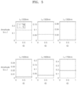
- FIG. 4 is a graph showing a simulation result by a simulation environment of FIGS. 3 A, 3 B, and 3 C , and shows a change in the geometric phase of first-order diffraction light according to a ratio of the displacement to the period;
- FIG. 5 is a graph showing a simulation result by a simulation environment of FIGS. 3 A, 3 B, and 3 C , and shows a change in the amplitude of first-order diffraction light according to a ratio of the displacement to the period;
- FIG. 6 is a cross-sectional view showing an optical modulating element according to an example embodiment
- FIG. 7 is a diagram showing examples of a planar shape of a nano-antenna according to an example embodiment
- FIGS. 8 A, 8 B, 8 C, 8 D, and 8 E are diagrams showing various nano-antenna having the Fabry-Perot resonance structure according to example embodiments;
- FIG. 9 is a configuration diagram showing an optical modulating element according to an example embodiment
- FIG. 10 is a diagram showing a result of simulating a reflectance spectrum of a nano-antenna of the optical modulating element shown in FIG. 9 according to an example embodiment
- FIG. 11 is a diagram showing a result of simulating a phase for each wavelength based on a discrete displacement of a meta-grating of the optical modulating element shown in FIG. 9 according to an example embodiment
- FIG. 12 is a diagram showing a result of simulating the intensity of first-order diffraction light with respect to incidence light based on the discrete displacement of a meta-grating of the optical modulating element shown in FIG. 9 according to an example embodiment
- FIGS. 13 and 14 are diagrams showing an optical modulating element according to example embodiments, wherein FIG. 13 shows an example where there is no relative phase difference between a plurality of pixels, and FIG. 14 shows an example where a beam is steered by a relative phase difference between the plurality of pixels;
- FIG. 15 is a diagram showing first-order diffraction light formed according to an example embodiment of the optical modulating element shown in FIG. 13 ;
- FIG. 16 is a diagram showing first-order diffraction light formed according to an example embodiment of the optical modulating element shown in FIG. 14 ;
- FIGS. 17 A and 17 B are diagrams of an example of a structure in which a plurality of pixels are two-dimensionally arranged in a Cartesian coordinate;
- FIGS. 18 A to 18 C are diagrams showing examples of various duty ratios of a meta-grating
- FIG. 19 is a conceptual diagram illustrating a beam steering device as an example of an optical modulating device according to an example embodiment
- FIG. 20 is a conceptual diagram illustrating a beam steering device as an example of an optical modulating device according to an example embodiment
- FIG. 21 is a block diagram of an example of an optical apparatus employing the optical modulating device according to an example embodiment.
- FIGS. 22 and 23 are conceptual diagrams illustrating an example where a light detection and ranging (LiDAR) device including an optical modulating device according to an example embodiment is applied to a vehicle, wherein FIG. 22 is a side view, and FIG. 23 is a plan view.
- LiDAR light detection and ranging
- the expression, “at least one of a, b, and c,” should be understood as including only a, only b, only c, both a and b, both a and c, both b and c, or all of a, b, and c.
- FIG. 1 is a diagram showing an optical modulating device 1 according to an example embodiment.
- FIGS. 2 A to 2 D are diagrams showing an example of the displacement of a meta-grating MG when the optical intensity of a plurality of nano-antennas NA changes periodically and discretely.
- the optical modulating device 1 of an example embodiment may include an incidence optical system 10 , an optical modulating element 20 that may include the plurality of nano-antennas NA that form the meta-grating MG or an effective grating by a driving signal and changes a traveling direction of incidence light L 1 incident at a fixed incidence angle ⁇ in from the incidence optical system 10 by using an effective displacement of the meta-grating MG according to the driving signal applied to the plurality of nano-antennas NA.
- the optical modulating device 1 may also include an emission optical system 30 through which light L 2 steered by the optical modulating element 20 is emitted.
- the emission optical system 30 may emit first-order diffraction light of the incidence light L 1 by the meta-grating MG.
- the optical modulating device 1 may further include a driving signal applier 40 that applies the driving signal to the plurality of nano-antennas NA.
- the incidence optical system 10 may include a light source.
- the incidence optical system 10 may include one or more optical elements, for example, a lens, which shapes light radiated from the light source into the incidence light L 1 of a desired shape.
- At least one of the length, width, thickness, and interval of the plurality of nano-antennas NA may be less than the wavelength of the incidence light L 1 .
- the optical intensity of each nano-antenna NA for example, the intensity of reflection/transmission/scattering, may be individually adjusted by applying the driving signal, for example, a voltage, to each nano-antenna NA. As a result, an effect similar to that of the meta-grating MG causing displacement may be obtained.
- a periodic displacement of the meta-grating MG may be induced by applying a periodic and discrete driving signal to the plurality of nano-antennas NA, and accordingly, a high-order diffraction component of light incident on the plurality of nano-antennas NA may have a geometric phase proportional to the displacement of the meta-grating MG.
- the optical modulating element 20 may include a plurality of pixels MP.
- Each of the plurality of pixels MP may include the plurality of nano-antennas NA.
- the periodic and discrete driving signal is applied to the plurality of nano-antennas NA of the plurality of pixels MP, the optical intensity of the plurality of nano-antennas NA changes, and the traveling direction of the incidence light L 1 from the incidence optical system 10 may change.
- a pattern of the driving signal may be periodic with respect to each pixel MP.
- Each of the plurality of pixels MP may include one or more antenna groups AG.
- Each antenna group AG may include the plurality of nano-antennas NA.
- the driving signal may be periodic with respect to each antenna group AG.
- the period of the pattern of the driving signal may be the same as the period of the antenna group AG.
- driving signals of the same pattern may be applied to the two or more antenna groups AG.
- the number of nano-antennas NA of each pixel MP may be appropriately determined according to the range and step of the geometric phase to be expressed. As the number of antenna groups AG of each pixel MP increases, the accuracy of beam steering may be improved. Therefore, it is ideal that the number of antenna groups AG of each pixel MP is infinite, but the number of antenna groups AG may be appropriately determined according to the required precision of beam steering. For example, each pixel MP may include 2 to 3 antenna groups AG.
- the plurality of pixels MP may have a one-dimensional (1D) arrangement structure. 1D beam steering is possible by appropriately arranging geometric phases of the plurality of pixels MP.
- the plurality of pixels MP may have a two-dimensional (2D) arrangement structure. 2D beam steering is possible by appropriately arranging the geometric phases of the plurality of pixels MP that are two-dimensionally arranged.
- the light may be a plane wave, a spherical wave, a Gaussian beam, etc.
- Reflection light may include a main lobe and a side lobe.
- SNR signal-to-noise ratio
- first-order diffraction light of the light reflected from the optical modulating element 20 is emitted.
- Specular reflection light L 3 is 0th-order diffraction light of the incidence light L 1 when the displacement of the geometric phase of the plurality of pixels MP is 0.
- a ratio of the side lobe is lower than that of the 0th-order diffraction light.
- the optical modulating device 1 of the example embodiment may include the emission optical system 30 that emits the first-order diffraction light of the incidence light L 1 by the meta-grating MG.
- the emission optical system 30 may include one or more optical elements, for example, a lens, for shaping and emitting the first-order diffraction light into a desired shape.
- a central axis 31 of the emission optical system 30 may be parallel to an optical axis of the first-order diffraction light L 4 when the displacement of the meta-grating MG is 0.
- the central axis 31 of the emission optical system 30 may coincide with the optical axis of the first-order diffraction light L 4 when the displacement of the meta-grating MG is 0.
- a wavelength of the incidence light L 1 is denoted by ⁇ 0
- a period of the meta-grating MG is denoted by ⁇
- the driving signal may be patterned, and the period of the meta-grating MG may be the same as the period of the driving signal pattern applied to the plurality of nano-antennas NA.
- the number of pixels MP is denoted by L (L is a positive integer)
- the number of antenna groups AG in each pixel MP is denoted by M (M is a positive integer)
- the number of nano-antennas NA in each antenna group AG is denoted by N (N is a positive integer).
- R lmn may be determined as in Equation (1) below.
- d 1, 2, . . . , N
- mod is a modulus operator
- (n ⁇ d) mod N is the remainder of (n ⁇ d) divided by N.
- Equation (2) Equation (2)
- Equation (3) an effective displacement x l of the l-th pixel MP is as shown in Equation (3) below.
- a phase ⁇ l of the l-th pixel MP is as shown in Equation (4) below.
- the nano-antenna NA is schematically shown.
- the nano-antenna NA of a dark pattern represents a case in which R lmn is 1 due to its strong optical intensity
- the nano-antenna NA of a bright pattern represents a case in which R lmn is 0 due to its weak optical intensity.
- the displacement of the period ⁇ is defined as 0 based on the fact that the left two nano-antennas NA have strong optical intensity and the right two nano-antennas NA have weak optical intensity among four nano-antennas NA inside the meta-grating MG.
- N a greater number of nano-antennas NA must be disposed in each pixel MP, and a greater number of wiring structures for applying the driving signal must be disposed, which increase the complexity of the system. Therefore, an appropriate N value according to the required phase range and number of phase steps may be selected.
- U i ( x,y,z ) Ae ik(x sin ⁇ i ⁇ z cos ⁇ i)
- the effective grating has the period ⁇ .
- the wavefunction by the effective grating is expressed by a Fourier series is shown below.
- C p denotes a p-th order Fourier coefficient and is given as shown in Equation (6).
- ⁇ p which is a p-th order diffraction efficiency is
- a value in a grating plane of the light wave transmitted or reflected by the meta-grating MG satisfies the below.
- ⁇ p denotes a diffraction angle and satisfies the below.
- Equation (7) A coefficient U 0,p of the p-th order diffraction component satisfies Equation (7) below.
- a p-th order diffraction component U′ 0,p is obtained when the meta-grating MG has a displacement by x l .
- a p-th order Fourier coefficient C′ p when the meta-grating MG has the displacement satisfies Equation (8) below.
- a grating function g(x) is a periodic function with the period ⁇
- Equation (9) satisfies Equation (1) shown below.
- c p ′ e i ⁇ ⁇ 2 ⁇ ⁇ ⁇ ⁇ px l ⁇ ⁇ c p
- Equation (7) the coefficient U′ 0,p of the p-th order diffraction component when the meta-grating MG has the displacement by d satisfies the below.
- ⁇ l 2 ⁇ ⁇ ⁇ x l ⁇
- Equation (4) is verified.
- FIGS. 3 A to 3 C are diagrams showing a simulation environment for explaining a change in the geometric phase of first-order diffraction light due to a displacement of the meta-grating MG.
- a refractive index of a medium M is 1.0.
- the refractive index of a grating G is 1.2 and a dielectric constant is 1.44.
- the grating G is a square grating having a width of 500 nm and a height of 1000 nm, and has a period of 1000 nm.
- a light wave having two polarizations of transverse magnetic (TM) and transverse electric (TE) is simulated.
- An incidence angle of the light wave with respect to a vector perpendicular to the grating G is 65 degrees.
- the wavelength is simulated on the total of 6 cases from 1200 nm to 1700 nm at 100 nm intervals.
- FIGS. 3 A to 3 C show cases where displacements are 0, ⁇ /3, and 2 ⁇ /3, respectively.
- FIG. 4 is a graph showing a simulation result by a simulation environment of FIGS. 3 A to 3 C , and shows a change in a geometric phase ⁇ of first-order diffraction light according to a ratio of the displacement to the period ⁇ .
- the vertical axis is the geometric phase ⁇ of the first-order diffraction light. Referring to FIG. 4 , it may be seen that the phase of the first-order diffraction light changes in proportion to the displacement in a wide wavelength band.
- the range of the phase that may be expressed in each pixel MP needs to be wide, and the amplitude needs to be uniform while changing the phase. This is because if the amplitude changes as the phase is adjusted, a generated light wave may have an unwanted side lobe in addition to a main lobe, and thus the SNR may be decreased.
- FIG. 5 is a graph showing a simulation result by a simulation environment of FIGS. 3 A to 3 C , and shows a change in the amplitude of first-order diffraction light according to a ratio of the displacement to the period ⁇ .
- the vertical axis is the amplitude of the first-order diffraction light.
- FIG. 5 show that the amplitude of the first-order diffraction light is constant even if the displacement changes in a wide wavelength band.
- the optical intensity of the plurality of nano-antennas NA has the same effect as having a periodic structure, such as the meta-grating MG or effective grating.
- a periodic structure such as the meta-grating MG or effective grating.
- the optical modulating device 1 capable of phase-only-modulation may be implemented.
- the optical modulating element 20 may have various structures.
- FIG. 6 is a cross-sectional view showing an example embodiment of the optical modulating element 20 .
- the optical modulating element 20 may include a reflector 211 and an active layer 212 disposed between the reflector 211 and the plurality of nano-antennas NA and of which optical properties change according to a driving signal.
- An insulating layer may be disposed between the reflector 211 and the active layer 212 and/or between the active layer 212 and the plurality of nano-antennas NA.
- the optical modulating element 20 according to the example embodiment shown in FIG. 6 may include a first insulating layer 213 disposed between the reflector 211 and the active layer 212 , and a second insulating layer 214 disposed between the active layer 212 and the plurality of nano-antennas NA.
- the reflector 211 may be a back reflector electrode disposed below the active layer 212 .
- the reflector 211 may reflect light and simultaneously perform the function of an electrode.
- the reflector 211 may be optically coupled to the nano-antenna NA, and may reflect light by an optical interaction between the nano-antenna NA and the reflector 211 .
- the reflector 211 may include a predetermined conductor such as metal.
- the reflector 211 may include at least one metal selected from the group consisting of copper (Cu), aluminum (Al), nickel (Ni), iron (Fe), cobalt (Co), zinc (Zn), titanium (Ti), ruthenium (Ru), rhodium (Rh), palladium (Pd), platinum (Pt), osmium (Os), iridium (Ir), silver (Ag), gold (Au), etc. and may include an alloy including at least one of these metals.
- the reflector 211 may include a thin film in which metal nanoparticles such as Ag and Au are dispersed, a carbon nanostructure such as graphene or carbon nanotube (CNT), a conductive polymer such as poly(3,4-ethylenedioxythiophene) (PEDOT), polypyrrole (PPy), poly(3-hexylthiophene) (P3HT), etc., or may include a conductive oxide, etc.
- metal nanoparticles such as Ag and Au are dispersed
- a carbon nanostructure such as graphene or carbon nanotube (CNT)
- a conductive polymer such as poly(3,4-ethylenedioxythiophene) (PEDOT), polypyrrole (PPy), poly(3-hexylthiophene) (P3HT), etc.
- PEDOT poly(3,4-ethylenedioxythiophene)
- PPy polypyrrole
- P3HT poly(3-hexylthiophene)
- the nano-antenna NA may convert incidence light including both visible and invisible electromagnetic waves of a specific wavelength or frequency into the form of localized surface plasmon resonance and capture the energy of the light and may be referred to as a nano-structured antenna for light.
- the nano-antenna NA may be a conductive pattern (e.g., a metal pattern).
- the conductive pattern may be in contact with a non-conductive layer (e.g., a dielectric layer). Plasmon resonance may occur on the interface between the conductive pattern and the non-conductive layer (e.g., the dielectric layer).
- the non-conductive layer (e.g., the dielectric layer) may be the second insulating layer 214 , or may be a layer separate from the second insulating layer 214 .
- the conductive pattern itself is regarded as a nano-antenna N 10 .
- an interface where surface plasmon resonance occurs may be collectively referred to as a “meta surface” or a “meta structure”.
- FIG. 7 is a diagram showing examples of a planar shape of the nano-antenna NA.
- the nano-antenna NA may have various planar shapes such as square, rectangular, circular, donut-shaped, and cross-shaped.
- the nano-antenna NA may have a dimension of a sub-wavelength.
- the sub-wavelength may be a dimension smaller than the operating wavelength of the nano-antenna NA.
- Any one dimension forming the shape of the nano-antenna NA, for example, at least one of the thickness, width, length, or interval between the nano-antennas NA may have the dimension of the sub-wavelength.
- the resonance wavelength may vary depending on the shape or dimension of the nano-antenna NA.
- the nano-antenna NA may include a metal material having high conductivity by which surface plasmon excitation may occur.
- the nano-antenna NA may include at least one metal selected from the group consisting of Cu, Al, Ni, Fe, Co, Zn, Ti, Ru, Rh, Pd, Pt, Os, Ir, Ag, Au, etc., and may include an alloy including at least one of these metals.
- the nano-antenna NA may include a thin film in which metal nanoparticles such as Ag and Au are dispersed, a carbon nanostructure such as graphene or CNT, a conductive polymer such as (PEDOT), polypyrrole (PPy), poly(3-hexylthiophene) (P3HT), etc., or may include a conductive oxide, etc.
- the nano-antenna NA and the reflector 211 may include different metals.
- the nano-antenna NA may be a dielectric antenna.
- the active layer 212 may be a layer of which physical properties change according to its electrical conditions.
- the permittivity or refractive index of the active layer 212 may change according to electrical conditions related to the active layer 212 and its surrounding region.
- a change in the dielectric constant of the active layer 212 may be due to a change in the charge concentration (charge density) of the region(s) in the active layer 212 .
- the permittivity of the active layer 212 may change by the charge concentration (charge density) of the region(s) in the active layer 212 .
- the permittivity of the active layer 212 may change according to an electric field or voltage applied to the active layer 212 .
- the active layer 212 may include, for example, a semiconductor, an oxide, a nitride, or a liquid crystal.
- the active layer 212 may include a transparent conductive oxide (TCO) such as indium tin oxide (ITO), indium zinc oxide (IZO), aluminum zinc oxide (AZO), gallium zinc oxide (GZO), aluminum gallium zinc oxide (AGZO), and gallium indium zinc oxide (GIZO).
- TCO transparent conductive oxide
- ITO indium tin oxide
- IZO indium zinc oxide
- AZO aluminum zinc oxide
- GZO gallium zinc oxide
- AGZO aluminum gallium zinc oxide
- GIZO gallium indium zinc oxide
- the active layer 212 may include a transition metal nitride (TMN) such as titanium nitride (TiN), zirconium nitride (ZrN), hafnium nitride (HfN), and tantalum nitride (TaN), a phase change material, graphene, a transition metal dichalcogenide, or a 2D material.
- TBN transition metal nitride
- TiN titanium nitride
- ZrN zirconium nitride
- hafnium nitride HfN
- tantalum nitride TaN
- phase change material graphene
- graphene graphene
- a transition metal dichalcogenide or a 2D material.
- EO electro-optic
- the EO material may include, for example, a crystalline material such as lithium niobium trioxide (LiNbO 3 ), lithium tantalum oxide (LiTaO 3 ), potassium tantalate niobate (KTN), or lead zirconate titanate (PZT), or may include various polymers having EO properties.
- a crystalline material such as lithium niobium trioxide (LiNbO 3 ), lithium tantalum oxide (LiTaO 3 ), potassium tantalate niobate (KTN), or lead zirconate titanate (PZT)
- LiNbO 3 lithium niobium trioxide
- LiTaO 3 lithium tantalum oxide
- KTN potassium tantalate niobate
- PZT lead zirconate titanate
- the first insulating layer 213 and the second insulating layer 214 may include an insulating material (a dielectric material). At least one of the first and second insulating layers 213 and 214 may include at least one of an insulating silicon compound and an insulating metal compound.
- the insulating silicon compound may include, for example, silicon oxide (SiOx), silicon nitride (SixNy), silicon oxynitride (SiON), etc.
- the insulating metal compound may include, for example, aluminum oxide (Al 2 O 3 ), hafnium oxide (HfO), zirconium oxide (ZrO), hafnium silicon oxide (HfSiO), etc.
- the first insulating layer 213 and the second insulating layer 214 may include the same material or may have different material configurations.
- the active layer 212 may be electrically insulated from the reflector 211 by the first insulating layer 213 , and the active layer 212 may be electrically insulated from the nano-antenna NA by the second insulating layer 214 .
- a voltage (a driving signal) applied between the reflector 211 and the active layer 212 the charge concentration in a first boundary region of the active layer 212 with the first insulating layer 213 may change.
- a voltage (a driving signal) applied between the active layer 212 and the nano-antenna NA the charge concentration in a second boundary region of the active layer 212 with the second insulating layer 214 may change.
- Each of the first boundary region and the second boundary region may be divided into a plurality of unit regions corresponding to the plurality of nano-antennas NA, and may be a charge accumulation region or a charge depletion region according to the voltage.
- the charge accumulation region may be formed in an upper portion of the active layer 212 .
- the charge depletion region may be formed in the upper portion of the active layer 212 .
- the charge accumulation region may be formed in a lower portion of the active layer 212 .
- the charge depletion region may be formed in the lower portion of the active layer 212 .
- the reflection characteristic of the optical modulating element 20 may be controlled. Accordingly, the above-described meta-grating MG may be formed, and the direction of the first-order diffraction light may be controlled by appropriately arranging the geometric phases of the plurality of pixels MP to steer a beam.
- the optical modulating element 20 may be implemented by the plurality of nano-antennas NA having a Fabry-Perot resonance structure.
- FIGS. 8 A to 8 E are diagrams showing various example embodiments of the nano-antenna NA having the Fabry-Perot resonance structure.
- the nano-antenna NA may include a first reflection structure 221 , a cavity layer 222 provided on the first reflection structure 221 , and a second reflection structure 223 provided on the cavity layer 222 .
- both the first reflective structure 221 and the second reflective structure 223 may be distributed Bragg reflectors (DBRs) in which materials having different refractive indices are alternately stacked.
- DBRs distributed Bragg reflectors
- the first reflection structure 221 may be the DBR
- the second reflection structure 223 may be a high contrast grating (HCG) in which a column, a disk, a grating structure, etc. with a high refractive index are surrounded by a medium with a low refractive index.
- HCG high contrast grating
- the first reflective structure 221 may be the HCG
- the second reflective structure 223 may be the DBR.
- both the first reflective structure 221 and the second reflective structure 223 may be HCGs.
- One of the first reflective structure 221 , the cavity layer 222 , and the second reflective structure 223 may be an active layer of which optical properties such as a refractive index and a dielectric constant are changed by a driving signal.
- the driving signal may be, for example, a voltage signal, and may be a heating signal that applies heat to a corresponding component.
- the cavity layer 222 may be an active layer.
- the cavity layer 222 may include the same material as the above-described active layer 212 in FIG. 6 .
- At least one of layers constituting the first reflective structure 221 or the second reflective structure 223 may be an active layer of which optical properties are changed by the driving signal.
- At least one layer of the first reflective structure 221 may be an EO material layer including an EO material of which effective permittivity changes when an electrical signal is applied. Accordingly, when power is applied from an external power source, the refractive index of the EO material layer of the first reflective structure 221 changes, and the phase of light resonating between the first reflective structure 221 and the second reflective structure 223 changes.
- a resonance wavelength, a resonance wavelength width, a resonance polarization characteristic, a resonance angle, reflection/transmission/scattering characteristics, etc. may vary.
- the optical modulating element 20 having characteristics suitable for the purpose may be manufactured by controlling the structure/shape and arrangement method of the nano-antenna NA.
- An apparatus for steering a beam in a predetermined direction may be implemented by using the optical modulating element 20 according to example embodiments.
- FIG. 9 is a configuration diagram showing an example embodiment of the optical modulating element 20 .
- the optical modulating element 20 shown in FIG. 9 has a structure shown in FIG. 6 , the lower reflector 211 includes Au, the active layer 212 includes ITO, the first insulating layer 214 includes oxide, and the nano-antenna NA includes Au.
- the thickness of the active layer 212 may be 10 nm, and the thickness of the lower reflector 211 may be semi-infinite.
- a driving signal is applied between the active layer 212 and the nano-antenna NA.
- the active layer 212 is a common electrode, and an individual driving signal is applied to the nano-antenna NA.
- the nano-antenna NA has a period of 400 nm, a width of 200 nm, and a thickness of 20 nm.
- the pixel MP has a period of 2400 nm.
- FIG. 10 is a diagram showing a result of simulating a reflectance spectrum of the nano-antenna NA according to an example embodiment of the optical modulating element 20 shown in FIG. 9 .
- 0 V is applied to the active layer 212 and a positive voltage Va is applied to the nano-antenna NA
- the concentration of free electrons increases in a boundary region between the active layer 212 and the second insulating layer 214 , resulting in a charge accumulation state ACC in FIG. 9 .
- reflectance is blue-shifted as indicated by BS in FIG. 10 .
- the concentration of free electrons decreases in the boundary region between the active layer 212 and the second insulating layer 214 , resulting in a charge depletion state DEP in FIG. 9 .
- the reflectance is red-shifted as indicated by RS in FIG. 10 .
- the reflectance of the nano-antenna NA is 38% in the charge accumulation state and is 22% in the charge depletion state. That is, a contrast of 16% p(percent point), which is a difference in the reflectance, may be obtained.
- FIG. 11 is a diagram showing a result of simulating the phase ⁇ for each wavelength based on a discrete displacement of the meta-grating MG according to an example embodiment of the optical modulating element 20 shown in FIG. 9 .
- the driving signals applied to the six nano-antennas NA discretely change as shown below.
- V a denotes a voltage forming a charge accumulation region
- V d denotes a voltage forming a charge depletion region.
- the geometric phase ⁇ has values of 0 degrees, 60 degrees, 120 degrees, 180 degrees, 240 degrees, and 360 degrees according to the displacement.
- the values of the geometric phase ⁇ commonly appears in a wavelength of 1000 nm to 180 nm.
- FIG. 12 is a diagram showing a result of simulating the intensity of first-order diffraction light with respect to incidence light based on the discrete displacement of the meta-grating MG according to an example embodiment of the optical modulating element 20 shown in FIG. 9 .
- FIG. 12 shows a ratio (%) of the intensity of the first-order diffraction light to the intensity of the incidence light for each wavelength as the displacement of the meta-grating MG discretely increases.
- FIG. 12 shows efficiency of about 5% at about 1500 nm. There is an advantage that the efficiency does not change when the displacement changes for a fixed wavelength. An efficiency value may vary depending on the wavelength because contrast in the reflectance of the nano-antenna NA constituting the meta-grating MG is the same as the contrast shown in FIG. 10 .
- FIGS. 13 and 14 are schematic diagrams showing an example embodiment of the optical modulating element 20 .
- FIG. 13 shows an example where there is no relative phase difference between the plurality of pixels MP.
- FIG. 14 shows an example where a beam is steered by a relative phase difference between the plurality of pixels MP.
- the optical modulating element 20 shown in FIGS. 13 and 14 has a structure shown in FIG. 6 , the lower reflector 211 includes Au, the active layer 212 includes ITO, the first insulating layer 214 includes oxide, and the nano-antenna NA includes Au.
- the active layer 212 has a thickness of 5 nm and a doping concentration of 5 ⁇ 10 20 /cm 3 .
- the second insulating layer 214 has a thickness of 10 nm and a refractive index of 2.0.
- the thickness of the lower reflector 211 is semi-infinite.
- a driving signal is applied between the active layer 212 and the nano-antenna NA.
- the active layer 212 is a common electrode, and an individual driving signal is applied to the nano-antenna NA.
- the nano-antenna NA has a length of 210 nm, a thickness of 50 nm, and a period of 330 nm.
- a driving signal V lmn applied to an arbitrary nano-antenna A lmn has a relationship that satisfies the following conditional equation below.
- V lmn ⁇ V a if ⁇ n ⁇ 2 V d otherwise
- driving signal patterns of the pixels MP 1 and MP 2 are the same and are as follows.
- the geometric phase according to the displacement of the meta-grating MG is the same in the pixels MP 1 and MP 2 .
- An emission angle of first-order diffraction light may be calculated by the equation shown below.
- ⁇ out sin - 1 ( sin ⁇ ⁇ in - ⁇ 0 ⁇ )
- A denotes the period of the driving signal pattern, that is, the period of the antenna group AG, and is 1320 nm.
- A denotes the period of the driving signal pattern, that is, the period of the antenna group AG, and is 1320 nm.
- the emission angle of the first-order diffraction light is ⁇ 17.8 degrees.
- FIG. 15 is a diagram showing first-order diffraction light formed according to an example embodiment of the optical modulating element 20 shown in FIG. 13 . As shown in FIG. 15 , it may be seen that the first-order diffraction light having a very small side lobe is formed at an emission angle of about ⁇ 17.8 degrees.
- the pixels MP 1 and MP 2 have a geometric phase difference of 180 degrees.
- the driving signal V lmn applied to the arbitrary nano-antenna A lmn has a relationship that satisfies the following conditional equation shown below.
- V lmn ⁇ V a if ⁇ ( 2 ⁇ l + n + 1 ) ⁇ mod ⁇ 4 ⁇ 1 V d otherwise
- the driving signal patterns of the pixels MP 1 and MP 2 are as follows.
- the geometric phase of the pixel MP 1 is 0 degrees
- the geometric phase of the pixel MP 2 is 180 degrees
- the two pixels MP 1 and MP 2 having 0 degrees and 180 degrees respectively form a super-pixel.
- a period ⁇ sp of the super pixel is twice the period of each of the pixels MP 1 and MP 2
- the two antenna groups AG 1 and AG 2 are included in each of the pixels MP 1 and MP 2
- the period ⁇ sp of the super pixel is 4 times the period ⁇ of the antenna groups AG 1 and AG 2 .
- An emission angle of first-order diffraction light may be calculated by the equation shown below.
- ⁇ out sin - 1 ( sin ⁇ ⁇ in - ⁇ 0 ⁇ + ⁇ 0 ⁇ SP ) .
- FIG. 16 is a diagram showing first-order diffraction light formed according to an example embodiment of the optical modulating element 20 shown in FIG. 14 . As shown in FIG. 16 , it may be seen that first-order diffraction light having a very small side lobe is formed at an emission angle of about ⁇ 0.84 degrees.
- the plurality of pixels MP may be two-dimensionally arranged.
- FIGS. 17 A and 17 B are diagrams showing an example of a structure in which the plurality of pixels MP are two-dimensionally arranged in a Cartesian coordinate.
- FIG. 17 A shows a 2D arrangement of the plurality of pixels MP.
- FIG. 17 B shows the phase ⁇ of the meta-grating MG corresponding to each of the plurality of pixels MP.
- each pixel MP includes two antenna groups AG, and each antenna group AG includes four nano-antennas NA.
- a periodic and discrete driving signal is applied to the plurality of nano-antennas NA of each pixel MP, an effective grating is formed in each pixel MP.
- the nano-antenna NA indicated by a dark pattern has a strong optical intensity
- the nano-antenna NA indicated by a bright pattern has a weak optical intensity.
- the incidence light L 1 may be incident on the plurality of pixels MP at the incidence angle of ⁇ with respect to a normal line Ln within a incidence plane S 1 perpendicular to the plurality of pixels MP.
- the first-order diffraction light is emitted in the direction of the normal line Ln.
- 2D beam steering is possible. Accordingly, when the phases of the meta-grating MG of the plurality of pixels MP are properly arranged, the 2D steered first-order diffraction light L 2 that is emitted along an emission plane S 2 having an angle with respect to the incidence plane S 1 may be obtained.
- driving signals are applied such that the meta-gratings MG of the four pixels MP in each row have geometric phase differences of 0 degrees, 90 degrees, 180 degrees, and 360 degrees, respectively, and that the meta-gratings MG of the four pixels MP in each column have geometric phase differences of 0 degrees, 90 degrees, 180 degrees, and 360 degrees, respectively.
- the driving signal is applied such that each pixel MP has a phase difference of 90 degrees from the neighboring pixel MP.
- 2D beam steering is possible.
- FIGS. 17 A and 17 B show the plurality of pixels MP having a 2D arrangement structure in the Cartesian coordinate but the plurality of pixels MP may be arranged in various coordinates such as a polar coordinate, a hexagonal coordinate, etc.
- the pattern of the driving signal may have various duty ratios. As a result, an effective grating having various duty ratios may be formed.
- the duty ratio of the meta-grating MG is 50%.
- Various duty ratios may be implemented by generalizing Equation (11) as shown below.
- C denotes a criterion which is N/2 in Equation (11).
- the generalized C may have a value of 1 to N ⁇ 1.
- FIGS. 18 A to 18 C are diagrams showing examples of various duty ratios of the meta-grating MG.
- the duty ratio of the meta-grating MG is 25%.
- the duty ratio of the meta-grating MG is 75%.
- the duty ratio may be appropriately determined in order to increase the ratio of light emitted in a desired direction and decrease the ratio of light emitted in an undesired direction.
- the effective grating or the meta-grating MG is formed by individually adjusting the optical intensity of the nano-antenna NA, that is, the intensity of transmission/reflection/scattering, and a high-order diffraction component of the incidence light wave has the geometric phase proportional to a displacement by causing the displacement in the optical intensity distribution of the nano-antenna NA inside the pixel MP.
- the optical modulating device 1 described above may more easily adjust the displacement of the meta-grating MG by digitizing and changing the optical intensity distribution of the nano-antenna NA. Therefore, a beam may be steered at various desired angles by using the digitalized control method.
- the amplitude of emission light is maintained constant within a steering range by steering the first-order diffraction light. Therefore, excellent steering light with a small ratio of the side lobe may be obtained.
- a wiring structure for applying a driving signal to the plurality of nano-antennas NA may be simple and a linear voltage-phase response characteristic may be obtained.
- the optical modulating device 1 operates in an all-solid-state where no mechanical movement exists, and thus a high-speed operation is possible, and the dispersion of response due to errors in the manufacturing process is small, and thus a uniform response characteristic may be obtained.
- FIG. 19 is a conceptual diagram illustrating a beam steering device 1000 A as an example of the optical modulating device 1 according to an example embodiment.
- a beam may be steered in a 1D direction by using the beam steering device 1000 A.
- the beam may be steered toward a predetermined object OBJ in a first direction D 1 .
- the beam steering device 1000 A may employ the optical modulating element 20 including the plurality of pixels MP that are one-dimensionally arranged.
- FIG. 20 is a conceptual diagram illustrating a beam steering device 1000 B as an example of the optical modulating device 1 according to an example embodiment.
- a beam may be steered in a 2D direction by using the beam steering device 1000 B.
- the beam may be steered toward the predetermined object OBJ in the first direction D 1 and a second direction D 2 perpendicular to the first direction D 1 .
- the beam steering device 1000 B may employ the optical modulating element 20 including the plurality of pixels MP that are two-dimensionally arranged.
- the beam steering devices 1000 A and 1000 B described with reference to FIGS. 19 and 20 may be non-mechanical ultrafast beam scanning apparatuses.
- FIG. 21 is a block diagram of an example of an optical apparatus 2 employing the optical modulating device 1 according to an example embodiment.
- the optical apparatus 2 may include a beam steering unit 1000 .
- the beam steering unit 1000 may include the optical modulating device 1 described according to example embodiments.
- the optical apparatus 2 may include a detection unit 2000 for detecting light that is steered by the beam steering unit 1000 and reflected by an object.
- the detection unit 2000 may include a plurality of light detection elements, and may further include other optical members.
- the optical apparatus 2 may further include a circuit unit 3000 connected to at least one of the beam steering unit 1000 and the detection unit 2000 .
- the circuit unit 3000 may include an operation unit that obtains and calculates data, and may further include a driving unit and a control unit. In addition, the circuit unit 3000 may further include a power supply unit and a memory.
- the beam steering unit 1000 of the example embodiment employing the optical modulating device 1 steers first-order diffraction light having a reduced side lobe, and thus the SNR of the detection unit 2000 may be improved.
- the beam steering unit 1000 has no mechanical movement for beam steering, and thus a high-speed operation is possible and a dispersion of response is small. Therefore, precise high-speed detection of light is possible.
- the optical apparatus 2 includes the beam steering unit 1000 and the detection unit 2000 in one device, but the beam steering unit 1000 and the detection unit 2000 may not be provided as a single device and may be separately provided in separate devices.
- the circuit unit 3000 is not connected to the beam steering unit 1000 or the detection unit 2000 by wire, but may be connected through wireless communication.
- the configuration of FIG. 21 may be variously modified.
- the optical modulating device 1 may be applied to various optical apparatuses.
- the optical modulating device 1 may be applied to a light detection and ranging (LiDAR) device.
- the LiDAR device may be a phase-shift device or a time-of-flight (TOF) device.
- the LiDAR device may be applied to autonomous vehicles, flying objects such as drones, mobile devices, small walking means (e.g., bicycles, motorcycles, strollers, boards, etc.), robots, human/animal assistance means (e.g., cane, helmet, jewelry, clothing, watches, bags, etc.), Internet of Things (IoT) devices/systems, security devices/systems, etc.
- IoT Internet of Things
- FIGS. 22 and 23 are conceptual diagrams illustrating a case where a LiDAR device 51 including the optical modulating device 1 according to an example embodiment is applied to a vehicle 50 .
- FIG. 22 is a side view of the vehicle 50
- FIG. 23 is a plan view of the vehicle 50 .
- the LiDAR device 51 may be applied to the vehicle 50 , and may be used to obtain information about an object 60 .
- the vehicle 50 may have an autonomous driving function.
- the LiDAR device 51 may be used to detect an object or person, that is, the object 60 , in the direction in which the vehicle 50 travels. Further, a distance to the object 60 may be measured using information such as a time difference between a transmission signal and a detection signal.
- the information about a nearby object 61 and a distant object 62 within the scan range may be obtained.
- the optical modulating device may be applied to various optical apparatuses other than the LiDAR device.
- various optical apparatuses other than the LiDAR device.
- three-dimensional (3D) information of a space and an object may be obtained through scanning, and thus the optical modulating device may be applied to a 3D image obtaining device or a 3D camera.
- the optical modulating device may be applied to a holographic display device and a structured light generating device.
- the optical modulating device may be applied to various optical apparatuses such as various beam scanning devices, hologram generating devices, optical coupling devices, variable focus lenses, depth sensors, etc.
- the optical modulating device may be applied to various fields in which a “meta surface” or a “meta structure” is used.
- the optical modulating device and the optical apparatus including the same according to the example embodiment may be applied to various optical and electronic device fields for various purposes.
- an optical modulating device capable of reducing a side lobe may be implemented.
- an optical modulating device capable of high-speed operation and a small dispersion of response may be implemented.
- first-order diffraction light is steered, and thus improved steering light with a small ratio of the side lobe may be obtained.
- the optical modulating device operates in an all-solid-state where no mechanical movement exists, and thus a high-speed operation is possible, and the dispersion of response due to errors in the manufacturing process is small, and thus a uniform response characteristic may be obtained.
Landscapes
- Physics & Mathematics (AREA)
- General Physics & Mathematics (AREA)
- Engineering & Computer Science (AREA)
- Optics & Photonics (AREA)
- Nonlinear Science (AREA)
- Computer Networks & Wireless Communication (AREA)
- Radar, Positioning & Navigation (AREA)
- Remote Sensing (AREA)
- Electromagnetism (AREA)
- Optical Modulation, Optical Deflection, Nonlinear Optics, Optical Demodulation, Optical Logic Elements (AREA)
Abstract
Description
where d=1, 2, . . . , N, and C is any one of 1 to N−1.
where d=1, 2, . . . , N, and C is any one of 1 to N−1.
R lm
U i(x,y,z)=Ae ik(x sin θ
U i(x,y,z=0)=Ae ikx sin
When Equations (7) and (10) are substituted to Equation (8), the below is satisfied.
are added as shown below.
-
- d=1, (V1, V2, V3, V4, V5, V6)=(Va, Va, Va, Vd, Vd, Vd)
- d=2, (V1, V2, V3, V4, V5, V6)=(Vd, Va, Va, Va, Vd, Vd)
- d=3, (V1, V2, V3, V4, V5, V6)=(Vd, Vd, Va, Va, Va, Vd)
- d=4, (V1, V2, V3, V4, V5, V6)=(Vd, Vd, Vd, Va, Va, Va)
- d=5, (V1, V2, V3, V4, V5, V6)=(Va, Vd, Vd, Vd, Va, Va)
- d=6, (V1, V2, V3, V4, V5, V6)=(Va, Va, Vd, Vd, Vd, Va)
-
- (V111, V112, V113, V114)=(Va, Va, Vd, Vd)
- (V121, V122, V123, V124)=(Va, Va, Vd, Vd)
- (V211, V212, V213, V214)=(Va, Va, Vd, Vd)
- (V221, V222, V223, V224)=(Va, Va, Vd, Vd)
-
- (V111, V112, V113, V114)=(Va, Va, Vd, Vd)
- (V121, V122, V123, V124)=(Va, Va, Vd, Vd)
- (V211, V212, V213, V214)=(Vd, Vd, Va, Va)
- (V221, V222, V223, V224)=(Vd, Vd, Va, Va)
Claims (18)
Applications Claiming Priority (2)
| Application Number | Priority Date | Filing Date | Title |
|---|---|---|---|
| KR10-2020-0080500 | 2020-06-30 | ||
| KR1020200080500A KR20220002791A (en) | 2020-06-30 | 2020-06-30 | Optical modulating device and apparatus using the same |
Publications (2)
| Publication Number | Publication Date |
|---|---|
| US20210405500A1 US20210405500A1 (en) | 2021-12-30 |
| US12174513B2 true US12174513B2 (en) | 2024-12-24 |
Family
ID=79032584
Family Applications (1)
| Application Number | Title | Priority Date | Filing Date |
|---|---|---|---|
| US17/101,200 Active 2043-10-26 US12174513B2 (en) | 2020-06-30 | 2020-11-23 | Optical modulating device and optical apparatus employing the same |
Country Status (2)
| Country | Link |
|---|---|
| US (1) | US12174513B2 (en) |
| KR (1) | KR20220002791A (en) |
Families Citing this family (5)
| Publication number | Priority date | Publication date | Assignee | Title |
|---|---|---|---|---|
| JP7616638B2 (en) * | 2020-12-01 | 2025-01-17 | 株式会社トプコン | Optical Scanning Device |
| US20230221416A1 (en) * | 2022-01-07 | 2023-07-13 | Samsung Electronics Co., Ltd. | Distance information acquisition apparatus and electronic apparatus including the same |
| CN118872152A (en) * | 2022-01-27 | 2024-10-29 | 华为技术有限公司 | Image sensor and electronic device |
| JP2023140757A (en) * | 2022-03-23 | 2023-10-05 | スタンレー電気株式会社 | Wavelength conversion device and lighting device |
| KR102741014B1 (en) * | 2022-10-05 | 2024-12-11 | 한국전자통신연구원 | meta-structure |
Citations (18)
| Publication number | Priority date | Publication date | Assignee | Title |
|---|---|---|---|---|
| US5222071A (en) | 1991-02-21 | 1993-06-22 | Board Of Trustees Leland Stanford, Jr. University | Dynamic optical grating device |
| US20020191913A1 (en) * | 2001-06-08 | 2002-12-19 | Honeywell International Inc. | Apparatus and method for processing light |
| US20100253995A1 (en) | 2007-10-19 | 2010-10-07 | Stephan Reichelt | Complex-Valued Spatial Light Modulator |
| US20140224989A1 (en) * | 2013-02-14 | 2014-08-14 | The Government Of The United States Of America, As Represented By The Secretary Of The Navy | Actively Tunable Polar-Dielectric Optical Devices |
| US20160170237A1 (en) * | 2010-12-30 | 2016-06-16 | Samsung Electronics Co., Ltd. | Light modulators and optical apparatuses including the same |
| US20160223723A1 (en) * | 2015-02-03 | 2016-08-04 | Samsung Electronics Co., Ltd. | Optical modulating device having gate structure |
| KR20180002212A (en) | 2016-06-29 | 2018-01-08 | 엘지이노텍 주식회사 | Semiconductor device module |
| US20180024412A1 (en) * | 2016-07-21 | 2018-01-25 | Samsung Electronics Co.,Ltd. | Beam steering device including p-n junction layer |
| US20180136537A1 (en) * | 2016-11-16 | 2018-05-17 | Samsung Electronics Co., Ltd. | Two-dimensional light modulating device and electronic apparatus including the same |
| US20180196137A1 (en) * | 2017-01-10 | 2018-07-12 | Samsung Electronics Co., Ltd. | Optical modulating device and system employing same |
| US20190025509A1 (en) | 2017-07-24 | 2019-01-24 | Samsung Electronics Co., Ltd. | Beam steering device and system including the same |
| US20190075275A1 (en) * | 2017-09-05 | 2019-03-07 | Samsung Electronics Co., Ltd. | Light modulating device and electronic apparatus including the same |
| US20190204492A1 (en) | 2018-01-03 | 2019-07-04 | Samsung Electronics Co., Ltd. | Active phase modulator and beam steering device |
| US20190265557A1 (en) * | 2017-09-28 | 2019-08-29 | Boe Technology Group Co., Ltd. | Liquid crystal grating and driving method thereof, display device |
| US20190294019A1 (en) * | 2018-03-23 | 2019-09-26 | Samsung Electronics Co., Ltd. | Beam scanning apparatus and optical apparatus including the same |
| KR20190136434A (en) | 2018-05-30 | 2019-12-10 | 삼성전자주식회사 | Optical modulating device and apparatus including the same |
| US20210157179A1 (en) * | 2019-11-25 | 2021-05-27 | Huawei Technologies Canada Co., Ltd. | Apparatus for plasmonic nanoantenna optical beam phase-shifter and steerer |
| US20220252945A1 (en) * | 2019-06-24 | 2022-08-11 | Agency For Science, Technology And Research | Spatial light modulator and method of forming the same |
-
2020
- 2020-06-30 KR KR1020200080500A patent/KR20220002791A/en active Pending
- 2020-11-23 US US17/101,200 patent/US12174513B2/en active Active
Patent Citations (21)
| Publication number | Priority date | Publication date | Assignee | Title |
|---|---|---|---|---|
| US5222071A (en) | 1991-02-21 | 1993-06-22 | Board Of Trustees Leland Stanford, Jr. University | Dynamic optical grating device |
| US20020191913A1 (en) * | 2001-06-08 | 2002-12-19 | Honeywell International Inc. | Apparatus and method for processing light |
| US20100253995A1 (en) | 2007-10-19 | 2010-10-07 | Stephan Reichelt | Complex-Valued Spatial Light Modulator |
| US20160170237A1 (en) * | 2010-12-30 | 2016-06-16 | Samsung Electronics Co., Ltd. | Light modulators and optical apparatuses including the same |
| US20140224989A1 (en) * | 2013-02-14 | 2014-08-14 | The Government Of The United States Of America, As Represented By The Secretary Of The Navy | Actively Tunable Polar-Dielectric Optical Devices |
| US20160223723A1 (en) * | 2015-02-03 | 2016-08-04 | Samsung Electronics Co., Ltd. | Optical modulating device having gate structure |
| KR20180002212A (en) | 2016-06-29 | 2018-01-08 | 엘지이노텍 주식회사 | Semiconductor device module |
| US20180024412A1 (en) * | 2016-07-21 | 2018-01-25 | Samsung Electronics Co.,Ltd. | Beam steering device including p-n junction layer |
| US20180136537A1 (en) * | 2016-11-16 | 2018-05-17 | Samsung Electronics Co., Ltd. | Two-dimensional light modulating device and electronic apparatus including the same |
| US20180196137A1 (en) * | 2017-01-10 | 2018-07-12 | Samsung Electronics Co., Ltd. | Optical modulating device and system employing same |
| US20190025509A1 (en) | 2017-07-24 | 2019-01-24 | Samsung Electronics Co., Ltd. | Beam steering device and system including the same |
| KR20190011121A (en) | 2017-07-24 | 2019-02-01 | 삼성전자주식회사 | Beam steering device and system including the same |
| US20190075275A1 (en) * | 2017-09-05 | 2019-03-07 | Samsung Electronics Co., Ltd. | Light modulating device and electronic apparatus including the same |
| US20190265557A1 (en) * | 2017-09-28 | 2019-08-29 | Boe Technology Group Co., Ltd. | Liquid crystal grating and driving method thereof, display device |
| US20190204492A1 (en) | 2018-01-03 | 2019-07-04 | Samsung Electronics Co., Ltd. | Active phase modulator and beam steering device |
| KR20190083230A (en) | 2018-01-03 | 2019-07-11 | 삼성전자주식회사 | Active phase modulator and beam steering device |
| US20190294019A1 (en) * | 2018-03-23 | 2019-09-26 | Samsung Electronics Co., Ltd. | Beam scanning apparatus and optical apparatus including the same |
| KR20190136434A (en) | 2018-05-30 | 2019-12-10 | 삼성전자주식회사 | Optical modulating device and apparatus including the same |
| US10824043B2 (en) | 2018-05-30 | 2020-11-03 | Samsung Electronics Co., Ltd. | Optical modulating device and apparatus including the same |
| US20220252945A1 (en) * | 2019-06-24 | 2022-08-11 | Agency For Science, Technology And Research | Spatial light modulator and method of forming the same |
| US20210157179A1 (en) * | 2019-11-25 | 2021-05-27 | Huawei Technologies Canada Co., Ltd. | Apparatus for plasmonic nanoantenna optical beam phase-shifter and steerer |
Non-Patent Citations (1)
| Title |
|---|
| Wang, Y., et al., "2D broadband beamsteering with large-scale MEMS optical phased array", Optica, vol. 6, No. 5, May 2019, pp. 557-562. |
Also Published As
| Publication number | Publication date |
|---|---|
| KR20220002791A (en) | 2022-01-07 |
| US20210405500A1 (en) | 2021-12-30 |
Similar Documents
| Publication | Publication Date | Title |
|---|---|---|
| US12174513B2 (en) | Optical modulating device and optical apparatus employing the same | |
| EP3428695B1 (en) | Optical modulation device and method of operating the same | |
| US10705406B2 (en) | Two-dimensional light modulating device and electronic apparatus including the same | |
| KR102651546B1 (en) | Optical modulating device and apparatus including the same | |
| US10989936B2 (en) | Optical modulation device including mirror elements and nano-antenna array, method of operating the same, and apparatus including the optical modulation device | |
| US20170176651A1 (en) | Light modulation device including dielectric antenna | |
| CN110609385B (en) | Light modulation device and apparatus including the same | |
| US20230221416A1 (en) | Distance information acquisition apparatus and electronic apparatus including the same | |
| US20230324724A1 (en) | Light modulator, optical device including light modulator, and electronic apparatus including optical device | |
| US11500193B2 (en) | Optical modulation device, method of operating the same, and apparatus including the optical modulation device | |
| US11747614B2 (en) | Beam scanning device and system including the same comprising a spatial light modulator with a cavity provided between a first and a second reflector | |
| EP3477364B1 (en) | Light emission device including output coupler and optical apparatus adopting the same | |
| WO2018061231A1 (en) | Optical scan device, optical reception device, and waveguide array | |
| US12443090B2 (en) | Light modulating device and electronic apparatus using the same | |
| CN110031989A (en) | Quantum point light modulator and device including the quantum point light modulator | |
| KR20230107071A (en) | Distance information acquisition system and electronic apparatus including the same |
Legal Events
| Date | Code | Title | Description |
|---|---|---|---|
| FEPP | Fee payment procedure |
Free format text: ENTITY STATUS SET TO UNDISCOUNTED (ORIGINAL EVENT CODE: BIG.); ENTITY STATUS OF PATENT OWNER: LARGE ENTITY |
|
| STPP | Information on status: patent application and granting procedure in general |
Free format text: DOCKETED NEW CASE - READY FOR EXAMINATION |
|
| STPP | Information on status: patent application and granting procedure in general |
Free format text: NON FINAL ACTION MAILED |
|
| STPP | Information on status: patent application and granting procedure in general |
Free format text: RESPONSE TO NON-FINAL OFFICE ACTION ENTERED AND FORWARDED TO EXAMINER |
|
| STPP | Information on status: patent application and granting procedure in general |
Free format text: FINAL REJECTION MAILED |
|
| STPP | Information on status: patent application and granting procedure in general |
Free format text: RESPONSE AFTER FINAL ACTION FORWARDED TO EXAMINER |
|
| STPP | Information on status: patent application and granting procedure in general |
Free format text: NOTICE OF ALLOWANCE MAILED -- APPLICATION RECEIVED IN OFFICE OF PUBLICATIONS |
|
| ZAAB | Notice of allowance mailed |
Free format text: ORIGINAL CODE: MN/=. |
|
| STPP | Information on status: patent application and granting procedure in general |
Free format text: PUBLICATIONS -- ISSUE FEE PAYMENT VERIFIED |
|
| STCF | Information on status: patent grant |
Free format text: PATENTED CASE |