US12158699B2 - Semiconductor photoresist composition and method of forming patterns using the composition - Google Patents

Semiconductor photoresist composition and method of forming patterns using the composition Download PDF

Info

Publication number
US12158699B2
US12158699B2 US17/217,941 US202117217941A US12158699B2 US 12158699 B2 US12158699 B2 US 12158699B2 US 202117217941 A US202117217941 A US 202117217941A US 12158699 B2 US12158699 B2 US 12158699B2
Authority
US
United States
Prior art keywords
group
substituted
unsubstituted
chemical formula
compound represented
Prior art date
Legal status (The legal status is an assumption and is not a legal conclusion. Google has not performed a legal analysis and makes no representation as to the accuracy of the status listed.)
Active, expires
Application number
US17/217,941
Other versions
US20210311387A1 (en
Inventor
Changsoo Woo
Eunmi KANG
Jaehyun Kim
Jimin Kim
Taeho Kim
Ran Namgung
Kyungsoo MOON
Hwansung CHEON
Seungyong CHAE
Seung HAN
Current Assignee (The listed assignees may be inaccurate. Google has not performed a legal analysis and makes no representation or warranty as to the accuracy of the list.)
Samsung SDI Co Ltd
Original Assignee
Samsung SDI Co Ltd
Priority date (The priority date is an assumption and is not a legal conclusion. Google has not performed a legal analysis and makes no representation as to the accuracy of the date listed.)
Filing date
Publication date
Application filed by Samsung SDI Co Ltd filed Critical Samsung SDI Co Ltd
Assigned to SAMSUNG SDI CO., LTD. reassignment SAMSUNG SDI CO., LTD. ASSIGNMENT OF ASSIGNORS INTEREST (SEE DOCUMENT FOR DETAILS). Assignors: CHAE, SEUNGYONG, CHEON, HWANSUNG, HAN, SEUNG, KANG, EUNMI, KIM, JAEHYUN, KIM, JIMIN, KIM, TAEHO, MOON, KYUNGSOO, NAMGUNG, RAN, WOO, CHANGSOO
Publication of US20210311387A1 publication Critical patent/US20210311387A1/en
Application granted granted Critical
Publication of US12158699B2 publication Critical patent/US12158699B2/en
Active legal-status Critical Current
Adjusted expiration legal-status Critical

Links

Images

Classifications

    • GPHYSICS
    • G03PHOTOGRAPHY; CINEMATOGRAPHY; ANALOGOUS TECHNIQUES USING WAVES OTHER THAN OPTICAL WAVES; ELECTROGRAPHY; HOLOGRAPHY
    • G03FPHOTOMECHANICAL PRODUCTION OF TEXTURED OR PATTERNED SURFACES, e.g. FOR PRINTING, FOR PROCESSING OF SEMICONDUCTOR DEVICES; MATERIALS THEREFOR; ORIGINALS THEREFOR; APPARATUS SPECIALLY ADAPTED THEREFOR
    • G03F7/00Photomechanical, e.g. photolithographic, production of textured or patterned surfaces, e.g. printing surfaces; Materials therefor, e.g. comprising photoresists; Apparatus specially adapted therefor
    • G03F7/004Photosensitive materials
    • G03F7/0042Photosensitive materials with inorganic or organometallic light-sensitive compounds not otherwise provided for, e.g. inorganic resists
    • CCHEMISTRY; METALLURGY
    • C07ORGANIC CHEMISTRY
    • C07FACYCLIC, CARBOCYCLIC OR HETEROCYCLIC COMPOUNDS CONTAINING ELEMENTS OTHER THAN CARBON, HYDROGEN, HALOGEN, OXYGEN, NITROGEN, SULFUR, SELENIUM OR TELLURIUM
    • C07F7/00Compounds containing elements of Groups 4 or 14 of the Periodic Table
    • C07F7/22Tin compounds
    • C07F7/2224Compounds having one or more tin-oxygen linkages
    • GPHYSICS
    • G03PHOTOGRAPHY; CINEMATOGRAPHY; ANALOGOUS TECHNIQUES USING WAVES OTHER THAN OPTICAL WAVES; ELECTROGRAPHY; HOLOGRAPHY
    • G03FPHOTOMECHANICAL PRODUCTION OF TEXTURED OR PATTERNED SURFACES, e.g. FOR PRINTING, FOR PROCESSING OF SEMICONDUCTOR DEVICES; MATERIALS THEREFOR; ORIGINALS THEREFOR; APPARATUS SPECIALLY ADAPTED THEREFOR
    • G03F7/00Photomechanical, e.g. photolithographic, production of textured or patterned surfaces, e.g. printing surfaces; Materials therefor, e.g. comprising photoresists; Apparatus specially adapted therefor
    • G03F7/0035Multiple processes, e.g. applying a further resist layer on an already in a previously step, processed pattern or textured surface
    • GPHYSICS
    • G03PHOTOGRAPHY; CINEMATOGRAPHY; ANALOGOUS TECHNIQUES USING WAVES OTHER THAN OPTICAL WAVES; ELECTROGRAPHY; HOLOGRAPHY
    • G03FPHOTOMECHANICAL PRODUCTION OF TEXTURED OR PATTERNED SURFACES, e.g. FOR PRINTING, FOR PROCESSING OF SEMICONDUCTOR DEVICES; MATERIALS THEREFOR; ORIGINALS THEREFOR; APPARATUS SPECIALLY ADAPTED THEREFOR
    • G03F7/00Photomechanical, e.g. photolithographic, production of textured or patterned surfaces, e.g. printing surfaces; Materials therefor, e.g. comprising photoresists; Apparatus specially adapted therefor
    • G03F7/004Photosensitive materials
    • G03F7/0041Photosensitive materials providing an etching agent upon exposure
    • GPHYSICS
    • G03PHOTOGRAPHY; CINEMATOGRAPHY; ANALOGOUS TECHNIQUES USING WAVES OTHER THAN OPTICAL WAVES; ELECTROGRAPHY; HOLOGRAPHY
    • G03FPHOTOMECHANICAL PRODUCTION OF TEXTURED OR PATTERNED SURFACES, e.g. FOR PRINTING, FOR PROCESSING OF SEMICONDUCTOR DEVICES; MATERIALS THEREFOR; ORIGINALS THEREFOR; APPARATUS SPECIALLY ADAPTED THEREFOR
    • G03F7/00Photomechanical, e.g. photolithographic, production of textured or patterned surfaces, e.g. printing surfaces; Materials therefor, e.g. comprising photoresists; Apparatus specially adapted therefor
    • G03F7/004Photosensitive materials
    • G03F7/0045Photosensitive materials with organic non-macromolecular light-sensitive compounds not otherwise provided for, e.g. dissolution inhibitors
    • GPHYSICS
    • G03PHOTOGRAPHY; CINEMATOGRAPHY; ANALOGOUS TECHNIQUES USING WAVES OTHER THAN OPTICAL WAVES; ELECTROGRAPHY; HOLOGRAPHY
    • G03FPHOTOMECHANICAL PRODUCTION OF TEXTURED OR PATTERNED SURFACES, e.g. FOR PRINTING, FOR PROCESSING OF SEMICONDUCTOR DEVICES; MATERIALS THEREFOR; ORIGINALS THEREFOR; APPARATUS SPECIALLY ADAPTED THEREFOR
    • G03F7/00Photomechanical, e.g. photolithographic, production of textured or patterned surfaces, e.g. printing surfaces; Materials therefor, e.g. comprising photoresists; Apparatus specially adapted therefor
    • G03F7/004Photosensitive materials
    • G03F7/09Photosensitive materials characterised by structural details, e.g. supports, auxiliary layers
    • G03F7/11Photosensitive materials characterised by structural details, e.g. supports, auxiliary layers having cover layers or intermediate layers, e.g. subbing layers
    • GPHYSICS
    • G03PHOTOGRAPHY; CINEMATOGRAPHY; ANALOGOUS TECHNIQUES USING WAVES OTHER THAN OPTICAL WAVES; ELECTROGRAPHY; HOLOGRAPHY
    • G03FPHOTOMECHANICAL PRODUCTION OF TEXTURED OR PATTERNED SURFACES, e.g. FOR PRINTING, FOR PROCESSING OF SEMICONDUCTOR DEVICES; MATERIALS THEREFOR; ORIGINALS THEREFOR; APPARATUS SPECIALLY ADAPTED THEREFOR
    • G03F7/00Photomechanical, e.g. photolithographic, production of textured or patterned surfaces, e.g. printing surfaces; Materials therefor, e.g. comprising photoresists; Apparatus specially adapted therefor
    • G03F7/26Processing photosensitive materials; Apparatus therefor
    • G03F7/30Imagewise removal using liquid means
    • G03F7/32Liquid compositions therefor, e.g. developers
    • G03F7/322Aqueous alkaline compositions
    • GPHYSICS
    • G03PHOTOGRAPHY; CINEMATOGRAPHY; ANALOGOUS TECHNIQUES USING WAVES OTHER THAN OPTICAL WAVES; ELECTROGRAPHY; HOLOGRAPHY
    • G03FPHOTOMECHANICAL PRODUCTION OF TEXTURED OR PATTERNED SURFACES, e.g. FOR PRINTING, FOR PROCESSING OF SEMICONDUCTOR DEVICES; MATERIALS THEREFOR; ORIGINALS THEREFOR; APPARATUS SPECIALLY ADAPTED THEREFOR
    • G03F7/00Photomechanical, e.g. photolithographic, production of textured or patterned surfaces, e.g. printing surfaces; Materials therefor, e.g. comprising photoresists; Apparatus specially adapted therefor
    • G03F7/26Processing photosensitive materials; Apparatus therefor
    • G03F7/30Imagewise removal using liquid means
    • G03F7/32Liquid compositions therefor, e.g. developers
    • G03F7/325Non-aqueous compositions
    • HELECTRICITY
    • H01ELECTRIC ELEMENTS
    • H01LSEMICONDUCTOR DEVICES NOT COVERED BY CLASS H10
    • H01L21/00Processes or apparatus adapted for the manufacture or treatment of semiconductor or solid state devices or of parts thereof
    • H01L21/02Manufacture or treatment of semiconductor devices or of parts thereof
    • H01L21/027Making masks on semiconductor bodies for further photolithographic processing not provided for in group H01L21/18 or H01L21/34
    • H01L21/0271Making masks on semiconductor bodies for further photolithographic processing not provided for in group H01L21/18 or H01L21/34 comprising organic layers
    • H01L21/0273Making masks on semiconductor bodies for further photolithographic processing not provided for in group H01L21/18 or H01L21/34 comprising organic layers characterised by the treatment of photoresist layers
    • H01L21/0274Photolithographic processes
    • H10P14/61
    • H10P76/2041
    • H10P95/066
    • CCHEMISTRY; METALLURGY
    • C07ORGANIC CHEMISTRY
    • C07FACYCLIC, CARBOCYCLIC OR HETEROCYCLIC COMPOUNDS CONTAINING ELEMENTS OTHER THAN CARBON, HYDROGEN, HALOGEN, OXYGEN, NITROGEN, SULFUR, SELENIUM OR TELLURIUM
    • C07F7/00Compounds containing elements of Groups 4 or 14 of the Periodic Table
    • C07F7/22Tin compounds
    • C07F7/2208Compounds having tin linked only to carbon, hydrogen and/or halogen

Definitions

  • One or more embodiments of this disclosure relate to semiconductor photoresist composition and a method of forming patterns using the same.
  • EUV (extreme ultraviolet) lithography has garnered attention as a (e.g., suitable, important, and/or essential) technology for manufacturing a next generation semiconductor device.
  • the EUV lithography is a pattern-forming technology utilizing an EUV ray having a wavelength of about 13.5 nm as an exposure light source.
  • an extremely fine pattern e.g., less than or equal to about 20 nm in width
  • the extreme ultraviolet (EUV) lithography is realized through development of compatible photoresists which can perform at a spatial resolution of less than or equal to about 16 nm.
  • EUV extreme ultraviolet
  • insufficient specifications e.g., shortcomings
  • CA chemically amplified
  • feature roughness also referred to as line edge roughness or LER
  • An intrinsic image blurring due to an acid catalyzed reaction in polymer-type (e.g., polymer-containing) photoresists may limit a resolution in small feature sizes, which is well known in electron beam (e-beam) lithography.
  • the chemically amplified (CA) photoresists are designed for high sensitivity, but because their elemental makeups may reduce light absorbance of the photoresists at a wavelength of about 13.5 nm and thus decrease their sensitivity, some chemically amplified (CA) photoresists may have more difficulties under an EUV exposure.
  • CA photoresists may have difficulties in the small feature sizes due to roughness issues, and line edge roughness (LER) of the CA photoresists may be increased, as a photospeed is decreased partially due to an essence of acid catalyst processes. Accordingly, a novel high performance photoresist is desired (or required) in a semiconductor industry because of these defects and problems of the CA photoresists.
  • LER line edge roughness
  • Inorganic photoresists based on peroxo-polyacids of tungsten mixed with tungsten, niobium, titanium, and/or tantalum have been reported as radiation sensitive materials for patterning.
  • hafnium metal oxide sulfate (HfSOx) materials along with a peroxo complexing agent, have been utilized to image a 15 nm half-pitch (HP) through projection EUV exposure, improved performance has been obtained.
  • This system exhibits high performance of a non-CA photoresist and has a practicable photospeed close to a requirement for an EUV photoresist.
  • the hafnium metal oxide sulfate materials having the peroxo complexing agent have a few practical drawbacks.
  • these materials are coated in a mixture of corrosive sulfuric acid/hydrogen peroxide and have insufficient shelf-life stability.
  • the inorganic photosensitive composition is mainly utilized for negative tone patterning having resistance against removal by a developing composition due to chemical modification through nonchemical amplification mechanism.
  • the inorganic composition contains an inorganic element having a higher EUV absorption rate than hydrocarbon compounds, and thus may secure sensitivity through the nonchemical amplification mechanism and in addition, is less sensitive about a stochastic effect and thus known to have low line edge roughness and the small number of defects.
  • an organic tin polymer among them an alkyl ligand is dissociated by light absorption or secondary electrons produced thereby and cross-linked with adjacent chains through an oxo bond, and thus enables the negative tone patterning which may not be removed by an organic developing solution.
  • This organic tin polymer exhibits greatly improved sensitivity as well as maintains a resolution and line edge roughness, but the patterning characteristics need to be additionally improved for commercial availability.
  • One or more aspects of one or more embodiments of the present disclosure are directed toward a semiconductor photoresist composition having improved etch resistance, sensitivity, resolution, pattern-forming capability, etc.
  • One or more embodiments are directed toward a method of forming patterns utilizing the semiconductor photoresist composition.
  • a semiconductor photoresist composition according to one or more embodiments may include an organometallic compound represented by Chemical Formula 1, a photoacid generator (PAG), and a solvent.
  • PAG photoacid generator
  • the photoacid generator (PAG) may include a cationic compound represented by Chemical Formula 2, Chemical Formula 3, or Chemical Formula 4.
  • the photoacid generator may include a cationic compound represented by Chemical Formula 5 or Chemical Formula 6.
  • R 3 to R 7 may each independently be a substituted or unsubstituted C1 to C20 alkyl group, a substituted or unsubstituted C3 to C20 cycloalkyl group, a substituted or unsubstituted C2 to C20 aliphatic unsaturated organic group including at least one double bond or triple bond, a substituted or unsubstituted C6 to C30 aryl group, or a combination thereof.
  • the organometallic compound represented by Chemical Formula 1 and the photoacid generator (PAG) may be included in a weight ratio of about 99:1 to about 60:40.
  • the organometallic compound represented by Chemical Formula 1 and the photoacid generator (PAG) may be included in a weight ratio of about 95:5 to about 85:15.
  • the semiconductor photoresist composition may further include an organometallic compound represented by Chemical Formula 7, an organometallic compound represented by Chemical Formula 8, or a combination thereof.
  • a weight ratio of the organometallic compound represented by Chemical Formula 7, the organometallic compound represented by Chemical Formula 8, or the sum (e.g., mixture) of the organometallic compound represented by Chemical Formula 7 and the organometallic compound represented by Chemical Formula 8 to the organometallic compound represented by Chemical Formula 1 may be about 1:1 to about 1:20.
  • the compound represented by Chemical Formula 1 may include a compound represented by Chemical Formula 9, a compound represented by Chemical Formula 10, a compound represented by Chemical Formula 11, a compound represented by Chemical Formula 12, or a combination thereof.
  • the semiconductor photoresist composition may further include an additive of a surfactant, a cross-linking agent, a leveling agent, an organic acid, a quencher, or a combination thereof.
  • the method of forming patterns may include forming an etching-objective layer on a substrate, coating the semiconductor photoresist composition on the etching-objective layer to form a photoresist layer, patterning the photoresist layer to form a photoresist pattern, and etching the etching-objective layer utilizing the photoresist pattern as an etching mask.
  • the photoresist pattern may be formed utilizing light in a wavelength of about 5 nm to about 150 nm.
  • the method of forming patterns may further include providing a resist underlayer formed between the substrate and the photoresist layer.
  • the photoresist pattern may have a width of about 5 nm to about 100 nm.
  • the semiconductor photoresist composition according to one or more embodiments has relatively improved etch resistance, sensitivity, resolution, and pattern-forming capability and thus may provide a photoresist pattern having improved sensitivity and a high aspect ratio without a pattern collapse.
  • FIGS. 1 - 5 are cross-sectional views for explaining a method of forming patterns utilizing a semiconductor photoresist composition according to one or more embodiments.
  • substituted refers to replacement of a hydrogen atom by deuterium, a halogen, a hydroxy group, a cyano group, a nitro group, —NRR′ (wherein, R and R′ are each independently hydrogen, a substituted or unsubstituted C1 to C30 saturated or unsaturated aliphatic hydrocarbon group, a substituted or unsubstituted C3 to C30 saturated or unsaturated alicyclic hydrocarbon group, or a substituted or unsubstituted C6 to C30 aromatic hydrocarbon group), —SiRR′R′′ (wherein, R, R′, and R′′ are each independently hydrogen, a substituted or unsubstituted C1 to C30 saturated or unsaturated aliphatic hydrocarbon group, a substituted or unsubstituted C3 to C30 saturated or unsaturated alicyclic hydrocarbon group, or a substituted or unsubstituted C6 to C30 aromatic hydrocarbon group),
  • alkyl group refers to a linear or branched aliphatic hydrocarbon group.
  • the alkyl group may be “a saturated alkyl group” without any double bond or triple bond.
  • the alkyl group may be a C1 to C8 alkyl group.
  • the alkyl group may be a C1 to C7 alkyl group, a C1 to C6 alkyl group, or a C1 to C5 alkyl group.
  • the alkyl group (e.g., C1 to C5 alkyl group) may be a methyl group, an ethyl group, a propyl group, an isopropyl group, an n-butyl group, an isobutyl group, a sec-butyl group, a tert-butyl group, or a 2,2-dimethylpropyl group.
  • cycloalkyl group refers to a monovalent cyclic aliphatic hydrocarbon group.
  • the cycloalkyl group may be a C3 to C8 cycloalkyl group, for example, a C3 to C7 cycloalkyl group, a C3 to C6 cycloalkyl group, a C3 to C5 cycloalkyl group, or a C3 to C4 cycloalkyl group.
  • the cycloalkyl group may be a cyclopropyl group, a cyclobutyl group, a cyclopentyl group, or a cyclohexyl group, but is not limited thereto.
  • aliphatic unsaturated organic group refers to a hydrocarbon group in which at least one bond between two carbon atoms in the molecule is a double bond, a triple bond, or a combination thereof.
  • the aliphatic unsaturated organic group may be a C2 to C8 aliphatic unsaturated organic group.
  • the aliphatic unsaturated organic group may be a C2 to C7 aliphatic unsaturated organic group, a C2 to C6 aliphatic unsaturated organic group, a C2 to C5 aliphatic unsaturated organic group, or a C2 to C4 aliphatic unsaturated organic group.
  • the C2 to C4 aliphatic unsaturated organic group may be a vinyl group, an ethynyl group, an allyl group, a 1-propenyl group, a 1-methyl-1-propenyl group, a 2-propenyl group, a 2-methyl-2-propenyl group, a 1-propynyl group, a 1-methyl-1 propynyl group, a 2-propynyl group, a 2-methyl-2-propynyl group, a 1-butenyl group, a 2-butenyl group, a 3-butenyl group, a 1-butynyl group, a 2-butynyl group, or a 3-butynyl group.
  • aryl group refers to a substituent in which all atoms in the cyclic substituent have a p-orbital and these p-orbitals are conjugated, and may include a monocyclic or a fused ring polycyclic (i.e., rings sharing adjacent pairs of carbon atoms) functional group.
  • alkenyl group refers to an aliphatic unsaturated alkenyl group including at least one double bond in a linear or branched aliphatic hydrocarbon group.
  • alkynyl group refers to an aliphatic unsaturated alkynyl group including at least one triple bond in a linear or branched aliphatic hydrocarbon group.
  • the semiconductor photoresist composition according to one or more embodiments of the present disclosure includes an organometallic compound represented by Chemical Formula 1, a photoacid generator (PAG), and a solvent.
  • PAG photoacid generator
  • the organometallic compound represented by Chemical Formula 1 has a structure in which a tin atom is substituted with one R group and three groups selected from the group consisting of —OR 1 and —OC( ⁇ O)R 2 .
  • the compound represented by Chemical Formula 1 is an organotin compound, wherein tin may intensively absorb extreme ultraviolet (EUV) light at 13.5 nm and thus have excellent (or suitable) sensitivity to light having high energy, and R of Chemical Formula 1 may give photosensitivity to the compound represented by Chemical Formula 1 and in addition, may be bound to the tin and form a Sn—R bond and thus impart a solubility in an organic solvent to the organotin compound.
  • EUV extreme ultraviolet
  • R of Chemical Formula 1 when the organic tin copolymer having structural units represented by Chemical Formula 1 and formed through copolymerization of the organometallic compounds is exposed to extreme ultraviolet light, the R functional group is dissociated from the Sn—R bond and forms a radical, and this radical forms an additional —Sn—O—Sn— bond and initiates a condensation polymerization reaction between organic tin copolymers and thus contributes to forming a semiconductor photoresist from the composition according to one or more embodiments.
  • the substituent represented by R may be a substituted or unsubstituted C1 to C20 alkyl group, a substituted or unsubstituted C3 to C20 cycloalkyl group, a substituted or unsubstituted C2 to C20 aliphatic unsaturated organic group including at least one double bond or triple bond, a substituted or unsubstituted C6 to C30 aryl group, an ethoxy group, a propoxy group, or a combination thereof.
  • the organometallic compound represented by Chemical Formula 1 further includes three organic ligands X, Y, and Z which are each hydrolyzed to form Sn—O bonds.
  • the X, Y, and Z are heat treated under an acidic or basic catalyst, or hydrolyzed and dehydrated by a process other than heat treatment, to form Sn—O—Sn bonds between organotin compounds, whereby an organotin copolymer including the organometallic compound represented by Chemical Formula 1 is formed.
  • X, Y, and Z determine a solubility of the organometallic compound represented by Chemical Formula 1 in a solvent.
  • the semiconductor photoresist composition according to one or more embodiments of the present disclosure additionally includes a photoacid generator (PAG) in addition to the organometallic compound represented by Chemical Formula 1 and solvent. Because the semiconductor photoresist composition additionally includes the photoacid generator (PAG), the sensitivity and resolution characteristics may be improved simultaneously (or concurrently), and without the problem of deteriorating any one of the sensitivity and resolution characteristics of the semiconductor photoresist composition.
  • PAG photoacid generator
  • the organometallic copolymer formed by the copolymerization reaction between organometallic compounds represented by Chemical Formula 1 is applied on a substrate, EUV (extreme ultraviolet light) is irradiated onto the substrate, the photoacid generator is sensitized by the irradiated EUV (extreme ultraviolet light) to generate acid, the solubility of the organometallic copolymer is changed by the acid to be dissolved, and finally, development of the resin composition in the exposed portion becomes easier.
  • EUV extreme ultraviolet light
  • the photoacid generator (PAG) may include a cationic compound represented by Chemical Formula 2, Chemical Formula 3, or Chemical Formula 4.
  • the photoacid generator may include a cationic compound represented by Chemical Formula 5 or Chemical Formula 6.
  • the organometallic compound represented by Chemical Formula 1 and the photoacid generator (PAG) may be included in a weight ratio of about 99:1 to about 60:40, for example, about 98:2, for example, about 95:5, for example, about 93:7, for example, about 90:10, for example, about 87:13, for example, about 85:15, for example, about 83:17, for example, about 80:20, for example, about 77:23, for example, about 75:25, for example, about 73:27, for example, about 70:30, for example, about 67:33, for example, about 65:35, for example, about 63:37, for example, about 60:40.
  • sensitivity and resolution characteristics may be simultaneously (or concurrently) improved without a problem of deteriorating any one of sensitivity and resolution characteristics.
  • the semiconductor photoresist composition according to one or more embodiments may further include an organometallic compound represented by Chemical Formula 7, an organometallic compound represented by Chemical Formula 8, or a combination thereof.
  • the semiconductor photoresist composition according to one or more embodiments of the present disclosure includes the organometallic compound represented by Chemical Formula 7 and/or the organometallic compound represented by Chemical Formula 8, in addition to the organometallic compound represented by Chemical Formula 1 and the photoacid generator (PAG), simultaneously (or concurrently), and thus a semiconductor photoresist composition having excellent (e.g., improved) sensitivity and pattern formability may be provided.
  • the organometallic compound represented by Chemical Formula 7 and/or the organometallic compound represented by Chemical Formula 8 in addition to the organometallic compound represented by Chemical Formula 1 and the photoacid generator (PAG), simultaneously (or concurrently), and thus a semiconductor photoresist composition having excellent (e.g., improved) sensitivity and pattern formability may be provided.
  • a degree of dissociation of the ligand represented by R from the copolymer may be controlled, and accordingly, a semiconductor photoresist having excellent (e.g., improved) sensitivity and low (e.g., reduced) line edge roughness and excellent (e.g., improved) resolution may be provided, while controlling a degree of cross-linking through oxo bonding with surrounding chains by radicals generated as the ligand is dissociated.
  • a semiconductor photoresist having excellent (e.g., improved) sensitivity, line edge roughness, and resolution may be provided by simultaneously (e.g., altogether) including the organometallic compound represented by Chemical Formula 1 and the organometallic compound represented by Chemical Formula 7 and/or the organometallic compound represented by Chemical Formula 8.
  • a weight ratio of the compound represented by Chemical Formula 7, the compound represented by Chemical Formula 8, or of a mixture thereof to the organometallic compound represented by Chemical Formula 1 may be about 1:1 to about 1:20, for example, about 1:1 to about 1:19, for example, about 1:1 to about 1:18, for example, about 1:1 to about 1:17, for example, about 1:1 to about 1:16, for example, about 1:1 to about 1:15, for example, about 1:1 to about 1:14, for example, about 1:1 to about 1:13, for example, about 1:1 to about 1:12, for example, about 1:1 to about 1:11, for example, about 1:1 to about 1:10, for example, about 1:1 to about 1:9, for example, about 1:1 to about 1:8, for example, about 1:1 to about 1:7, for example, about 1:1 to about 1:6, for example, about 1:1 to about 1:5, for example, about 1:1 to about 1:4, for example, about 1:1 to about 1:3, for example, about 1:1 to about 1:2, but the present disclosure is not limited thereto.
  • a semiconductor photoresist composition having excellent (e.g., improved) sensitivity and resolution may be provided.
  • R may be, for example, a substituted or unsubstituted C1 to C8 alkyl group, a substituted or unsubstituted C3 to C8 cycloalkyl group, a substituted or unsubstituted C2 to C8 aliphatic unsaturated organic group including at least one double bond or triple bond, a substituted or unsubstituted C6 to C20 aryl group, an ethoxy group, a propoxy group, or a combination thereof, for example, a methyl group, an ethyl group, a propyl group, a butyl group, an isopropyl group, a tert-butyl group, a 2,2-dimethylpropyl group, a cyclopropyl group, a cyclobutyl group, a cyclopentyl group, a cyclohexyl group, an ethenyl group, a propenyl group, a butenyl group
  • R 1 may be a substituted or unsubstituted C1 to C8 alkyl group, a substituted or unsubstituted C3 to C8 cycloalkyl group, a substituted or unsubstituted C2 to C8 alkenyl group, a substituted or unsubstituted C2 to C8 alkynyl group, a substituted or unsubstituted C6 to C20 aryl group, or a combination thereof, for example, a methyl group, an ethyl group, a propyl group, a butyl group, an isopropyl group, a tert-butyl group, a 2,2-dimethylpropyl group, a cyclopropyl group, a cyclobutyl group, a cyclopentyl group, a cyclohexyl group, an ethenyl group, a propenyl group, a butenyl group, an ethy
  • R 2 may be hydrogen, a substituted or unsubstituted C1 to C8 alkyl group, a substituted or unsubstituted C3 to C8 cycloalkyl group, a substituted or unsubstituted C2 to C8 alkenyl group, a substituted or unsubstituted C2 to C8 alkynyl group, a substituted or unsubstituted C6 to C20 aryl group, or a combination thereof, for example, hydrogen, a methyl group, an ethyl group, a propyl group, a butyl group, an isopropyl group, a tert-butyl group, a 2,2-dimethylpropyl group, a cyclopropyl group, a cyclobutyl group, a cyclopentyl group, a cyclohexyl group, an ethenyl group, a propenyl group, a butenyl group, an
  • the compound represented by Chemical Formula 1 may include a compound represented by Chemical Formula 9, a compound represented by Chemical Formula 10, a compound represented by Chemical Formula 11, a compound represented by Chemical Formula 12, or a combination thereof.
  • the solvent included in the semiconductor photoresist composition may be an organic solvent.
  • the solvent may be, for example, selected from the group consisting of aromatic compounds (e.g., xylene, toluene, etc.), alcohols (e.g., 4-methyl-2-pentanol, 4-methyl-2-propanol, 1-butanol, methanol, isopropyl alcohol, 1-propanol, propylene glycol monomethyl ether), ethers (e.g., anisole, tetrahydrofuran), esters (n-butyl acetate, propylene glycol monomethyl ether acetate, ethyl acetate, ethyl lactate), ketones (e.g., methyl ethyl ketone, 2-heptanone), and mixtures thereof, but is not limited thereto.
  • aromatic compounds e.g., xylene, toluene, etc.
  • alcohols e.g., 4-methyl-2-p
  • the semiconductor photoresist composition may further include a resin, in addition to the aforementioned organometallic compound and solvent.
  • the resin may be a phenol-based resin including at least one or more aromatic moieties of Group 1.
  • the resin may have a weight average molecular weight of about 500 to about 20,000.
  • the resin may be included in an amount of about 0.1 wt % to about 50 wt % based on a total amount of the semiconductor photoresist composition.
  • the resin When the resin is included within the amount range, it may have excellent (e.g., improved) etch resistance and heat resistance.
  • the semiconductor photoresist composition may be composed of the organometallic compound, a solvent, and a resin.
  • the semiconductor photoresist composition according to the above embodiment may further include an additive as needed.
  • the additive may include a surfactant, a cross-linking agent, a leveling agent, organic acid, a quencher, or a combination thereof.
  • the surfactant may include, for example, an alkyl benzene sulfonate salt, an alkyl pyridinium salt, polyethylene glycol, a quaternary ammonium salt, or a combination thereof, but is not limited thereto.
  • the cross-linking agent may be, for example, a melamine-based cross-linking agent, a substituted urea-based cross-linking agent, an acryl-based cross-linking agent, an epoxy-based cross-linking agent, or a polymer-based cross-linking agent, but is not limited thereto.
  • It may be a cross-linking agent having at least two cross-linking forming substituents, for example, a compound such as methoxymethylated glycoluril, butoxymethylated glycoluril, methoxymethylated melamine, butoxymethylated melamine, methoxymethylated benzoguanamine, butoxymethylated benzoguanamine, 4-hydroxybutyl acrylate, acrylic acid, urethane acrylate, acryl methacrylate, 1,4-butanediol diglycidyl ether, glycidol, diglycidyl 1,2-cyclohexane dicarboxylate, trimethylpropane triglycidyl ether, 1,3-bis(glycidoxypropyl)tetramethyldisiloxane, methoxymethylated urea, butoxymethylated urea, and/or methoxymethylated thiourea, and/or the like.
  • substituents for example, a compound such as methoxymethylated
  • the leveling agent may be utilized for improving coating flatness during printing and may be any suitable leveling agent.
  • the organic acid may include p-toluenesulfonic acid, benzenesulfonic acid, p-dodecylbenzenesulfonic acid, 1,4-naphthalenedisulfonic acid, methanesulfonic acid, a fluorinated sulfonium salt, malonic acid, citric acid, propionic acid, methacrylic acid, oxalic acid, lactic acid, glycolic acid, succinic acid, or a combination thereof, but is not limited thereto.
  • the quencher may be tri-p-tolylamine, methyl diphenyl amine, triphenyl amine, phenylenediamine, naphthylamine, diaminonaphthalene, or a combination thereof.
  • An amount (e.g., a utilized amount) of the additives may be controlled depending on desired properties.
  • the semiconductor photoresist composition may further include a silane coupling agent as an adherence enhancer in order to improve a close-contacting force with the substrate (e.g., in order to improve adherence of the semiconductor photoresist composition to the substrate).
  • a silane coupling agent as an adherence enhancer in order to improve a close-contacting force with the substrate (e.g., in order to improve adherence of the semiconductor photoresist composition to the substrate).
  • the silane coupling agent may be, for example, a silane compound including a carbon-carbon unsaturated bond such as vinyltrimethoxysilane, vinyltriethoxysilane, vinyl trichlorosilane, vinyltris( ⁇ -methoxyethoxy)silane; and/or 3-methacryloxypropyltrimethoxysilane, 3-acryloxypropyltrimethoxysilane, p-styryl trimethoxysilane, 3-methacryloxypropylmethyldimethoxysilane, 3-methacryloxypropylmethyl diethoxysilane; and/or trimethoxy[3-(phenylamino)propyl]silane, and/or the like, but is not limited thereto.
  • a silane compound including a carbon-carbon unsaturated bond such as vinyltrimethoxysilane, vinyltriethoxysilane, vinyl trichlorosilane, vinyltris( ⁇ -methoxyethoxy)s
  • the semiconductor photoresist composition may be formed into a pattern having a high aspect ratio without a collapse. Accordingly, in order to form a fine pattern having a width of, for example, about 5 nm to about 100 nm, about 5 nm to about 80 nm, about 5 nm to about 70 nm, about 5 nm to about 50 nm, about 5 nm to about 40 nm, about 5 nm to about 30 nm, or about 5 nm to about 20 nm, the semiconductor photoresist composition may be utilized for a photoresist process utilizing light in a wavelength ranging from about 5 nm to about 150 nm, for example, about 5 nm to about 100 nm, about 5 nm to about 80 nm, about 5 nm to about 50 nm, about 5 nm to about 30 nm, or about 5 nm to about 20 nm. Accordingly, the semiconductor photoresist composition according to one or more embodiments may be utilized
  • the manufactured pattern may be a photoresist pattern.
  • the method of forming patterns includes forming an etching-objective layer on a substrate, coating the semiconductor photoresist composition on the etching-objective layer to form a photoresist layer, patterning the photoresist layer to form a photoresist pattern, and etching the etching-objective layer utilizing the photoresist pattern as an etching mask.
  • FIGS. 1 to 5 are cross-sectional views for explaining a method of forming patterns utilizing a semiconductor photoresist composition according to one or more embodiments.
  • the object for etching may be a thin film 102 formed on a semiconductor substrate 100 .
  • the object for etching is described as being the thin film 102 .
  • An entire surface of the thin film 102 is washed to remove impurities and/or the like remaining thereon.
  • the thin film 102 may be for example a silicon nitride layer, a polysilicon layer, and/or a silicon oxide layer.
  • the resist underlayer composition for forming a resist underlayer 104 is spin-coated on the surface of the washed thin film 102 .
  • the embodiment is not limited thereto, and any of the various suitable coating methods, for example a spray coating, a dip coating, a knife edge coating, a printing method, for example an inkjet printing and/or a screen printing, and/or the like may be utilized.
  • the coating process of the resist underlayer may be omitted
  • a process including a coating of the resist underlayer is described.
  • the coated composition is dried and baked to form a resist underlayer 104 on the thin film 102 .
  • the baking may be performed at about 100° C. to about 500° C., for example, about 100° C. to about 300° C.
  • the resist underlayer 104 is formed between the substrate 100 and a photoresist layer 106 and thus may prevent (or reduce) non-uniformity and pattern-forming capability of a photoresist line width when a ray reflected from the interface between the substrate 100 and the photoresist layer 106 , or a hardmask between layers, is scattered into an unintended photoresist region.
  • the photoresist layer 106 is formed by coating the semiconductor photoresist composition on the resist underlayer 104 .
  • the photoresist layer 106 is obtained by coating the aforementioned semiconductor photoresist composition on the thin film 102 formed on the substrate 100 and then, curing it through a heat treatment.
  • the formation of a pattern by utilizing the semiconductor photoresist composition may include coating the semiconductor photoresist composition on the substrate 100 having the thin film 102 through spin coating, slit coating, inkjet printing, and/or the like and then, drying it to form the photoresist layer 106 .
  • the semiconductor photoresist composition may be the same as described herein, and a duplicative description thereof will not be provided again.
  • a substrate 100 having the photoresist layer 106 is subjected to a first baking process.
  • the first baking process may be performed at about 80° C. to about 120° C.
  • the photoresist layer 106 may be selectively exposed.
  • the exposure may utilize an activation radiation with light having a high energy wavelength such as EUV (extreme ultraviolet; a wavelength of about 13.5 nm), an E-Beam (an electron beam), and/or the like, as well as a short (e.g., shorter than the visible spectrum) wavelength such as an i-line (a wavelength of about 365 nm), a KrF excimer laser (a wavelength of about 248 nm), an ArF excimer laser (a wavelength of about 193 nm), and/or the like.
  • EUV extreme ultraviolet
  • E-Beam an electron beam
  • a short wavelength e.g., shorter than the visible spectrum
  • an i-line a wavelength of about 365 nm
  • KrF excimer laser a wavelength of about 248 nm
  • ArF excimer laser a wavelength of about 193 nm
  • light for the exposure may have a short (e.g., shorter than the visible spectrum) wavelength, and a high energy wavelength ranging from about 5 nm to about 150 nm, for example, EUV (Extreme UltraViolet; a wavelength of about 13.5 nm), an E-Beam (an electron beam), and/or the like.
  • EUV Extreme UltraViolet; a wavelength of about 13.5 nm
  • E-Beam an electron beam
  • the exposed region 106 b of the photoresist layer 106 has a different solubility from the non-exposed region 106 a of the photoresist layer 106 due to forming a polymer by a cross-linking reaction such as condensation between organometallic compounds.
  • the substrate 100 is subjected to a second baking process.
  • the second baking process may be performed at a temperature of about 90° C. to about 200° C.
  • the exposed region 106 b of the photoresist layer 106 becomes easily (e.g., substantially) indissoluble (e.g., insoluble) regarding a developing solution due to the second baking process.
  • the non-exposed region 106 a of the photoresist layer is dissolved and removed utilizing the developing solution to form a photoresist pattern 108 .
  • the non-exposed region of the photoresist layer is dissolved and removed by utilizing an organic solvent such as 2-heptanone and/or the like to complete the photoresist pattern 108 corresponding to the negative tone image.
  • a developing solution utilized in a method of forming patterns according to one or more embodiments may be an organic solvent.
  • the organic solvent utilized in the method of forming patterns according to one or more embodiments may be, for example, selected from the group consisting of ketones such as methylethylketone, acetone, cyclohexanone, 2-heptanone, and/or the like; alcohols such as 4-methyl-2-propanol, 1-butanol, isopropanol, 1-propanol, methanol, and/or the like; esters such as propylene glycol monomethyl ether acetate, ethyl acetate, ethyl lactate, n-butyl acetate, butyrolactone, and/or the like; aromatic compounds such as benzene, xylene, toluene, and/or the like, and combinations thereof.
  • the photoresist pattern according to one or more embodiments is not necessarily limited to the negative tone image but may be formed to have a positive tone image.
  • a developing agent utilized for forming the positive tone image may be a quaternary ammonium hydroxide composition such as tetraethylammonium hydroxide, tetrapropylammonium hydroxide, tetrabutylammonium hydroxide, or a combination thereof.
  • exposure to light having a high energy such as EUV (Extreme UltraViolet; a wavelength of about 13.5 nm), an E-Beam (an electron beam), and/or the like, as well as light having a wavelength such as i-line (wavelength of about 365 nm), KrF excimer laser (wavelength of about 248 nm), ArF excimer laser (wavelength of about 193 nm), and/or the like, may provide a photoresist pattern 108 having a width (e.g., a thickness) of about 5 nm to about 100 nm.
  • the photoresist pattern 108 may have a width of about 5 nm to about 90 nm, about 5 nm to about 80 nm, about 5 nm to about 70 nm, about 5 nm to about 60 nm, about 10 nm to about 50 nm, about 10 nm to about 40 nm, about 10 nm to about 30 nm, or about 10 nm to about 20 nm.
  • the photoresist pattern 108 may have a half-pitch of less than or equal to about 50 nm, for example less than or equal to about 40 nm, less than or equal to about 30 nm, or less than or equal to about 25 nm, and a line edge roughness of less than or equal to about 10 nm, or less than or equal to about 5 nm.
  • the photoresist pattern 108 is utilized as an etching mask to etch the resist underlayer 104 .
  • an organic layer pattern 112 is formed.
  • the organic layer pattern 112 also may have a width corresponding to that of the photoresist pattern 108 .
  • the photoresist pattern 108 is applied as an etching mask to etch the exposed thin film 102 .
  • the thin film is formed with a thin film pattern 114 .
  • the etching of the thin film 102 may be, for example, dry etching utilizing an etching gas, and the etching gas may be for example CHF 3 , CF 4 , Cl 2 , BCl 3 and/or a mixed gas thereof.
  • the thin film pattern 114 formed by utilizing the photoresist pattern 108 formed through the exposure process performed by utilizing an EUV light source may have a width corresponding to that of the photoresist pattern 108 .
  • the thin film pattern 114 may have a width of about 5 nm to about 100 nm, which may be the same as that of the photoresist pattern 108 .
  • the thin film pattern 114 formed by utilizing the photoresist pattern 108 formed through the exposure process performed by utilizing an EUV light source may have a width of about 5 nm to about 90 nm, about 5 nm to about 80 nm, about 5 nm to about 70 nm, about 5 nm to about 60 nm, about 10 nm to about 50 nm, about 10 nm to about 40 nm, about 10 nm to about 30 nm, and/or about 10 nm to about 20 nm, or for example, less than or equal to about 20 nm, like that of the photoresist pattern 108 .
  • a compound represented by Chemical Formula 14 at a yield of 88% was obtained according to substantially the same method as Synthesis Example 1 except that a 2 M isopropyl magnesium chloride (iPrMgCl) THF solution (62.3 mmol) was utilized instead of the 1 M butyl magnesium chloride (BuMgCl) THF solution utilized in Synthesis Example 1.
  • iPrMgCl isopropyl magnesium chloride
  • BuMgCl 1 M butyl magnesium chloride
  • a compound represented by Chemical Formula 15 at a yield of 76% was obtained according to substantially the same method as Synthesis Example 1 except that a 1 M neopentyl magnesium chloride THF solution (62.3 mmol) was utilized instead of the 1 M butyl magnesium chloride (BuMgCl) THF solution utilized in Synthesis Example 1.
  • a compound represented by Chemical Formula 17 was obtained at a yield of 75% according to substantially the same method as Synthesis Example 4 except that the compound represented by Chemical Formula 14 according to Synthesis Example 2 was utilized instead of the compound represented by Chemical Formula 13 according to Synthesis Example 1.
  • a compound represented by Chemical Formula 18 was obtained at a yield of 70% according to substantially the same method as Synthesis Example 4 except that the compound represented by Chemical Formula 15 according to Synthesis Example 3 was utilized instead of the compound represented by Chemical Formula 13 according to Synthesis Example 1.
  • a disk-shaped silicon wafer having a native-oxide surface and a 4 inch diameter was utilized as a substrate for thin film coating and treated in a UV ozone cleaning system for 10 minutes before coating the compositions.
  • the semiconductor photoresist compositions according to Examples 1 to 48 were respectively spin-coated at 1500 rpm for 30 seconds and then, baked (baked after being applied, PAB (post-apply bake)) at 100° C. for 120 seconds to form a photoresist thin film.
  • the thicknesses of the films were measured through ellipsometry, and were calculated to be about 25 nm.
  • the compound represented by Chemical Formula 19 obtained in Synthesis Example 7 was dissolved in 4-methyl-2-pentanol at a concentration of 3 wt %, and was filtered with a 0.1 ⁇ m PTFE (polytetrafluoroethylene) syringe filter to prepare a semiconductor photoresist composition according to Comparative Example 1.
  • PTFE polytetrafluoroethylene
  • a photoresist thin film including the semiconductor photoresist composition according to Comparative Example 1 was prepared. After the coating and baking, the thickness of the film was about 25 nm.
  • a semiconductor photoresist composition according to Comparative Example 2 and a photoresist thin film including the same were manufactured according to substantially the same method as Comparative Example 1, except that nBuSnOOH (TCI Inc.) was utilized instead of the compound represented by Chemical Formula 19. After the coating and baking, the thickness of the film was about 25 nm.
  • the films according to Example 1 to Example 48, Comparative Example 1 and Comparative Example 2 were exposed to extreme ultraviolet (EUV) light to form 12 to 100 nm line/space patterns by varying energy and a focus. After the exposure, the films were each baked at 180° C. for 120 seconds, subsequently, dipped in a Petri dish containing 2-heptanone for 60 seconds and taken out thereof, and washed with the same solvent for 10 seconds. Finally, the films were baked at 150° C. for 5 minutes, and then, pattern images thereof were obtained through SEM (scanning electron microscopy). From the SEM images, the highest resolution, optimal energy, and line edge roughness (LER) are provided Tables 7 and 8.
  • EUV extreme ultraviolet
  • Example 1 11 65 1.7 Example 2 11 64 1.8 Example 3 10 65 1.6 Example 4 12 69 1.9 Example 5 12 68 1.9 Example 6 12 67 1.9 Example 7 11 65 1.7 Example 8 10 63 1.6 Example 9 11 52 1.6 Example 10 11 51 1.7 Example 11 10 52 1.5 Example 12 12 55 1.8 Example 13 12 54 1.8 Example 14 12 54 1.8 Example 15 11 52 1.6 Example 16 10 50 1.5 Example 17 11 42 1.6 Example 18 11 41 1.7 Example 19 10 42 1.5 Example 20 12 44 1.8 Example 21 12 44 1.8 Example 22 12 43 1.8 Example 23 11 42 1.6 Example 24 10 40 1.5 Example 25 11 37 1.8 Example 26 11 37 1.9 Example 27 10 37 1.7 Example 28 12 40 2.0 Example 29 12 39 2.0 Example 30 12 39 2.0 Example 31 11 37 1.8 Example 32 10 36 1.7
  • Example 33 11 65 1.7 Example 34 11 64 1.8 Example 35 10 65 1.6 Example 36 11 52 1.6 Example 37 11 51 1.7 Example 38 10 52 1.5 Example 39 11 42 1.6 Example 40 11 41 1.7 Example 41 10 42 1.5 Example 42 11 37 1.8 Example 43 11 37 1.9 Example 44 10 37 1.7 Example 45 10 63 1.6 Example 46 10 50 1.5 Example 47 10 40 1.5 Example 48 10 36 1.7 Comparative 14 78 2.6 Example 1 Comparative 18 102 4.1 Example 2
  • the photoresist thin films utilizing the semiconductor photoresist compositions according to Examples 1 to 48 exhibited excellent resolution, sensitivity, and line edge roughness (LER).
  • substrate 102 thin film 104: resist underlayer 106: photoresist layer 106b: exposed region 106a: non-exposed region 108: photoresist pattern 112: organic layer pattern 114: thin film pattern

Landscapes

  • Physics & Mathematics (AREA)
  • General Physics & Mathematics (AREA)
  • Chemical & Material Sciences (AREA)
  • Organic Chemistry (AREA)
  • Spectroscopy & Molecular Physics (AREA)
  • Engineering & Computer Science (AREA)
  • Architecture (AREA)
  • Structural Engineering (AREA)
  • Materials For Photolithography (AREA)
  • Condensed Matter Physics & Semiconductors (AREA)
  • Computer Hardware Design (AREA)
  • Microelectronics & Electronic Packaging (AREA)
  • Power Engineering (AREA)
  • Manufacturing & Machinery (AREA)
  • Organic Low-Molecular-Weight Compounds And Preparation Thereof (AREA)
  • Chemical Kinetics & Catalysis (AREA)
  • General Chemical & Material Sciences (AREA)
  • Photosensitive Polymer And Photoresist Processing (AREA)
  • Exposure And Positioning Against Photoresist Photosensitive Materials (AREA)

Abstract

A semiconductor photoresist composition includes an organometallic compound represented by Chemical Formula 1, a photoacid generator (PAG), and a solvent:
Figure US12158699-20241203-C00001

In Chemical Formula 1, R is a substituted or unsubstituted C1 to C20 alkyl group, a substituted or unsubstituted C3 to C20 cycloalkyl group, a substituted or unsubstituted C2 to C20 aliphatic unsaturated organic group including at least one double bond or triple bond, a substituted or unsubstituted C6 to C30 aryl group, an ethoxy group, a propoxy group, or a combination thereof; and X, Y, and Z are each independently —OR1 or —OC(═O)R2.

Description

CROSS-REFERENCE TO RELATED APPLICATION
This application claims priority to and the benefit of Korean Patent Application No. 10-2020-0040507, filed in the Korean Intellectual Property Office on Apr. 2, 2020, the entire content of which is incorporated herein by reference.
BACKGROUND 1. Field
One or more embodiments of this disclosure relate to semiconductor photoresist composition and a method of forming patterns using the same.
2. Description of the Related Art
EUV (extreme ultraviolet) lithography has garnered attention as a (e.g., suitable, important, and/or essential) technology for manufacturing a next generation semiconductor device. The EUV lithography is a pattern-forming technology utilizing an EUV ray having a wavelength of about 13.5 nm as an exposure light source. By utilizing the EUV lithography, an extremely fine pattern (e.g., less than or equal to about 20 nm in width) may be formed in an exposure process during a manufacture of a semiconductor device.
The extreme ultraviolet (EUV) lithography is realized through development of compatible photoresists which can perform at a spatial resolution of less than or equal to about 16 nm. Currently, efforts to satisfy (e.g., mitigate) insufficient specifications (e.g., shortcomings) of traditional chemically amplified (CA) photoresists (e.g., shortcomings in resolution, photospeed, and/or feature roughness (also referred to as line edge roughness or LER)) for the next generation device are being made.
An intrinsic image blurring due to an acid catalyzed reaction in polymer-type (e.g., polymer-containing) photoresists may limit a resolution in small feature sizes, which is well known in electron beam (e-beam) lithography. The chemically amplified (CA) photoresists are designed for high sensitivity, but because their elemental makeups may reduce light absorbance of the photoresists at a wavelength of about 13.5 nm and thus decrease their sensitivity, some chemically amplified (CA) photoresists may have more difficulties under an EUV exposure.
In addition, the CA photoresists may have difficulties in the small feature sizes due to roughness issues, and line edge roughness (LER) of the CA photoresists may be increased, as a photospeed is decreased partially due to an essence of acid catalyst processes. Accordingly, a novel high performance photoresist is desired (or required) in a semiconductor industry because of these defects and problems of the CA photoresists.
Inorganic photoresists based on peroxo-polyacids of tungsten mixed with tungsten, niobium, titanium, and/or tantalum have been reported as radiation sensitive materials for patterning.
These materials may be effective (or suitable) for patterning large pitches for bilayer configuration as far-ultraviolet (deep UV), X-ray, and electron beam sources. More recently, when cationic hafnium metal oxide sulfate (HfSOx) materials, along with a peroxo complexing agent, have been utilized to image a 15 nm half-pitch (HP) through projection EUV exposure, improved performance has been obtained. This system exhibits high performance of a non-CA photoresist and has a practicable photospeed close to a requirement for an EUV photoresist. However, the hafnium metal oxide sulfate materials having the peroxo complexing agent have a few practical drawbacks. First, these materials are coated in a mixture of corrosive sulfuric acid/hydrogen peroxide and have insufficient shelf-life stability. Second, a structural change thereof for performance improvement as a composite mixture is not easy. Third, development should be performed in a TMAH (tetramethylammonium hydroxide) solution at an extremely high concentration of about 25 wt % and the like.
In an effort to overcome the aforementioned drawbacks of the chemically amplified (CA) organic photosensitive composition, an inorganic photosensitive composition has been researched. The inorganic photosensitive composition is mainly utilized for negative tone patterning having resistance against removal by a developing composition due to chemical modification through nonchemical amplification mechanism. The inorganic composition contains an inorganic element having a higher EUV absorption rate than hydrocarbon compounds, and thus may secure sensitivity through the nonchemical amplification mechanism and in addition, is less sensitive about a stochastic effect and thus known to have low line edge roughness and the small number of defects.
In recent years, active research has been conducted as it is known that molecules containing tin have excellent (or suitable) absorption of extreme ultraviolet rays. As for an organic tin polymer among them, an alkyl ligand is dissociated by light absorption or secondary electrons produced thereby and cross-linked with adjacent chains through an oxo bond, and thus enables the negative tone patterning which may not be removed by an organic developing solution. This organic tin polymer exhibits greatly improved sensitivity as well as maintains a resolution and line edge roughness, but the patterning characteristics need to be additionally improved for commercial availability.
SUMMARY
One or more aspects of one or more embodiments of the present disclosure are directed toward a semiconductor photoresist composition having improved etch resistance, sensitivity, resolution, pattern-forming capability, etc.
One or more embodiments are directed toward a method of forming patterns utilizing the semiconductor photoresist composition.
A semiconductor photoresist composition according to one or more embodiments may include an organometallic compound represented by Chemical Formula 1, a photoacid generator (PAG), and a solvent.
Figure US12158699-20241203-C00002
In Chemical Formula 1,
    • R may be a substituted or unsubstituted C1 to C20 alkyl group, a substituted or unsubstituted C3 to C20 cycloalkyl group, a substituted or unsubstituted C2 to C20 aliphatic unsaturated organic group including at least one double bond or triple bond, a substituted or unsubstituted C6 to C30 aryl group, an ethoxy group, a propoxy group, or a combination thereof,
    • X, Y, and Z may each independently be —OR1 or —OC(═O)R2,
    • R1 may be a substituted or unsubstituted C1 to C20 alkyl group, a substituted or unsubstituted C3 to C20 cycloalkyl group, a substituted or unsubstituted C2 to C20 alkenyl group, a substituted or unsubstituted C2 to C20 alkynyl group, a substituted or unsubstituted C6 to C30 aryl group, or a combination thereof, and
    • R2 may be hydrogen, a substituted or unsubstituted C1 to C20 alkyl group, a substituted or unsubstituted C3 to C20 cycloalkyl group, a substituted or unsubstituted C2 to C20 alkenyl group, a substituted or unsubstituted C2 to C20 alkynyl group, a substituted or unsubstituted C6 to C30 aryl group, or a combination thereof.
The photoacid generator (PAG) may include a cationic compound represented by Chemical Formula 2, Chemical Formula 3, or Chemical Formula 4.
Figure US12158699-20241203-C00003
Figure US12158699-20241203-C00004
In Chemical Formula 2 to Chemical Formula 4,
    • M1 may be F, Cl, Br, or I,
    • M2 may be O, S, Se, or Te,
    • M3 may be N, P, As, or Sb, and
    • R3 to R11 may each independently be a substituted or unsubstituted C1 to C20 alkyl group, a substituted or unsubstituted C3 to C20 cycloalkyl group, a substituted or unsubstituted C2 to C20 aliphatic unsaturated organic group including at least one double bond or triple bond, a substituted or unsubstituted C6 to C30 aryl group, or a combination thereof.
The photoacid generator (PAG) may include a cationic compound represented by Chemical Formula 5 or Chemical Formula 6.
Figure US12158699-20241203-C00005
In Chemical Formula 5 and Chemical Formula 6,
R3 to R7 may each independently be a substituted or unsubstituted C1 to C20 alkyl group, a substituted or unsubstituted C3 to C20 cycloalkyl group, a substituted or unsubstituted C2 to C20 aliphatic unsaturated organic group including at least one double bond or triple bond, a substituted or unsubstituted C6 to C30 aryl group, or a combination thereof.
The organometallic compound represented by Chemical Formula 1 and the photoacid generator (PAG) may be included in a weight ratio of about 99:1 to about 60:40.
The organometallic compound represented by Chemical Formula 1 and the photoacid generator (PAG) may be included in a weight ratio of about 95:5 to about 85:15.
The semiconductor photoresist composition may further include an organometallic compound represented by Chemical Formula 7, an organometallic compound represented by Chemical Formula 8, or a combination thereof.
Figure US12158699-20241203-C00006
In Chemical Formula 7 and Chemical Formula 8,
    • Xa and Xb may each independently be —OR12 or —OC(═O)R3,
    • R12 may be a substituted or unsubstituted C1 to C20 alkyl group, a substituted or unsubstituted C3 to C20 cycloalkyl group, a substituted or unsubstituted C2 to C20 alkenyl group, a substituted or unsubstituted C2 to C20 alkynyl group, a substituted or unsubstituted C6 to C30 aryl group, or a combination thereof,
    • R13 may be hydrogen, a substituted or unsubstituted C1 to C20 alkyl group, a substituted or unsubstituted C3 to C20 cycloalkyl group, a substituted or unsubstituted C2 to C20 alkenyl group, a substituted or unsubstituted C2 to C20 alkynyl group, a substituted or unsubstituted C6 to C30 aryl group, or a combination thereof,
    • M4 and M5 may each independently be selected from the group consisting of tin (Sn), indium (In), and antimony (Sb),
    • L may be a single bond, a substituted or unsubstituted divalent C1 to C20 saturated aliphatic hydrocarbon group, a substituted or unsubstituted divalent C3 to C20 saturated or unsaturated alicyclic hydrocarbon group, a substituted or unsubstituted divalent C2 to C20 unsaturated aliphatic hydrocarbon group including at least one double bond or triple bond, a substituted or unsubstituted divalent C6 to C20 aromatic hydrocarbon group, —O—, —C(═O)—, or a combination thereof.
A weight ratio of the organometallic compound represented by Chemical Formula 7, the organometallic compound represented by Chemical Formula 8, or the sum (e.g., mixture) of the organometallic compound represented by Chemical Formula 7 and the organometallic compound represented by Chemical Formula 8 to the organometallic compound represented by Chemical Formula 1 may be about 1:1 to about 1:20.
    • R may be a substituted or unsubstituted C1 to C8 alkyl group, a substituted or unsubstituted C3 to C8 cycloalkyl group, a substituted or unsubstituted C2 to C8 aliphatic unsaturated organic group including at least one double bond or triple bond, a substituted or unsubstituted C6 to C20 aryl group, an ethoxy group, a propoxy group, or a combination thereof,
    • R1 may be a substituted or unsubstituted C1 to C8 alkyl group, a substituted or unsubstituted C3 to C8 cycloalkyl group, a substituted or unsubstituted C2 to C8 alkenyl group, a substituted or unsubstituted C2 to C8 alkynyl group, a substituted or unsubstituted C6 to C20 aryl group, or a combination thereof, and
    • R2 may be hydrogen, a substituted or unsubstituted C1 to C8 alkyl group, a substituted or unsubstituted C3 to C8 cycloalkyl group, a substituted or unsubstituted C2 to C8 alkenyl group, a substituted or unsubstituted C2 to C8 alkynyl group, a substituted or unsubstituted C6 to C20 aryl group, or a combination thereof.
    • R may be a methyl group, an ethyl group, a propyl group, a butyl group, an isopropyl group, a tert-butyl group, a 2,2-dimethylpropyl group, a cyclopropyl group, a cyclobutyl group, a cyclopentyl group, a cyclohexyl group, an ethenyl group, a propenyl group, a butenyl group, an ethynyl group, a propynyl group, a butynyl group, a phenyl group, a tolyl group, a xylene group, a benzyl group, an ethoxy group, a propoxy group, or a combination thereof,
    • R1 may be a methyl group, an ethyl group, a propyl group, a butyl group, an isopropyl group, a tert-butyl group, a 2,2-dimethylpropyl group, a cyclopropyl group, a cyclobutyl group, a cyclopentyl group, a cyclohexyl group, an ethenyl group, a propenyl group, a butenyl group, an ethynyl group, a propynyl group, a butynyl group, a phenyl group, a tolyl group, a xylene group, a benzyl group, or a combination thereof, and
    • R2 may be hydrogen, a methyl group, an ethyl group, a propyl group, a butyl group, an isopropyl group, a tert-butyl group, a 2,2-dimethylpropyl group, a cyclopropyl group, a cyclobutyl group, a cyclopentyl group, a cyclohexyl group, an ethenyl group, a propenyl group, a butenyl group, an ethynyl group, a propynyl group, a butynyl group, a phenyl group, a tolyl group, a xylene group, a benzyl group, or a combination thereof.
The compound represented by Chemical Formula 1 may include a compound represented by Chemical Formula 9, a compound represented by Chemical Formula 10, a compound represented by Chemical Formula 11, a compound represented by Chemical Formula 12, or a combination thereof.
Figure US12158699-20241203-C00007
In Chemical Formula 9, Chemical Formula 10, Chemical Formula 11, and Chemical Formula 12,
    • Ra, Rb, Rc, Ri, Rk, and Rl may each independently be the same as the definition for R1, and
    • Rd, Re, Rf, Rg, Rh, and Rj may each independently be the same as the definition for R2.
The semiconductor photoresist composition may further include an additive of a surfactant, a cross-linking agent, a leveling agent, an organic acid, a quencher, or a combination thereof.
The method of forming patterns according to one or more embodiments may include forming an etching-objective layer on a substrate, coating the semiconductor photoresist composition on the etching-objective layer to form a photoresist layer, patterning the photoresist layer to form a photoresist pattern, and etching the etching-objective layer utilizing the photoresist pattern as an etching mask.
The photoresist pattern may be formed utilizing light in a wavelength of about 5 nm to about 150 nm.
The method of forming patterns may further include providing a resist underlayer formed between the substrate and the photoresist layer.
The photoresist pattern may have a width of about 5 nm to about 100 nm.
The semiconductor photoresist composition according to one or more embodiments has relatively improved etch resistance, sensitivity, resolution, and pattern-forming capability and thus may provide a photoresist pattern having improved sensitivity and a high aspect ratio without a pattern collapse.
BRIEF DESCRIPTION OF THE DRAWINGS
FIGS. 1-5 are cross-sectional views for explaining a method of forming patterns utilizing a semiconductor photoresist composition according to one or more embodiments.
DETAILED DESCRIPTION
Hereinafter, the embodiments of the present disclosure will be described in more detail, referring to the accompanying drawings. However, in the description of the present disclosure, descriptions for already known functions or components will not be providing, for clarity of the present disclosure.
In order to clearly describe the present disclosure, parts which are not related to the description are not provided, and the same reference numeral refers to the same or like components, throughout the specification. In addition, because the size and the thickness of each component shown in the drawing are optionally represented for convenience of the description, the present disclosure is not limited to the illustration.
In the drawings, the thickness of layers, films, panels, regions, etc., are exaggerated for clarity. In the drawings, the thickness of one or more parts of layers and/or regions, etc., is exaggerated for clarity. It will be understood that when an element such as a layer, film, region, or substrate is referred to as being “on” another element, it can be directly on the other element (without any intervening elements therebetween) or one or more intervening elements may also be present.
As used herein, “substituted” refers to replacement of a hydrogen atom by deuterium, a halogen, a hydroxy group, a cyano group, a nitro group, —NRR′ (wherein, R and R′ are each independently hydrogen, a substituted or unsubstituted C1 to C30 saturated or unsaturated aliphatic hydrocarbon group, a substituted or unsubstituted C3 to C30 saturated or unsaturated alicyclic hydrocarbon group, or a substituted or unsubstituted C6 to C30 aromatic hydrocarbon group), —SiRR′R″ (wherein, R, R′, and R″ are each independently hydrogen, a substituted or unsubstituted C1 to C30 saturated or unsaturated aliphatic hydrocarbon group, a substituted or unsubstituted C3 to C30 saturated or unsaturated alicyclic hydrocarbon group, or a substituted or unsubstituted C6 to C30 aromatic hydrocarbon group), a C1 to C30 alkyl group, a C1 to C10 haloalkyl group, a C1 to C10 alkylsilyl group, a C3 to C30 cycloalkyl group, a C6 to C30 aryl group, a C1 to C20 alkoxy group, or a combination thereof. “Unsubstituted” refers to non-replacement of a hydrogen atom by another substituent and remaining of the hydrogen atom.
As used herein, when a definition is not otherwise provided, “alkyl group” refers to a linear or branched aliphatic hydrocarbon group. The alkyl group may be “a saturated alkyl group” without any double bond or triple bond.
The alkyl group may be a C1 to C8 alkyl group. For example, the alkyl group may be a C1 to C7 alkyl group, a C1 to C6 alkyl group, or a C1 to C5 alkyl group. For example, the alkyl group (e.g., C1 to C5 alkyl group) may be a methyl group, an ethyl group, a propyl group, an isopropyl group, an n-butyl group, an isobutyl group, a sec-butyl group, a tert-butyl group, or a 2,2-dimethylpropyl group.
As used herein, when a definition is not otherwise provided, “cycloalkyl group” refers to a monovalent cyclic aliphatic hydrocarbon group.
The cycloalkyl group may be a C3 to C8 cycloalkyl group, for example, a C3 to C7 cycloalkyl group, a C3 to C6 cycloalkyl group, a C3 to C5 cycloalkyl group, or a C3 to C4 cycloalkyl group. For example, the cycloalkyl group may be a cyclopropyl group, a cyclobutyl group, a cyclopentyl group, or a cyclohexyl group, but is not limited thereto.
As used herein, “aliphatic unsaturated organic group” refers to a hydrocarbon group in which at least one bond between two carbon atoms in the molecule is a double bond, a triple bond, or a combination thereof.
The aliphatic unsaturated organic group may be a C2 to C8 aliphatic unsaturated organic group. For example, the aliphatic unsaturated organic group may be a C2 to C7 aliphatic unsaturated organic group, a C2 to C6 aliphatic unsaturated organic group, a C2 to C5 aliphatic unsaturated organic group, or a C2 to C4 aliphatic unsaturated organic group. For example, the C2 to C4 aliphatic unsaturated organic group may be a vinyl group, an ethynyl group, an allyl group, a 1-propenyl group, a 1-methyl-1-propenyl group, a 2-propenyl group, a 2-methyl-2-propenyl group, a 1-propynyl group, a 1-methyl-1 propynyl group, a 2-propynyl group, a 2-methyl-2-propynyl group, a 1-butenyl group, a 2-butenyl group, a 3-butenyl group, a 1-butynyl group, a 2-butynyl group, or a 3-butynyl group.
As used herein, “aryl group” refers to a substituent in which all atoms in the cyclic substituent have a p-orbital and these p-orbitals are conjugated, and may include a monocyclic or a fused ring polycyclic (i.e., rings sharing adjacent pairs of carbon atoms) functional group.
As used herein, unless otherwise defined, “alkenyl group” refers to an aliphatic unsaturated alkenyl group including at least one double bond in a linear or branched aliphatic hydrocarbon group.
As used herein, unless otherwise defined, “alkynyl group” refers to an aliphatic unsaturated alkynyl group including at least one triple bond in a linear or branched aliphatic hydrocarbon group.
Hereinafter, a semiconductor photoresist composition according to one or more embodiments is described.
The semiconductor photoresist composition according to one or more embodiments of the present disclosure includes an organometallic compound represented by Chemical Formula 1, a photoacid generator (PAG), and a solvent.
Figure US12158699-20241203-C00008
In Chemical Formula 1,
    • R is a substituted or unsubstituted C1 to C20 alkyl group, a substituted or unsubstituted C3 to C20 cycloalkyl group, a substituted or unsubstituted C2 to C20 aliphatic unsaturated organic group including at least one double bond or triple bond, a substituted or unsubstituted C6 to C30 aryl group, an ethoxy group, a propoxy group, or a combination thereof,
    • X, Y, and Z are each independently —OR1 or —OC(═O)R2,
    • R1 is a substituted or unsubstituted C1 to C20 alkyl group, a substituted or unsubstituted C3 to C20 cycloalkyl group, a substituted or unsubstituted C2 to C20 alkenyl group, a substituted or unsubstituted C2 to C20 alkynyl group, a substituted or unsubstituted C6 to C30 aryl group, or a combination thereof, and
    • R2 is hydrogen, a substituted or unsubstituted C1 to C20 alkyl group, a substituted or unsubstituted C3 to C20 cycloalkyl group, a substituted or unsubstituted C2 to C20 alkenyl group, a substituted or unsubstituted C2 to C20 alkynyl group, a substituted or unsubstituted C6 to C30 aryl group, or a combination thereof.
The organometallic compound represented by Chemical Formula 1 has a structure in which a tin atom is substituted with one R group and three groups selected from the group consisting of —OR1 and —OC(═O)R2.
The compound represented by Chemical Formula 1 is an organotin compound, wherein tin may intensively absorb extreme ultraviolet (EUV) light at 13.5 nm and thus have excellent (or suitable) sensitivity to light having high energy, and R of Chemical Formula 1 may give photosensitivity to the compound represented by Chemical Formula 1 and in addition, may be bound to the tin and form a Sn—R bond and thus impart a solubility in an organic solvent to the organotin compound.
With regard to R of Chemical Formula 1, when the organic tin copolymer having structural units represented by Chemical Formula 1 and formed through copolymerization of the organometallic compounds is exposed to extreme ultraviolet light, the R functional group is dissociated from the Sn—R bond and forms a radical, and this radical forms an additional —Sn—O—Sn— bond and initiates a condensation polymerization reaction between organic tin copolymers and thus contributes to forming a semiconductor photoresist from the composition according to one or more embodiments.
In the organometallic compound represented by Chemical Formula 1, the substituent represented by R may be a substituted or unsubstituted C1 to C20 alkyl group, a substituted or unsubstituted C3 to C20 cycloalkyl group, a substituted or unsubstituted C2 to C20 aliphatic unsaturated organic group including at least one double bond or triple bond, a substituted or unsubstituted C6 to C30 aryl group, an ethoxy group, a propoxy group, or a combination thereof.
The organometallic compound represented by Chemical Formula 1 further includes three organic ligands X, Y, and Z which are each hydrolyzed to form Sn—O bonds. The X, Y, and Z are heat treated under an acidic or basic catalyst, or hydrolyzed and dehydrated by a process other than heat treatment, to form Sn—O—Sn bonds between organotin compounds, whereby an organotin copolymer including the organometallic compound represented by Chemical Formula 1 is formed.
In addition, X, Y, and Z determine a solubility of the organometallic compound represented by Chemical Formula 1 in a solvent.
The semiconductor photoresist composition according to one or more embodiments of the present disclosure additionally includes a photoacid generator (PAG) in addition to the organometallic compound represented by Chemical Formula 1 and solvent. Because the semiconductor photoresist composition additionally includes the photoacid generator (PAG), the sensitivity and resolution characteristics may be improved simultaneously (or concurrently), and without the problem of deteriorating any one of the sensitivity and resolution characteristics of the semiconductor photoresist composition.
For example, after the organometallic copolymer formed by the copolymerization reaction between organometallic compounds represented by Chemical Formula 1 is applied on a substrate, EUV (extreme ultraviolet light) is irradiated onto the substrate, the photoacid generator is sensitized by the irradiated EUV (extreme ultraviolet light) to generate acid, the solubility of the organometallic copolymer is changed by the acid to be dissolved, and finally, development of the resin composition in the exposed portion becomes easier.
The photoacid generator (PAG) may include a cationic compound represented by Chemical Formula 2, Chemical Formula 3, or Chemical Formula 4.
Figure US12158699-20241203-C00009
In Chemical Formula 2 to Chemical Formula 4,
    • M1 is F, Cl, Br, or I,
    • M2 is O, S, Se, or Te,
    • M3 is N, P, As, or Sb, and
    • R3 to R11 are each independently a substituted or unsubstituted C1 to C20 alkyl group, a substituted or unsubstituted C3 to C20 cycloalkyl group, a substituted or unsubstituted C2 to C20 aliphatic unsaturated organic group including at least one double bond or triple bond, a substituted or unsubstituted C6 to C30 aryl group, or a combination thereof.
In one or more embodiments, the photoacid generator (PAG) may include a cationic compound represented by Chemical Formula 5 or Chemical Formula 6.
Figure US12158699-20241203-C00010
The organometallic compound represented by Chemical Formula 1 and the photoacid generator (PAG) may be included in a weight ratio of about 99:1 to about 60:40, for example, about 98:2, for example, about 95:5, for example, about 93:7, for example, about 90:10, for example, about 87:13, for example, about 85:15, for example, about 83:17, for example, about 80:20, for example, about 77:23, for example, about 75:25, for example, about 73:27, for example, about 70:30, for example, about 67:33, for example, about 65:35, for example, about 63:37, for example, about 60:40. When the photoacid generator (PAG) is included in the semiconductor photoresist composition in any of these weight ratio ranges, sensitivity and resolution characteristics may be simultaneously (or concurrently) improved without a problem of deteriorating any one of sensitivity and resolution characteristics.
The semiconductor photoresist composition according to one or more embodiments may further include an organometallic compound represented by Chemical Formula 7, an organometallic compound represented by Chemical Formula 8, or a combination thereof.
Figure US12158699-20241203-C00011
In Chemical Formula 7 and Chemical Formula 8,
    • Xa and Xb are each independently —OR12 or —OC(═O)R13,
    • R12 is a substituted or unsubstituted C1 to C20 alkyl group, a substituted or unsubstituted C3 to C20 cycloalkyl group, a substituted or unsubstituted C2 to C20 alkenyl group, a substituted or unsubstituted C2 to C20 alkynyl group, a substituted or unsubstituted C6 to C30 aryl group, or a combination thereof,
    • R13 is hydrogen, a substituted or unsubstituted C1 to C20 alkyl group, a substituted or unsubstituted C3 to C20 cycloalkyl group, a substituted or unsubstituted C2 to C20 alkenyl group, a substituted or unsubstituted C2 to C20 alkynyl group, a substituted or unsubstituted C6 to C30 aryl group, or a combination thereof,
    • M4 and M5 are each independently selected from the group consisting of tin (Sn), indium (In), and antimony (Sb), and
    • L is a single bond, a substituted or unsubstituted divalent C1 to C20 saturated aliphatic hydrocarbon group, a substituted or unsubstituted divalent C3 to C20 saturated or unsaturated alicyclic hydrocarbon group, a substituted or unsubstituted divalent C2 to C20 unsaturated aliphatic hydrocarbon group including at least one double bond or triple bond, a substituted or unsubstituted divalent C6 to C20 aromatic hydrocarbon group, —O—, —C(═O)—, or a combination thereof.
The semiconductor photoresist composition according to one or more embodiments of the present disclosure includes the organometallic compound represented by Chemical Formula 7 and/or the organometallic compound represented by Chemical Formula 8, in addition to the organometallic compound represented by Chemical Formula 1 and the photoacid generator (PAG), simultaneously (or concurrently), and thus a semiconductor photoresist composition having excellent (e.g., improved) sensitivity and pattern formability may be provided.
By appropriately adjusting a ratio of the organometallic compound represented by Chemical Formula 7 and/or the organometallic compound represented by Chemical Formula 8 included in the organometallic copolymer, a degree of dissociation of the ligand represented by R from the copolymer may be controlled, and accordingly, a semiconductor photoresist having excellent (e.g., improved) sensitivity and low (e.g., reduced) line edge roughness and excellent (e.g., improved) resolution may be provided, while controlling a degree of cross-linking through oxo bonding with surrounding chains by radicals generated as the ligand is dissociated. For example, a semiconductor photoresist having excellent (e.g., improved) sensitivity, line edge roughness, and resolution may be provided by simultaneously (e.g., altogether) including the organometallic compound represented by Chemical Formula 1 and the organometallic compound represented by Chemical Formula 7 and/or the organometallic compound represented by Chemical Formula 8.
A weight ratio of the compound represented by Chemical Formula 7, the compound represented by Chemical Formula 8, or of a mixture thereof to the organometallic compound represented by Chemical Formula 1 may be about 1:1 to about 1:20, for example, about 1:1 to about 1:19, for example, about 1:1 to about 1:18, for example, about 1:1 to about 1:17, for example, about 1:1 to about 1:16, for example, about 1:1 to about 1:15, for example, about 1:1 to about 1:14, for example, about 1:1 to about 1:13, for example, about 1:1 to about 1:12, for example, about 1:1 to about 1:11, for example, about 1:1 to about 1:10, for example, about 1:1 to about 1:9, for example, about 1:1 to about 1:8, for example, about 1:1 to about 1:7, for example, about 1:1 to about 1:6, for example, about 1:1 to about 1:5, for example, about 1:1 to about 1:4, for example, about 1:1 to about 1:3, for example, about 1:1 to about 1:2, but the present disclosure is not limited thereto. When the weight ratio of the organometallic compound represented by Chemical Formula 1 to the compound represented by Chemical Formula 7, the organometallic compound represented by Chemical Formula 8, or a combination thereof satisfies any of the above ranges, a semiconductor photoresist composition having excellent (e.g., improved) sensitivity and resolution may be provided.
R may be, for example, a substituted or unsubstituted C1 to C8 alkyl group, a substituted or unsubstituted C3 to C8 cycloalkyl group, a substituted or unsubstituted C2 to C8 aliphatic unsaturated organic group including at least one double bond or triple bond, a substituted or unsubstituted C6 to C20 aryl group, an ethoxy group, a propoxy group, or a combination thereof, for example, a methyl group, an ethyl group, a propyl group, a butyl group, an isopropyl group, a tert-butyl group, a 2,2-dimethylpropyl group, a cyclopropyl group, a cyclobutyl group, a cyclopentyl group, a cyclohexyl group, an ethenyl group, a propenyl group, a butenyl group, an ethynyl group, a propynyl group, a butynyl group, a phenyl group, a tolyl group, a xylene group, a benzyl group, an ethoxy group, a propoxy group, or a combination thereof.
R1 may be a substituted or unsubstituted C1 to C8 alkyl group, a substituted or unsubstituted C3 to C8 cycloalkyl group, a substituted or unsubstituted C2 to C8 alkenyl group, a substituted or unsubstituted C2 to C8 alkynyl group, a substituted or unsubstituted C6 to C20 aryl group, or a combination thereof, for example, a methyl group, an ethyl group, a propyl group, a butyl group, an isopropyl group, a tert-butyl group, a 2,2-dimethylpropyl group, a cyclopropyl group, a cyclobutyl group, a cyclopentyl group, a cyclohexyl group, an ethenyl group, a propenyl group, a butenyl group, an ethynyl group, a propynyl group, a butynyl group, a phenyl group, a tolyl group, a xylene group, a benzyl group, or a combination thereof.
R2 may be hydrogen, a substituted or unsubstituted C1 to C8 alkyl group, a substituted or unsubstituted C3 to C8 cycloalkyl group, a substituted or unsubstituted C2 to C8 alkenyl group, a substituted or unsubstituted C2 to C8 alkynyl group, a substituted or unsubstituted C6 to C20 aryl group, or a combination thereof, for example, hydrogen, a methyl group, an ethyl group, a propyl group, a butyl group, an isopropyl group, a tert-butyl group, a 2,2-dimethylpropyl group, a cyclopropyl group, a cyclobutyl group, a cyclopentyl group, a cyclohexyl group, an ethenyl group, a propenyl group, a butenyl group, an ethynyl group, a propynyl group, a butynyl group, a phenyl group, a tolyl group, a xylene group, a benzyl group, or a combination thereof.
The compound represented by Chemical Formula 1 may include a compound represented by Chemical Formula 9, a compound represented by Chemical Formula 10, a compound represented by Chemical Formula 11, a compound represented by Chemical Formula 12, or a combination thereof.
Figure US12158699-20241203-C00012
In Chemical Formula 9, Chemical Formula 10, Chemical Formula 11, and Chemical Formula 12,
    • Ra, Rb, Rc, Ri, Rk, and Rl are each independently the same as the definition for R1, and
    • Rd, Re, Rf, Rg, Rh, and Rj are each independently the same as the definition for R2.
The solvent included in the semiconductor photoresist composition according to one or more embodiments may be an organic solvent. The solvent may be, for example, selected from the group consisting of aromatic compounds (e.g., xylene, toluene, etc.), alcohols (e.g., 4-methyl-2-pentanol, 4-methyl-2-propanol, 1-butanol, methanol, isopropyl alcohol, 1-propanol, propylene glycol monomethyl ether), ethers (e.g., anisole, tetrahydrofuran), esters (n-butyl acetate, propylene glycol monomethyl ether acetate, ethyl acetate, ethyl lactate), ketones (e.g., methyl ethyl ketone, 2-heptanone), and mixtures thereof, but is not limited thereto.
In one or more embodiments, the semiconductor photoresist composition may further include a resin, in addition to the aforementioned organometallic compound and solvent.
The resin may be a phenol-based resin including at least one or more aromatic moieties of Group 1.
Figure US12158699-20241203-C00013
The resin may have a weight average molecular weight of about 500 to about 20,000.
The resin may be included in an amount of about 0.1 wt % to about 50 wt % based on a total amount of the semiconductor photoresist composition.
When the resin is included within the amount range, it may have excellent (e.g., improved) etch resistance and heat resistance.
In one or more embodiments, the semiconductor photoresist composition may be composed of the organometallic compound, a solvent, and a resin. However, the semiconductor photoresist composition according to the above embodiment may further include an additive as needed. Examples of the additive may include a surfactant, a cross-linking agent, a leveling agent, organic acid, a quencher, or a combination thereof.
The surfactant may include, for example, an alkyl benzene sulfonate salt, an alkyl pyridinium salt, polyethylene glycol, a quaternary ammonium salt, or a combination thereof, but is not limited thereto.
The cross-linking agent may be, for example, a melamine-based cross-linking agent, a substituted urea-based cross-linking agent, an acryl-based cross-linking agent, an epoxy-based cross-linking agent, or a polymer-based cross-linking agent, but is not limited thereto. It may be a cross-linking agent having at least two cross-linking forming substituents, for example, a compound such as methoxymethylated glycoluril, butoxymethylated glycoluril, methoxymethylated melamine, butoxymethylated melamine, methoxymethylated benzoguanamine, butoxymethylated benzoguanamine, 4-hydroxybutyl acrylate, acrylic acid, urethane acrylate, acryl methacrylate, 1,4-butanediol diglycidyl ether, glycidol, diglycidyl 1,2-cyclohexane dicarboxylate, trimethylpropane triglycidyl ether, 1,3-bis(glycidoxypropyl)tetramethyldisiloxane, methoxymethylated urea, butoxymethylated urea, and/or methoxymethylated thiourea, and/or the like.
The leveling agent may be utilized for improving coating flatness during printing and may be any suitable leveling agent.
The organic acid may include p-toluenesulfonic acid, benzenesulfonic acid, p-dodecylbenzenesulfonic acid, 1,4-naphthalenedisulfonic acid, methanesulfonic acid, a fluorinated sulfonium salt, malonic acid, citric acid, propionic acid, methacrylic acid, oxalic acid, lactic acid, glycolic acid, succinic acid, or a combination thereof, but is not limited thereto.
The quencher may be tri-p-tolylamine, methyl diphenyl amine, triphenyl amine, phenylenediamine, naphthylamine, diaminonaphthalene, or a combination thereof.
An amount (e.g., a utilized amount) of the additives may be controlled depending on desired properties.
In one or more embodiments, the semiconductor photoresist composition may further include a silane coupling agent as an adherence enhancer in order to improve a close-contacting force with the substrate (e.g., in order to improve adherence of the semiconductor photoresist composition to the substrate). The silane coupling agent may be, for example, a silane compound including a carbon-carbon unsaturated bond such as vinyltrimethoxysilane, vinyltriethoxysilane, vinyl trichlorosilane, vinyltris(β-methoxyethoxy)silane; and/or 3-methacryloxypropyltrimethoxysilane, 3-acryloxypropyltrimethoxysilane, p-styryl trimethoxysilane, 3-methacryloxypropylmethyldimethoxysilane, 3-methacryloxypropylmethyl diethoxysilane; and/or trimethoxy[3-(phenylamino)propyl]silane, and/or the like, but is not limited thereto.
The semiconductor photoresist composition may be formed into a pattern having a high aspect ratio without a collapse. Accordingly, in order to form a fine pattern having a width of, for example, about 5 nm to about 100 nm, about 5 nm to about 80 nm, about 5 nm to about 70 nm, about 5 nm to about 50 nm, about 5 nm to about 40 nm, about 5 nm to about 30 nm, or about 5 nm to about 20 nm, the semiconductor photoresist composition may be utilized for a photoresist process utilizing light in a wavelength ranging from about 5 nm to about 150 nm, for example, about 5 nm to about 100 nm, about 5 nm to about 80 nm, about 5 nm to about 50 nm, about 5 nm to about 30 nm, or about 5 nm to about 20 nm. Accordingly, the semiconductor photoresist composition according to one or more embodiments may be utilized to realize extreme ultraviolet lithography utilizing an EUV light source of a wavelength of about 13.5 nm.
According to one or more embodiments, a method of forming patterns utilizing the aforementioned semiconductor photoresist composition is provided. For example, the manufactured pattern may be a photoresist pattern.
The method of forming patterns according to one or more embodiments includes forming an etching-objective layer on a substrate, coating the semiconductor photoresist composition on the etching-objective layer to form a photoresist layer, patterning the photoresist layer to form a photoresist pattern, and etching the etching-objective layer utilizing the photoresist pattern as an etching mask.
Hereinafter, a method of forming patterns utilizing the semiconductor photoresist composition is described referring to FIGS. 1 to 5 . FIGS. 1 to 5 are cross-sectional views for explaining a method of forming patterns utilizing a semiconductor photoresist composition according to one or more embodiments.
Referring to FIG. 1 , an object for etching is prepared. The object for etching may be a thin film 102 formed on a semiconductor substrate 100. Hereinafter, the object for etching is described as being the thin film 102. An entire surface of the thin film 102 is washed to remove impurities and/or the like remaining thereon. The thin film 102 may be for example a silicon nitride layer, a polysilicon layer, and/or a silicon oxide layer.
Subsequently, the resist underlayer composition for forming a resist underlayer 104 is spin-coated on the surface of the washed thin film 102. However, the embodiment is not limited thereto, and any of the various suitable coating methods, for example a spray coating, a dip coating, a knife edge coating, a printing method, for example an inkjet printing and/or a screen printing, and/or the like may be utilized.
The coating process of the resist underlayer may be omitted Hereinafter, a process including a coating of the resist underlayer is described.
Then, the coated composition is dried and baked to form a resist underlayer 104 on the thin film 102. The baking may be performed at about 100° C. to about 500° C., for example, about 100° C. to about 300° C.
The resist underlayer 104 is formed between the substrate 100 and a photoresist layer 106 and thus may prevent (or reduce) non-uniformity and pattern-forming capability of a photoresist line width when a ray reflected from the interface between the substrate 100 and the photoresist layer 106, or a hardmask between layers, is scattered into an unintended photoresist region.
Referring to FIG. 2 , the photoresist layer 106 is formed by coating the semiconductor photoresist composition on the resist underlayer 104. The photoresist layer 106 is obtained by coating the aforementioned semiconductor photoresist composition on the thin film 102 formed on the substrate 100 and then, curing it through a heat treatment.
In one or more embodiments, the formation of a pattern by utilizing the semiconductor photoresist composition may include coating the semiconductor photoresist composition on the substrate 100 having the thin film 102 through spin coating, slit coating, inkjet printing, and/or the like and then, drying it to form the photoresist layer 106.
The semiconductor photoresist composition may be the same as described herein, and a duplicative description thereof will not be provided again.
Subsequently, a substrate 100 having the photoresist layer 106 is subjected to a first baking process. The first baking process may be performed at about 80° C. to about 120° C.
Referring to FIG. 3 , the photoresist layer 106 may be selectively exposed.
For example, the exposure may utilize an activation radiation with light having a high energy wavelength such as EUV (extreme ultraviolet; a wavelength of about 13.5 nm), an E-Beam (an electron beam), and/or the like, as well as a short (e.g., shorter than the visible spectrum) wavelength such as an i-line (a wavelength of about 365 nm), a KrF excimer laser (a wavelength of about 248 nm), an ArF excimer laser (a wavelength of about 193 nm), and/or the like.
For example, light for the exposure according to one or more embodiments may have a short (e.g., shorter than the visible spectrum) wavelength, and a high energy wavelength ranging from about 5 nm to about 150 nm, for example, EUV (Extreme UltraViolet; a wavelength of about 13.5 nm), an E-Beam (an electron beam), and/or the like.
The exposed region 106 b of the photoresist layer 106 has a different solubility from the non-exposed region 106 a of the photoresist layer 106 due to forming a polymer by a cross-linking reaction such as condensation between organometallic compounds.
Subsequently, the substrate 100 is subjected to a second baking process. The second baking process may be performed at a temperature of about 90° C. to about 200° C. The exposed region 106 b of the photoresist layer 106 becomes easily (e.g., substantially) indissoluble (e.g., insoluble) regarding a developing solution due to the second baking process.
In FIG. 4 , the non-exposed region 106 a of the photoresist layer is dissolved and removed utilizing the developing solution to form a photoresist pattern 108. For example, the non-exposed region of the photoresist layer is dissolved and removed by utilizing an organic solvent such as 2-heptanone and/or the like to complete the photoresist pattern 108 corresponding to the negative tone image.
As described above, a developing solution utilized in a method of forming patterns according to one or more embodiments may be an organic solvent. The organic solvent utilized in the method of forming patterns according to one or more embodiments may be, for example, selected from the group consisting of ketones such as methylethylketone, acetone, cyclohexanone, 2-heptanone, and/or the like; alcohols such as 4-methyl-2-propanol, 1-butanol, isopropanol, 1-propanol, methanol, and/or the like; esters such as propylene glycol monomethyl ether acetate, ethyl acetate, ethyl lactate, n-butyl acetate, butyrolactone, and/or the like; aromatic compounds such as benzene, xylene, toluene, and/or the like, and combinations thereof.
However, the photoresist pattern according to one or more embodiments is not necessarily limited to the negative tone image but may be formed to have a positive tone image. Herein, a developing agent utilized for forming the positive tone image may be a quaternary ammonium hydroxide composition such as tetraethylammonium hydroxide, tetrapropylammonium hydroxide, tetrabutylammonium hydroxide, or a combination thereof.
As described above, exposure to light having a high energy such as EUV (Extreme UltraViolet; a wavelength of about 13.5 nm), an E-Beam (an electron beam), and/or the like, as well as light having a wavelength such as i-line (wavelength of about 365 nm), KrF excimer laser (wavelength of about 248 nm), ArF excimer laser (wavelength of about 193 nm), and/or the like, may provide a photoresist pattern 108 having a width (e.g., a thickness) of about 5 nm to about 100 nm. For example, the photoresist pattern 108 may have a width of about 5 nm to about 90 nm, about 5 nm to about 80 nm, about 5 nm to about 70 nm, about 5 nm to about 60 nm, about 10 nm to about 50 nm, about 10 nm to about 40 nm, about 10 nm to about 30 nm, or about 10 nm to about 20 nm.
In one or more embodiments, the photoresist pattern 108 may have a half-pitch of less than or equal to about 50 nm, for example less than or equal to about 40 nm, less than or equal to about 30 nm, or less than or equal to about 25 nm, and a line edge roughness of less than or equal to about 10 nm, or less than or equal to about 5 nm.
Subsequently, the photoresist pattern 108 is utilized as an etching mask to etch the resist underlayer 104. Through this etching process, an organic layer pattern 112 is formed. The organic layer pattern 112 also may have a width corresponding to that of the photoresist pattern 108.
Referring to FIG. 5 , the photoresist pattern 108 is applied as an etching mask to etch the exposed thin film 102. As a result, the thin film is formed with a thin film pattern 114.
The etching of the thin film 102 may be, for example, dry etching utilizing an etching gas, and the etching gas may be for example CHF3, CF4, Cl2, BCl3 and/or a mixed gas thereof.
In the exposure process, the thin film pattern 114 formed by utilizing the photoresist pattern 108 formed through the exposure process performed by utilizing an EUV light source may have a width corresponding to that of the photoresist pattern 108. For example, the thin film pattern 114 may have a width of about 5 nm to about 100 nm, which may be the same as that of the photoresist pattern 108. For example, the thin film pattern 114 formed by utilizing the photoresist pattern 108 formed through the exposure process performed by utilizing an EUV light source may have a width of about 5 nm to about 90 nm, about 5 nm to about 80 nm, about 5 nm to about 70 nm, about 5 nm to about 60 nm, about 10 nm to about 50 nm, about 10 nm to about 40 nm, about 10 nm to about 30 nm, and/or about 10 nm to about 20 nm, or for example, less than or equal to about 20 nm, like that of the photoresist pattern 108.
Hereinafter, the present disclosure will be described in more detail through examples of the preparation of the aforementioned semiconductor photoresist composition. However, the present disclosure is technically not restricted by the following examples.
EXAMPLES Synthesis Example 1
20 g (51.9 mmol) of Ph3SnCl was dissolved in 70 ml of THF in a 250 mL 2-necked and round-bottomed flask and then, cooled down to 0° C. in an ice bath. Subsequently, a 1 M butyl magnesium chloride (BuMgCl) THF solution (62.3 mmol) was slowly add thereto in a dropwise fashion. When the addition in a dropwise fashion was complete, the obtained mixture was stirred at 25° C. for 12 hours to obtain a compound represented by Chemical Formula 13 at a yield of 85%.
Figure US12158699-20241203-C00014
Synthesis Example 2
A compound represented by Chemical Formula 14 at a yield of 88% was obtained according to substantially the same method as Synthesis Example 1 except that a 2 M isopropyl magnesium chloride (iPrMgCl) THF solution (62.3 mmol) was utilized instead of the 1 M butyl magnesium chloride (BuMgCl) THF solution utilized in Synthesis Example 1.
Figure US12158699-20241203-C00015
Synthesis Example 3
A compound represented by Chemical Formula 15 at a yield of 76% was obtained according to substantially the same method as Synthesis Example 1 except that a 1 M neopentyl magnesium chloride THF solution (62.3 mmol) was utilized instead of the 1 M butyl magnesium chloride (BuMgCl) THF solution utilized in Synthesis Example 1.
Figure US12158699-20241203-C00016
Synthesis Example 4
The compound represented by Chemical Formula 13 prepared according to Synthesis Example 1 (10 g, 24.6 mmol) was dissolved in 50 mL of CH2Cl2, and 3 equivalent (73.7 mmol) of a 2 M HCl diethyl ether solution was slowly added thereto in a dropwise fashion at −78° C. for 30 minutes. Subsequently, the obtained mixture was stirred at 25° C. for 12 hours, and then, a compound represented by Chemical Formula 16 was obtained at a yield of 80% by concentrating the solvent and performing vacuum distillation.
Figure US12158699-20241203-C00017
Synthesis Example 5
A compound represented by Chemical Formula 17 was obtained at a yield of 75% according to substantially the same method as Synthesis Example 4 except that the compound represented by Chemical Formula 14 according to Synthesis Example 2 was utilized instead of the compound represented by Chemical Formula 13 according to Synthesis Example 1.
Figure US12158699-20241203-C00018
Synthesis Example 6
A compound represented by Chemical Formula 18 was obtained at a yield of 70% according to substantially the same method as Synthesis Example 4 except that the compound represented by Chemical Formula 15 according to Synthesis Example 3 was utilized instead of the compound represented by Chemical Formula 13 according to Synthesis Example 1.
Figure US12158699-20241203-C00019
Synthesis Example 7
25 mL of acetic acid was slowly added in a dropwise fashion to 10 g (25.6 mmol) of the compound represented by Chemical Formula 16 according to Synthesis Example 4 at 25° C. and then, heated and refluxed for 12 hours. The temperature was decreased to 25° C., and then, the acetic acid was vacuum distilled to obtain a compound represented by Chemical Formula 19 at a yield of 90%.
Figure US12158699-20241203-C00020
Synthesis Example 8
25 mL of acrylic acid was slowly added in a dropwise fashion to 10 g (25.4 mmol) of the compound represented by Chemical Formula 17 according to Synthesis Example 5 at 25° C. and then, heated and refluxed at 80° C. for 6 hours. The temperature was decreased to 25° C., and then, the acrylic acid was vacuum distilled to obtain a compound represented by Chemical Formula 20 at a yield of 50%.
Figure US12158699-20241203-C00021
Synthesis Example 9
25 mL of propionic acid was slowly added in a dropwise fashion to 10 g (23.7 mmol) of the compound represented by Chemical Formula 18 according to Synthesis Example 6 at 25° C. and then, heated and refluxed at 110° C. for 12 hours. The temperature was decreased to 25° C., and then, the propionic acid was vacuum distilled to obtain a compound represented by Chemical Formula 21 at a yield of 40%.
Figure US12158699-20241203-C00022
Synthesis Example 10
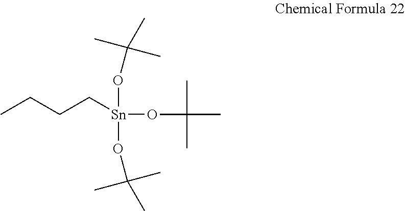
30 mL of anhydrous pentane was added to 10 g (35.4 mmol) of the compound represented by Chemical Formula 16 according to Synthesis Example 4 and then, cooled down to 0° C. 7.8 g (106.3 mmol) of diethylamine was slowly added thereto in a dropwise fashion, and subsequently 7.9 g (106.3 mmol) of tert-butanol was added thereto and then, stirred at 25° C. for 1 hour. When a reaction was complete, the resultant was filtered, concentrated, and vacuum-dried to obtain a compound represented by Chemical Formula 22 at a yield of 60%.
Figure US12158699-20241203-C00023
Synthesis Example 11
30 mL of anhydrous pentane was added to 10 g (37.3 mmol) of the compound represented by Chemical Formula 17 according to Synthesis Example 5 and then, cooled down to 0° C. 8.2 g (111.9 mmol) of diethylamine was slowly added thereto in a dropwise fashion, and subsequently, 6.7 g (111.9 mmol) of isopropanol was added thereto and then, stirred at 25° C. for 1 hour. When a reaction was complete, the resultant was filtered, concentrated, and vacuum-dried to obtain a compound represented by Chemical Formula 23 at a yield of 60%.
Figure US12158699-20241203-C00024
Synthesis Example 12
30 mL of anhydrous pentane was added to 10 g (18.7 mmol) of the compound represented by Chemical Formula 18 according to Synthesis Example 6 and then, cooled down to 0° C. 7.4 g (101.3 mmol) of diethylamine was slowly added thereto in a dropwise fashion, and subsequently, 6.1 g (101.3 mmol) of ethanol was added thereto and then, stirred at 25° C. for 1 hour. When a reaction was complete, the resultant was filtered, concentrated, and vacuum-dried to obtain a compound represented by Chemical Formula 24 at a yield of 60%.
Figure US12158699-20241203-C00025
Synthesis Example 13
10 g (25.4 mmol) of the compound represented by Chemical Formula 14 was put in a 100 mL round-bottomed flask, and 25 ml of formic acid was slowly added thereto in a dropwise fashion at 25° C. and then, heated and refluxed at 100° C. for 24 hours.
Subsequently, the temperature was decreased to 25° C., and then, the formic acid was vacuum distilled to obtain a compound represented by Chemical Formula 25 at a yield of 90%.
Figure US12158699-20241203-C00026
Examples 1 to 48
Each of the compounds represented by Chemical Formulas 19 to 25 obtained in Synthesis Examples 7 to 13, respectively, PAG-1 (San Apro, iodonium) or PAG-2 (Sigma-Aldrich, sulfonium), and lactic acid (Sigma-Aldrich) were dissolved in 4-methyl-2-pentanol, each at concentration of 3 wt % in the weight ratio shown in Tables 1 to 4, and were filtered with a 0.1 μm PTFE (polytetrafluoroethylene) syringe filter to prepare each of semiconductor photoresist compositions according to Examples 1 to 48.
A disk-shaped silicon wafer having a native-oxide surface and a 4 inch diameter was utilized as a substrate for thin film coating and treated in a UV ozone cleaning system for 10 minutes before coating the compositions. On the treated substrate, the semiconductor photoresist compositions according to Examples 1 to 48 were respectively spin-coated at 1500 rpm for 30 seconds and then, baked (baked after being applied, PAB (post-apply bake)) at 100° C. for 120 seconds to form a photoresist thin film.
After the coating and the baking, the thicknesses of the films were measured through ellipsometry, and were calculated to be about 25 nm.
TABLE 1
Example Example Example Example Example Example Example Example
1 2 3 4 5 6 7 8
Organic Chemical 99
metallic Formula19
compound Chemical 99
Formula20
Chemical 99 98
Formula21
Chemical 99
Formula22
Chemical 99
Formula23
Chemical 99
Formula24
Chemical 99
Formula25
PAG-1 1 1 1 1 1 1 1 1
Organic acid 1
(unit: parts by weight)
TABLE 2
Example Example Example Example Example Example Example Example
9 10 11 12 13 14 15 16
Organic Chemical 95
metallic Formula19
compound Chemical 95
Formula20
Chemical 95 94
Formula21
Chemical 95
Formula22
Chemical 95
Formula23
Chemical 95
Formula24
Chemical 95
Formula25
PAG-1 5 5 5 5 5 5 5 5
Organic acid 1
(unit: parts by weight)
TABLE 3
Example Example Example Example Example Example Example Example
17 18 19 20 21 22 23 24
Organic Chemical 90
metallic Formula19
compound Chemical 90
Formula20
Chemical 90 89
Formula21
Chemical 90
Formula22
Chemical 90
Formula23
Chemical 90
Formula24
Chemical 90
Formula25
PAG-1 10 10 10 10 10 10 10 10
Organic acid 1
(unit: parts by weight)
TABLE 4
Example Example Example Example Example Example Example Example
25 26 27 28 29 30 31 32
Organic Chemical 85
metallic Formula19
compound Chemical 85
Formula20
Chemical 85 84
Formula21
Chemical 85
Formula22
Chemical 85
Formula23
Chemical 85
Formula24
Chemical 85
Formula25
PAG-1 15 15 15 15 15 15 15 15
Organic acid 1
(unit: parts by weight)
TABLE 5
Example Example Example Example Example Example Example Example
33 34 35 36 37 38 39 40
Organic Chemical 99 95 90
metallic Formula19
compound Chemical 99 95 90
Formula20
Chemical 99 95
Formula21
Chemical
Formula22
Chemical
Formula23
Chemical
Formula24
Chemical
Formula25
PAG-2 1 1 1 5 5 5 10 10
Organic acid
(unit: parts by weight)
TABLE 6
Example Example Example Example Example Example Example Example
41 42 43 44 45 46 47 48
Organic Chemical 85
metallic Formula19
compound Chemical 85
Formula20
Chemical 90 85 98 94 89 84
Formula21
Chemical
Formula22
Chemical
Formula23
Chemical
Formula24
Chemical
Formula25
PAG-2 10 15 15 15 1 5 10 15
Organic acid 1 1 1 1
(unit: parts by weight)
Comparative Example 1
The compound represented by Chemical Formula 19 obtained in Synthesis Example 7 was dissolved in 4-methyl-2-pentanol at a concentration of 3 wt %, and was filtered with a 0.1 μm PTFE (polytetrafluoroethylene) syringe filter to prepare a semiconductor photoresist composition according to Comparative Example 1.
In substantially the same manner as in Example 1, a photoresist thin film including the semiconductor photoresist composition according to Comparative Example 1 was prepared. After the coating and baking, the thickness of the film was about 25 nm.
Comparative Example 2
A semiconductor photoresist composition according to Comparative Example 2 and a photoresist thin film including the same were manufactured according to substantially the same method as Comparative Example 1, except that nBuSnOOH (TCI Inc.) was utilized instead of the compound represented by Chemical Formula 19. After the coating and baking, the thickness of the film was about 25 nm.
Evaluation
The films according to Example 1 to Example 48, Comparative Example 1 and Comparative Example 2 (each formed on a disk-shaped silicon wafer utilizing the coating method) were exposed to extreme ultraviolet (EUV) light to form 12 to 100 nm line/space patterns by varying energy and a focus. After the exposure, the films were each baked at 180° C. for 120 seconds, subsequently, dipped in a Petri dish containing 2-heptanone for 60 seconds and taken out thereof, and washed with the same solvent for 10 seconds. Finally, the films were baked at 150° C. for 5 minutes, and then, pattern images thereof were obtained through SEM (scanning electron microscopy). From the SEM images, the highest resolution, optimal energy, and line edge roughness (LER) are provided Tables 7 and 8.
TABLE 7
Resolution (nm) Energy (mJ/cm2) LER (nm)
Example 1 11 65 1.7
Example 2 11 64 1.8
Example 3 10 65 1.6
Example 4 12 69 1.9
Example 5 12 68 1.9
Example 6 12 67 1.9
Example 7 11 65 1.7
Example 8 10 63 1.6
Example 9 11 52 1.6
Example 10 11 51 1.7
Example 11 10 52 1.5
Example 12 12 55 1.8
Example 13 12 54 1.8
Example 14 12 54 1.8
Example 15 11 52 1.6
Example 16 10 50 1.5
Example 17 11 42 1.6
Example 18 11 41 1.7
Example 19 10 42 1.5
Example 20 12 44 1.8
Example 21 12 44 1.8
Example 22 12 43 1.8
Example 23 11 42 1.6
Example 24 10 40 1.5
Example 25 11 37 1.8
Example 26 11 37 1.9
Example 27 10 37 1.7
Example 28 12 40 2.0
Example 29 12 39 2.0
Example 30 12 39 2.0
Example 31 11 37 1.8
Example 32 10 36 1.7
TABLE 8
Resolution (nm) Energy (mJ/cm2) LER (nm)
Example 33 11 65 1.7
Example 34 11 64 1.8
Example 35 10 65 1.6
Example 36 11 52 1.6
Example 37 11 51 1.7
Example 38 10 52 1.5
Example 39 11 42 1.6
Example 40 11 41 1.7
Example 41 10 42 1.5
Example 42 11 37 1.8
Example 43 11 37 1.9
Example 44 10 37 1.7
Example 45 10 63 1.6
Example 46 10 50 1.5
Example 47 10 40 1.5
Example 48 10 36 1.7
Comparative 14 78 2.6
Example 1
Comparative 18 102 4.1
Example 2
Referring to Tables 7 and 8, the photoresist thin films utilizing the semiconductor photoresist compositions according to Examples 1 to 48 exhibited excellent resolution, sensitivity, and line edge roughness (LER).
In contrast, photoresist thin films formed of the semiconductor photoresist composition of Comparative Example 1 that does not include the photoacid generator and includes the compound represented by Chemical Formula 19 alone, and the semiconductor photoresist composition of Comparative Example 2 that does not include the photoacid generator and includes nBuSnOOH (TCI Inc.), both exhibited higher resolution, optimal energy, and line edge roughness (LER) than those of Examples. Accordingly, the resolution, sensitivity, and line edge roughness (LER) thereof were not good compared with the Examples.
Hereinbefore, the certain embodiments of the present disclosure have been described and illustrated, however, it should be apparent to a person with ordinary skill in the art that the present disclosure is not limited to the embodiments as described, and may be variously modified and transformed without departing from the spirit and scope of the present disclosure. Accordingly, the modified or transformed embodiments as such may not be understood separately from the technical ideas and aspects of the present disclosure, and the modified embodiments are within the scope of the claims (and equivalents of the claims) of the present disclosure.
Description of symbols
100: substrate 102: thin film
104: resist underlayer 106: photoresist layer
106b: exposed region 106a: non-exposed region
108: photoresist pattern 112: organic layer pattern
114: thin film pattern

Claims (13)

What is claimed is:
1. A semiconductor photoresist composition comprising:
an organometallic compound represented by Chemical Formula 1,
an organometallic compound represented by Chemical Formula 7, an organometallic compound represented by Chemical Formula 8, or a combination thereof,
a photoacid generator (PAG),
an organic acid, and
a solvent,
wherein a weight ratio of the organometallic compound represented by Chemical Formula 7, the organometallic compound represented by Chemical Formula 8, or the sum of the compound represented by Chemical Formula 7 and the compound represented by Chemical Formula 8, to the organometallic compound represented by Chemical Formula 1 is about 1:1 to about 1:20:
Figure US12158699-20241203-C00027
wherein, in Chemical Formula 1,
R is a substituted or unsubstituted C1 to C20 alkyl group, a substituted or unsubstituted C3 to C20 cycloalkyl group, a substituted or unsubstituted C2 to C20 aliphatic unsaturated organic group including at least one double bond or triple bond, a substituted or unsubstituted C6 to C30 aryl group, an ethoxy group, a propoxy group, or a combination thereof,
X, Y, and Z are each independently —OC(═O)R2, and
R2 is hydrogen, a substituted or unsubstituted C1 to C20 alkyl group, a substituted or unsubstituted C3 to C20 cycloalkyl group, a substituted or unsubstituted C2 to C20 alkenyl group, a substituted or unsubstituted C2 to C20 alkynyl group, a substituted or unsubstituted C6 to C30 aryl group, or a combination thereof;
Figure US12158699-20241203-C00028
wherein, in Chemical Formula 7 and Chemical Formula 8,
Xa and Xb are each independently —OR12 or —OC(═O)R3,
R12 is a substituted or unsubstituted C1 to C20 alkyl group, a substituted or unsubstituted C3 to C20 cycloalkyl group, a substituted or unsubstituted C2 to C20 alkenyl group, a substituted or unsubstituted C2 to C20 alkynyl group, a substituted or unsubstituted C6 to C30 aryl group, or a combination thereof,
R13 is hydrogen, a substituted or unsubstituted C1 to C20 alkyl group, a substituted or unsubstituted C3 to C20 cycloalkyl group, a substituted or unsubstituted C2 to C20 alkenyl group, a substituted or unsubstituted C2 to C20 alkynyl group, a substituted or unsubstituted C6 to C30 aryl group, or a combination thereof,
M4 and M5 are each independently selected from the group consisting of tin (Sn), indium (In), and antimony (Sb), and
L is a single bond, a substituted or unsubstituted divalent C1 to C20 saturated aliphatic hydrocarbon group, a substituted or unsubstituted divalent C3 to C20 saturated or unsaturated alicyclic hydrocarbon group, a substituted or unsubstituted divalent C2 to C20 unsaturated aliphatic hydrocarbon group including at least one double bond or triple bond, a substituted or unsubstituted divalent C6 to C20 aromatic hydrocarbon group, —O—, —C(═O)—, or a combination thereof.
2. The semiconductor photoresist composition of claim 1, wherein the photoacid generator (PAG) comprises a cationic compound represented by Chemical Formula 2, Chemical Formula 3, or Chemical Formula 4:
Figure US12158699-20241203-C00029
wherein, in Chemical Formula 2 to Chemical Formula 4,
M1 is F, Cl, Br, or I,
M2 is O, S, Se, or Te,
M3 is N, P, As, or Sb, and
R3 to R11 are each independently a substituted or unsubstituted C1 to C20 alkyl group, a substituted or unsubstituted C3 to C20 cycloalkyl group, a substituted or unsubstituted C2 to C20 aliphatic unsaturated organic group including at least one double bond or triple bond, a substituted or unsubstituted C6 to C30 aryl group, or a combination thereof.
3. The semiconductor photoresist composition of claim 1, wherein the photoacid generator (PAG) comprises a cationic compound represented by Chemical Formula 5 or Chemical Formula 6:
Figure US12158699-20241203-C00030
and
wherein, in Chemical Formula 5 and Chemical Formula 6,
R3 to R7 are each independently a substituted or unsubstituted C1 to C20 alkyl group, a substituted or unsubstituted C3 to C20 cycloalkyl group, a substituted or unsubstituted C2 to C20 aliphatic unsaturated organic group including at least one double bond or triple bond, a substituted or unsubstituted C6 to C30 aryl group, or a combination thereof.
4. The semiconductor photoresist composition of claim 1, wherein the organometallic compound represented by Chemical Formula 1 and the photoacid generator (PAG) are in a weight ratio of about 99:1 to about 60:40.
5. The semiconductor photoresist composition of claim 1, wherein the organometallic compound represented by Chemical Formula 1 and the photoacid generator (PAG) are in a weight ratio of about 95:5 to about 85:15.
6. The semiconductor photoresist composition of claim 1, wherein
R is a substituted or unsubstituted C1 to C8 alkyl group, a substituted or unsubstituted C3 to C8 cycloalkyl group, a substituted or unsubstituted C2 to C8 aliphatic unsaturated organic group including at least one double bond or triple bond, a substituted or unsubstituted C6 to C20 aryl group, an ethoxy group, a propoxy group, or a combination thereof,
R2 is hydrogen, a substituted or unsubstituted C1 to C8 alkyl group, a substituted or unsubstituted C3 to C8 cycloalkyl group, a substituted or unsubstituted C2 to C8 alkenyl group, a substituted or unsubstituted C2 to C8 alkynyl group, a substituted or unsubstituted C6 to C20 aryl group, or a combination thereof.
7. The semiconductor photoresist composition of claim 1, wherein
R is a methyl group, an ethyl group, a propyl group, a butyl group, an isopropyl group, a tert-butyl group, a 2,2-dimethylpropyl group, a cyclopropyl group, a cyclobutyl group, a cyclopentyl group, a cyclohexyl group, an ethenyl group, a propenyl group, a butenyl group, an ethynyl group, a propynyl group, a butynyl group, a phenyl group, a tolyl group, a xylene group, a benzyl group, an ethoxy group, a propoxy group, or a combination thereof,
and
R2 is hydrogen, a methyl group, an ethyl group, a propyl group, a butyl group, an isopropyl group, a tert-butyl group, a 2,2-dimethylpropyl group, a cyclopropyl group, a cyclobutyl group, a cyclopentyl group, a cyclohexyl group, an ethenyl group, a propenyl group, a butenyl group, an ethynyl group, a propynyl group, a butynyl group, a phenyl group, a tolyl group, a xylene group, a benzyl group, or a combination thereof.
8. The semiconductor photoresist composition of claim 1, wherein the organometallic compound represented by Chemical Formula 1 comprises a compound represented by Chemical Formula 10:
Figure US12158699-20241203-C00031
wherein, in Chemical Formula 10,
R is a substituted or unsubstituted C1 to C20 alkyl group, a substituted or unsubstituted C3 to C20 cycloalkyl group, a substituted or unsubstituted C2 to C20 aliphatic unsaturated organic group including at least one double bond or triple bond, a substituted or unsubstituted C6 to C30 aryl group, an ethoxy group, a propoxy group, or a combination thereof,
and
Rd, Re, and Rf are each independently hydrogen, a substituted or unsubstituted C1 to C20 alkyl group, a substituted or unsubstituted C3 to C20 cycloalkyl group, a substituted or unsubstituted C2 to C20 alkenyl group, a substituted or unsubstituted C2 to C20 alkynyl group, a substituted or unsubstituted C6 to C30 aryl group, or a combination thereof.
9. The semiconductor photoresist composition of claim 1, wherein the semiconductor photoresist composition further comprises an additive selected from the group consisting of a surfactant, a cross-linking agent, a leveling agent, a quencher, and combinations thereof.
10. A method of forming patterns, the method comprising:
forming an etching-objective layer on a substrate,
coating the semiconductor photoresist composition of claim 1 on the etching-objective layer to form a photoresist layer,
patterning the photoresist layer to form a photoresist pattern, and
etching the etching-objective layer utilizing the photoresist pattern as an etching mask.
11. The method of claim 10, wherein the photoresist pattern is formed utilizing light in a wavelength of about 5 nm to about 150 nm.
12. The method of claim 10, further comprising providing a resist underlayer between the substrate and the photoresist layer.
13. The method of claim 10, wherein the photoresist pattern has a width of about 5 nm to about 100 nm.
US17/217,941 2020-04-02 2021-03-30 Semiconductor photoresist composition and method of forming patterns using the composition Active 2043-03-17 US12158699B2 (en)

Applications Claiming Priority (2)

Application Number Priority Date Filing Date Title
KR1020200040507A KR102573327B1 (en) 2020-04-02 2020-04-02 Semiconductor photoresist composition and method of forming patterns using the composition
KR10-2020-0040507 2020-04-02

Publications (2)

Publication Number Publication Date
US20210311387A1 US20210311387A1 (en) 2021-10-07
US12158699B2 true US12158699B2 (en) 2024-12-03

Family

ID=77922729

Family Applications (1)

Application Number Title Priority Date Filing Date
US17/217,941 Active 2043-03-17 US12158699B2 (en) 2020-04-02 2021-03-30 Semiconductor photoresist composition and method of forming patterns using the composition

Country Status (5)

Country Link
US (1) US12158699B2 (en)
JP (1) JP7168715B2 (en)
KR (1) KR102573327B1 (en)
CN (1) CN113495429A (en)
TW (1) TWI784459B (en)

Families Citing this family (21)

* Cited by examiner, † Cited by third party
Publication number Priority date Publication date Assignee Title
US11609494B2 (en) * 2019-04-30 2023-03-21 Samsung Sdi Co., Ltd. Semiconductor photoresist composition and method of forming patterns using the composition
KR102573327B1 (en) 2020-04-02 2023-08-30 삼성에스디아이 주식회사 Semiconductor photoresist composition and method of forming patterns using the composition
KR102619719B1 (en) * 2020-05-12 2023-12-28 삼성에스디아이 주식회사 Semiconductor photoresist composition and method of forming patterns using the composition
KR102690557B1 (en) 2020-12-18 2024-07-30 삼성에스디아이 주식회사 Semiconductor photoresist composition, method for preparing thereof and method of forming patterns using the composition
KR102598259B1 (en) * 2020-12-18 2023-11-02 삼성에스디아이 주식회사 Semiconductor photoresist composition and method of forming patterns using the composition
US11827659B2 (en) * 2022-03-31 2023-11-28 Feng Lu Organometallic tin compounds as EUV photoresist
US20230341773A1 (en) * 2022-04-21 2023-10-26 Taiwan Semiconductor Manufacturing Company, Ltd. Photoresist composition with novel solvent
KR102703674B1 (en) * 2022-08-02 2024-09-04 삼성에스디아이 주식회사 Semiconductor photoresist composition and method of forming patterns using the composition
IL305619A (en) 2022-09-14 2024-04-01 Shinetsu Chemical Co Compound for forming metal-containing film, composition for forming metal-containing film, patterning process, and semiconductor photoresist material
KR102710054B1 (en) * 2022-09-16 2024-09-24 삼성에스디아이 주식회사 Semiconductor photoresist composition and method of forming patterns using the composition
JP2024089633A (en) 2022-12-21 2024-07-03 信越化学工業株式会社 Polymer for forming metal-containing film, composition for forming metal-containing film, and method for forming pattern
KR20240103837A (en) * 2022-12-27 2024-07-04 삼성전자주식회사 Resist composition comprising the same and method of forming pattern using the same
KR20240103838A (en) * 2022-12-27 2024-07-04 삼성전자주식회사 Resist composition comprising the same and method of forming pattern using the same
JP7802711B2 (en) 2023-01-06 2026-01-20 信越化学工業株式会社 Compound for forming metal-containing film, composition for forming metal-containing film, and pattern forming method
JP7802029B2 (en) 2023-02-15 2026-01-19 信越化学工業株式会社 Compound for forming metal-containing film, composition for forming metal-containing film, pattern forming method
CN116675713B (en) * 2023-05-15 2025-07-29 上海大学 Tin-containing polymerizable photoacid generator and preparation method thereof
JP2025032875A (en) 2023-08-28 2025-03-12 信越化学工業株式会社 Compound for forming metal-containing film, composition for forming metal-containing film, and method for forming pattern
JP2025032887A (en) 2023-08-28 2025-03-12 信越化学工業株式会社 Compound for forming metal-containing film, composition for forming metal-containing film, and method for forming pattern
KR102852077B1 (en) * 2023-11-20 2025-08-28 성균관대학교산학협력단 A composition for photoresist containing antimony-based organometallic compounds and a method of forming a photoresist pattern using the composition
JP2025099570A (en) 2023-12-22 2025-07-03 信越化学工業株式会社 Compound for forming metal-containing film, composition for forming metal-containing film, and patterning process
JP2025099887A (en) 2023-12-22 2025-07-03 信越化学工業株式会社 Compound for forming metal-containing film, composition for forming metal-containing film, and patterning process

Citations (58)

* Cited by examiner, † Cited by third party
Publication number Priority date Publication date Assignee Title
US2826597A (en) 1953-01-22 1958-03-11 Metal & Thermit Corp Stabilizer for resins
US2832751A (en) 1951-06-21 1958-04-29 Metal & Thermit Corp Polyvinyl chloride stabilized with butyl tin s, s', s" tris
US5061599A (en) 1986-06-11 1991-10-29 Hitachi, Ltd. Radiation sensitive materials
KR950001702B1 (en) 1992-04-16 1995-02-28 한국과학기술연구원 Organotinmalonates derivatives, and process for their preparation
JPH08260159A (en) 1994-12-09 1996-10-08 Mitsubishi Materials Corp Composition for forming metal oxide thin film pattern, method for producing the same, method for forming metal oxide thin film pattern, and method for producing electronic component and optical component
US6103448A (en) 1997-10-08 2000-08-15 Korea Advanced Institute Of Science And Technology Organometal-containing acrylate or methacrylate derivatives and photoresists containing the polymers thereof
KR20020041759A (en) 2000-11-28 2002-06-03 마티네즈 길러모 Photoresist composition
US20020072009A1 (en) 2000-12-13 2002-06-13 Kim Hyun-Woo Photosensitive polymer containing Si, Ge or Sn and resist composition comprising the same
US6514666B1 (en) 1999-11-05 2003-02-04 Hyundai Electronics Industries Co., Ltd. Photoresist monomers, polymers thereof and photoresist compositions containing it
US6607867B1 (en) 2000-06-30 2003-08-19 Korea Advanced Institute Of Science And Technology Organometal-containing norbornene monomer, photoresist containing its polymer, manufacturing method thereof, and method of forming photoresist patterns
KR100386719B1 (en) 1996-12-19 2004-05-22 주식회사 코오롱 Diazo type photosensitive film
JP2009134088A (en) * 2007-11-30 2009-06-18 Jsr Corp Radiation sensitive resin composition
JP2009229593A (en) 2008-03-19 2009-10-08 Mitsuboshi Belting Ltd Ink composition for repairing photomask, and photomask repairing method
US20110045406A1 (en) 2006-11-01 2011-02-24 State of Oregon acting by and through the State Board of Higher Education on behalf of Oregon Solution processed thin films and laminates, devices comprising such thin films and laminates, and method for their use and manufacture
US20110293888A1 (en) 2010-06-01 2011-12-01 Stowers Jason K Patterned inorganic layers, radiation based patterning compositions and corresponding methods
JP4831324B2 (en) 2006-07-06 2011-12-07 日産化学工業株式会社 Resist underlayer film forming composition containing sulfone
US20120208127A1 (en) 2011-02-15 2012-08-16 Shin-Etsu Chemical Co., Ltd. Resist composition and patterning process
US20130005150A1 (en) 2011-06-28 2013-01-03 Shin-Etsu Chemical Co., Ltd. Composition for forming resist underlayer film and patterning process using the same
JP5178858B2 (en) 2003-03-03 2013-04-10 ローム・アンド・ハース・エレクトロニック・マテリアルズ,エル.エル.シー. Polymer and photoresist containing the same
US20130224652A1 (en) 2012-02-27 2013-08-29 International Business Machines Corporation Metal peroxo compounds with organic co-ligands for electron beam, deep uv and extreme uv photoresist applications
KR101486533B1 (en) 2013-09-16 2015-02-09 한국기계연구원 Method for manufacturing quantum dot and method for manufacturing solar cell using the same
US20160116839A1 (en) 2014-10-23 2016-04-28 Inpria Corporation Organometallic solution based high resolution patterning compositions and corresponding methods
WO2016140057A1 (en) 2015-03-05 2016-09-09 Jsr株式会社 Radiation-sensitive composition and pattern formation method
US20160310944A1 (en) 2015-04-21 2016-10-27 Jsr Corporation Method of producing microfluidic device, microfluidic device, and photosensitive resin composition
US20170052449A1 (en) 2015-08-20 2017-02-23 Osaka University Chemically amplified resist material, pattern-forming method, compound, and production method of compound
US20170102612A1 (en) 2015-10-13 2017-04-13 Inpria Corporation Organotin oxide hydroxide patterning compositions, precursors, and patterning
WO2017169440A1 (en) 2016-03-28 2017-10-05 Jsr株式会社 Radiation-sensitive composition and pattern formation method
JP2017207532A (en) 2016-05-16 2017-11-24 東洋合成工業株式会社 Resist composition and method for producing device using the same
WO2017204090A1 (en) * 2016-05-26 2017-11-30 Jsr株式会社 Radiation-sensitive composition and pattern forming method
KR20170132726A (en) 2015-04-01 2017-12-04 도레이 카부시키가이샤 Photosensitive resin composition, method of manufacturing conductive pattern, substrate, touch panel and display
JP2018017780A (en) 2016-07-25 2018-02-01 Jsr株式会社 Radiation-sensitive composition and pattern formation method
US20180046086A1 (en) 2016-08-12 2018-02-15 Inpria Corporation Methods of reducing metal residue in edge bead region from metal-containing resists
WO2018043506A1 (en) 2016-08-29 2018-03-08 Jsr株式会社 Radiation sensitive composition and pattern forming method
WO2018046438A1 (en) 2016-09-07 2018-03-15 Ivoclar Vivadent Ag Polymerizable compositions comprising acyl tin photoinitiators
KR20180043170A (en) 2016-10-19 2018-04-27 롬엔드하스전자재료코리아유한회사 Photosensitive resin composition and cured film prepared therefrom
JP2018116160A (en) * 2017-01-18 2018-07-26 Jsr株式会社 Radiation-sensitive composition and pattern forming method
WO2018168221A1 (en) 2017-03-13 2018-09-20 Jsr株式会社 Radiation sensitive composition and pattern forming method
WO2018179704A1 (en) 2017-03-27 2018-10-04 Jsr株式会社 Pattern forming method
TW201920214A (en) 2017-08-02 2019-06-01 加拿大商海星化工無限責任公司 Organometallic compounds and methods for the deposition of high purity tin oxide
TW201924927A (en) 2017-11-17 2019-07-01 日商三井化學股份有限公司 Semiconductor device intermediate, composition for formation of metal-containing film, method of manufacturing semiconductor device intermediate, and method of manufacturing semiconductor device
KR20190082279A (en) 2016-11-07 2019-07-09 도요 고세이 고교 가부시키가이샤 Metal-containing onium salt compounds, photo-degradable bases and resist compositions, and methods of manufacturing devices using the resist compositions
TWI669353B (en) 2015-02-11 2019-08-21 盧森堡商Az電子材料(盧森堡)股份有限公司 Metal hardmask composition and processes for forming fine patterns on semiconductor substrates
JP2019183150A (en) 2018-03-30 2019-10-24 住友化学株式会社 Mixed composition
US20190384171A1 (en) 2018-06-15 2019-12-19 Taiwan Semiconductor Manufacturing Co., Ltd. Photoresist composition and method of forming photoresist pattern
KR20200005370A (en) 2018-07-06 2020-01-15 삼성에스디아이 주식회사 Semiconductor resist composition, and method of forming patterns using the composition
US20200041901A1 (en) 2018-07-31 2020-02-06 Samsung Sdi Co., Ltd. Semiconductor resist composition, and method of forming patterns using the composition
JP2020021071A (en) * 2018-07-31 2020-02-06 三星エスディアイ株式会社Samsung SDI Co., Ltd. Semiconductor resist composition and pattern forming method using the same
US20200041896A1 (en) * 2018-07-31 2020-02-06 Samsung Sdi Co., Ltd. Semiconductor resist composition, and method of forming patterns using the composition
KR20200014216A (en) 2018-07-31 2020-02-10 삼성에스디아이 주식회사 Semiconductor resist composition, and method of forming patterns using the composition
KR20200014185A (en) 2018-07-31 2020-02-10 삼성에스디아이 주식회사 Semiconductor resist composition, and method of forming patterns using the composition
KR20200018080A (en) 2018-08-10 2020-02-19 삼성에스디아이 주식회사 Semiconductor resist composition, and method of forming patterns using the composition
US20200073238A1 (en) 2018-08-31 2020-03-05 Taiwan Semiconductor Manufacturing Co., Ltd. Photoresist, developer, and method of forming photoresist pattern
US20200117085A1 (en) 2018-07-31 2020-04-16 Samsung Sdi Co., Ltd. Semiconductor resist composition, and method of forming patterns using the composition
US20200124970A1 (en) * 2018-10-17 2020-04-23 Inpria Corporation Patterned organometallic photoresists and methods of patterning
CN111856879A (en) 2019-04-30 2020-10-30 三星Sdi株式会社 Semiconductor photoresist composition and method of patterning using the composition
US20210311387A1 (en) 2020-04-02 2021-10-07 Samsung Sdi Co., Ltd. Semiconductor photoresist composition and method of forming patterns using the composition
US20210356861A1 (en) * 2020-05-12 2021-11-18 Samsung Sdi Co., Ltd. Semiconductor photoresist composition and method of forming patterns using the composition
US20240027899A1 (en) * 2022-07-12 2024-01-25 Samsung Sdi Co., Ltd Semiconductor photoresist composition and method of forming patterns using the composition

Patent Citations (83)

* Cited by examiner, † Cited by third party
Publication number Priority date Publication date Assignee Title
US2832751A (en) 1951-06-21 1958-04-29 Metal & Thermit Corp Polyvinyl chloride stabilized with butyl tin s, s', s" tris
US2826597A (en) 1953-01-22 1958-03-11 Metal & Thermit Corp Stabilizer for resins
US5061599A (en) 1986-06-11 1991-10-29 Hitachi, Ltd. Radiation sensitive materials
KR950001702B1 (en) 1992-04-16 1995-02-28 한국과학기술연구원 Organotinmalonates derivatives, and process for their preparation
JPH08260159A (en) 1994-12-09 1996-10-08 Mitsubishi Materials Corp Composition for forming metal oxide thin film pattern, method for producing the same, method for forming metal oxide thin film pattern, and method for producing electronic component and optical component
KR100386719B1 (en) 1996-12-19 2004-05-22 주식회사 코오롱 Diazo type photosensitive film
US6103448A (en) 1997-10-08 2000-08-15 Korea Advanced Institute Of Science And Technology Organometal-containing acrylate or methacrylate derivatives and photoresists containing the polymers thereof
KR100269513B1 (en) 1997-10-08 2000-10-16 윤덕용 New acrylate or methacrylate derivatives and photoresist containing its polymer
US6514666B1 (en) 1999-11-05 2003-02-04 Hyundai Electronics Industries Co., Ltd. Photoresist monomers, polymers thereof and photoresist compositions containing it
US6607867B1 (en) 2000-06-30 2003-08-19 Korea Advanced Institute Of Science And Technology Organometal-containing norbornene monomer, photoresist containing its polymer, manufacturing method thereof, and method of forming photoresist patterns
KR100398312B1 (en) 2000-06-30 2003-09-19 한국과학기술원 Organometal-containing norbornene monomer, photoresist containing its polymer, manufacturing methods thereof, and method of forming photoresist patterns
KR20020041759A (en) 2000-11-28 2002-06-03 마티네즈 길러모 Photoresist composition
US20020072009A1 (en) 2000-12-13 2002-06-13 Kim Hyun-Woo Photosensitive polymer containing Si, Ge or Sn and resist composition comprising the same
JP3990146B2 (en) 2000-12-13 2007-10-10 三星電子株式会社 Photosensitive polymer containing silicon and resist composition containing the same
JP5178858B2 (en) 2003-03-03 2013-04-10 ローム・アンド・ハース・エレクトロニック・マテリアルズ,エル.エル.シー. Polymer and photoresist containing the same
JP4831324B2 (en) 2006-07-06 2011-12-07 日産化学工業株式会社 Resist underlayer film forming composition containing sulfone
US20110045406A1 (en) 2006-11-01 2011-02-24 State of Oregon acting by and through the State Board of Higher Education on behalf of Oregon Solution processed thin films and laminates, devices comprising such thin films and laminates, and method for their use and manufacture
JP2009134088A (en) * 2007-11-30 2009-06-18 Jsr Corp Radiation sensitive resin composition
JP2009229593A (en) 2008-03-19 2009-10-08 Mitsuboshi Belting Ltd Ink composition for repairing photomask, and photomask repairing method
US20110293888A1 (en) 2010-06-01 2011-12-01 Stowers Jason K Patterned inorganic layers, radiation based patterning compositions and corresponding methods
CN102269929A (en) 2010-06-01 2011-12-07 因普利亚公司 Patterned inorganic layers, radiation based patterning compositions and corresponding methods
JP2018041099A (en) 2010-06-01 2018-03-15 インプリア・コーポレイションInpria Corporation Patterned inorganic layers, radiation based patterning compositions and corresponding methods
JP5708521B2 (en) 2011-02-15 2015-04-30 信越化学工業株式会社 Resist material and pattern forming method using the same
US20120208127A1 (en) 2011-02-15 2012-08-16 Shin-Etsu Chemical Co., Ltd. Resist composition and patterning process
JP5650086B2 (en) 2011-06-28 2015-01-07 信越化学工業株式会社 Resist underlayer film forming composition and pattern forming method
US20130005150A1 (en) 2011-06-28 2013-01-03 Shin-Etsu Chemical Co., Ltd. Composition for forming resist underlayer film and patterning process using the same
KR20140121826A (en) 2012-02-27 2014-10-16 인터내셔널 비지네스 머신즈 코포레이션 Metal peroxo compounds with organic co-ligands for electron beam, deep uv and extreme uv photoresist applications
US20130224652A1 (en) 2012-02-27 2013-08-29 International Business Machines Corporation Metal peroxo compounds with organic co-ligands for electron beam, deep uv and extreme uv photoresist applications
KR101486533B1 (en) 2013-09-16 2015-02-09 한국기계연구원 Method for manufacturing quantum dot and method for manufacturing solar cell using the same
US20160116839A1 (en) 2014-10-23 2016-04-28 Inpria Corporation Organometallic solution based high resolution patterning compositions and corresponding methods
JP2018502173A (en) 2014-10-23 2018-01-25 インプリア・コーポレイションInpria Corporation High resolution patterning compositions based on organometallic solutions and corresponding methods
TWI669353B (en) 2015-02-11 2019-08-21 盧森堡商Az電子材料(盧森堡)股份有限公司 Metal hardmask composition and processes for forming fine patterns on semiconductor substrates
WO2016140057A1 (en) 2015-03-05 2016-09-09 Jsr株式会社 Radiation-sensitive composition and pattern formation method
TWI684063B (en) 2015-03-05 2020-02-01 日商Jsr股份有限公司 Radiation sensitive composition and pattern forming method
KR20170132726A (en) 2015-04-01 2017-12-04 도레이 카부시키가이샤 Photosensitive resin composition, method of manufacturing conductive pattern, substrate, touch panel and display
US20160310944A1 (en) 2015-04-21 2016-10-27 Jsr Corporation Method of producing microfluidic device, microfluidic device, and photosensitive resin composition
TWI684068B (en) 2015-04-21 2020-02-01 日商Jsr股份有限公司 Microfluidic device manufacturing method, microfluidic device, and photosensitive resin composition for microfluidic device manufacturing
US20170052449A1 (en) 2015-08-20 2017-02-23 Osaka University Chemically amplified resist material, pattern-forming method, compound, and production method of compound
KR20170022945A (en) 2015-08-20 2017-03-02 고꾸리쯔 다이가꾸 호우징 오사까 다이가꾸 Chemically amplified resist material, pattern-forming method, compound, and production method of compound
US20170102612A1 (en) 2015-10-13 2017-04-13 Inpria Corporation Organotin oxide hydroxide patterning compositions, precursors, and patterning
JP2019500490A (en) 2015-10-13 2019-01-10 インプリア・コーポレイションInpria Corporation Organotin oxide hydroxide patterning compositions, precursors and patterning
CN108351594A (en) 2015-10-13 2018-07-31 因普里亚公司 Organotin oxide hydroxide patterning composition, precursor and patterning
WO2017169440A1 (en) 2016-03-28 2017-10-05 Jsr株式会社 Radiation-sensitive composition and pattern formation method
US20190033713A1 (en) 2016-03-28 2019-01-31 Jsr Corporation Radiation-sensitive composition and pattern-forming method
JP2017207532A (en) 2016-05-16 2017-11-24 東洋合成工業株式会社 Resist composition and method for producing device using the same
WO2017204090A1 (en) * 2016-05-26 2017-11-30 Jsr株式会社 Radiation-sensitive composition and pattern forming method
JP2018017780A (en) 2016-07-25 2018-02-01 Jsr株式会社 Radiation-sensitive composition and pattern formation method
US20180046086A1 (en) 2016-08-12 2018-02-15 Inpria Corporation Methods of reducing metal residue in edge bead region from metal-containing resists
KR20190045162A (en) 2016-08-29 2019-05-02 제이에스알 가부시끼가이샤 A radiation-sensitive composition and a method for forming a pattern
WO2018043506A1 (en) 2016-08-29 2018-03-08 Jsr株式会社 Radiation sensitive composition and pattern forming method
US20190227432A1 (en) 2016-08-29 2019-07-25 Jsr Corporation Radiation-sensitive composition and pattern-forming method
WO2018046438A1 (en) 2016-09-07 2018-03-15 Ivoclar Vivadent Ag Polymerizable compositions comprising acyl tin photoinitiators
KR20180043170A (en) 2016-10-19 2018-04-27 롬엔드하스전자재료코리아유한회사 Photosensitive resin composition and cured film prepared therefrom
KR20190082279A (en) 2016-11-07 2019-07-09 도요 고세이 고교 가부시키가이샤 Metal-containing onium salt compounds, photo-degradable bases and resist compositions, and methods of manufacturing devices using the resist compositions
US20190243243A1 (en) 2016-11-07 2019-08-08 Toyo Gosei Co., Ltd. Metal-containing onium salt compound, photodegradable base, resist composition, and method for manufacturing device using said resist composition
JP2018116160A (en) * 2017-01-18 2018-07-26 Jsr株式会社 Radiation-sensitive composition and pattern forming method
WO2018168221A1 (en) 2017-03-13 2018-09-20 Jsr株式会社 Radiation sensitive composition and pattern forming method
WO2018179704A1 (en) 2017-03-27 2018-10-04 Jsr株式会社 Pattern forming method
TW201920214A (en) 2017-08-02 2019-06-01 加拿大商海星化工無限責任公司 Organometallic compounds and methods for the deposition of high purity tin oxide
US20190337969A1 (en) 2017-08-02 2019-11-07 Seastar Chemicals Inc. Organometallic compounds and methods for the deposition of high purity tin oxide
TW201924927A (en) 2017-11-17 2019-07-01 日商三井化學股份有限公司 Semiconductor device intermediate, composition for formation of metal-containing film, method of manufacturing semiconductor device intermediate, and method of manufacturing semiconductor device
JP2019183150A (en) 2018-03-30 2019-10-24 住友化学株式会社 Mixed composition
US20190384171A1 (en) 2018-06-15 2019-12-19 Taiwan Semiconductor Manufacturing Co., Ltd. Photoresist composition and method of forming photoresist pattern
KR20200005370A (en) 2018-07-06 2020-01-15 삼성에스디아이 주식회사 Semiconductor resist composition, and method of forming patterns using the composition
US20200041901A1 (en) 2018-07-31 2020-02-06 Samsung Sdi Co., Ltd. Semiconductor resist composition, and method of forming patterns using the composition
US11092890B2 (en) * 2018-07-31 2021-08-17 Samsung Sdi Co., Ltd. Semiconductor resist composition, and method of forming patterns using the composition
US20200041896A1 (en) * 2018-07-31 2020-02-06 Samsung Sdi Co., Ltd. Semiconductor resist composition, and method of forming patterns using the composition
KR20200014216A (en) 2018-07-31 2020-02-10 삼성에스디아이 주식회사 Semiconductor resist composition, and method of forming patterns using the composition
KR20200014043A (en) 2018-07-31 2020-02-10 삼성에스디아이 주식회사 Semiconductor resist composition, and method of forming patterns using the composition
KR20200014185A (en) 2018-07-31 2020-02-10 삼성에스디아이 주식회사 Semiconductor resist composition, and method of forming patterns using the composition
CN110780536A (en) 2018-07-31 2020-02-11 三星Sdi株式会社 Semiconductor resist composition and method and system for forming pattern using the same
TW202007691A (en) 2018-07-31 2020-02-16 南韓商三星Sdi股份有限公司 Semiconductor resist composition, and method and system of forming patterns using the composition
JP2020021071A (en) * 2018-07-31 2020-02-06 三星エスディアイ株式会社Samsung SDI Co., Ltd. Semiconductor resist composition and pattern forming method using the same
US20200117085A1 (en) 2018-07-31 2020-04-16 Samsung Sdi Co., Ltd. Semiconductor resist composition, and method of forming patterns using the composition
KR20200018080A (en) 2018-08-10 2020-02-19 삼성에스디아이 주식회사 Semiconductor resist composition, and method of forming patterns using the composition
US20200073238A1 (en) 2018-08-31 2020-03-05 Taiwan Semiconductor Manufacturing Co., Ltd. Photoresist, developer, and method of forming photoresist pattern
US20200124970A1 (en) * 2018-10-17 2020-04-23 Inpria Corporation Patterned organometallic photoresists and methods of patterning
CN111856879A (en) 2019-04-30 2020-10-30 三星Sdi株式会社 Semiconductor photoresist composition and method of patterning using the composition
JP2020184074A (en) 2019-04-30 2020-11-12 三星エスディアイ株式会社Samsung SDI Co., Ltd. Semiconductor photoresist composition and method of forming patterns using the composition
US11609494B2 (en) * 2019-04-30 2023-03-21 Samsung Sdi Co., Ltd. Semiconductor photoresist composition and method of forming patterns using the composition
US20210311387A1 (en) 2020-04-02 2021-10-07 Samsung Sdi Co., Ltd. Semiconductor photoresist composition and method of forming patterns using the composition
US20210356861A1 (en) * 2020-05-12 2021-11-18 Samsung Sdi Co., Ltd. Semiconductor photoresist composition and method of forming patterns using the composition
US20240027899A1 (en) * 2022-07-12 2024-01-25 Samsung Sdi Co., Ltd Semiconductor photoresist composition and method of forming patterns using the composition

Non-Patent Citations (21)

* Cited by examiner, † Cited by third party
Title
Anderson, Christopher N., et al.; "The Sematech Berkeley MET: extending EUV learning down to 16nm half pitch"; Proc. of SPIE; vol. 7969, 79690R (2011); (7 pages).
Chinese Office Action (including a search report) dated Mar. 29, 2024, of the corresponding Chinese Patent Application No. 202110349838.1 (7 pages).
Japanese Notice of Reasons for Rejection dated Nov. 15, 2022 issued in JP Application No. 2021-183873 (3 pages).
Japanese Office Action for JP Application No. 2021-056503 dated Mar. 29, 2022, 3 pages.
JPO Office action dated May 18, 2021 issued in corresponding JP Application No. 2020-080534, 4 pages.
Korean Office Action dated May 12, 2023, issued in Korean Patent Application No. 10-2020-0040507 (7 pages).
Korean Office Action dated May 12, 2023, issued in Korean Patent Application No. 10-2020-0056720 (7 pages).
Non-Final Rejection issued in related U.S. Appl. No. 16/859,682, dated Dec. 20, 2021, 12 pages.
Notice of Allowance dated Apr. 13, 2022 in U.S. Appl. No. 16/859,682, 8 pages.
Notice of Reason for Rejection for JP Application No. 2021-078454 dated Jun. 7, 2022, 3 pages.
Okamoto, Hiroshi et al., "Peroxypolytungstic acids: A new inorganic resist material", Applied Physics Letters, Aug. 4, 1986, 49 (5), pp. 298-300.
Stowers, Jason K. et al., "Directly patterned inorganic hardmask for EUV lithography,", Proc. of SPIE, vol. 7969, Extreme Ultraviolet (EUV) Lithography II, 796915, 2011, 11pp.
Taiwanese Office Action dated Nov. 8, 2021, in Taiwanese Patent Application No. 109114182 and accompanying Search Report (6 pages).
Taiwanese Office Action for TW Application No. 110111615 dated Apr. 29, 2022, 5 pages.
Taiwanese Search Report dated Jun. 25, 2022, for Application No. 110143319, 2 pages.
TW Office Action and Search Report dated Nov. 16, 2021 in corresponding Taiwanese Patent Application No. 110116951, 7 pages.
US Notice of Allowance dated Jul. 29, 2022, issued in U.S. Appl. No. 16/859,682 (7 pages).
US Notice of Allowance dated Nov. 9, 2022, issued in U.S. Appl. No. 16/859,682 (7 pages).
US Office Action dated Mar. 24, 2023, issued in U.S. Appl. No. 17/454,453 (17 pages).
US Office Action dated May 10, 2023, issued in U.S. Appl. No. 17/306,820 (8 pages).
US Restriction Requirement dated Jan. 3, 2023, issued in U.S. Appl. No. 17/306,820 (6 pages).

Also Published As

Publication number Publication date
KR20210123138A (en) 2021-10-13
JP7168715B2 (en) 2022-11-09
KR102573327B1 (en) 2023-08-30
TW202138380A (en) 2021-10-16
JP2021162865A (en) 2021-10-11
CN113495429A (en) 2021-10-12
TWI784459B (en) 2022-11-21
US20210311387A1 (en) 2021-10-07

Similar Documents

Publication Publication Date Title
US12158699B2 (en) Semiconductor photoresist composition and method of forming patterns using the composition
US12306534B2 (en) Semiconductor photoresist composition and method of forming patterns using the composition
US11609494B2 (en) Semiconductor photoresist composition and method of forming patterns using the composition
US11415885B2 (en) Semiconductor photoresist composition, and method of forming patterns using the composition
US11092890B2 (en) Semiconductor resist composition, and method of forming patterns using the composition
US12538761B2 (en) Composition for semiconductor photoresist, and pattern formation method using same
US20240027899A1 (en) Semiconductor photoresist composition and method of forming patterns using the composition
US20240061336A1 (en) Semiconductor photoresist composition and method of forming patterns using the composition
US20240168375A1 (en) Semiconductor photoresist composition and method of forming patters using the composition
US20250044686A1 (en) Method of forming patterns
US20250054758A1 (en) Semiconductor photoresist composition and method of forming patterns using the composition
US20240176234A1 (en) Semiconductor photoresist composition and method of forming patterns using the composition
US20250306456A1 (en) Semiconductor photoresist compositions and methods of forming patterns using the composition
US20250102907A1 (en) Semiconductor photoresist composition and method of forming patterns using the composition
US20250306457A1 (en) Semiconductor photoresist compositions and methods of forming patterns using the composition
US20250264798A1 (en) Semiconductor photoresist compositions and methods of forming patterns using the composition
US20250298311A1 (en) Semiconductor photoresist composition and methods of forming patterns using the composition
US20250068066A1 (en) Semiconductor photoresist composition and method of forming patterns using the composition
US20250224669A1 (en) Method of forming patterns and photoresist film
US20250263427A1 (en) Semiconductor photoresist compositions and methods of forming patterns using the composition
US20250216777A1 (en) Semiconductor photoresist composition and method of forming patterns using the composition
US20250355348A1 (en) Semiconductor photoresist compositions and methods of forming patterns using the compositions
US20250298309A1 (en) Semiconductor photoresist compositions and methods of forming patterns using the composition
US20260036902A1 (en) Semiconductor photoresist compositions and methods of forming patterns using the compositions
US20250347995A1 (en) Semiconductor photoresist compositions and methods of forming patterns using the compositions

Legal Events

Date Code Title Description
AS Assignment

Owner name: SAMSUNG SDI CO., LTD., KOREA, REPUBLIC OF

Free format text: ASSIGNMENT OF ASSIGNORS INTEREST;ASSIGNORS:WOO, CHANGSOO;KANG, EUNMI;KIM, JAEHYUN;AND OTHERS;REEL/FRAME:055774/0231

Effective date: 20210325

FEPP Fee payment procedure

Free format text: ENTITY STATUS SET TO UNDISCOUNTED (ORIGINAL EVENT CODE: BIG.); ENTITY STATUS OF PATENT OWNER: LARGE ENTITY

STPP Information on status: patent application and granting procedure in general

Free format text: DOCKETED NEW CASE - READY FOR EXAMINATION

STPP Information on status: patent application and granting procedure in general

Free format text: NON FINAL ACTION MAILED

STPP Information on status: patent application and granting procedure in general

Free format text: RESPONSE TO NON-FINAL OFFICE ACTION ENTERED AND FORWARDED TO EXAMINER

STPP Information on status: patent application and granting procedure in general

Free format text: NON FINAL ACTION MAILED

STPP Information on status: patent application and granting procedure in general

Free format text: RESPONSE TO NON-FINAL OFFICE ACTION ENTERED AND FORWARDED TO EXAMINER

STPP Information on status: patent application and granting procedure in general

Free format text: NON FINAL ACTION MAILED

STPP Information on status: patent application and granting procedure in general

Free format text: FINAL REJECTION MAILED

STPP Information on status: patent application and granting procedure in general

Free format text: RESPONSE AFTER FINAL ACTION FORWARDED TO EXAMINER

STPP Information on status: patent application and granting procedure in general

Free format text: NOTICE OF ALLOWANCE MAILED -- APPLICATION RECEIVED IN OFFICE OF PUBLICATIONS

STPP Information on status: patent application and granting procedure in general

Free format text: PUBLICATIONS -- ISSUE FEE PAYMENT VERIFIED

STCF Information on status: patent grant

Free format text: PATENTED CASE

CC Certificate of correction