US12156329B2 - Printed circuit board - Google Patents
Printed circuit board Download PDFInfo
- Publication number
- US12156329B2 US12156329B2 US17/901,402 US202217901402A US12156329B2 US 12156329 B2 US12156329 B2 US 12156329B2 US 202217901402 A US202217901402 A US 202217901402A US 12156329 B2 US12156329 B2 US 12156329B2
- Authority
- US
- United States
- Prior art keywords
- insulating layer
- layer
- wiring
- printed circuit
- circuit board
- Prior art date
- Legal status (The legal status is an assumption and is not a legal conclusion. Google has not performed a legal analysis and makes no representation as to the accuracy of the status listed.)
- Active, expires
Links
- 239000011810 insulating material Substances 0.000 claims abstract description 35
- 229910052751 metal Inorganic materials 0.000 claims description 22
- 239000002184 metal Substances 0.000 claims description 22
- 239000012779 reinforcing material Substances 0.000 claims description 11
- 229910000679 solder Inorganic materials 0.000 claims description 11
- 239000003365 glass fiber Substances 0.000 claims description 7
- 239000010410 layer Substances 0.000 description 249
- RYGMFSIKBFXOCR-UHFFFAOYSA-N Copper Chemical compound [Cu] RYGMFSIKBFXOCR-UHFFFAOYSA-N 0.000 description 38
- 239000010949 copper Substances 0.000 description 33
- 229910052802 copper Inorganic materials 0.000 description 28
- 239000000463 material Substances 0.000 description 25
- 238000000034 method Methods 0.000 description 20
- PXHVJJICTQNCMI-UHFFFAOYSA-N Nickel Chemical compound [Ni] PXHVJJICTQNCMI-UHFFFAOYSA-N 0.000 description 15
- 238000009713 electroplating Methods 0.000 description 15
- 229920005989 resin Polymers 0.000 description 14
- 239000011347 resin Substances 0.000 description 14
- 239000011889 copper foil Substances 0.000 description 10
- 239000010931 gold Substances 0.000 description 10
- 239000007769 metal material Substances 0.000 description 10
- 239000010936 titanium Substances 0.000 description 10
- 238000007772 electroless plating Methods 0.000 description 9
- 239000011888 foil Substances 0.000 description 9
- 239000011521 glass Substances 0.000 description 6
- 239000000126 substance Substances 0.000 description 6
- 239000000758 substrate Substances 0.000 description 6
- BQCADISMDOOEFD-UHFFFAOYSA-N Silver Chemical compound [Ag] BQCADISMDOOEFD-UHFFFAOYSA-N 0.000 description 5
- ATJFFYVFTNAWJD-UHFFFAOYSA-N Tin Chemical compound [Sn] ATJFFYVFTNAWJD-UHFFFAOYSA-N 0.000 description 5
- RTAQQCXQSZGOHL-UHFFFAOYSA-N Titanium Chemical compound [Ti] RTAQQCXQSZGOHL-UHFFFAOYSA-N 0.000 description 5
- 229910045601 alloy Inorganic materials 0.000 description 5
- 239000000956 alloy Substances 0.000 description 5
- 229910052782 aluminium Inorganic materials 0.000 description 5
- XAGFODPZIPBFFR-UHFFFAOYSA-N aluminium Chemical compound [Al] XAGFODPZIPBFFR-UHFFFAOYSA-N 0.000 description 5
- 238000013461 design Methods 0.000 description 5
- 239000003822 epoxy resin Substances 0.000 description 5
- 230000006870 function Effects 0.000 description 5
- PCHJSUWPFVWCPO-UHFFFAOYSA-N gold Chemical compound [Au] PCHJSUWPFVWCPO-UHFFFAOYSA-N 0.000 description 5
- 229910052737 gold Inorganic materials 0.000 description 5
- 239000011256 inorganic filler Substances 0.000 description 5
- 229910003475 inorganic filler Inorganic materials 0.000 description 5
- 229910052759 nickel Inorganic materials 0.000 description 5
- 239000012766 organic filler Substances 0.000 description 5
- 229920000647 polyepoxide Polymers 0.000 description 5
- 239000002861 polymer material Substances 0.000 description 5
- 229910052709 silver Inorganic materials 0.000 description 5
- 239000004332 silver Substances 0.000 description 5
- 229920001187 thermosetting polymer Polymers 0.000 description 5
- 229910052719 titanium Inorganic materials 0.000 description 5
- 238000010586 diagram Methods 0.000 description 4
- 238000005530 etching Methods 0.000 description 4
- 230000014509 gene expression Effects 0.000 description 4
- 229920002120 photoresistant polymer Polymers 0.000 description 4
- -1 polyimides Chemical compound 0.000 description 4
- 238000012545 processing Methods 0.000 description 4
- 239000011800 void material Substances 0.000 description 4
- 239000004593 Epoxy Substances 0.000 description 3
- 230000007547 defect Effects 0.000 description 3
- 239000004642 Polyimide Substances 0.000 description 2
- 230000008901 benefit Effects 0.000 description 2
- LNEPOXFFQSENCJ-UHFFFAOYSA-N haloperidol Chemical compound C1CC(O)(C=2C=CC(Cl)=CC=2)CCN1CCCC(=O)C1=CC=C(F)C=C1 LNEPOXFFQSENCJ-UHFFFAOYSA-N 0.000 description 2
- 239000012774 insulation material Substances 0.000 description 2
- 238000003475 lamination Methods 0.000 description 2
- 238000004519 manufacturing process Methods 0.000 description 2
- 238000007747 plating Methods 0.000 description 2
- 229920001721 polyimide Polymers 0.000 description 2
- 229920005992 thermoplastic resin Polymers 0.000 description 2
- 229910000859 α-Fe Inorganic materials 0.000 description 2
- 239000012790 adhesive layer Substances 0.000 description 1
- 239000011324 bead Substances 0.000 description 1
- 239000000919 ceramic Substances 0.000 description 1
- 239000003985 ceramic capacitor Substances 0.000 description 1
- 230000008094 contradictory effect Effects 0.000 description 1
- 238000011161 development Methods 0.000 description 1
- 238000005553 drilling Methods 0.000 description 1
- 238000010030 laminating Methods 0.000 description 1
- 230000007774 longterm Effects 0.000 description 1
- 239000000203 mixture Substances 0.000 description 1
- 238000010295 mobile communication Methods 0.000 description 1
- 238000012986 modification Methods 0.000 description 1
- 230000004048 modification Effects 0.000 description 1
- 238000000059 patterning Methods 0.000 description 1
- 230000000149 penetrating effect Effects 0.000 description 1
- 238000000206 photolithography Methods 0.000 description 1
- 239000004065 semiconductor Substances 0.000 description 1
- 238000003860 storage Methods 0.000 description 1
Images


Classifications
-
- H—ELECTRICITY
- H05—ELECTRIC TECHNIQUES NOT OTHERWISE PROVIDED FOR
- H05K—PRINTED CIRCUITS; CASINGS OR CONSTRUCTIONAL DETAILS OF ELECTRIC APPARATUS; MANUFACTURE OF ASSEMBLAGES OF ELECTRICAL COMPONENTS
- H05K3/00—Apparatus or processes for manufacturing printed circuits
- H05K3/46—Manufacturing multilayer circuits
- H05K3/4644—Manufacturing multilayer circuits by building the multilayer layer by layer, i.e. build-up multilayer circuits
- H05K3/4682—Manufacture of core-less build-up multilayer circuits on a temporary carrier or on a metal foil
-
- H—ELECTRICITY
- H05—ELECTRIC TECHNIQUES NOT OTHERWISE PROVIDED FOR
- H05K—PRINTED CIRCUITS; CASINGS OR CONSTRUCTIONAL DETAILS OF ELECTRIC APPARATUS; MANUFACTURE OF ASSEMBLAGES OF ELECTRICAL COMPONENTS
- H05K1/00—Printed circuits
- H05K1/02—Details
- H05K1/03—Use of materials for the substrate
- H05K1/0313—Organic insulating material
- H05K1/0353—Organic insulating material consisting of two or more materials, e.g. two or more polymers, polymer + filler, + reinforcement
- H05K1/0366—Organic insulating material consisting of two or more materials, e.g. two or more polymers, polymer + filler, + reinforcement reinforced, e.g. by fibres, fabrics
-
- H—ELECTRICITY
- H05—ELECTRIC TECHNIQUES NOT OTHERWISE PROVIDED FOR
- H05K—PRINTED CIRCUITS; CASINGS OR CONSTRUCTIONAL DETAILS OF ELECTRIC APPARATUS; MANUFACTURE OF ASSEMBLAGES OF ELECTRICAL COMPONENTS
- H05K1/00—Printed circuits
- H05K1/02—Details
- H05K1/0296—Conductive pattern lay-out details not covered by sub groups H05K1/02 - H05K1/0295
- H05K1/0298—Multilayer circuits
-
- H—ELECTRICITY
- H05—ELECTRIC TECHNIQUES NOT OTHERWISE PROVIDED FOR
- H05K—PRINTED CIRCUITS; CASINGS OR CONSTRUCTIONAL DETAILS OF ELECTRIC APPARATUS; MANUFACTURE OF ASSEMBLAGES OF ELECTRICAL COMPONENTS
- H05K1/00—Printed circuits
- H05K1/02—Details
- H05K1/03—Use of materials for the substrate
- H05K1/0306—Inorganic insulating substrates, e.g. ceramic, glass
-
- H—ELECTRICITY
- H05—ELECTRIC TECHNIQUES NOT OTHERWISE PROVIDED FOR
- H05K—PRINTED CIRCUITS; CASINGS OR CONSTRUCTIONAL DETAILS OF ELECTRIC APPARATUS; MANUFACTURE OF ASSEMBLAGES OF ELECTRICAL COMPONENTS
- H05K1/00—Printed circuits
- H05K1/02—Details
- H05K1/03—Use of materials for the substrate
- H05K1/0313—Organic insulating material
- H05K1/0353—Organic insulating material consisting of two or more materials, e.g. two or more polymers, polymer + filler, + reinforcement
- H05K1/036—Multilayers with layers of different types
-
- H—ELECTRICITY
- H05—ELECTRIC TECHNIQUES NOT OTHERWISE PROVIDED FOR
- H05K—PRINTED CIRCUITS; CASINGS OR CONSTRUCTIONAL DETAILS OF ELECTRIC APPARATUS; MANUFACTURE OF ASSEMBLAGES OF ELECTRICAL COMPONENTS
- H05K1/00—Printed circuits
- H05K1/02—Details
- H05K1/11—Printed elements for providing electric connections to or between printed circuits
- H05K1/115—Via connections; Lands around holes or via connections
-
- H—ELECTRICITY
- H05—ELECTRIC TECHNIQUES NOT OTHERWISE PROVIDED FOR
- H05K—PRINTED CIRCUITS; CASINGS OR CONSTRUCTIONAL DETAILS OF ELECTRIC APPARATUS; MANUFACTURE OF ASSEMBLAGES OF ELECTRICAL COMPONENTS
- H05K3/00—Apparatus or processes for manufacturing printed circuits
- H05K3/10—Apparatus or processes for manufacturing printed circuits in which conductive material is applied to the insulating support in such a manner as to form the desired conductive pattern
- H05K3/107—Apparatus or processes for manufacturing printed circuits in which conductive material is applied to the insulating support in such a manner as to form the desired conductive pattern by filling grooves in the support with conductive material
-
- H—ELECTRICITY
- H05—ELECTRIC TECHNIQUES NOT OTHERWISE PROVIDED FOR
- H05K—PRINTED CIRCUITS; CASINGS OR CONSTRUCTIONAL DETAILS OF ELECTRIC APPARATUS; MANUFACTURE OF ASSEMBLAGES OF ELECTRICAL COMPONENTS
- H05K2201/00—Indexing scheme relating to printed circuits covered by H05K1/00
- H05K2201/01—Dielectrics
- H05K2201/0183—Dielectric layers
- H05K2201/0195—Dielectric or adhesive layers comprising a plurality of layers, e.g. in a multilayer structure
-
- H—ELECTRICITY
- H05—ELECTRIC TECHNIQUES NOT OTHERWISE PROVIDED FOR
- H05K—PRINTED CIRCUITS; CASINGS OR CONSTRUCTIONAL DETAILS OF ELECTRIC APPARATUS; MANUFACTURE OF ASSEMBLAGES OF ELECTRICAL COMPONENTS
- H05K2201/00—Indexing scheme relating to printed circuits covered by H05K1/00
- H05K2201/02—Fillers; Particles; Fibers; Reinforcement materials
- H05K2201/0275—Fibers and reinforcement materials
-
- H—ELECTRICITY
- H05—ELECTRIC TECHNIQUES NOT OTHERWISE PROVIDED FOR
- H05K—PRINTED CIRCUITS; CASINGS OR CONSTRUCTIONAL DETAILS OF ELECTRIC APPARATUS; MANUFACTURE OF ASSEMBLAGES OF ELECTRICAL COMPONENTS
- H05K2201/00—Indexing scheme relating to printed circuits covered by H05K1/00
- H05K2201/09—Shape and layout
- H05K2201/09209—Shape and layout details of conductors
- H05K2201/095—Conductive through-holes or vias
- H05K2201/09554—Via connected to metal substrate
Definitions
- the present disclosure relates to a printed circuit board.
- ETS Embedded Trace Substrate
- An aspect of the present disclosure is to provide a substrate having an ETS structure in which void defects may be prevented, even when a material having a relatively thin thickness, including glass, is used.
- An aspect of the present disclosure is to perform a lamination process in which, after wiring is formed on a detachable core, a first insulating layer not containing a reinforcing material such as glass or the like is applied, and then, a thickness of the first insulating layer is relatively reduced by a thinning process, and thereafter, a second insulating layer of a relatively thickness containing a reinforcing material such as glass or the like is formed.
- a printed circuit board includes an insulating layer; and a first wiring layer at least partially embedded in one surface of the insulating layer, one surface of the first wiring layer being exposed from the one surface of the insulating layer.
- the insulating layer includes a first insulating layer covering at least a portion of a side surface of the first wiring layer, and a second insulating layer disposed on the first insulating layer and the first wiring layer, and the first and second insulating layers include different insulating materials.
- a printed circuit board includes a first insulating layer; a first wiring layer having a side surface partially covered by the first insulating layer and having one surface exposed from one surface of the first insulating layer; and a second insulating layer disposed on the other surface of the first insulating layer and the other surface of the first wiring layer, and covering another portion of the side surface of the first wiring layer.
- the other surface of the first wiring layer protrudes upwardly of the other surface of the first insulating layer.
- a printed circuit board includes a first insulating layer; a second insulating layer disposed on one surface of the first insulating layer; a wiring layer embedded in the first insulating layer and the second insulating layer; and a via passing through the second insulating layer to be connected to the wiring layer and tapered in a direction away the wiring layer.
- FIG. 1 is a block diagram schematically illustrating an example of an electronic device system
- FIG. 2 is a perspective view schematically illustrating an example of an electronic device
- FIG. 3 is a cross-sectional view schematically illustrating an example of a printed circuit board
- FIG. 4 is a schematic enlarged view according to an example of area A of FIG. 3 ;
- FIG. 5 is a schematic enlarged view according to another example of area A of FIG. 3 ;
- FIGS. 6 to 14 are process diagrams schematically illustrating an example of manufacturing the printed circuit board of FIG. 3 ;
- FIG. 15 is a cross-sectional view schematically illustrating another example of a printed circuit board.
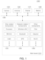
- FIG. 1 is a schematic block diagram illustrating an example of an electronic device system.
- an electronic device 1000 may accommodate a mainboard 1010 therein.
- the mainboard 1010 may include chip related components 1020 , network related components 1030 , other components 1040 , and the like, physically or electrically connected thereto. These components may be connected to other electronic components to be described below to form various signal lines 1090 .
- the chip related components 1020 may include a memory chip such as a volatile memory (for example, a dynamic random access memory (DRAM)), a non-volatile memory (for example, a read only memory (ROM)), a flash memory, or the like; an application processor chip such as a central processor (for example, a central processing unit (CPU)), a graphics processor (for example, a graphics processing unit (GPU)), a digital signal processor, a cryptographic processor, a microprocessor, a microcontroller, or the like; and a logic chip such as an analog-to-digital (ADC) converter, an application-specific integrated circuit (ASIC), or the like.
- a volatile memory for example, a dynamic random access memory (DRAM)
- ROM read only memory
- flash memory or the like
- an application processor chip such as a central processor (for example, a central processing unit (CPU)), a graphics processor (for example, a graphics processing unit (GPU)), a digital signal processor, a cryptographic
- the chip related components 1020 are not limited thereto, and may also include other types of chip related electronic components. In addition, the chip related components 1020 may be combined with each other.
- the chip-related component 1020 may be in the form of a package including the above-described chip or electronic component.
- the network related components 1030 may include protocols such as wireless fidelity (Wi-Fi) (Institute of Electrical And Electronics Engineers (IEEE) 802.11 family, or the like), worldwide interoperability for microwave access (WiMAX) (IEEE 802.16 family, or the like), IEEE 802.20, long term evolution (LTE), evolution data only (Ev-DO), high speed packet access+(HSPA+), high speed downlink packet access+(HSDPA+), high speed uplink packet access+(HSUPA+), enhanced data GSM environment (EDGE), global system for mobile communications (GSM), global positioning system (GPS), general packet radio service (GPRS), code division multiple access (CDMA), time division multiple access (TDMA), digital enhanced cordless telecommunications (DECT), Bluetooth, 3G, 4G, and 5G protocols, and any other wireless and wired protocols, designated after the abovementioned protocols.
- Wi-Fi Institutee of Electrical And Electronics Engineers (IEEE) 802.11 family, or the like
- WiMAX worldwide interoper
- Other components 1040 may include a high frequency inductor, a ferrite inductor, a power inductor, ferrite beads, a low temperature co-fired ceramic (LTCC), an electromagnetic interference (EMI) filter, a multilayer ceramic capacitor (MLCC), or the like.
- LTCC low temperature co-fired ceramic
- EMI electromagnetic interference
- MLCC multilayer ceramic capacitor
- other components 1040 are not limited thereto, and may also include passive components in the form of a chip component used for various other purposes, or the like.
- other components 1040 may be combined with each other, together with the chip related components 1020 or the network related components 1030 described above.
- the electronic device 1000 may include other electronic components that may or may not be physically or electrically connected to the mainboard 1010 .
- other electronic components include a camera module 1050 , an antenna module 1060 , a display device 1070 , a battery 1080 , and the like.
- other electronic components are not limited thereto, and may include, for example, an audio codec, a video codec, a power amplifier, a compass, an accelerometer, a gyroscope, a speaker, a mass storage unit (e.g., a hard disk drive), a compact disk (CD) drive, a digital versatile disk (DVD) drive, and the like.
- these other components may also include other electronic components used for various purposes depending on a type of electronic device 1000 , or the like.
- the electronic device 1000 may be a smartphone, a personal digital assistant (PDA), a digital video camera, a digital still camera, a network system, a computer, a monitor, a tablet PC, a laptop PC, a netbook PC, a television, a video game machine, a smartwatch, an automotive component, or the like.
- PDA personal digital assistant
- the electronic device 1000 is not limited thereto, but may be any other electronic device processing data.
- FIG. 2 is a schematic perspective view illustrating an example of an electronic device.
- the electronic device may be, for example, a smartphone 1100 .
- a motherboard 1110 is accommodated inside the smartphone 1100 , and various components 1120 are physically and/or electrically connected to the motherboard 1110 .
- other components that may or may not be physically and/or electrically connected to the motherboard 1110 , such as a camera module 1130 and/or a speaker 1140 , are accommodated in the smartphone 1100 .
- a portion of the components 1120 may be the aforementioned chip-related component, for example, the component package 1121 , but the present disclosure is not limited thereto.
- the component package 1121 may be in the form of a printed circuit board on which electronic components including active components and/or passive components are surface-mounted. Alternatively, the component package 1121 may be in the form of a printed circuit board in which active components and/or passive components are embedded.
- the electronic device is not necessarily limited to the smartphone 1100 , and may also be other electronic devices as described above.
- FIG. 3 is a cross-sectional view schematically illustrating an example of a printed circuit board.
- FIG. 4 is a schematic enlarged view according to an example of area A of FIG. 3 .
- FIG. 5 is a schematic enlarged view according to another example of area A of FIG. 3 .
- a printed circuit board 100 includes an insulating layer 110 , and a first wiring layer 120 of which at least a portion is embedded in one side of the insulating layer 110 and of which one surface is exposed from one surface of the insulating layer 110 .
- the insulating layer 110 includes a first insulating layer 111 covering at least a portion of a side surface of the first wiring layer 120 , and a second insulating layer 112 disposed on the first insulating layer 111 and the first wiring layer 120 .
- the printed circuit board 100 may further include a second wiring layer 130 disposed on the other surface of the insulating layer 110 , a via layer 140 penetrating through the insulating layer 110 and electrically connecting the first and second wiring layers 120 and 130 , a first resist layer 150 disposed on one surface of the insulating layer 110 and having a first opening 150 h exposing at least a portion of the first wiring layer 120 , and/or a second resist layer 160 disposed on the other surface of the insulating layer 110 and having a second opening 160 h exposing at least a portion of the second wiring layer 130 .
- the first and second insulating layers 111 and 112 may include different insulating materials.
- the first insulating layer 111 may include an insulating material not including a reinforcing material
- the second insulating layer 112 may include an insulating material including a reinforcing material.
- the reinforcing material is included to maintain rigidity, and may be, for example, a glass fiber (Glass Fiber, Glass Cloth, and/or Glass Fabric), but the present disclosure is not limited thereto.
- the first insulating layer 111 may include a solder resist
- the second insulating layer 112 may include a prepreg, but the present disclosure is not limited thereto.
- voids may be effectively prevented from occurring in the upper portion of the first wiring layer 120 due to a lack of a resin such as epoxy.
- an insulating material including a reinforcing material as the material of the second insulating layer 112 , even with a relatively thin thickness, sufficient rigidity may be provided to the insulating layer 110 , which may be advantageous for warpage control.
- a thickness t 1 of the first insulating layer 111 may be less than a thickness t 2 of the second insulating layer 112 .
- the thickness t 1 of the first insulating layer 111 may be thinner than a thickness t 3 of the first wiring layer 120 .
- the first insulating layer 111 may cover a portion of the side surface of the first wiring layer 120
- the second insulating layer 112 may cover another portion of the side surface of the first wiring layer 120 .
- the thickness may indicate an average thickness. The thickness may be measured by capturing an image of a cut section of the printed circuit board 100 with a scanning electron microscope, and the average thickness may be an average value of thicknesses measured at five arbitrary points.
- the first insulating layer 111 when the first insulating layer 111 is formed only sufficiently to prevent the occurrence of voids and the second insulating layer 112 is formed to a sufficient thickness, it may be more effective to simultaneously control void and warpage occurrence.
- both the first insulating layer 111 and the second insulating layer 112 may be in contact with the side surface of the first wiring layer 120 , reliability may be further improved.
- the second wiring layer 130 may include a greater number of metal layers than the first wiring layer 120 .
- the first wiring layer 120 may include only one metal layer 121 formed by electroplating
- the second wiring layer 130 may include two or more metal layers 131 and 132 , such as a metal layer 131 formed by electroless plating or with copper foil and a metal layer 132 formed by electrolytic plating.
- the via layer 140 formed together with the second wiring layer 130 may also include two or more metal layers 141 and 142 , such as a metal layer 141 formed by electroless plating or copper foil and a metal layer 142 formed by electrolytic plating.
- the metal layers 131 and 132 of the second wiring layer 130 may be integrated with the metal layers 141 and 142 of the via layer 140 , respectively.
- the printed circuit board 100 according to an example may have an ETS structure, and thus the overall thickness of the substrate may be further reduced.
- one surface of the first wiring layer 120 may be substantially coplanar with one surface of the insulating layer 110 , in detail, one surface of the first insulating layer 111 .
- being substantially coplanar may indicate that one surfaces of both are located on substantially the same level within a process error range.
- one surface of the first wiring layer 120 and one surface of the insulating layer 110 may be substantially coplanar.
- one surface of the first wiring layer 120 may have a step h with one surface of the insulating layer 110 , in detail, one surface of the first insulating layer 111 .
- having the step h may indicate that one surfaces of both the first wiring layer 120 and the insulating layer 110 are located on different levels outside the process error range.
- one surface of the first wiring layer 120 and one surface of the insulating layer 110 may have the step h.
- the first insulating layer 111 may include an insulating material.
- the insulating material may include a thermosetting resin such as an epoxy resin, or a material including an inorganic filler and/or an organic filler together with the resin.
- the insulating material may be a photosensitive material and/or a non-photosensitive material.
- Solder Resist (SR) or the like may be used as the insulating material, but the present disclosure is not limited thereto.
- SR Solder Resist
- other polymer materials that may be applied to other thinning processes may be used.
- the second insulating layer 112 may include an insulating material.
- the insulation material may include thermosetting resins such as epoxy resins, thermoplastic resins such as polyimides, or materials including inorganic fillers, organic fillers and/or glass fibers (Glass Fiber, Glass Cloth, and/or Glass Fabric) together with these resins.
- the insulating material may be a photosensitive material and/or a non-photosensitive material.
- Prepreg Prepreg
- RRCC Resin Coated Copper
- CCL Copper Clad Laminate
- the first wiring layer 120 may include a metal material.
- the metal material may include copper (Cu), aluminum (Al), silver (Ag), tin (Sn), gold (Au), nickel (Ni), lead (Pb), titanium (Ti), and/or alloys thereof.
- the first wiring layer 120 may perform various functions according to a design, and for example, may include a ground pattern, a power pattern, a signal pattern, and the like.
- the signal pattern may include a pattern providing an electrical path for various signals other than ground and power, for example, a data signal. Each of these patterns may include a line pattern, a plane pattern, and/or a pad pattern.
- the first wiring layer 120 may be an electrolytic plating layer (or electrolytic copper).
- the second wiring layer 130 may include a metal material.
- the metal material may include copper (Cu), aluminum (Al), silver (Ag), tin (Sn), gold (Au), nickel (Ni), lead (Pb), titanium (Ti), alloys thereof, and/or the like.
- the second wiring layer 130 may perform various functions according to a design, and for example, may include a ground pattern, a power pattern, a signal pattern, and the like.
- the signal pattern may include a pattern providing an electrical path for various signals other than ground and power, for example, a data signal. Each of these patterns may include a line pattern, a plane pattern, and/or a pad pattern.
- the second wiring layer 130 may include an electroless plating layer (or chemical copper) and an electrolytic plating layer (or electrolytic copper), or may include a metal foil (or copper foil) and an electrolytic plating layer (or electrolytic copper), or may include a metal foil (or copper foil), an electroless plating layer (or chemical copper), and an electrolytic plating layer (or electrolytic copper).
- the via layer 140 may include a metal material.
- the metal material may include copper (Cu), aluminum (Al), silver (Ag), tin (Sn), gold (Au), nickel (Ni), lead (Pb), titanium (Ti), alloys thereof, and/or the like.
- the via layer 140 may perform various functions according to a design, and may include a ground via, a power via, a signal via, and the like.
- the signal via may include a via for electrical connection of various signals except for ground and power, for example, a data signal or the like.
- Each of the vias of the via layer 140 may have a tapered shape in which the width of one surface connected to the first wiring layer 120 is narrower than the width of the other surface connected to the second wiring layer 130 in cross-section.
- the via layer 140 may be formed together by the same plating process as a process of the second wiring layer 130 , and thus may be integrated with the second wiring layer 130 .
- the via layer 140 may include an electroless plating layer (or chemical copper) and an electrolytic plating layer (or electrolytic copper).
- the first resist layer 150 may include an insulating material.
- the insulating material may include a thermosetting resin such as an epoxy resin, or a material including an inorganic filler and/or an organic filler together with the resin.
- the insulating material may be a photosensitive material and/or a non-photosensitive material.
- Solder Resist SR
- various polymer materials that may be used as the outermost layer material of the substrate may be used.
- the first resist layer 150 may have a plurality of openings 150 h exposing at least a portion of the first wiring layer 120 , respectively, and the opening 150 h may expose at least a portion of the first wiring layer 120 in a solder mask defined (SMD) type or a non-solder mask defined (NSMD) type, respectively.
- SMD solder mask defined
- NMD non-solder mask defined
- the second resist layer 160 may include an insulating material.
- the insulating material may include a thermosetting resin such as an epoxy resin, or a material including an inorganic filler and/or an organic filler together with the resin.
- the insulating material may be a photosensitive material and/or a non-photosensitive material.
- Solder Resist (SR) or the like may be used as the insulating material, but the present disclosure is not limited thereto.
- various polymer materials that may be used as the outermost layer material of the substrate may be used.
- the second resist layer 160 may have a plurality of openings 160 h respectively exposing at least a portion of the second wiring layer 130 , and the opening 160 h may expose at least a portion of the second wiring layer 130 in a solder mask defined (SMD) type or a non-solder mask defined (NSMD) type, respectively.
- SMD solder mask defined
- NMD non-solder mask defined
- the opening 160 h may expose at least a portion of the buildup wiring layer.
- FIGS. 6 to 14 are process diagrams schematically illustrating an example of manufacturing the printed circuit board of FIG. 3 .
- a detachable core 200 in which a metal foil 220 , for example, a copper foil is laminated on one surface or both surfaces of an insulating material 210 is prepared.
- a metal foil 220 for example, a copper foil is laminated on one surface or both surfaces of an insulating material 210
- CCL Copper Clad Laminate
- the present disclosure is not limited thereto, and in addition, various detachable cores used in the coreless process may be used.
- the first wiring layer 120 is formed on the metal foil 220 .
- the first wiring layer 120 may be formed by an electrolytic plating process using a photoresist.
- the first wiring layer 120 may be formed by forming a photoresist on the metal foil 220 and patterning the same through exposure and development processes, and then filling the patterned area with electrolytic plating and peeling the photoresist.
- a first insulating layer 111 filling the first wiring layer 120 is formed on the metal foil 220 .
- the first insulating layer 111 may be formed by, for example, applying a solder resist.
- the thickness of the first insulating layer 111 is formed thinner than the thickness of the first wiring layer 120 .
- a thinning process may be used. Therefore, the first insulating layer 111 may cover a portion of the side surface of the first wiring layer 120 , and one surface of the first wiring layer 120 may protrude upwardly of one surface of the first insulating layer 111 .
- a second insulating layer 112 is formed on the first insulating layer 111 and the first wiring layer 120 .
- the second insulating layer 112 may be formed by laminating, for example, prepreg or resin coated copper (RCC).
- the second insulating layer 112 may cover respectively the other surfaces of the first insulating layer 111 and the first wiring layer 120 , and may cover another part of the side surface of the first wiring layer 120 .
- the second wiring layer 130 and the via layer 140 are formed on the second insulating layer 112 .
- a via hole may be formed by laser processing or mechanical drilling, and after the seed layer is formed by electroless plating, the second wiring layer 130 and the via layer 140 may be formed by an electrolytic plating process using a photoresist.
- the structure manufactured by the above-described process is separated from the insulating material 210 .
- a seed layer etching process is performed.
- the metal foil 220 may be removed by the seed layer etching process. Also, the seed layer and/or the copper foil formed on the second insulating layer 112 may be removed.
- first and second resist layers 150 and 160 are formed on both surfaces of the insulating layer 110 .
- the first and second resist layers 150 and 160 may be respectively formed by applying solder resist, but the present disclosure is not limited thereto.
- first and second openings 150 h and 160 h are formed in the first and second resist layers 150 and 160 by a photolithography process or the like, respectively.
- the printed circuit board 100 according to the above-described example may be formed through a series of processes. Other overlapping contents are omitted.
- FIG. 15 is a cross-sectional view schematically illustrating another example of a printed circuit board.
- a printed circuit board 105 further includes a third insulating layer 113 disposed on the other surface of the second insulating layer 112 opposite to one surface thereof adjacent to the first insulating layer 111 and covering at least a portion of the second wiring layer 130 , a third wiring layer 135 protruding from the other surface of the third insulating layer 113 that is opposite to one surface adjacent to the second insulating layer 112 , and a second via layer 145 passing through the third insulating layer 113 and electrically connecting the second and third wiring layers 130 and 135 .
- the third insulating layer 113 may include an insulating material.
- the insulation material may include thermosetting resins such as epoxy resins, thermoplastic resins such as polyimides, or materials including inorganic fillers, organic fillers and/or glass fibers (Glass Fiber, Glass Cloth, and/or Glass Fabric) together with these resins.
- the insulating material may be a photosensitive material and/or a non-photosensitive material.
- PPG Prepreg
- RRCC Resin Coated Copper
- CCL Copper Clad Laminate
- the third insulating layer 113 may include substantially the same insulating material as the second insulating layer 112 , and substantially the same insulating material may include the case being substantially identical as well as completely identical in composition, and for example, may be an insulating layer commercially available under the same brand name or the like.
- the third wiring layer 135 may include a metal material.
- the metal material may include copper (Cu), aluminum (Al), silver (Ag), tin (Sn), gold (Au), nickel (Ni), lead (Pb), titanium (Ti), alloys thereof, and/or the like.
- the third wiring layer 135 may perform various functions according to a design, and for example, may include a ground pattern, a power pattern, a signal pattern, and the like.
- the signal pattern may include a pattern providing an electrical path for various signals other than ground and power, for example, a data signal and the like. Each of these patterns may include a line pattern, a plane pattern, and/or a pad pattern.
- the third wiring layer 135 may include an electroless plating layer (or chemical copper) and an electrolytic plating layer (or electrolytic copper), or may include a metal foil (or copper foil) and an electrolytic plating layer (or electrolytic copper), or may include a metal foil (or copper foil), an electroless plating layer (or chemical copper), and an electrolytic plating layer (or electrolytic copper).
- the second via layer 145 may include a metal material.
- the metal material may include copper (Cu), aluminum (Al), silver (Ag), tin (Sn), gold (Au), nickel (Ni), lead (Pb), titanium (Ti), alloys thereof, and/or the like.
- the second via layer 145 may perform various functions according to a design, and for example, may include a ground via, a power via, a signal via, and the like.
- the signal via may include a via for electrical connection of various signals except for ground and power, for example, a data signal and the like.
- the via of the second via layer 145 may have a tapered shape in which the width of one surface connected to the second wiring layer 130 is narrower than the width of the other surface connected to the third wiring layer 135 , on a cross-section.
- the second via layer 145 may be formed together by the same plating process as the third wiring layer 135 , and thus may be integrated with the third wiring layer 135 .
- the second via layer 145 may include an electroless plating layer (or chemical copper) and an electrolytic plating layer (or electrolytic copper).
- a fourth insulating layer may be further disposed between the second insulating layer 112 and the third insulating layer 113 , and in this case, the second wiring layer 130 may be embedded in one surface of the fourth insulating layer in such a manner that one surface is exposed from the one surface of the fourth insulating layer.
- the second via layer 145 may also pass through the fourth insulating layer.
- the fourth insulating layer may be thinner than each of the second wiring layer 130 and the third insulating layer 113 . Accordingly, the fourth insulating layer may cover a portion of the side surface of the second wiring layer 130 , and the third insulating layer 113 may cover the remaining part of the side surface of the second wiring layer 130 .
- the fourth insulating layer may include substantially the same insulating material as the first insulating layer 111 . In addition, the characteristics described for the other first insulating layer 111 may also be applied to the fourth insulating layer.
- a build-up insulating layer, a build-up wiring layer, and a build-up via layer may be further formed on the other surface of the insulating layer 110 , and the specific number of layers is not specifically limited.
- the build-up insulating layer may respectively include a plurality of insulating layers such as the first and second insulating layers 111 and 112 , like the insulating layer 110 , or only one insulating layer such as the second insulating layer 112 .
- Each of the build-up wiring layers may include substantially the same structure and material as that of the second wiring layer 130 .
- Each of the build-up via layers may include substantially the same structure and material as the via layer 140 .
- a substrate having an ETS structure capable of preventing void defects even when a relatively thin material including glass is used may be provided.
- ‘on the cross-section’ may indicate a cross-sectional shape when the object is vertically cut, or a cross-sectional shape when the object is viewed from a side-view.
- the meaning on a plane may be a shape when the object is horizontally cut, or a flat shape when the object is viewed from a top-view or a bottom-view.
- the lower side, the lower portion, the lower surface, and the like are used to refer to the direction toward the mounting surface of the semiconductor package including the organic interposer based on the cross section of the drawing for convenience, and the upper side, upper portion, upper surface and the like are used in the direction opposite thereto.
- this is to define the direction for convenience of explanation, and the scope of the claims is not limited by the description in this direction.
- the meaning of being connected in the present disclosure is a concept including not only directly connected, but also indirectly connected through an adhesive layer or the like.
- the meaning of being electrically connected is a concept including both the case of being physically connected and the case of not being connected.
- expressions such as first, second, and the like are used to distinguish one component from another, and do not limit the order and/or importance of the corresponding components.
- the first component may be named as the second component, and similarly, the second component may be named as the first component.
- an example used in the present disclosure does not mean the same embodiment, and is provided to emphasize and explain different unique features.
- the examples presented above are not excluded from being implemented in combination with features of other examples. For example, even if a matter described in one specific example is not described in another example, it may be understood as a description related to another example unless a description contradicts the matter in another example.
Landscapes
- Engineering & Computer Science (AREA)
- Microelectronics & Electronic Packaging (AREA)
- Manufacturing & Machinery (AREA)
- Chemical & Material Sciences (AREA)
- Ceramic Engineering (AREA)
- Inorganic Chemistry (AREA)
- Production Of Multi-Layered Print Wiring Board (AREA)
Abstract
Description
Claims (20)
Applications Claiming Priority (2)
| Application Number | Priority Date | Filing Date | Title |
|---|---|---|---|
| KR10-2022-0068861 | 2022-06-07 | ||
| KR1020220068861A KR20230168426A (en) | 2022-06-07 | 2022-06-07 | Printed circuit board |
Publications (2)
| Publication Number | Publication Date |
|---|---|
| US20230397330A1 US20230397330A1 (en) | 2023-12-07 |
| US12156329B2 true US12156329B2 (en) | 2024-11-26 |
Family
ID=88976331
Family Applications (1)
| Application Number | Title | Priority Date | Filing Date |
|---|---|---|---|
| US17/901,402 Active 2043-04-07 US12156329B2 (en) | 2022-06-07 | 2022-09-01 | Printed circuit board |
Country Status (4)
| Country | Link |
|---|---|
| US (1) | US12156329B2 (en) |
| JP (1) | JP2023179343A (en) |
| KR (1) | KR20230168426A (en) |
| CN (1) | CN117202475A (en) |
Families Citing this family (1)
| Publication number | Priority date | Publication date | Assignee | Title |
|---|---|---|---|---|
| KR20240067555A (en) | 2022-11-09 | 2024-05-17 | 삼성전기주식회사 | Printed circuit board |
Citations (3)
| Publication number | Priority date | Publication date | Assignee | Title |
|---|---|---|---|---|
| US20160021744A1 (en) | 2014-07-21 | 2016-01-21 | Samsung Electro-Mechanics Co., Ltd. | Printed circuit board and method of manufacturing the same |
| US20160234932A1 (en) * | 2015-02-10 | 2016-08-11 | Shinko Electric Industries Co., Ltd. | Circuit board and method of manufacturing circuit board |
| US20210282277A1 (en) | 2018-06-08 | 2021-09-09 | Unimicron Technology Corp. | Manufacturing method of circuit carrier board |
-
2022
- 2022-06-07 KR KR1020220068861A patent/KR20230168426A/en active Pending
- 2022-09-01 US US17/901,402 patent/US12156329B2/en active Active
- 2022-09-07 JP JP2022142098A patent/JP2023179343A/en active Pending
- 2022-11-14 CN CN202211424053.7A patent/CN117202475A/en active Pending
Patent Citations (4)
| Publication number | Priority date | Publication date | Assignee | Title |
|---|---|---|---|---|
| US20160021744A1 (en) | 2014-07-21 | 2016-01-21 | Samsung Electro-Mechanics Co., Ltd. | Printed circuit board and method of manufacturing the same |
| KR20160010960A (en) | 2014-07-21 | 2016-01-29 | 삼성전기주식회사 | Printed circuit board and manufacturing method thereof |
| US20160234932A1 (en) * | 2015-02-10 | 2016-08-11 | Shinko Electric Industries Co., Ltd. | Circuit board and method of manufacturing circuit board |
| US20210282277A1 (en) | 2018-06-08 | 2021-09-09 | Unimicron Technology Corp. | Manufacturing method of circuit carrier board |
Also Published As
| Publication number | Publication date |
|---|---|
| US20230397330A1 (en) | 2023-12-07 |
| JP2023179343A (en) | 2023-12-19 |
| KR20230168426A (en) | 2023-12-14 |
| CN117202475A (en) | 2023-12-08 |
Similar Documents
| Publication | Publication Date | Title |
|---|---|---|
| US20240215157A1 (en) | Printed circuit board | |
| US12224235B2 (en) | Printed circuit board | |
| US12156329B2 (en) | Printed circuit board | |
| US20230199974A1 (en) | Printed circuit board and method for manufacturing the same | |
| US12133329B2 (en) | Printed circuit board and method for manufacturing the same | |
| US12022613B2 (en) | Printed circuit board | |
| US11895771B2 (en) | Printed circuit board | |
| US11627659B2 (en) | Printed circuit board and electronic package comprising the same | |
| US11882652B2 (en) | Printed circuit board | |
| US11758653B2 (en) | Printed circuit board | |
| US12349273B2 (en) | Printed circuit board | |
| US12526919B2 (en) | Printed circuit board | |
| US12004296B2 (en) | Printed circuit board | |
| US12256492B2 (en) | Printed circuit board | |
| US20230413437A1 (en) | Printed circuit board | |
| US20250126710A1 (en) | Printed circuit board | |
| US12022621B2 (en) | Printed circuit board and method for manufacturing the same | |
| US20240431023A1 (en) | Printed circuit board | |
| US11715680B2 (en) | Printed circuit board | |
| US20240164013A1 (en) | Printed circuit board and manufacturing method for the same | |
| KR102827660B1 (en) | Printed circuit board | |
| JP2025100405A (en) | Printed Circuit Board |
Legal Events
| Date | Code | Title | Description |
|---|---|---|---|
| FEPP | Fee payment procedure |
Free format text: ENTITY STATUS SET TO UNDISCOUNTED (ORIGINAL EVENT CODE: BIG.); ENTITY STATUS OF PATENT OWNER: LARGE ENTITY |
|
| AS | Assignment |
Owner name: SAMSUNG ELECTRO-MECHANICS CO., LTD., KOREA, REPUBLIC OF Free format text: ASSIGNMENT OF ASSIGNORS INTEREST;ASSIGNORS:CHOI, SEONG HO;JEON, SEONG IL;REEL/FRAME:061373/0927 Effective date: 20220822 |
|
| STPP | Information on status: patent application and granting procedure in general |
Free format text: DOCKETED NEW CASE - READY FOR EXAMINATION |
|
| STPP | Information on status: patent application and granting procedure in general |
Free format text: NON FINAL ACTION MAILED |
|
| STPP | Information on status: patent application and granting procedure in general |
Free format text: RESPONSE TO NON-FINAL OFFICE ACTION ENTERED AND FORWARDED TO EXAMINER |
|
| STPP | Information on status: patent application and granting procedure in general |
Free format text: NOTICE OF ALLOWANCE MAILED -- APPLICATION RECEIVED IN OFFICE OF PUBLICATIONS |
|
| STPP | Information on status: patent application and granting procedure in general |
Free format text: PUBLICATIONS -- ISSUE FEE PAYMENT RECEIVED |
|
| STCF | Information on status: patent grant |
Free format text: PATENTED CASE |