US12155751B2 - Processor with block cipher algorithm, and a data encryption and decryption method operated by the processor - Google Patents
Processor with block cipher algorithm, and a data encryption and decryption method operated by the processor Download PDFInfo
- Publication number
- US12155751B2 US12155751B2 US17/837,674 US202217837674A US12155751B2 US 12155751 B2 US12155751 B2 US 12155751B2 US 202217837674 A US202217837674 A US 202217837674A US 12155751 B2 US12155751 B2 US 12155751B2
- Authority
- US
- United States
- Prior art keywords
- input
- processor
- block
- hardware
- keys
- Prior art date
- Legal status (The legal status is an assumption and is not a legal conclusion. Google has not performed a legal analysis and makes no representation as to the accuracy of the status listed.)
- Active, expires
Links
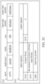
Images


Classifications
-
- G—PHYSICS
- G06—COMPUTING OR CALCULATING; COUNTING
- G06F—ELECTRIC DIGITAL DATA PROCESSING
- G06F21/00—Security arrangements for protecting computers, components thereof, programs or data against unauthorised activity
- G06F21/30—Authentication, i.e. establishing the identity or authorisation of security principals
- G06F21/45—Structures or tools for the administration of authentication
- G06F21/46—Structures or tools for the administration of authentication by designing passwords or checking the strength of passwords
-
- H—ELECTRICITY
- H04—ELECTRIC COMMUNICATION TECHNIQUE
- H04L—TRANSMISSION OF DIGITAL INFORMATION, e.g. TELEGRAPHIC COMMUNICATION
- H04L9/00—Cryptographic mechanisms or cryptographic arrangements for secret or secure communications; Network security protocols
- H04L9/08—Key distribution or management, e.g. generation, sharing or updating, of cryptographic keys or passwords
- H04L9/0816—Key establishment, i.e. cryptographic processes or cryptographic protocols whereby a shared secret becomes available to two or more parties, for subsequent use
- H04L9/0819—Key transport or distribution, i.e. key establishment techniques where one party creates or otherwise obtains a secret value, and securely transfers it to the other(s)
- H04L9/0825—Key transport or distribution, i.e. key establishment techniques where one party creates or otherwise obtains a secret value, and securely transfers it to the other(s) using asymmetric-key encryption or public key infrastructure [PKI], e.g. key signature or public key certificates
-
- G—PHYSICS
- G06—COMPUTING OR CALCULATING; COUNTING
- G06F—ELECTRIC DIGITAL DATA PROCESSING
- G06F21/00—Security arrangements for protecting computers, components thereof, programs or data against unauthorised activity
- G06F21/60—Protecting data
- G06F21/602—Providing cryptographic facilities or services
-
- H—ELECTRICITY
- H04—ELECTRIC COMMUNICATION TECHNIQUE
- H04L—TRANSMISSION OF DIGITAL INFORMATION, e.g. TELEGRAPHIC COMMUNICATION
- H04L9/00—Cryptographic mechanisms or cryptographic arrangements for secret or secure communications; Network security protocols
- H04L9/002—Countermeasures against attacks on cryptographic mechanisms
-
- H—ELECTRICITY
- H04—ELECTRIC COMMUNICATION TECHNIQUE
- H04L—TRANSMISSION OF DIGITAL INFORMATION, e.g. TELEGRAPHIC COMMUNICATION
- H04L9/00—Cryptographic mechanisms or cryptographic arrangements for secret or secure communications; Network security protocols
- H04L9/06—Cryptographic mechanisms or cryptographic arrangements for secret or secure communications; Network security protocols the encryption apparatus using shift registers or memories for block-wise or stream coding, e.g. DES systems or RC4; Hash functions; Pseudorandom sequence generators
- H04L9/0618—Block ciphers, i.e. encrypting groups of characters of a plain text message using fixed encryption transformation
-
- H—ELECTRICITY
- H04—ELECTRIC COMMUNICATION TECHNIQUE
- H04L—TRANSMISSION OF DIGITAL INFORMATION, e.g. TELEGRAPHIC COMMUNICATION
- H04L9/00—Cryptographic mechanisms or cryptographic arrangements for secret or secure communications; Network security protocols
- H04L9/08—Key distribution or management, e.g. generation, sharing or updating, of cryptographic keys or passwords
- H04L9/0861—Generation of secret information including derivation or calculation of cryptographic keys or passwords
- H04L9/0866—Generation of secret information including derivation or calculation of cryptographic keys or passwords involving user or device identifiers, e.g. serial number, physical or biometrical information, DNA, hand-signature or measurable physical characteristics
-
- H—ELECTRICITY
- H04—ELECTRIC COMMUNICATION TECHNIQUE
- H04L—TRANSMISSION OF DIGITAL INFORMATION, e.g. TELEGRAPHIC COMMUNICATION
- H04L2209/00—Additional information or applications relating to cryptographic mechanisms or cryptographic arrangements for secret or secure communication H04L9/00
- H04L2209/80—Wireless
Definitions
- the present application relates to a processor with a cryptographic algorithm and a data encryption and decryption method.
- SM2, SM3, SM4 and other cryptographic algorithms, replacing RSA (abbreviated from Rivest-Shamir-Adleman), SHA (abbreviated from Secure Hash Algorithm), AES (Advanced Encryption Standard), and other international general cryptographic algorithms.
- RSA abbreviated from Rivest-Shamir-Adleman
- SHA abbreviated from Secure Hash Algorithm
- AES Advanced Encryption Standard
- SM4 is a block cipher algorithm, which is applied to wireless local area network products.
- the data block length and the key length of SM4 are both 128 bits.
- ISA instruction set architecture
- a high-security processor with a block cipher algorithm (SM4) and a high security data encryption and decryption method for the block cipher algorithm (SM4) are presented.
- a processor in accordance with an exemplary embodiment of the present application uses a first register to store an input key pointer, pointing to an input key.
- the processor reads input data from a first system memory area, performs the block cipher algorithm on the input data based on the input key to encrypt or decrypt the input data to generate output data, and stores the output data in a second system memory area, or an internal storage area within the processor.
- a data encryption and decryption method operated by a processor in accordance with an exemplary embodiment comprising: in response to one single block cipher instruction, reading input data from a first system memory area, performing a block cipher algorithm on the input data based on an input key to encrypt or decrypt the input data to generate output data, and storing the output data in a second system memory area or an internal storage area within the processor.
- FIG. 1 is a block diagram illustrating a processor 100 in accordance with an exemplary embodiment of the present application
- FIGS. 2 A to 2 C show examples regarding the instruction format of the ISA SM4 instruction, and further show the related design about the microcode UCODE;
- FIG. 3 illustrates the programming of ISA instructions in accordance with an exemplary embodiment of the present application
- FIG. 4 is a flow chart, illustrating a procedure called by the SM4 algorithm in accordance with an exemplary embodiment of the present application
- FIG. 5 illustrates an SM4 engine 500 in accordance with an exemplary embodiment of the present application.
- the present application discloses a processor with a block cipher algorithm (SM4 algorithm), and proposes a block cipher instruction (SM4 instruction) that is an Instruction Set Architecture (ISA) instruction.
- the microcode (UCODE) of the processor is specially designed for the SM4 instruction, and there is a block cipher algorithm accelerator (SM4 engine) in an encryption and decryption unit of the processor.
- the processor decodes the SM4 instruction to microinstructions according to the microcode. According to the microinstructions, the contents in the architectural registers are interpreted and used in operating the SM4 engine to implement the SM4 algorithm.
- the instruction set supported by the processor may include an x86 instruction set.
- the intermediate data generated during the SM4 algorithm (for example, the extended keys, or the intermediate calculation data generated before getting the output data based on the input data) can be safely hidden in the internal storage space within the processor.
- FIG. 1 is a block diagram illustrating a processor 100 in accordance with an exemplary embodiment of the present application.
- a branch predictor 102 instructions are loaded into the instruction cache 104 by checking an instruction translation lookaside buffer (ITLB), and then buffered in an instruction buffer (XIB) 106 , and then pushed into a format instruction queue (FIQ) 108 waiting to be decoded by the decoder 110 .
- ILB instruction translation lookaside buffer
- XIB instruction buffer
- FIQ format instruction queue
- the microinstructions are pushed into an instruction queue (XIQ) 112 , and then are issued into the corresponding reservation stations RS via a rename unit 114 , to drive the arithmetic logical unit ALU, address generating units AGU of a memory order buffer (MOB) 116 , hardware Fadd, Fmul, Fmisc, and MMX, or an encryption and decryption unit 118 .
- the data required in calculations may be loaded into a data cache 120 by checking a data translation lookaside buffer DTLB, and then stored in the memory order buffer (MOB) 116 .
- the processor 100 further includes a reorder buffer (ROB) 122 , and architectural registers 124 required in the operations.
- ROB reorder buffer
- the encryption and decryption unit 118 includes an SM4 engine 126 .
- SM4 engine 126 there are microinstructions about accessing the architectural registers 124 in response to the SM4 instruction. For example, there are microinstructions operative to read a register storing a control word (that shows whether to perform encryption or decryption, and shows operating the SM4 algorithm in what mode), to read a register recording the amount of 16-byte input blocks carried in the input data, to read a register recording an input key pointer, or even to read a register storing information about the input and output data.
- a control word that shows whether to perform encryption or decryption, and shows operating the SM4 algorithm in what mode
- the decoder 110 decodes the SM4 instruction (which is an ISA instruction) into a plurality of microinstructions that can be recognized by the pipelined hardware of the processor 100 , and interprets the contents of the architecture registers 124 to obtain the control word, input key. According to the microinstructions, the control word, the input key, and the input data are read from the architectural registers 124 to drive the SM4 engine 126 . Based on the input key, the SM4 engine 126 encrypts or decrypts the input data according to the SM4 algorithm, and generates the output data.
- the SM4 engine 126 Based on the input key, the SM4 engine 126 encrypts or decrypts the input data according to the SM4 algorithm, and generates the output data.
- the output data may be written into a system memory (e.g., a random access memory RAM, which may follow the ES segmentation technology), or be written into an internal storage area (e.g., a storage space within the processor 100 ).
- the decoded microinstructions include an engine driving microinstruction (an SM4 engine microinstruction), which is operative to drive the SM4 engine 126 .
- the decoded microinstructions are operative to read and update the architectural registers 124 , and operate the encryption and decryption unit 118 to perform the SM4 algorithm on the input data based on the input key.
- FIGS. 2 A to 2 C show examples regarding the instruction format of the ISA SM4 instruction, and further show the related design about the microcode UCODE.
- FIG. 2 A illustrates an instruction format 202 of the ISA SM4 instruction, and presents a table 204 to introduce the related design in the microcode UCODE.
- the prefix, opcode, and ModR/M fields presented in the instruction format 202 are filled: 0xF3 0x0F 0xA7 0xF0.
- the SIB, Displacement, and Immediate fields are not filled (non).
- the decoder 110 decodes the ISA SM4 instruction, based on the microcode UCODE, into a plurality of microinstructions.
- the contents in the architectural registers 124 are defined, read and updated.
- the encryption and decryption unit 118 including the SM4 engine 126 is operated to perform the SM4 algorithm on input data based on an input key.
- the input registers include the EBX register (the first register), the ECX register (the second register), the EAX register (the third register), the ESI register (the fourth register), and the EDI register (the fifth register) in the architectural registers 124 .
- the third register EAX stores a control word, which includes a plurality of bits.
- Bit[0] of the control word is an encryption and decryption setting bit, and it indicates an encryption operation by “0”, and indicates a decryption operation by “1”.
- Bit[10:6] of the control word indicates the SM4 mode, where “1” refers to an electronic code book (ECB) mode, “2” refers to a cipher block chaining (CBC) mode, “4” refers to a cipher feedback (CFB) mode, “8” refers to an output feedback (OFB) mode, and “10” refers to a counter (CTR) mode.
- the second register ECX stores the amount of 16-byte (128 bits) input blocks carried in the input data.
- the first register EBX stores an input key pointer pointing to a system memory area storing an input key, which may follow the ES segmentation technology.
- the fourth register ESI stores an input data pointer pointing to another system memory area that stores input data, which may follow the ES segmentation technology.
- the control word indicates an encryption operation
- the input data pointer stored in ESI register points to a section of plaintext.
- the control word indicates a decryption operation
- the input data pointer stored in ESI register points to a section of ciphertext.
- the fifth register EDI stores an output data pointer indicating where to store the output data, which may follow the ES segmentation technology.
- the output data pointer stored in EDI register points to a system memory area for storage of a section of ciphertext.
- the output data pointer stored in EDI register points to a system memory area for storage of a section of plaintext.
- Table 204 further shows what architectural registers are defined as output registers in the microcode UCODE corresponding to the SM4 instruction.
- the second register ECX is cleared to 0.
- the input data pointer in the fourth register ESI and the output data pointer in the fifth register EDI are increased. After performing the SM4 algorithm on the whole input data, the displacement increased on the value stored in the fourth register ESI reaches the byte number of the input data, and the displacement increased on the value stored in the fifth register EDI reaches the byte number of the output data.
- input and output registers may have the other design, depending on the user's requirements.
- FIG. 2 B illustrates another instruction format 212 of the ISA SM4 instruction, and presents a table 214 to introduce the related design in the microcode UCODE.
- the instruction format 212 is the same as the instruction format 202 .
- the decoder 110 decodes the ISA SM4 instruction, based on the microcode UCODE, into a plurality of microinstructions.
- the contents in the architectural registers 124 are defined, read and updated and, based on the contents in the architectural registers 124 , the encryption and decryption unit 118 including the SM4 engine 126 is operated to perform the SM4 algorithm on the input data based on an input key.
- the code for recognizing the instruction format 212 is different from the code “0xF3 0x0F 0xA7 0xF0” representing the instruction format 202 . In this way, the processor may execute various SM4 instructions with different instruction formats.
- Table 214 shows that according to the design of the microcode UCODE the fourth register ESI stores an input and output information pointer.
- the input and output information pointer points to a system memory area storing an input data pointer pointing to the input data stored in the system memory and an output data pointer pointing to the output data stored in the system memory.
- the contents in the fourth register ESI are not changed by the microcode UCODE when the SM4 algorithm is finished.
- FIG. 2 C illustrates another instruction format 222 of the ISA SM4 instruction, and presents a table 224 to introduce the related design in the microcode UCODE.
- the instruction format 212 further provides two fields InPointer and OutPointer storing an input data pointer and output data pointer, respectively.
- the input data pointer points to input data stored in the system memory.
- the output data pointer indicates a storage space in the system memory for storage of the output data.
- the decoder 110 decodes the ISA SM4 instruction, based on the microcode UCODE, into a plurality of microinstructions.
- the contents in the architectural registers 124 are defined (referring to table 224 ), read and updated.
- the encryption and decryption unit 118 including the SM4 engine 126 is operated to perform SM4 algorithm on the input data according to an input key.
- the two fields InPointer and OutPointer each are 32 bits.
- FIG. 3 illustrates the programming of ISA instructions in accordance with an exemplary embodiment of the present application.
- the program code 300 there may include an SM4 instruction 302 in the above format 202 , 212 , or 222 , and may further include register setting instruction(s) 304 prior to the SM4 instruction 302 .
- the register setting instruction(s) 304 the architectural registers 124 are filled to contain the information required during the execution of the SM4 instruction 304 .
- FIG. 4 is a flow chart, illustrating a procedure of the SM4 algorithm in accordance with an exemplary embodiment of the present application. The illustrated steps may correspond to the microinstructions decoded from the ISA SM4 instruction.
- Step S 402 checks the number of input blocks carried in the input data (for example, reading the second register ECX). If the number of input blocks is 0 (ECX is 0), step S 404 is performed to end the SM4 algorithm. If the block number is not 0 (ECX is not 0), step S 406 is performed to operate the SM4 engine 126 according to a control word, an input key, and one input data block (decomposed from the input data). In step S 408 , an output block generated by the SM4 engine 126 is programmed into the system memory to form the output data. Then, the SM4 engine 126 subtracts 1 from the value in the second register ECX. Step S 410 checks whether the SM4 algorithm on all input blocks is completed.
- step S 406 For example, check whether the second register ECX is 0. If ECX is non-zero, the procedure returns to step S 406 to operate the SM4 engine 126 according to the control word, the input key, and the next input block. If ECX is 0, the flow proceeds to step S 412 to end the SM4 algorithm. In another exemplary embodiment, the step that the SM4 engine 126 performs to subtract 1 from the value in the second register ECX is arranged after step S 406 and prior to step S 408 .
- the engine driving microinstruction corresponds to the step S 406 that operates the SM4 engine 126 to complete the SM4 algorithm on each input block.
- FIG. 5 illustrates an SM4 engine 500 in accordance with an exemplary embodiment of the present application, including hardware for implementing a control logic 502 , a routine logic 504 , a key extension logic 506 , and an anti-tone transform 508 .
- the SM4 engine 500 further provides internal storage spaces M1 ⁇ M3 and a multiplexer MUX.
- an input key 510 is read from the system memory and entered the SM4 engine 500 .
- the key extension logic 506 Based on the input key 510 , the key extension logic 506 generates 32 keys rk 0 . . . rk 31 required in the 32 rounds of calculation of each input block, and stores the 32 keys rk 0 . . . rk 31 in the internal storage space M1 within the SM4 engine 500 as the 32 sequential keys.
- the anti-tone transform 508 reverses the order of the 32 sequential keys rk 0 . . . rk 31 , and stores the 32 reversed-order keys rk 31 . . .
- the 32 sequential keys rk 0 . . . rk 31 as well as the 32 reversed-order keys rk 31 . . . rk 0 are sent to the multiplexer MUX.
- the control word 512 is read from the third register EAX. According to the control word 512 , the control logic 502 provides a selection signal dec/enc to switch the multiplexer MUX between encryption and decryption. Depending on the selection signal dec/enc, the routine logic 504 receives the sequential keys rk 0 . . . rk 31 for encryption, or the reversed-order keys rk 31 . . . rk 0 for decryption.
- the input data 514 is read from the system memory, and is entered to the routine logic 504 block by block.
- the routine logic 504 uses the 32 keys received from the multiplexer MUX to perform 32 rounds of calculation for encryption or 32 rounds of calculation for decryption on each input block.
- the routine logic 504 includes a multi-XOR logic 516 , a non-linear transform 518 , a linear transform 520 , a single XOR logic 522 , and an anti-tone transform 524 .
- the same hardware is used in encryption and decryption.
- the internal hardware design is as follows.
- Key extension logic 506 includes hardware for a key-XOR logic 526 , a multi-XOR logic 528 , a non-linear transform 530 , a linear transform 532 , and a single XOR logic 534 .
- the system parameter FK and the fixed parameter CK can be read from the internal storage space M3.
- the internal hardware design of the key extension logic 506 is as follows.
- extension keys rk i (in the sequential order or in the reversed order) are safely protected within the SM4 engine 500 . Even the routine logic 504 and the key extension logic 506 safely protect the intermediate data of the rounding calculations and the key extension calculations in the SM4 engine 500 . In such a design, a higher security hardware is provided for performing the SM4 cipher algorithm.
- the processor performs N rounds of calculation on each input block to transform each input block into an output block, and the output blocks corresponding to the different input blocks are combined to form the output data, where N is an integer.
- the processor generates N extension keys based on an input key, so that for each input block different extension keys are adopted in the different rounds of calculation.
- N is not limited to 32.
- the encryption and decryption unit 118 does not include the specifically designed SM4 engine 126 .
- the microcode UCODE is specially designed to transform an ISA SM4 instruction into a plurality of microinstructions to operate the
- the intermediate data generated during the calculations of the SM4 algorithm is safely protected within the internal storage space of the processor, too.
- the SM4 engine is not as powerful as the foregoing SM4 engine 500 .
- Some functional modules of the SM4 engine 500 (for example, the key extension logic 506 ) are implemented by the existing arithmetic logic units ALUs which are operated by microinstructions generated according to a specially designed microcode UCODE. This embodiment can also protect important intermediate data of the SM4 algorithm in the internal storage space of the processor.
- a processor in accordance with an exemplary embodiment of the present application includes an encryption and decryption unit, a set of architectural registers, a microcode storage device storing microcode, and a decoder.
- a block cipher instruction e.g., an SM4 instruction
- the decoder In response to a block cipher instruction (e.g., an SM4 instruction) of an instruction set architecture (ISA), the decoder generates, based on the microcode, a plurality of microinstructions.
- the microinstructions the architectural registers are defined, accessed and managed.
- the plurality of microinstructions operate the encryption and decryption unit to perform a block cipher algorithm (SM4 algorithm) to transform input data into output data based on an input key.
- SM4 algorithm block cipher algorithm
- Extension keys originated from the input key for performing the block cipher algorithm on the input data are protected in the internal storage space within the processor, thereby greatly improving the data security.
Landscapes
- Engineering & Computer Science (AREA)
- Computer Security & Cryptography (AREA)
- Computer Networks & Wireless Communication (AREA)
- Signal Processing (AREA)
- Theoretical Computer Science (AREA)
- Physics & Mathematics (AREA)
- Computer Hardware Design (AREA)
- Software Systems (AREA)
- General Engineering & Computer Science (AREA)
- General Physics & Mathematics (AREA)
- General Health & Medical Sciences (AREA)
- Bioethics (AREA)
- Health & Medical Sciences (AREA)
- Storage Device Security (AREA)
Abstract
Description
-
- The
multi-XOR logic 516 performs the following calculations:
(X i+1 ∧X i+2 ∧X i+3 ∧k i) - where ‘∧’ refers to a 32-bit exclusive OR calculation.
- The
non-linear transform 518 performs the following calculations: - B=t(A),
- which is (b0, b1, b2, b3)=(Sbox(a0), Sbox(a1), Sbox(a2), Sbox(a3)),
- where:
- ‘Sbox’ refers to an S-box operation, which is a fixed swap between 8-bit input and 8-bit output;
- ‘A’ is the input of the
hardware block 518, A=(a0, a1, a2, a3)∈(Z2 8)4. - ‘B’ is the output of the
hardware block 518, B=(b0, b1, b2, b3)∈(Z2 8)4. - The
linear transform 520 performs the following calculations:
L(B)=B∧(B<<<2)∧(B<<<10)∧(B<<<18)∧(B<<<24) - where ‘<<<i’ refers to a cyclic left shift of i bits, which is performed on 32-bit data.
- The
single XOR logic 522 performs the following calculations:
X i+4 −X i ∧T(X i+1 ∧X i+2 ∧X i+3 ∧k i) - where “T” refers to a reversible transform, T(Xi+1∧Xi+2∧Xi+3∧ki) is the calculation result of the
nonlinear transform 518 and thelinear transform 520, and T(.)=L (t(.)). - The
anti-tone transform 524 performs the following calculations:
R(A 0 ,A 1 ,A 2 ,A 3)=(A 3 ,A 2 ,A 1 ,A 0) - A is the input of the
hardware block 524. After 32 rounds of calculation, the anti-tone transform 524 outputs an output block (Y0, Y1, Y2, Y3)∈(Z2 32)4 corresponding to the target input block (X0, X1, X2, X3), and the output block (Y0, Y1, Y2, Y3) is R(X32, X33, X34, X35), which 1S (X35, X34, X33, X32).
- The
-
- The key-XOR logic 526 performs the following calculations:
- (K0, K1, K2, K3)=(MK0∧FK0, MK1∧FK1, MK2∧FK2, MK3∧FK3)
- where “∧” refers to a 32-bit exclusive OR calculation.
- The
multi-XOR logic 528 performs the following calculations:
(K i+1 ∧K i+2 ∧K i+3 ∧CK i) - The non-linear transform 530 performs the following calculations:
B=t(A),that is(b 0 ,b 1 ,b 2 ,b 3)=(Sbox(a 0),Sbox(a 1),Sbox(a 2),Sbox(a 3)), - where:
- Sbox refers to an S-box operation, which is a fixed swap between 8-bit input and 8-bit output;
- ‘A’ is the input of the hardware block 530, and A=(a0, a1, a2, a3)∈(Z2 8)4.
- ‘B’ is the output of the hardware block 530, and B=(b0, b1, b2, b3)∈(Z2 8)4.
- The
linear transform 532 performs the following calculations:
L′(B)=B∧(B<<<13)∧(B<<<23) - where ‘<<<i’ refers to a cyclic left shift of i bits, which is performed on 32-bit data.
- The single XOR logic 534 performs the following calculations:
rk i =K i+4 =K i ∧T′(K i+1 ∧X i+2 ∧X i+3 ∧CK i) - where T′ is a reversible conversion, T′(Ki+1∧Xi+2∧Xi+3″CKi) is the calculation result of the nonlinear conversion 530 and the
linear conversion 532, and T′(.)=L′(t(.)). rki, i=0, . . . , 31 are calculated in sequence and stored in the internal storage space M1 within theSM4 engine 500, and theanti-tone transform 508 performs a reverse order conversion to form the reversed-order keys and stores them in the internal storage space M2 within theSM4 engine 500.
Claims (28)
(K0, K1, K2, K3)=(MK0∧FK0, MK1∧FK1, MK2∧FK2, MK3∧FK3)
(Ki+1∧Ki+2∧Ki+3∧CKi);
rki=Ki+4=KiT′ (Ki+1∧Xi+2∧Xi+3∧CKi),
L(B)=B∧(B<<<2)∧(B<<<10)∧(B<<<18)∧(B<<<24);
Applications Claiming Priority (3)
| Application Number | Priority Date | Filing Date | Title |
|---|---|---|---|
| CN202111019625.9 | 2021-09-01 | ||
| CN202111019625 | 2021-09-01 | ||
| CN202111019625.9A CN113722702B (en) | 2021-09-01 | 2021-09-01 | Processor with block cipher algorithm and processing method thereof |
Publications (2)
| Publication Number | Publication Date |
|---|---|
| US20230067896A1 US20230067896A1 (en) | 2023-03-02 |
| US12155751B2 true US12155751B2 (en) | 2024-11-26 |
Family
ID=78680403
Family Applications (1)
| Application Number | Title | Priority Date | Filing Date |
|---|---|---|---|
| US17/837,674 Active 2043-01-19 US12155751B2 (en) | 2021-09-01 | 2022-06-10 | Processor with block cipher algorithm, and a data encryption and decryption method operated by the processor |
Country Status (2)
| Country | Link |
|---|---|
| US (1) | US12155751B2 (en) |
| CN (1) | CN113722702B (en) |
Families Citing this family (5)
| Publication number | Priority date | Publication date | Assignee | Title |
|---|---|---|---|---|
| CN114244510B (en) * | 2021-12-20 | 2024-08-06 | 深圳忆联信息系统有限公司 | Hardware acceleration device, method, equipment and storage medium |
| CN115549911B (en) * | 2022-11-28 | 2023-03-14 | 苏州浪潮智能科技有限公司 | Encryption and decryption system, method, processor and server |
| US12086596B2 (en) * | 2023-02-06 | 2024-09-10 | Intel Corporation | Instructions for accelerating Keccak execution in a processor |
| CN116204911B (en) * | 2023-04-27 | 2023-08-04 | 苏州浪潮智能科技有限公司 | Encryption and decryption system, encryption and decryption control method, computer device and storage medium |
| CN119989430B (en) * | 2025-01-20 | 2025-10-10 | 杭州电子科技大学 | An encryption and decryption circuit system and method based on RISC-V architecture |
Citations (15)
| Publication number | Priority date | Publication date | Assignee | Title |
|---|---|---|---|---|
| US20080292100A1 (en) * | 2007-05-24 | 2008-11-27 | Kabushiki Kaisha Toshiba | Non-linear data converter, encoder and decoder |
| US20100107249A1 (en) | 2008-10-27 | 2010-04-29 | Advanced Micro Devices, Inc. | Method, Apparatus, and Device for Protecting Against Programming Attacks and/or Data Corruption |
| US20100250966A1 (en) | 2009-03-31 | 2010-09-30 | Olson Christopher H | Processor and method for implementing instruction support for hash algorithms |
| US20110173452A1 (en) | 2008-05-28 | 2011-07-14 | Nan Xiang-Hao | Method of generating compound type combined public key |
| US20120221847A1 (en) | 2011-02-24 | 2012-08-30 | Vixs Systems, Inc. | Sanctioned client device and methods for use therewith |
| US20120328091A1 (en) | 2011-06-24 | 2012-12-27 | Gregory Scott Callen | Reversible cipher |
| US20150039904A1 (en) * | 2012-03-02 | 2015-02-05 | Sony Corporation | Information processing apparatus, information processing method, and program |
| US20150143105A1 (en) * | 2013-03-13 | 2015-05-21 | Nagrastar, Llc | Usb interface for performing transport i/o |
| US20160092688A1 (en) | 2014-09-26 | 2016-03-31 | Gilbert M. Wolrich | Instructions and logic to provide simd sm3 cryptographic hashing functionality |
| US20190245686A1 (en) | 2018-02-02 | 2019-08-08 | Microsoft Technology Licensing, Llc | Secure crypto system attributes |
| US20200380140A1 (en) * | 2019-05-31 | 2020-12-03 | Nxp B.V. | Probabilistic memory safety using cryptography |
| US10936759B1 (en) * | 2017-09-01 | 2021-03-02 | Amzetta Technologies, Llc | Systems, methods and computer-readable media for providing enhanced encryption in a storage system |
| US20210201409A1 (en) | 2019-12-25 | 2021-07-01 | Axell Corporation | Trading system and recording medium |
| US20210218547A1 (en) * | 2020-08-14 | 2021-07-15 | Intel Corporation | Encoded stack pointers |
| US20230269076A1 (en) | 2020-09-01 | 2023-08-24 | Intel Corporation | Creating, using, and managing protected cryptography keys |
Family Cites Families (7)
| Publication number | Priority date | Publication date | Assignee | Title |
|---|---|---|---|---|
| US7321910B2 (en) * | 2003-04-18 | 2008-01-22 | Ip-First, Llc | Microprocessor apparatus and method for performing block cipher cryptographic functions |
| TWI274281B (en) * | 2003-12-04 | 2007-02-21 | Ip First Llc | Apparatus and method for performing transparent block cipher cryptographic functions |
| CN103607279B (en) * | 2013-11-14 | 2017-01-04 | 中国科学院数据与通信保护研究教育中心 | Cryptographic key protection method based on polycaryon processor and system |
| US9513913B2 (en) * | 2014-07-22 | 2016-12-06 | Intel Corporation | SM4 acceleration processors, methods, systems, and instructions |
| US11580234B2 (en) * | 2019-06-29 | 2023-02-14 | Intel Corporation | Implicit integrity for cryptographic computing |
| US11575504B2 (en) * | 2019-06-29 | 2023-02-07 | Intel Corporation | Cryptographic computing engine for memory load and store units of a microarchitecture pipeline |
| CN112543096B (en) * | 2020-12-16 | 2024-11-22 | 北京马赫谷科技有限公司 | Data processing method, device, equipment and medium based on SIMD instructions |
-
2021
- 2021-09-01 CN CN202111019625.9A patent/CN113722702B/en active Active
-
2022
- 2022-06-10 US US17/837,674 patent/US12155751B2/en active Active
Patent Citations (16)
| Publication number | Priority date | Publication date | Assignee | Title |
|---|---|---|---|---|
| US20080292100A1 (en) * | 2007-05-24 | 2008-11-27 | Kabushiki Kaisha Toshiba | Non-linear data converter, encoder and decoder |
| US20110173452A1 (en) | 2008-05-28 | 2011-07-14 | Nan Xiang-Hao | Method of generating compound type combined public key |
| US20100107249A1 (en) | 2008-10-27 | 2010-04-29 | Advanced Micro Devices, Inc. | Method, Apparatus, and Device for Protecting Against Programming Attacks and/or Data Corruption |
| US20100250966A1 (en) | 2009-03-31 | 2010-09-30 | Olson Christopher H | Processor and method for implementing instruction support for hash algorithms |
| US20120221847A1 (en) | 2011-02-24 | 2012-08-30 | Vixs Systems, Inc. | Sanctioned client device and methods for use therewith |
| US20120221852A1 (en) | 2011-02-24 | 2012-08-30 | Vixs Systems, Inc. | Sanctioned caching server and methods for use therewith |
| US20120328091A1 (en) | 2011-06-24 | 2012-12-27 | Gregory Scott Callen | Reversible cipher |
| US20150039904A1 (en) * | 2012-03-02 | 2015-02-05 | Sony Corporation | Information processing apparatus, information processing method, and program |
| US20150143105A1 (en) * | 2013-03-13 | 2015-05-21 | Nagrastar, Llc | Usb interface for performing transport i/o |
| US20160092688A1 (en) | 2014-09-26 | 2016-03-31 | Gilbert M. Wolrich | Instructions and logic to provide simd sm3 cryptographic hashing functionality |
| US10936759B1 (en) * | 2017-09-01 | 2021-03-02 | Amzetta Technologies, Llc | Systems, methods and computer-readable media for providing enhanced encryption in a storage system |
| US20190245686A1 (en) | 2018-02-02 | 2019-08-08 | Microsoft Technology Licensing, Llc | Secure crypto system attributes |
| US20200380140A1 (en) * | 2019-05-31 | 2020-12-03 | Nxp B.V. | Probabilistic memory safety using cryptography |
| US20210201409A1 (en) | 2019-12-25 | 2021-07-01 | Axell Corporation | Trading system and recording medium |
| US20210218547A1 (en) * | 2020-08-14 | 2021-07-15 | Intel Corporation | Encoded stack pointers |
| US20230269076A1 (en) | 2020-09-01 | 2023-08-24 | Intel Corporation | Creating, using, and managing protected cryptography keys |
Non-Patent Citations (7)
| Title |
|---|
| Non-Final Office Action dated Apr. 24, 2024, issued in U.S. Appl. No. 17/837,582. |
| Non-Final Office Action dated Jul. 15, 2024, issued in U.S. Appl. No. 17/837,695. |
| Non-Final Office Action dated Mar. 28, 2024, issued in U.S. Appl. No. 17/837,627. |
| Notice of Allowance dated Aug. 22, 2024, issued in U.S. Appl. No. 17/837,582. |
| Notice of Allowance dated Sep. 16, 2024, issued in U.S. Appl. No. 17/837,627. |
| Notice of Allowance dated Sep. 5, 2024, issued in U.S. Appl. No. 17/837,649. |
| Shen, S., et al.; "The SM3 Cryptographic Hash Function, draft-sca-cfrg-sm3-01;" Network Working Group; Jul. 2018; pp. 1-140. |
Also Published As
| Publication number | Publication date |
|---|---|
| US20230067896A1 (en) | 2023-03-02 |
| CN113722702B (en) | 2025-02-07 |
| CN113722702A (en) | 2021-11-30 |
Similar Documents
| Publication | Publication Date | Title |
|---|---|---|
| US12155751B2 (en) | Processor with block cipher algorithm, and a data encryption and decryption method operated by the processor | |
| US12323515B2 (en) | Instructions and logic to provide SIMD SM4 cryptographic block cipher functionality | |
| US10454669B2 (en) | SM4 acceleration processors, methods, systems, and instructions | |
| US12238217B2 (en) | Apparatuses, methods, and systems for instructions for usage restrictions cryptographically tied with data | |
| US9542561B2 (en) | Instructions processors, methods, and systems to process secure hash algorithms | |
| TWI512531B (en) | Methods, apparatus, system and article of manufacture to process blake secure hashing algorithm | |
| EP2889760B1 (en) | SMS4 acceleration processors, methods, systems, and instructions | |
| KR101753467B1 (en) | Instructions and logic to provide general purpose gf(256) simd cryptographic arithmetic functionality | |
| US9503256B2 (en) | SMS4 acceleration hardware | |
| EP4439532A1 (en) | Error detection in cryptographic substitution box operations | |
| US20250202695A1 (en) | Apparatus and method for data manipulation detection or replay protection | |
| KR20170037640A (en) | Instructions and logic to provide simd sm4 cryptographic block cipher functionality |
Legal Events
| Date | Code | Title | Description |
|---|---|---|---|
| AS | Assignment |
Owner name: SHANGHAI ZHAOXIN SEMICONDUCTOR CO., LTD., CHINA Free format text: ASSIGNMENT OF ASSIGNORS INTEREST;ASSIGNORS:HUANG, ZHENHUA;GUAN, YINGBING;LI, YANTING;REEL/FRAME:060169/0910 Effective date: 20220607 |
|
| FEPP | Fee payment procedure |
Free format text: ENTITY STATUS SET TO UNDISCOUNTED (ORIGINAL EVENT CODE: BIG.); ENTITY STATUS OF PATENT OWNER: LARGE ENTITY |
|
| STPP | Information on status: patent application and granting procedure in general |
Free format text: DOCKETED NEW CASE - READY FOR EXAMINATION |
|
| STPP | Information on status: patent application and granting procedure in general |
Free format text: NON FINAL ACTION MAILED |
|
| STPP | Information on status: patent application and granting procedure in general |
Free format text: RESPONSE TO NON-FINAL OFFICE ACTION ENTERED AND FORWARDED TO EXAMINER |
|
| STPP | Information on status: patent application and granting procedure in general |
Free format text: NOTICE OF ALLOWANCE MAILED -- APPLICATION RECEIVED IN OFFICE OF PUBLICATIONS |
|
| STPP | Information on status: patent application and granting procedure in general |
Free format text: AWAITING TC RESP., ISSUE FEE NOT PAID |
|
| STPP | Information on status: patent application and granting procedure in general |
Free format text: AWAITING TC RESP, ISSUE FEE PAYMENT RECEIVED |
|
| STPP | Information on status: patent application and granting procedure in general |
Free format text: AWAITING TC RESP, ISSUE FEE PAYMENT VERIFIED |
|
| STCF | Information on status: patent grant |
Free format text: PATENTED CASE |