US12155352B2 - Power amplifier arrangement - Google Patents
Power amplifier arrangement Download PDFInfo
- Publication number
- US12155352B2 US12155352B2 US17/432,779 US201917432779A US12155352B2 US 12155352 B2 US12155352 B2 US 12155352B2 US 201917432779 A US201917432779 A US 201917432779A US 12155352 B2 US12155352 B2 US 12155352B2
- Authority
- US
- United States
- Prior art keywords
- amplifier
- power
- input
- transformer
- auxiliary
- Prior art date
- Legal status (The legal status is an assumption and is not a legal conclusion. Google has not performed a legal analysis and makes no representation as to the accuracy of the status listed.)
- Active, expires
Links
- 238000004804 winding Methods 0.000 claims abstract description 106
- 230000005540 biological transmission Effects 0.000 claims description 41
- 239000003990 capacitor Substances 0.000 claims description 16
- 238000002955 isolation Methods 0.000 claims description 7
- 238000010586 diagram Methods 0.000 description 12
- 230000008878 coupling Effects 0.000 description 4
- 238000010168 coupling process Methods 0.000 description 4
- 238000005859 coupling reaction Methods 0.000 description 4
- 238000004891 communication Methods 0.000 description 3
- 238000004590 computer program Methods 0.000 description 3
- 238000005516 engineering process Methods 0.000 description 2
- 230000006870 function Effects 0.000 description 2
- 239000002184 metal Substances 0.000 description 2
- 238000000034 method Methods 0.000 description 2
- 238000012545 processing Methods 0.000 description 2
- 241001125929 Trisopterus luscus Species 0.000 description 1
- 239000000969 carrier Substances 0.000 description 1
- 229910052733 gallium Inorganic materials 0.000 description 1
- 230000001939 inductive effect Effects 0.000 description 1
- 238000005259 measurement Methods 0.000 description 1
- 238000012986 modification Methods 0.000 description 1
- 230000004048 modification Effects 0.000 description 1
- 230000003071 parasitic effect Effects 0.000 description 1
- 229920006395 saturated elastomer Polymers 0.000 description 1
Images


Classifications
-
- H—ELECTRICITY
- H03—ELECTRONIC CIRCUITRY
- H03F—AMPLIFIERS
- H03F1/00—Details of amplifiers with only discharge tubes, only semiconductor devices or only unspecified devices as amplifying elements
- H03F1/02—Modifications of amplifiers to raise the efficiency, e.g. gliding Class A stages, use of an auxiliary oscillation
- H03F1/0205—Modifications of amplifiers to raise the efficiency, e.g. gliding Class A stages, use of an auxiliary oscillation in transistor amplifiers
- H03F1/0288—Modifications of amplifiers to raise the efficiency, e.g. gliding Class A stages, use of an auxiliary oscillation in transistor amplifiers using a main and one or several auxiliary peaking amplifiers whereby the load is connected to the main amplifier using an impedance inverter, e.g. Doherty amplifiers
-
- H—ELECTRICITY
- H03—ELECTRONIC CIRCUITRY
- H03F—AMPLIFIERS
- H03F1/00—Details of amplifiers with only discharge tubes, only semiconductor devices or only unspecified devices as amplifying elements
- H03F1/56—Modifications of input or output impedances, not otherwise provided for
-
- H—ELECTRICITY
- H03—ELECTRONIC CIRCUITRY
- H03F—AMPLIFIERS
- H03F3/00—Amplifiers with only discharge tubes or only semiconductor devices as amplifying elements
- H03F3/189—High-frequency amplifiers, e.g. radio frequency amplifiers
- H03F3/19—High-frequency amplifiers, e.g. radio frequency amplifiers with semiconductor devices only
- H03F3/195—High-frequency amplifiers, e.g. radio frequency amplifiers with semiconductor devices only in integrated circuits
-
- H—ELECTRICITY
- H03—ELECTRONIC CIRCUITRY
- H03F—AMPLIFIERS
- H03F3/00—Amplifiers with only discharge tubes or only semiconductor devices as amplifying elements
- H03F3/20—Power amplifiers, e.g. Class B amplifiers, Class C amplifiers
- H03F3/21—Power amplifiers, e.g. Class B amplifiers, Class C amplifiers with semiconductor devices only
- H03F3/211—Power amplifiers, e.g. Class B amplifiers, Class C amplifiers with semiconductor devices only using a combination of several amplifiers
-
- H—ELECTRICITY
- H03—ELECTRONIC CIRCUITRY
- H03F—AMPLIFIERS
- H03F3/00—Amplifiers with only discharge tubes or only semiconductor devices as amplifying elements
- H03F3/20—Power amplifiers, e.g. Class B amplifiers, Class C amplifiers
- H03F3/24—Power amplifiers, e.g. Class B amplifiers, Class C amplifiers of transmitter output stages
- H03F3/245—Power amplifiers, e.g. Class B amplifiers, Class C amplifiers of transmitter output stages with semiconductor devices only
-
- H—ELECTRICITY
- H03—ELECTRONIC CIRCUITRY
- H03F—AMPLIFIERS
- H03F3/00—Amplifiers with only discharge tubes or only semiconductor devices as amplifying elements
- H03F3/60—Amplifiers in which coupling networks have distributed constants, e.g. with waveguide resonators
- H03F3/602—Combinations of several amplifiers
-
- H—ELECTRICITY
- H03—ELECTRONIC CIRCUITRY
- H03F—AMPLIFIERS
- H03F2200/00—Indexing scheme relating to amplifiers
- H03F2200/222—A circuit being added at the input of an amplifier to adapt the input impedance of the amplifier
-
- H—ELECTRICITY
- H03—ELECTRONIC CIRCUITRY
- H03F—AMPLIFIERS
- H03F2200/00—Indexing scheme relating to amplifiers
- H03F2200/387—A circuit being added at the output of an amplifier to adapt the output impedance of the amplifier
-
- H—ELECTRICITY
- H03—ELECTRONIC CIRCUITRY
- H03F—AMPLIFIERS
- H03F2200/00—Indexing scheme relating to amplifiers
- H03F2200/451—Indexing scheme relating to amplifiers the amplifier being a radio frequency amplifier
-
- H—ELECTRICITY
- H03—ELECTRONIC CIRCUITRY
- H03F—AMPLIFIERS
- H03F2200/00—Indexing scheme relating to amplifiers
- H03F2200/541—Transformer coupled at the output of an amplifier
Definitions
- Embodiments herein relate generally to a power amplifier arrangement, an electronic circuit and an electronic device.
- the Doherty Power Amplifier which comprises a main power amplifier and one auxiliary power amplifier is therefore a good candidate for such applications.
- the term amplifier is used for the sake of simplicity herein when referring to a power amplifier.
- the main amplifier may also be referred to as a carrier amplifier and the auxiliary amplifier may also be referred to as a peaking amplifier.
- the outputs of the main and the auxiliary amplifiers are combined by a Doherty combiner.
- the purpose of the Doherty combiner is not only to combine the output powers from the main and auxiliary amplifiers, but also to enable load modulation.
- a low-input-power region only the main amplifier is in the “on” state and is presented with a load that results in maximum efficiency at a power level several decibels (dB) below the saturated output power (P sat ) of the DPA, typically 6-10 dB below P sat . This power level is also called Power Back-Off (PBO).
- PBO Power Back-Off
- the load presented to the main amplifier is modulated by the auxiliary amplifier, resulting in maintained high efficiency operation over a large output power range.
- Doherty combiners There are several types of Doherty combiners. Originally, the Doherty combiner is a transmission line with a quarter wavelength functioning as an impedance inverter between the auxiliary amplifier and the main amplifier. However, a transformer-based Doherty combiner utilizing a single transformer or a parallel/series-combining-transformer is another type.
- FIG. 1 shows a main amplifier 101 and an auxiliary amplifier 103 .
- the main amplifier 101 and the auxiliary amplifier 103 are represented by a current source, I carrier and I peaking , respectively.
- the two current sources have a 90° phase difference.
- the output of the main amplifier 101 is connected to a first terminal of a transformer's primary winding 105 .
- the output of the auxiliary amplifier 103 is connected to a second terminal of the transformer's first winding 105 through a ⁇ /4 wavelength transmission line.
- the first terminal of the transformer's secondary winding 108 is connected to a load R L 130 , and the second terminal of the transformer's secondary winding 108 is connected to ground.
- FIG. 2 shows a main amplifier 101 and an auxiliary amplifier 103 .
- the main amplifier 101 is also indicated with PA 1 in FIG. 2 and the auxiliary amplifier 103 is indicated with PA 2 in FIG. 2 , where PA is short for power amplifier.
- One output of the main amplifier 101 is connected to a first terminal of the transformer's first winding 105 .
- One output of the auxiliary amplifier 103 is connected to the second terminal of the first winding 105 .
- Another output of the main amplifier 101 is connected to a first terminal of the transformer's third winding 109
- another output of the auxiliary amplifier 103 is connected to a second terminal of the third winding 109 .
- the first terminal of the transformer's secondary winding 105 is connected to a load 130
- the second terminal of the transformer's secondary winding 105 is connected to ground.
- the load 130 may be for example 50 ⁇ .
- FIG. 3 shows a main amplifier 101 and an auxiliary amplifier 103 , where the amplifiers are represented by voltage sources due to low output impedance.
- the output of the main amplifier 101 is connected to a first terminal of the transformer's primary winding 105
- the output of the auxiliary amplifier 103 is connected to a second terminal of the primary winding 105 .
- the outputs of two amplifiers have 180° phase difference.
- the first terminal of the transformer's secondary winding 108 is connected to the load 130 , e.g. R L
- the second terminal of the secondary winding 108 is connected to ground.
- Transformer-based Doherty power amplifiers may use two transformers in series, as shown in FIG. 4 .
- the primary windings of two transformers are connected with the main and the auxiliary amplifiers separately, while the secondary windings of the transformers are connected in series.
- FIG. 4 shows two main amplifiers running differential 101 a , 101 b , which is indicated as carrier amplifier in FIG. 4 .
- FIG. 4 shows two auxiliary amplifiers running differential 103 a , 103 b , which is indicated as peaking amplifiers in FIG. 4 .
- the output of the first main amplifier 101 a is connected to a first terminal of the first transformer's 125 a primary winding 105 a .
- the output of the second main amplifier 101 b is connected to a second terminal of the first transformer's 125 a primary winding 105 a .
- the output of the first auxiliary amplifier 103 a is connected to a first terminal of the second transformer's 125 b primary winding 105 b .
- the output of the second auxiliary amplifier 103 b is connected to a second terminal of the second transformer's 125 b primary winding 105 b .
- the first terminal of the first transformer's 125 a secondary winding 108 a is connected to the first terminal of the second transformer's 125 b secondary winding 108 b .
- the second terminal of the first transformer's 125 a secondary winding 108 a is connected to a load 130 .
- the second terminal of the second transformer's 125 b secondary winding 108 b is connected to ground.
- a capacitor 130 is connected in parallel to the second transformer 125 b represents the transistors' parasitic capacitor which results in low output impedance
- balun is a device that converts between a balanced signal and an unbalanced signal.
- An objective of embodiments herein is therefore to obviate at least one of the above disadvantages and to provide an improved power amplifier arrangement.
- a power amplifier arrangement comprising a main amplifier.
- the main amplifier comprises an output connected to a first terminal of a primary winding of a transformer. A second terminal of the primary winding is connected to ground.
- the power amplifier arrangement comprises an auxiliary amplifier.
- the auxiliary amplifier comprises an output connected to a first terminal of a secondary winding of the transformer. A second terminal of the secondary winding is connected to a load.
- the object is achieved by an electronic circuit comprising the power amplifier arrangement described above.
- the object is achieved by an electronic device comprising the power amplifier arrangement described above.
- the power amplifier arrangement comprises a single transformer, an improved power amplifier arrangement is provided.
- the input power is divided into two paths by a power divider driving the main and the auxiliary amplifiers separately.
- the output of the main amplifier is connected with the primary winding, and the output of the auxiliary amplifier is connected with one terminal of the secondary winding.
- the outside load is connected with the other terminal of the secondary winding.
- the currents in the two windings are flowing in the opposite direction, which is utilized to save a balun, as the main and the auxiliary amplifiers connected with the first and the secondary windings separately.
- the power amplifier arrangement is improved in that for example the loss is reduced and that the size of the power amplifier arrangement is reduced.
- the main amplifier and the auxiliary amplifiers run in-phase.
- An advantage of the embodiments herein is that a balun is not necessary. Instead, a power divider such as e.g. a Wilkinson power divider, is used.
- Another advantage of the embodiments herein is that the loss is reduced since the loss of a power divider is lower than that of a balun.
- a power divider with two transmission lines may be used instead of the Wilkinson power divider.
- the length of the transmission lines is less than a quarter wavelength ( ⁇ /4).
- the impedances of the input ports to the main and auxiliary amplifiers are matched to 100 ⁇ , instead of 50 ⁇ in the case with the Wilkinson power divider.
- a power divider 140 with two transmission lines may provide about 6 dB isolation, instead of 20 dB for a Wilkinson power divider.
- An advantage of the embodiments herein comparing with the known power amplifier arrangement utilizing two transformers is that it has lower loss due to that the losses associated with the second transformer disappear.
- An additional advantage is that the embodiments herein consumes less chip area.
- Another advantage of the embodiments herein is that they provide increased output power and increased efficiency, in addition to reduced loss and reduced chip size.
- FIG. 1 is a schematic diagram illustrating a single transformer Doherty power amplifier.
- FIG. 2 is a schematic diagram illustrating a Doherty power amplifier with a parallel-combining-transformer.
- FIG. 3 is a schematic diagram illustrating a voltage-mode Doherty power amplifier with a single transformer.
- FIG. 4 is a schematic diagram illustrating a Doherty power amplifier with two transformers.
- FIG. 5 is a schematic diagram illustrating a power amplifier arrangement.
- FIG. 6 is a schematic diagram illustrating a power amplifier arrangement.
- FIG. 7 is a schematic diagram illustrating a power amplifier arrangement.
- FIG. 8 is a schematic diagram illustrating a single stage power amplifier arrangement.
- FIG. 9 is a schematic diagram illustrating a single-stage power amplifier arrangement with Wilkinson power divider.
- FIG. 10 is a schematic diagram illustrating a two-stage power amplifier arrangement with a two transmission lines divider.
- FIG. 11 is a graph illustrating gain of a two-stage power amplifier arrangement versus output power at different frequencies.
- FIG. 12 is a graph illustrating PAE of a two-stage power amplifier arrangement versus output power at different frequencies.
- FIG. 13 is a schematic block diagram illustrating an electronic device/circuit.
- a power amplifier arrangement 100 with a single transformer 125 is schematically shown in FIG. 5 , where M denotes the transformer's mutual inductance.
- the power amplifier arrangement 100 shows a main amplifier 101 and an auxiliary amplifier 103 .
- the main amplifier 101 may also be referred to as a first amplifier or a carrier amplifier, and the auxiliary amplifier 103 may also be referred to as a second amplifier or a peaking amplifier.
- the input power to each of the main amplifier 101 and the auxiliary amplifier 103 is indicated with P in in FIG. 5 .
- the input powers for two amplifiers can either be the same value or be different.
- the transformer 125 comprises a primary winding 105 and a secondary winding 108 .
- the primary winding 105 may also be described as a primary coil and the secondary winding 108 may also be described as a secondary coil.
- a current through the primary winding 105 induces current in the secondary winding 108 .
- the output of the main amplifier 101 is connected with a first terminal 110 of the primary winding 105 .
- the second terminal 113 of the primary winding 105 is connected to ground.
- the output of the auxiliary amplifier 103 is connected with a second terminal 120 of the secondary winding 108 .
- a load 130 is connected with the first terminal 118 of the secondary winding 108 .
- the load 130 may be for example 500 , but can be other values
- the dots seen on the primary winding 105 and the secondary winding 108 in FIG. 5 are so-called dot marking convention, which is used to denote the polarity of two mutually inductive currents in two windings.
- the convention is that current entering a transformer at the end of a winding marked with a dot, will tend to produce current exiting other windings at their dotted ends.
- the input power to the power amplifier arrangement 100 may be divided into two paths by a power divider (not shown in FIG. 5 ), where each path drives the main amplifier 101 and the auxiliary amplifier 103 separately.
- a first path drives the main amplifier 101 and a second path drives the auxiliary amplifier 103 .
- the power divider comprises an input port which provides input power.
- the input port of the power divider may be seen as being the same as the input port to the power amplifier arrangement 100 .
- the power divider comprises two output ports, i.e. a first output port and a second output port, and these correspond to the two paths in which the input power is divided.
- a power divider may also be referred to as a power splitter.
- power dividers such as e.g. a Wilkinson power divider, a power divider comprising two transmission lines etc.
- the input power of whole power amplifier arrangement 100 is divided into two paths to provide inputs for two amplifiers.
- An example of a power amplifier arrangement 100 with a Wilkinson power divider 140 is shown in FIG. 6 .
- the Wilkinson power amplifier may be described as having an input port and two output ports, a first arm, a second arm and a resistor between the outputs of the first and second arms.
- the first and second arms are quarter-wave transmission lines, i.e. ⁇ /4 transmission line.
- the input power enters the input port it is divided into equal-amplitude and equal phase signals at the outputs of the first and second arms.
- the resistor between the two output ports of the first and second arms enables the two outputs to be matched while also providing isolation between two output ports.
- another type of power divider 140 is a power divider comprising two transmission lines. Its circuit topology is similar to the Wilkinson power divider, but the resistor is removed, and two transmission lines are much shorter than that in Wilkinson power divider.
- a power divider provides isolations between its two output ports.
- Wilkinson power divider has good isolation.
- the second power divider consisting of two transmission lines has lower isolation but it is still applicable in some cases.
- the second kind of power divider has lower loss than Wilkinson power divider.
- FIG. 7 shows an example of the power amplifier arrangement 100 where the main and amplifier 101 and the auxiliary amplifier 103 are represented by two voltage sources V m and V a .
- the source impedances are ignored in the example of FIG. 7 , because, at high frequencies, for instance, frequency >30 GHz, the transistor's output impedance is very low.
- the auxiliary amplifier 103 is switched off and the main amplifier 101 delivers a current I main to the primary winding 105 and induces a current I main,I at the secondary winding 108 . Note that the induced current I main,I and current I main flow are in opposite directions.
- the auxiliary amplifier 103 When the power amplifier arrangement 100 operates in a high-input-power region, the auxiliary amplifier 103 is switched “on”, the output current of the auxiliary amplifier 103 I aux will be added on top of I main,I . Both the I aux and the I main,I flow in the same direction, towards the output, i.e. towards the load 130 .
- the load 130 is also indicated with R L in FIG. 7 . Therefore, the outputs from the main amplifier 101 and auxiliary amplifier 103 are added in-phase by the transformer 125 , as the phase of the output from voltage sources V m is the same as that from voltage source V a , i.e. the main amplifier 101 and the auxiliary amplifier 103 are derived by in-phase input signals. Therefore, the transformer 125 has a function of power combining.
- the term “added in phase” refers to that the phase difference of the outputs is zero.
- Another function of the transformer 125 may be realizing load modulation.
- the states “on” and “off” which the auxiliary amplifier 103 can be in.
- the state “on” refers to a state where the auxiliary amplifier 103 delivers a current to the transformer 125 .
- the state “off” refers to a state where the auxiliary amplifier 103 does not deliver any current to the transformer 125 .
- the switch between “off” and “on” may take place automatically, e.g. when the input power to amplifier 103 has exceeded a threshold. However, the main amplifier 101 is always in the “on” state.
- the impedance seen by the main amplifier 101 may also derived based on an ideal transformer model.
- V m V L ⁇ V a (1b)
- I 1 and I 2 are currents following through the primary winding 105 and the secondary winding 108 , respectively, and where V L is the voltage at the load R L 130 :
- V L R L I 2 (2)
- I 2 V m + V a R L ( 3 )
- the impedance Z m seen by the main amplifier 101 will decrease, as the voltage V a increases, i.e., the auxiliary amplifier 103 starts to work, i.e. it changes from being in an off state to an on state.
- the equation (4) is the same as the corresponding one for the single-transformer power amplifier arrangement with different configuration, as shown in FIG. 3 . Namely, the power amplifier arrangement 100 and the single-transformer DPA shown in FIG. 3 have the same load modulation, if the transformer 125 is an ideal one.
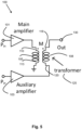
- FIG. 8 and FIG. 9 A schematic illustration of an example of the power amplifier arrangement 100 with a Wilkinson power amplifier 140 is shown in FIG. 8 and FIG. 9 .
- FIG. 9 is a more detailed example of the power amplifier 100 in FIG. 8 .
- the power amplifier arrangement 100 may instead comprise a power amplifier with two transmission lines, i.e. the Wilkinson power divider 140 may be replaced by a power divider with two transmission lines.
- FIG. 8 shows that the power amplifier arrangement 100 comprises a main amplifier 101 , an auxiliary amplifier 103 , a transformer 125 and a Wilkinson power divider 140 .
- the two paths in the Wilkinson power divider 140 in FIG. 8 may be based on ⁇ /4 transmission lines and the resistance may be a 1000.
- the main amplifier 101 may comprise a main input impedance matching network IIM 1 801 , a main output impedance matching OIM 1 803 , and a transistor Q 1 with a gate resistance R 1 .
- the source of the transistor is grounded.
- V Gm is the gate bias.
- the auxiliary amplifier 103 exemplified in FIG.
- the transformer 8 comprises an auxiliary input impedance matching network IIM 2 808 , an auxiliary output impedance matching OIM 1 810 , and a transistor Q 2 with a gate resistance R 1 .
- the source of Q 2 is grounded t00.
- V Ga is the gate bias.
- the transformer 125 comprises a first transmission line TL 1 and a second transmission line TL 2 .
- the first transmission line TL 1 is connected to ground at one end, and the second transmission line TL 2 is connected to the load 130 at one end.
- the term output refers to the output of the power amplifier arrangement 100 .
- FIG. 9 shows an example of the power amplifier arrangement 100 with more details compared to FIG. 8 .
- a Wilkinson power divider 140 may split the input power into two parts to drive the main amplifier 101 and the auxiliary amplifier 103 separately.
- the power amplifier arrangement 100 in FIG. 9 is a single-stage power amplifier arrangement.
- the two paths in the Wilkinson power divider 140 may be based on ⁇ /4 transmission lines and the resistance may be 100Q.
- the input impedance matching network IIM 1 801 may comprise transmission lines TL 1 TL 2 , TL 3 , as well as a capacitor C 1 .
- Transmission line TL 4 and capacitor C 2 are used for output impedance matching OIM 1 803 between the drain of Q 1 and the transformer 125 .
- the input impedance matching network IIM 2 808 comprises transmission lines TL 5 , TL 6 , TL 7 , as well as a capacitor, C 11 .
- Transmission line TL 8 and a capacitor C 22 is used for the output impedance matching OIM 2 810 between the drain of Q 2 and the transformer 125 .
- Coupled lines TL 9 and TL 10 form a Doherty combiner (transformer). One terminal of TL 9 is grounded and the other one is connected with the drain of Q 1 via capacitor C 2 .
- FIG. 9 also shows gate resistor R 1 , and gate biases V Gm , V Ga , as well as drain supply voltage V DD .
- the power amplifier arrangement 100 may be a single stage power amplifier arrangement, a two-stage power amplifier arrangement or a multi-stage power amplifier.
- a single stage power amplifier arrangement may have a lower gain compared to a two-stage power amplifier arrangement.
- a schematic example of a two-stage power amplifier arrangement is shown in FIG. 10 where Wilkinson power divider is replaced by two transmission lines connected with the input port in order to reduce the losses.
- the impedances of the first stage of the main amplifier 101 and the auxiliary amplifier 103 are matched to 100 ⁇ .
- a 40 GHz power amplifier arrangement 100 as shown in FIG. 10 may be implemented in a 60 nm GaN technology.
- a Lange coupler may be used as a transformer 125 to increase the coupling coefficient of the transformer 125 .
- the size of the power amplifier arrangement 100 may be for example 1.13 ⁇ 1.44 mm 2 .
- FIG. 11 plots the gain versus output power at example frequencies 38.0 GHz, 39.3 GHz, 40.6 GHz, as well as 42.0 GHz for a two-stage power amplifier arrangement 100 with a two transmission lines divider.
- the x-axis of FIG. 11 represents output power, P out , measured in dBm.
- the y-axis of FIG. 11 represents the gain measured in dB.
- the small signal gain of the power amplifier arrangement 100 is varied between 16.0 dB to 17.4 dB at different frequencies. As the output power of the power amplifier arrangement 100 increases, the gain of the power amplifier arrangement 100 reduces no more than 3 dB for the given frequencies.
- the maximum output power of the power amplifier arrangement 100 is around 31 dBm.
- PAEs of the power amplifier arrangement 100 at example frequencies 38.0 GHz, 39.3 GHz, 40.6 GHz, and 42.0 GHz are plotted in FIG. 12 .
- the x-axis of FIG. 12 represents P out measured in dBm and the y-axis represents PAE in %.
- the maximum PAEs varies between 35% to 38.5% at different frequencies, and the PAE at 6 dB output power back-off (PBO) varies between 26% to 28%. Details of the PAEs at output power equal to 25 dBm and 31 dBm are listed in Table 1 below:
- FIG. 13 shows a block diagram for an electronic circuit 200 or an electronic apparatus 200 .
- the electronic circuit or apparatus 200 comprises the power amplifier arrangement 100 of FIGS. 5 - 10 .
- the electronic circuit or apparatus 200 may be a transmitter, a transceiver or a unit having transmitting capabilities in a communications system or network.
- the electronic apparatus 200 may comprise other units, where a memory 203 and a processing unit 201 are shown in FIG. 13 .
- the electronic apparatus 200 may be a user equipment (UE), a mobile device, a communication device, a base station, a radar device etc.
- UE user equipment
- the memory 203 comprises one or more memory units.
- the memory 203 is arranged to be used to store data, power level measurements, output, input, RF signals, input power, output power, impedance information, capacitance information, arrangement information, threshold values, time periods, configurations, schedulings, and applications to perform the methods herein when being executed in the electronic circuit 200 or the electronic apparatus 200 .
- the processing unit 201 may be for example a Digital Signal Processor (DSP), Application Specific Integrated Circuit (ASIC) processor, Field-programmable gate array (FPGA) processor or microprocessor.
- DSP Digital Signal Processor
- ASIC Application Specific Integrated Circuit
- FPGA Field-programmable gate array
- the program code mentioned above may also be provided as a computer program product, for instance in the form of a data carrier carrying computer program code for performing the embodiments herein when being loaded into the electronic circuit 200 and/or the electronic apparatus 200 .
- One such carrier may be in the form of a CD ROM disc. It is however feasible with other data carriers such as a memory stick.
- the computer program code can furthermore be provided as pure program code on a server and downloaded to the electronic circuit 200 and/or the electronic apparatus 200 .
- a power amplifier arrangement 100 comprises a main amplifier 101 .
- the main amplifier 101 comprises an output connected to a first terminal 110 of a primary winding 105 of a transformer 125 .
- a second terminal 113 of the primary winding 105 is connected to ground 115 .
- the main amplifier 101 comprises an output connected to one terminal 110 of the primary winding 105 of the transformer, and another terminal 115 of the primary winding 105 is connected to ground 115 .
- the power amplifier arrangement 100 comprises an auxiliary amplifier 103 .
- the auxiliary amplifier 103 comprises an output connected to a first terminal 120 of a secondary winding 108 of the transformer 125 .
- a second terminal 118 of the secondary winding 108 is connected to a load 130 .
- the auxiliary amplifier 103 comprises an output connected to one terminal 120 of the secondary winding of the transformer 125 , and another terminal 118 of the secondary winding 108 is connected to the load 130 .
- the transformer 125 comprises two windings and four terminals 110 , 113 , 118 , 120 .
- the primary winding 105 comprises two terminals, i.e. the first terminal 110 and the second terminal 113 of the primary winding 105 .
- the secondary winding 108 comprises two terminals, i.e. the first terminal 120 and the second terminal 118 of the secondary winding 108 .
- the terminals 118 , 120 of the secondary winding 108 may also be referred to as a third terminal 120 and a fourth terminal 118 , where the third terminal 120 is the one connected to the output of the auxiliary amplifier 103 and where the fourth terminal 118 is the one connected load 130 .
- the terms first, second, third and fourth is associated with that the transformer 125 in total comprises four terminals.
- the main amplifier 101 may be driven by a first RF signal.
- the auxiliary amplifier 103 may be driven by a second RF signal.
- the first and second RF signals may be RF-signals that are in-phase.
- the power amplifier arrangement 100 may comprise a power divider 140 adapted to divide input power into a first input power to be input to the first amplifier 101 and a second input power to be input to the auxiliary amplifier 103 .
- the power divider 140 may comprise isolation between a first output port providing the first input power and a second output port providing the second input power.
- the power divider 140 may be a Wilkinson power divider or a power divider comprising at least two transmission lines.
- the term “at least two” may be used interchangeably with multiple or a plurality and indicates that there may be two or more transmission lines.
- a two-way power divider comprises at least two transmission lines. For a wide bandwidth, the power divider may comprise more than two transmission lines connected in series.
- Outputs from the main amplifier 101 and the auxiliary amplifier 103 may be added in-phase by the primary winding 105 and the secondary winding 108 when both the main amplifier 101 and the auxiliary amplifier 103 are in an on state and when the power amplifier arrangement operates in a high-input-power region.
- the power amplifier arrangement 100 may be a single stage power amplifier arrangement or a multi-stage power amplifier arrangement.
- the main amplifier 101 may comprise a first input impedance matching network 801 and a first output impedance matching network 803 .
- the second amplifier 103 may comprise a second input impedance matching network 808 and a second output impedance matching network 810 .
- the first input impedance matching network 801 may comprise one or multiple transmission lines and one or multiple capacitors.
- the first output impedance matching network 803 may comprise one or multiple transmission lines and one or multiple capacitors.
- the second input impedance matching network 808 may comprise one or multiple transmission lines and one or multiple capacitors.
- the second output impedance matching network 810 may comprise one or multiple transmission lines and one or multiple capacitors.
- the transformer 125 may be at least one of: edge-side coupled, and/or broad side coupled and/or coupled.
- the primary winding 105 and the secondary winding 108 may be at least one of: edge-side coupled, and/or broad side coupled and/or coupled.
- the power amplifier arrangement 100 has multi metal layers, all coupling types may be be used. If the power amplifier arrangement 100 has only one-metal layer, then, the edge-side coupled type may be used only. Broad side coupling has a relative large coupling between two windings 105 , 108 .
- the power amplifier arrangement 100 may be Doherty power amplifier arrangement.
- An electronic circuit 200 may comprise the power amplifier arrangement 100 described herein.
- An electronic device 200 may comprise the power amplifier arrangement 100 described herein.
- the embodiments herein relates to a transformer based Doherty power amplifier arrangement 100 .
- the embodiments herein relates to a power amplifier arrangement 100 comprising a single transformer 100 .
- the main amplifier 101 and the auxiliary amplifier 103 are connected with the primary and the secondary windings 105 , 108 , separately.
- One terminal of the primary winding 105 is grounded.
- One terminal of the secondary winding 108 is connected with outside load 130 .
- the main amplifier 101 and the auxiliary amplifier 103 are driven by two in-phase RF signals.
- a and B should be understood to mean “only A, only B, or both A and B.”, where A and B are any parameter, number, indication used herein etc.
Landscapes
- Engineering & Computer Science (AREA)
- Power Engineering (AREA)
- Microelectronics & Electronic Packaging (AREA)
- Amplifiers (AREA)
Abstract
Description
I 1 =I 2 (1a)
V m =V L −V a (1b)
where I1 and I2 are currents following through the primary winding 105 and the secondary winding 108, respectively, and where VL is the voltage at the load RL 130:
V L =R L I 2 (2)
| TABLE 1 | ||||||
| Pout | ||||||
| (dBm) | 38.0 GHz | 39.3 GHz | 40.6 GHz | 42.0 |
||
| 25 | 26.3% | 27.0% | 28.0% | 27.0% | ||
| 31 | 35.0% | 37.9% | 38.4% | 36.5% | ||
Claims (19)
Applications Claiming Priority (1)
| Application Number | Priority Date | Filing Date | Title |
|---|---|---|---|
| PCT/EP2019/056302 WO2020182305A1 (en) | 2019-03-13 | 2019-03-13 | Power amplifier arrangement |
Publications (2)
| Publication Number | Publication Date |
|---|---|
| US20220006429A1 US20220006429A1 (en) | 2022-01-06 |
| US12155352B2 true US12155352B2 (en) | 2024-11-26 |
Family
ID=65812301
Family Applications (1)
| Application Number | Title | Priority Date | Filing Date |
|---|---|---|---|
| US17/432,779 Active 2040-11-23 US12155352B2 (en) | 2019-03-13 | 2019-03-13 | Power amplifier arrangement |
Country Status (3)
| Country | Link |
|---|---|
| US (1) | US12155352B2 (en) |
| EP (1) | EP3939161A1 (en) |
| WO (1) | WO2020182305A1 (en) |
Cited By (1)
| Publication number | Priority date | Publication date | Assignee | Title |
|---|---|---|---|---|
| US20230327312A1 (en) * | 2020-09-01 | 2023-10-12 | Telefonaktiebolaget Lm Ericsson (Publ) | Radio frequency power divider and circuit including the same |
Families Citing this family (11)
| Publication number | Priority date | Publication date | Assignee | Title |
|---|---|---|---|---|
| US12375041B2 (en) * | 2020-10-02 | 2025-07-29 | Qualcomm Incorporated | Distributed active power combining amplifier |
| WO2022122115A1 (en) * | 2020-12-07 | 2022-06-16 | Telefonaktiebolaget Lm Ericsson (Publ) | An amplifier arrangement with enhanced harmonic rejection |
| DE102021102872B3 (en) * | 2021-02-08 | 2022-08-04 | RWTH Aachen University, Körperschaft des öffentlichen Rechts | Doherty amplifier circuit and method of operating a Doherty amplifier circuit |
| US12603622B2 (en) * | 2021-10-29 | 2026-04-14 | Analog Devices International Unlimited Company | Apparatus and methods for radio frequency amplifiers |
| US20250158571A1 (en) * | 2022-02-09 | 2025-05-15 | Georgia Tech Research Corporation | Broadband coupler-based balun continuous active load modulation power amplifier |
| WO2023153964A1 (en) * | 2022-02-11 | 2023-08-17 | Telefonaktiebolaget Lm Ericsson (Publ) | A configurable doherty power amplifier arrangement |
| CN218829865U (en) * | 2022-11-28 | 2023-04-07 | 深圳飞骧科技股份有限公司 | Radio frequency power amplifier and radio frequency chip |
| CN116647199B (en) * | 2023-07-24 | 2023-11-07 | 成都通量科技有限公司 | Tuning transformer and Doherty power amplifier comprising same |
| KR102850842B1 (en) * | 2023-11-20 | 2025-08-25 | 고려대학교 산학협력단 | Wideband series-parallel combined power amplifier using transformer with grounded center tap technique |
| CN118157594A (en) * | 2024-02-08 | 2024-06-07 | 北京昂瑞微电子技术股份有限公司 | Broadband Doherty Power Amplifier |
| US20250357896A1 (en) * | 2024-05-15 | 2025-11-20 | Qualcomm Incorporated | Concurrent matching transceiver for power amplifier |
Citations (8)
| Publication number | Priority date | Publication date | Assignee | Title |
|---|---|---|---|---|
| US6057731A (en) * | 1998-09-23 | 2000-05-02 | Nortel Networks Corporation | Low-distortion high-frequency amplifier |
| US6889034B1 (en) * | 1998-04-02 | 2005-05-03 | Ericsson Inc. | Antenna coupling systems and methods for transmitters |
| US20100103043A1 (en) * | 2006-10-03 | 2010-04-29 | Milano Alberto | Phased shifted oscilator and antenna |
| US8975955B2 (en) * | 2012-12-11 | 2015-03-10 | Alcatel Lucent | Analysis of Doherty amplifiers |
| US20150200435A1 (en) * | 2012-10-22 | 2015-07-16 | Fernando Pinheiro Guimaraes | Method and system for providing improved high power rf splitter/combiner |
| US9467115B2 (en) | 2014-05-13 | 2016-10-11 | Skyworks Solutions, Inc. | Circuits, devices and methods related to combiners for Doherty power amplifiers |
| EP3343762A1 (en) | 2016-12-29 | 2018-07-04 | NXP USA, Inc. | Doherty amplifiers with passive phase compensation circuits |
| US20190131938A1 (en) * | 2017-10-31 | 2019-05-02 | Nxp B.V. | Power amplifier cell |
-
2019
- 2019-03-13 EP EP19711558.7A patent/EP3939161A1/en active Pending
- 2019-03-13 WO PCT/EP2019/056302 patent/WO2020182305A1/en not_active Ceased
- 2019-03-13 US US17/432,779 patent/US12155352B2/en active Active
Patent Citations (8)
| Publication number | Priority date | Publication date | Assignee | Title |
|---|---|---|---|---|
| US6889034B1 (en) * | 1998-04-02 | 2005-05-03 | Ericsson Inc. | Antenna coupling systems and methods for transmitters |
| US6057731A (en) * | 1998-09-23 | 2000-05-02 | Nortel Networks Corporation | Low-distortion high-frequency amplifier |
| US20100103043A1 (en) * | 2006-10-03 | 2010-04-29 | Milano Alberto | Phased shifted oscilator and antenna |
| US20150200435A1 (en) * | 2012-10-22 | 2015-07-16 | Fernando Pinheiro Guimaraes | Method and system for providing improved high power rf splitter/combiner |
| US8975955B2 (en) * | 2012-12-11 | 2015-03-10 | Alcatel Lucent | Analysis of Doherty amplifiers |
| US9467115B2 (en) | 2014-05-13 | 2016-10-11 | Skyworks Solutions, Inc. | Circuits, devices and methods related to combiners for Doherty power amplifiers |
| EP3343762A1 (en) | 2016-12-29 | 2018-07-04 | NXP USA, Inc. | Doherty amplifiers with passive phase compensation circuits |
| US20190131938A1 (en) * | 2017-10-31 | 2019-05-02 | Nxp B.V. | Power amplifier cell |
Non-Patent Citations (8)
| Title |
|---|
| Ahn, H. et al., "A Highly Efficient WLAN CMOS PA with Two-Winding and Single-Winding Combined Transformer", IEEE Radio Frequency Integrated Circuits Symposium, May 2016, pp. 310-313. |
| Chen, D. et al., "A V-Band Doherty Power Amplifier Based on Voltage Combination and Balance Compensation Marchand Balun", IEEE Access, Mar. 15, 2018, pp. 10131-10138, vol. 6. |
| Cho, Y. et al., "Voltage-Combined CMOS Doherty Power Amplifier Based on Transformer", IEEE Transactions on Microwave Theory and Techniques, Nov. 2016, pp. 3612-3622, vol. 64, No. 11. |
| Hu, S. et al., "Design of a Transformer-Based Reconfigurable Digital Polar Doherty Power Amplifier Fully Integrated in Bulk CMOS", IEEE Journal of Solid-State Circuits, May 2015, pp. 1094-1106, vol. 50, No. 5. |
| Kaymaksut, E., "Transformer-Based Doherty Power Amplifiers for mm-Wave Applications in 40-nm CMOS", IEEE Transactions on Microwave Theory and Techniques, Apr. 2015, pp. 1186-1192, vol. 63, No. 4. |
| Kaymaksut, E., "Transformer-Based Uneven Doherty Power Amplifier in 90 nm CMOS for WLAN Applications", EEE Journal of Solid-State Circuits, Jul. 2012, pp. 1659-1671, vol. 47, No. 7. |
| Vorapipat, V. et al., "A Class-G Voltage-Mode Doherty Power Amplifier", IEEE Journal of Solid-State Circuits, Dec. 2017, pp. 3348-3360, vol. 52, No. 12. |
| Yin, Y. et al., "A Compact Dual-Band Digital Doherty Power Amplifier Using Parallel-Combining Transformer for Cellular NB-IoT Applications", IEEE International Solid-State Circuits Conference, Feb. 14, 2018, pp. 407-409. |
Cited By (1)
| Publication number | Priority date | Publication date | Assignee | Title |
|---|---|---|---|---|
| US20230327312A1 (en) * | 2020-09-01 | 2023-10-12 | Telefonaktiebolaget Lm Ericsson (Publ) | Radio frequency power divider and circuit including the same |
Also Published As
| Publication number | Publication date |
|---|---|
| EP3939161A1 (en) | 2022-01-19 |
| US20220006429A1 (en) | 2022-01-06 |
| WO2020182305A1 (en) | 2020-09-17 |
Similar Documents
| Publication | Publication Date | Title |
|---|---|---|
| US12155352B2 (en) | Power amplifier arrangement | |
| US9899962B2 (en) | Power amplifier | |
| US10601382B2 (en) | Power amplifier circuit | |
| EP3054589B1 (en) | Doherty amplifier | |
| US10483918B2 (en) | Doherty power amplifier for radio-frequency applications | |
| US8912846B2 (en) | Doherty amplifier arrangement | |
| KR20230007556A (en) | Systems and methods related to linear and efficient broadband power amplifiers | |
| US11223327B2 (en) | Power amplifier | |
| US20140306780A1 (en) | Duplexers | |
| US20230216456A1 (en) | Power amplifier circuit | |
| US12574064B2 (en) | Radio frequency circuit, radio frequency module, and communication device | |
| US11303249B2 (en) | Consecutive doherty amplifier | |
| US9515613B2 (en) | Dual-band doherty amplifier and method therefor | |
| CN113994592B (en) | Power amplifier with high output power | |
| Essing et al. | A fully integrated 60GHz distributed transformer power amplifier in bulky CMOS 45nm | |
| KR102934384B1 (en) | Power amplifier and drive amplifier | |
| US9385663B2 (en) | Envelope tracking push-pull or differential power amplifier | |
| US12525920B2 (en) | Input matching network with harmonic trap for frequency multiplier | |
| Liu et al. | A 25-40 GHz Three-Way Power Amplifier with No Load Modulation Achieving Broadband Deep Power Back-Off Efficiency Enhancement | |
| US20250202435A1 (en) | Amplifier circuit | |
| US20250141409A1 (en) | A configurable doherty power amplifier arrangement | |
| US20250030388A1 (en) | Power combiner for power amplifier | |
| WO2025105179A1 (en) | Power amplification circuit |
Legal Events
| Date | Code | Title | Description |
|---|---|---|---|
| AS | Assignment |
Owner name: TELEFONAKTIEBOLAGET LM ERICSSON (PUBL), SWEDEN Free format text: ASSIGNMENT OF ASSIGNORS INTEREST;ASSIGNORS:BAO, MINGQUAN;GUSTAFSSON, DAVID;ANDERSSON, KRISTOFFER;SIGNING DATES FROM 20190314 TO 20190315;REEL/FRAME:057243/0430 |
|
| FEPP | Fee payment procedure |
Free format text: ENTITY STATUS SET TO UNDISCOUNTED (ORIGINAL EVENT CODE: BIG.); ENTITY STATUS OF PATENT OWNER: LARGE ENTITY |
|
| STPP | Information on status: patent application and granting procedure in general |
Free format text: DOCKETED NEW CASE - READY FOR EXAMINATION |
|
| STPP | Information on status: patent application and granting procedure in general |
Free format text: NON FINAL ACTION MAILED |
|
| STPP | Information on status: patent application and granting procedure in general |
Free format text: RESPONSE TO NON-FINAL OFFICE ACTION ENTERED AND FORWARDED TO EXAMINER |
|
| STPP | Information on status: patent application and granting procedure in general |
Free format text: FINAL REJECTION MAILED |
|
| STPP | Information on status: patent application and granting procedure in general |
Free format text: ADVISORY ACTION MAILED |
|
| STCV | Information on status: appeal procedure |
Free format text: NOTICE OF APPEAL FILED |
|
| STPP | Information on status: patent application and granting procedure in general |
Free format text: RESPONSE TO NON-FINAL OFFICE ACTION ENTERED AND FORWARDED TO EXAMINER |
|
| STPP | Information on status: patent application and granting procedure in general |
Free format text: NOTICE OF ALLOWANCE MAILED -- APPLICATION RECEIVED IN OFFICE OF PUBLICATIONS |
|
| ZAAB | Notice of allowance mailed |
Free format text: ORIGINAL CODE: MN/=. |
|
| STPP | Information on status: patent application and granting procedure in general |
Free format text: PUBLICATIONS -- ISSUE FEE PAYMENT RECEIVED |
|
| STCF | Information on status: patent grant |
Free format text: PATENTED CASE |