US12148395B2 - Display device and method of operating the same - Google Patents
Display device and method of operating the same Download PDFInfo
- Publication number
- US12148395B2 US12148395B2 US18/102,794 US202318102794A US12148395B2 US 12148395 B2 US12148395 B2 US 12148395B2 US 202318102794 A US202318102794 A US 202318102794A US 12148395 B2 US12148395 B2 US 12148395B2
- Authority
- US
- United States
- Prior art keywords
- image data
- correction value
- color coordinate
- luminance
- input image
- Prior art date
- Legal status (The legal status is an assumption and is not a legal conclusion. Google has not performed a legal analysis and makes no representation as to the accuracy of the status listed.)
- Active, expires
Links
- 238000000034 method Methods 0.000 title claims description 20
- 238000012937 correction Methods 0.000 claims description 172
- 230000004044 response Effects 0.000 claims description 8
- 238000010586 diagram Methods 0.000 description 14
- 238000009877 rendering Methods 0.000 description 5
- 230000008859 change Effects 0.000 description 4
- 101001116668 Homo sapiens Prefoldin subunit 3 Proteins 0.000 description 3
- 102100024884 Prefoldin subunit 3 Human genes 0.000 description 3
- 238000006243 chemical reaction Methods 0.000 description 3
- 238000012986 modification Methods 0.000 description 3
- 230000004048 modification Effects 0.000 description 3
- 238000012545 processing Methods 0.000 description 3
- 230000008901 benefit Effects 0.000 description 2
- 239000003990 capacitor Substances 0.000 description 2
- 238000004891 communication Methods 0.000 description 2
- 239000002096 quantum dot Substances 0.000 description 2
- 101100368149 Mus musculus Sync gene Proteins 0.000 description 1
- 208000006930 Pseudomyxoma Peritonei Diseases 0.000 description 1
- 230000005540 biological transmission Effects 0.000 description 1
- 230000007423 decrease Effects 0.000 description 1
- 230000006870 function Effects 0.000 description 1
- 239000011159 matrix material Substances 0.000 description 1
- 230000002093 peripheral effect Effects 0.000 description 1
- 229920000642 polymer Polymers 0.000 description 1
- 229920000306 polymethylpentene Polymers 0.000 description 1
- 239000007787 solid Substances 0.000 description 1
- 230000003068 static effect Effects 0.000 description 1
- 230000009466 transformation Effects 0.000 description 1
Images


Classifications
-
- G—PHYSICS
- G09—EDUCATION; CRYPTOGRAPHY; DISPLAY; ADVERTISING; SEALS
- G09G—ARRANGEMENTS OR CIRCUITS FOR CONTROL OF INDICATING DEVICES USING STATIC MEANS TO PRESENT VARIABLE INFORMATION
- G09G3/00—Control arrangements or circuits, of interest only in connection with visual indicators other than cathode-ray tubes
- G09G3/20—Control arrangements or circuits, of interest only in connection with visual indicators other than cathode-ray tubes for presentation of an assembly of a number of characters, e.g. a page, by composing the assembly by combination of individual elements arranged in a matrix no fixed position being assigned to or needed to be assigned to the individual characters or partial characters
- G09G3/22—Control arrangements or circuits, of interest only in connection with visual indicators other than cathode-ray tubes for presentation of an assembly of a number of characters, e.g. a page, by composing the assembly by combination of individual elements arranged in a matrix no fixed position being assigned to or needed to be assigned to the individual characters or partial characters using controlled light sources
- G09G3/30—Control arrangements or circuits, of interest only in connection with visual indicators other than cathode-ray tubes for presentation of an assembly of a number of characters, e.g. a page, by composing the assembly by combination of individual elements arranged in a matrix no fixed position being assigned to or needed to be assigned to the individual characters or partial characters using controlled light sources using electroluminescent panels
- G09G3/32—Control arrangements or circuits, of interest only in connection with visual indicators other than cathode-ray tubes for presentation of an assembly of a number of characters, e.g. a page, by composing the assembly by combination of individual elements arranged in a matrix no fixed position being assigned to or needed to be assigned to the individual characters or partial characters using controlled light sources using electroluminescent panels semiconductive, e.g. using light-emitting diodes [LED]
- G09G3/3208—Control arrangements or circuits, of interest only in connection with visual indicators other than cathode-ray tubes for presentation of an assembly of a number of characters, e.g. a page, by composing the assembly by combination of individual elements arranged in a matrix no fixed position being assigned to or needed to be assigned to the individual characters or partial characters using controlled light sources using electroluminescent panels semiconductive, e.g. using light-emitting diodes [LED] organic, e.g. using organic light-emitting diodes [OLED]
- G09G3/3275—Details of drivers for data electrodes
- G09G3/3291—Details of drivers for data electrodes in which the data driver supplies a variable data voltage for setting the current through, or the voltage across, the light-emitting elements
-
- G—PHYSICS
- G09—EDUCATION; CRYPTOGRAPHY; DISPLAY; ADVERTISING; SEALS
- G09G—ARRANGEMENTS OR CIRCUITS FOR CONTROL OF INDICATING DEVICES USING STATIC MEANS TO PRESENT VARIABLE INFORMATION
- G09G3/00—Control arrangements or circuits, of interest only in connection with visual indicators other than cathode-ray tubes
- G09G3/20—Control arrangements or circuits, of interest only in connection with visual indicators other than cathode-ray tubes for presentation of an assembly of a number of characters, e.g. a page, by composing the assembly by combination of individual elements arranged in a matrix no fixed position being assigned to or needed to be assigned to the individual characters or partial characters
- G09G3/22—Control arrangements or circuits, of interest only in connection with visual indicators other than cathode-ray tubes for presentation of an assembly of a number of characters, e.g. a page, by composing the assembly by combination of individual elements arranged in a matrix no fixed position being assigned to or needed to be assigned to the individual characters or partial characters using controlled light sources
- G09G3/30—Control arrangements or circuits, of interest only in connection with visual indicators other than cathode-ray tubes for presentation of an assembly of a number of characters, e.g. a page, by composing the assembly by combination of individual elements arranged in a matrix no fixed position being assigned to or needed to be assigned to the individual characters or partial characters using controlled light sources using electroluminescent panels
- G09G3/32—Control arrangements or circuits, of interest only in connection with visual indicators other than cathode-ray tubes for presentation of an assembly of a number of characters, e.g. a page, by composing the assembly by combination of individual elements arranged in a matrix no fixed position being assigned to or needed to be assigned to the individual characters or partial characters using controlled light sources using electroluminescent panels semiconductive, e.g. using light-emitting diodes [LED]
- G09G3/3208—Control arrangements or circuits, of interest only in connection with visual indicators other than cathode-ray tubes for presentation of an assembly of a number of characters, e.g. a page, by composing the assembly by combination of individual elements arranged in a matrix no fixed position being assigned to or needed to be assigned to the individual characters or partial characters using controlled light sources using electroluminescent panels semiconductive, e.g. using light-emitting diodes [LED] organic, e.g. using organic light-emitting diodes [OLED]
- G09G3/3225—Control arrangements or circuits, of interest only in connection with visual indicators other than cathode-ray tubes for presentation of an assembly of a number of characters, e.g. a page, by composing the assembly by combination of individual elements arranged in a matrix no fixed position being assigned to or needed to be assigned to the individual characters or partial characters using controlled light sources using electroluminescent panels semiconductive, e.g. using light-emitting diodes [LED] organic, e.g. using organic light-emitting diodes [OLED] using an active matrix
-
- G—PHYSICS
- G09—EDUCATION; CRYPTOGRAPHY; DISPLAY; ADVERTISING; SEALS
- G09G—ARRANGEMENTS OR CIRCUITS FOR CONTROL OF INDICATING DEVICES USING STATIC MEANS TO PRESENT VARIABLE INFORMATION
- G09G3/00—Control arrangements or circuits, of interest only in connection with visual indicators other than cathode-ray tubes
- G09G3/20—Control arrangements or circuits, of interest only in connection with visual indicators other than cathode-ray tubes for presentation of an assembly of a number of characters, e.g. a page, by composing the assembly by combination of individual elements arranged in a matrix no fixed position being assigned to or needed to be assigned to the individual characters or partial characters
- G09G3/22—Control arrangements or circuits, of interest only in connection with visual indicators other than cathode-ray tubes for presentation of an assembly of a number of characters, e.g. a page, by composing the assembly by combination of individual elements arranged in a matrix no fixed position being assigned to or needed to be assigned to the individual characters or partial characters using controlled light sources
- G09G3/30—Control arrangements or circuits, of interest only in connection with visual indicators other than cathode-ray tubes for presentation of an assembly of a number of characters, e.g. a page, by composing the assembly by combination of individual elements arranged in a matrix no fixed position being assigned to or needed to be assigned to the individual characters or partial characters using controlled light sources using electroluminescent panels
- G09G3/32—Control arrangements or circuits, of interest only in connection with visual indicators other than cathode-ray tubes for presentation of an assembly of a number of characters, e.g. a page, by composing the assembly by combination of individual elements arranged in a matrix no fixed position being assigned to or needed to be assigned to the individual characters or partial characters using controlled light sources using electroluminescent panels semiconductive, e.g. using light-emitting diodes [LED]
- G09G3/3208—Control arrangements or circuits, of interest only in connection with visual indicators other than cathode-ray tubes for presentation of an assembly of a number of characters, e.g. a page, by composing the assembly by combination of individual elements arranged in a matrix no fixed position being assigned to or needed to be assigned to the individual characters or partial characters using controlled light sources using electroluminescent panels semiconductive, e.g. using light-emitting diodes [LED] organic, e.g. using organic light-emitting diodes [OLED]
- G09G3/3266—Details of drivers for scan electrodes
-
- G—PHYSICS
- G09—EDUCATION; CRYPTOGRAPHY; DISPLAY; ADVERTISING; SEALS
- G09G—ARRANGEMENTS OR CIRCUITS FOR CONTROL OF INDICATING DEVICES USING STATIC MEANS TO PRESENT VARIABLE INFORMATION
- G09G5/00—Control arrangements or circuits for visual indicators common to cathode-ray tube indicators and other visual indicators
- G09G5/02—Control arrangements or circuits for visual indicators common to cathode-ray tube indicators and other visual indicators characterised by the way in which colour is displayed
-
- H—ELECTRICITY
- H04—ELECTRIC COMMUNICATION TECHNIQUE
- H04N—PICTORIAL COMMUNICATION, e.g. TELEVISION
- H04N9/00—Details of colour television systems
- H04N9/64—Circuits for processing colour signals
- H04N9/67—Circuits for processing colour signals for matrixing
-
- G—PHYSICS
- G09—EDUCATION; CRYPTOGRAPHY; DISPLAY; ADVERTISING; SEALS
- G09G—ARRANGEMENTS OR CIRCUITS FOR CONTROL OF INDICATING DEVICES USING STATIC MEANS TO PRESENT VARIABLE INFORMATION
- G09G2310/00—Command of the display device
- G09G2310/02—Addressing, scanning or driving the display screen or processing steps related thereto
- G09G2310/0264—Details of driving circuits
- G09G2310/0278—Details of driving circuits arranged to drive both scan and data electrodes
-
- G—PHYSICS
- G09—EDUCATION; CRYPTOGRAPHY; DISPLAY; ADVERTISING; SEALS
- G09G—ARRANGEMENTS OR CIRCUITS FOR CONTROL OF INDICATING DEVICES USING STATIC MEANS TO PRESENT VARIABLE INFORMATION
- G09G2320/00—Control of display operating conditions
- G09G2320/02—Improving the quality of display appearance
- G09G2320/0233—Improving the luminance or brightness uniformity across the screen
-
- G—PHYSICS
- G09—EDUCATION; CRYPTOGRAPHY; DISPLAY; ADVERTISING; SEALS
- G09G—ARRANGEMENTS OR CIRCUITS FOR CONTROL OF INDICATING DEVICES USING STATIC MEANS TO PRESENT VARIABLE INFORMATION
- G09G2320/00—Control of display operating conditions
- G09G2320/02—Improving the quality of display appearance
- G09G2320/0242—Compensation of deficiencies in the appearance of colours
-
- G—PHYSICS
- G09—EDUCATION; CRYPTOGRAPHY; DISPLAY; ADVERTISING; SEALS
- G09G—ARRANGEMENTS OR CIRCUITS FOR CONTROL OF INDICATING DEVICES USING STATIC MEANS TO PRESENT VARIABLE INFORMATION
- G09G2320/00—Control of display operating conditions
- G09G2320/02—Improving the quality of display appearance
- G09G2320/0247—Flicker reduction other than flicker reduction circuits used for single beam cathode-ray tubes
-
- G—PHYSICS
- G09—EDUCATION; CRYPTOGRAPHY; DISPLAY; ADVERTISING; SEALS
- G09G—ARRANGEMENTS OR CIRCUITS FOR CONTROL OF INDICATING DEVICES USING STATIC MEANS TO PRESENT VARIABLE INFORMATION
- G09G2320/00—Control of display operating conditions
- G09G2320/02—Improving the quality of display appearance
- G09G2320/0271—Adjustment of the gradation levels within the range of the gradation scale, e.g. by redistribution or clipping
-
- G—PHYSICS
- G09—EDUCATION; CRYPTOGRAPHY; DISPLAY; ADVERTISING; SEALS
- G09G—ARRANGEMENTS OR CIRCUITS FOR CONTROL OF INDICATING DEVICES USING STATIC MEANS TO PRESENT VARIABLE INFORMATION
- G09G2320/00—Control of display operating conditions
- G09G2320/06—Adjustment of display parameters
- G09G2320/0626—Adjustment of display parameters for control of overall brightness
-
- G—PHYSICS
- G09—EDUCATION; CRYPTOGRAPHY; DISPLAY; ADVERTISING; SEALS
- G09G—ARRANGEMENTS OR CIRCUITS FOR CONTROL OF INDICATING DEVICES USING STATIC MEANS TO PRESENT VARIABLE INFORMATION
- G09G2320/00—Control of display operating conditions
- G09G2320/06—Adjustment of display parameters
- G09G2320/0666—Adjustment of display parameters for control of colour parameters, e.g. colour temperature
-
- G—PHYSICS
- G09—EDUCATION; CRYPTOGRAPHY; DISPLAY; ADVERTISING; SEALS
- G09G—ARRANGEMENTS OR CIRCUITS FOR CONTROL OF INDICATING DEVICES USING STATIC MEANS TO PRESENT VARIABLE INFORMATION
- G09G2340/00—Aspects of display data processing
- G09G2340/04—Changes in size, position or resolution of an image
- G09G2340/0407—Resolution change, inclusive of the use of different resolutions for different screen areas
- G09G2340/0435—Change or adaptation of the frame rate of the video stream
-
- G—PHYSICS
- G09—EDUCATION; CRYPTOGRAPHY; DISPLAY; ADVERTISING; SEALS
- G09G—ARRANGEMENTS OR CIRCUITS FOR CONTROL OF INDICATING DEVICES USING STATIC MEANS TO PRESENT VARIABLE INFORMATION
- G09G2340/00—Aspects of display data processing
- G09G2340/06—Colour space transformation
-
- G—PHYSICS
- G09—EDUCATION; CRYPTOGRAPHY; DISPLAY; ADVERTISING; SEALS
- G09G—ARRANGEMENTS OR CIRCUITS FOR CONTROL OF INDICATING DEVICES USING STATIC MEANS TO PRESENT VARIABLE INFORMATION
- G09G5/00—Control arrangements or circuits for visual indicators common to cathode-ray tube indicators and other visual indicators
- G09G5/10—Intensity circuits
Definitions
- the present disclosure generally relates to a display device. More particularly, the present disclosure relates to a display device capable of supporting a variable frame mode and a driving method of the same.
- a display device displays an image at a constant frame rate (or a constant frame frequency) of 60 Hz or higher.
- the frame rate of rendering by the host processor e.g., a graphic processing unit (GPU) or graphics card
- the host processor provides frame data for a game image that performs complex rendering to the display device
- this frame rate mismatch may intensify, and a tearing phenomenon in which a boundary line is generated in an image displayed on the display device may occur due to a frame rate mismatch.
- variable frame mode e.g., free-sync mode, G-sync mode, Q-sync mode, etc.
- a host processor provides frame data to the display device at a variable frame rate (or a variable input frame frequency).
- the display device supporting the variable frame mode may prevent the tearing phenomenon by displaying an image in synchronization with the variable frame rate.
- the luminance of a display panel driven at a first frame frequency and the luminance of the display panel driven at a second frame frequency different from the first frame frequency may be different from each other. Accordingly, flicker may occur when the frame frequency of the display device is changed.
- Embodiment provides a display device with improved display quality.
- Embodiment provides a method of driving the display device.
- a display device may include a display panel including a plurality of pixels respectively connected to a plurality of scan lines and a plurality of data lines, a scan driver configured to provide scan signals to the pixels through the scan lines, a date driver configured to data voltages to the pixels through the data lines, and a controller configured to control the scan driver and the date driver, and including an image data processor configured to receive input image data at variable input frame frequency.
- the image data processor may determine a first correction value for correcting a luminance of the display panel according to the variable input frame frequency, determine a second correction value for correcting color coordinate values for components of the input image date to which the first correction value is reflected, and output an output image date obtained by adding the input image data to which the first correction value is reflected and the second correction value.
- the image data processor may determine a corrected color coordinate value for any one of the components, determine corrected color coordinate values for remaining components in response to the corrected color coordinate value for the one the component, and determine the second correction value based on the corrected color coordinate values for the one component and the remaining components.
- the image data processor may determine the corrected color coordinate value for the remaining components by applying a correction ratio for the one component to an original color coordinate value for the remaining components.
- the image data processor may determine the corrected color coordinate value for the remaining components such that a Lab color difference between the input image data to which the first correction value is reflected and the output image data in a Lab color space is minimized when the original color coordinate value of the one component is corrected with the corrected color coordinate value.
- the image data processor may include a first correction value determiner including a plurality of lookup tables for storing the different first correction values and configured to determine the first correction value for correcting the input image data by referring to a lookup table corresponding to the variable input frame frequency among the lookup tables, a second correction value determiner configured to converts color coordinate values of RGB components of the input image data to which the first correction value is reflected into color coordinate values of a Lab color space to determine the second correction value, and an image data corrector configured to output the output mage data.
- a first correction value determiner including a plurality of lookup tables for storing the different first correction values and configured to determine the first correction value for correcting the input image data by referring to a lookup table corresponding to the variable input frame frequency among the lookup tables
- a second correction value determiner configured to converts color coordinate values of RGB components of the input image data to which the first correction value is reflected into color coordinate values of a Lab color space to determine the second correction value
- an image data corrector configured to output the
- the image data processor may determine a minimum frequency as a reference frequency in a variable frequency range of the variable input frame frequency, determine a reference luminance by a luminance of the display panel at the reference frequency, and determine the first correction value based on the reference luminance corresponding to the reference frequency.
- a display device may include a display panel including a plurality of pixels respectively connected to a plurality of scan lines and a plurality of data lines, a scan driver configured to provide scan signals to the pixels through the scan lines, a date driver configured to data voltages to the pixels through the data lines, and a controller configured to control the scan driver and the date driver, and including an image data processor configured to receive input image data at variable input frame frequency.
- the image data processor may determine a first correction value for correcting a luminance of the display panel according to the variable input frame frequency, determine whether the luminance of the display panel is within any luminance range of a first luminance range and a second luminance range, determine a second correction value for correcting color coordinate values of components of the input image data to which the first correction value is reflected when the luminance of the display panel is within the first luminance range, and output an output image date obtained by adding the input image data to which the first correction value is reflected and the second correction value.
- the image data processor may determine the output image data obtained by adding the input image data and the first correction value when the luminance of the display panel falls within the second luminance.
- the first luminance range may be about 0.5 nit to about 4.5 nit and the second luminance range may be less than about 0.5 nit and greater than about 4.5 nit.
- the image data processor may determine a corrected color coordinate value for any one of the components, determine corrected color coordinate values for remaining components in response to the corrected color coordinate value for the one the component, and determine the second correction value based on the corrected color coordinate values for the one component and the remaining components.
- the image data processor may determine the corrected color coordinate value for the remaining components by applying a correction ratio for the one component to an original color coordinate value for the remaining components.
- the image data processor may determine the corrected color coordinate value for the remaining components such that a Lab color difference between the input image data to which the first correction value is reflected and the output image data in a Lab color space is minimized when the original color coordinate value of the one component is corrected with the corrected color coordinate value.
- the image data processor may include: a first correction value determiner including a plurality of lookup tables for storing the different first correction values and configured to determine the first correction value for correcting the input image data by referring to a lookup table corresponding to the variable input frame frequency among the lookup tables, a second correction value determiner configured to converts color coordinate values of RGB components of the input image data to which the first correction value is reflected into color coordinate values of a Lab color space to determine the second correction value, and an image data corrector configured to output the output mage data.
- a first correction value determiner including a plurality of lookup tables for storing the different first correction values and configured to determine the first correction value for correcting the input image data by referring to a lookup table corresponding to the variable input frame frequency among the lookup tables
- a second correction value determiner configured to converts color coordinate values of RGB components of the input image data to which the first correction value is reflected into color coordinate values of a Lab color space to determine the second correction value
- an image data corrector configured to output
- the image data processor may determine a minimum frequency as a reference frequency in a variable frequency range of the variable input frame frequency, determine a reference luminance by a luminance of the display panel at the reference frequency, and determine the first correction value based on the reference luminance corresponding to the reference frequency.
- a method of operating a display device receiving an input image data at a variable input frame frequency, determining a first correction value for correcting a luminance of a display panel according to the variable input frame frequency, determining a second correction value for correcting color coordinate values of components of the input image data to which the first correction value is reflected, and outputting an output image date obtained by adding the input image data to which the first correction value is reflected and the second correction value.
- the method may further include checking a luminance of the display panel based on the input image data after receiving the input image data.
- the determining the second correction value may include: determining a corrected color coordinate value for any one of the components, determining corrected color coordinate values for remaining components in response to the corrected color coordinate value for the one the component, and determining the second correction value based on the corrected color coordinate values for the one component and the remaining components.
- the determining corrected color values for the remaining components may include: determining the corrected color coordinate value for the remaining components by applying a correction ratio for the one component to an original color coordinate value for the remaining components.
- the determining corrected color values for the remaining components may include: determining the corrected color coordinate value for the remaining components such that a Lab color difference between the input image data to which the first correction value is reflected and the output image data in a Lab color space is minimized when the original color coordinate value of the one component is corrected with the corrected color coordinate value.
- the determining the first correction value may include: determining a minimum frequency as a reference frequency in a variable frequency range of the variable input frame frequency, determining a reference luminance by a luminance of the display panel at the reference frequency, and determining the first correction value based on the reference luminance corresponding to the reference frequency.
- an input image data may be received at a variable input frame frequency, a first correction value for correcting a luminance of a display panel according to the variable input frame frequency may be determined, a second correction value for correcting color coordinate values of components of the input image data to which the first correction value is reflected may be determined, and an output image date obtained by adding the input image data to which the first correction value is reflected and the second correction value may be output. Accordingly, a flicker may be minimized or reduced.
- FIG. 1 is a block diagram illustrating a display device according to an embodiment.
- FIG. 2 is a timing diagram illustrating an example of input image data input to the display device of FIG. 1 at a variable input frame frequency.
- FIG. 3 is a diagram illustrating an example of the luminance of a display panel driven at different frame frequencies when luminance correction is not performed.
- FIG. 4 is a diagram illustrating an example of the luminance of a display panel when luminance correction is not performed and an example of the luminance of a display panel when luminance correction is performed.
- FIG. 5 is a diagram illustrating an example of a color coordinate value according to the luminance of a display panel.
- FIG. 6 is a block diagram illustrating the image data processor of FIG. 1 .
- FIG. 7 is a flowchart illustrating a method of driving a display device according to an embodiment.
- FIG. 8 is a flowchart illustrating a method of driving a display device according to another embodiment.
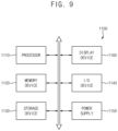
- FIG. 9 is a block diagram illustrating an electronic device including the display device of FIG. 1 .
- FIG. 1 is a block diagram illustrating a display device according to an embodiment.
- the display device 100 may include a display panel 110 including a plurality of pixels PX, a scan driver 120 that provides a scan signal SS to the plurality of pixels PX, a gamma reference generator 130 that generates a gamma reference voltages VGR, a data driver 140 that provides a data voltage VD to the plurality of pixels PX, and a controller 150 that controls the scan driver 120 , the gamma voltage generator 130 , and the data driver 140 .
- the display panel 110 may include a plurality of scan lines SL 1 to SLn, a plurality of data lines DL 1 to DLm, and a plurality of pixels PX (provided that n and m are integers greater than or equal to 2).
- Each of the scan lines SL 1 to SLn may extend in a first direction (e.g., a row direction), and each of the data lines DL 1 to DLm may extend in a second direction (e.g., a column direction) crossing the first direction.
- the scan lines SL 1 to SLn and the data lines DL 1 to DLm may be insulated from each other.
- the plurality of pixels PX may be arranged in a region where the scan lines SL 1 to SLn and the data lines DL 1 to DLm intersect.
- each of the plurality of pixels PX may include a switching transistor that transmits the data voltage VD in response to the scan signal SS, a storage capacitor that stores the data voltage VD transmitted by the switching transistor, a driving transistor that generates a driving current based on the data voltage VD stored in the storage capacitor, and a light emitting element that emits light based on the driving current generated by the driving transistor.
- the light emitting element may include a light emitting diode (LED), an organic light emitting diode (OLED), a quantum dot (QD) light emitting device, and the like.
- the scan driver 120 may provide the scan signals SS to the plurality of pixels PX through the plurality of scan lines SL 1 to SLn based on the scan control signal SCTRL received from the controller 150 .
- the scan driver 120 may sequentially provide the scan signals SS to the plurality of pixels PX in row units.
- the scan control signal SCTRL may include a scan start signal, a scan clock signal, and the like, but is not limited thereto.
- the scan driver 120 may be integrated or formed on the periphery of the display panel 110 .
- the scan driver 120 may be implemented with one or more integrated circuits (IC).
- the gamma voltage generator 130 may be controlled by a gamma control signal GCTRL from the controller 150 to generate one or more gamma reference voltages VGR.
- the gamma control signal GCTRL may indicate voltage levels of the gamma reference voltages VGR, and the gamma voltage generator 130 may be generate gamma reference voltages VGR corresponding to the voltage levels indicated by the gamma control signal GCTRL.
- the gamma voltage generator 130 may be included in the data driver 140 .
- the gamma voltage generator 130 may be located outside the data driver 140 .
- the data driver 140 may receive a data control signal DCTRL and an output image data ODAT from the controller 150 , may receive the gamma reference voltages VGR from the gamma voltage generator 130 , and may provide the data voltage VD to the plurality of pixels PX through the plurality of data line DL 1 to DLm based on the data control signal DCTRL, the output image data ODAT, and the gamma reference voltages VGR.
- the data driver 140 may generate respective grayscale voltages corresponding to each grayscale level based on the gamma reference voltages VGR, may select grayscale voltages corresponding to the output image data ODAT from among the grayscale voltages, and may provide the selected grayscale voltages as data voltages VD to the plurality of pixels PX.
- the data control signal DCTRL may include an output data enable signal, a horizontal start signal, a load signal, and the like, but is not limited thereto.
- the data driver 140 may be implemented as a single integrated circuit, and the integrated circuit may be referred to as a timing controller embedded data driver (TED).
- the data driver 140 may be implemented as separate integrated circuits.
- the controller 150 may receive the input image data IDAT and the control signal CTRL from an external host processor.
- the controller 150 may be a timing controller, and the host processor may be an application processor (AP), a graphic processing unit (GPU), or a graphic card.
- the input image data IDAT may be a RGB image data including red image data, green image data, and blue image data.
- the control signal CTRL may include a vertical synchronization signal, a horizontal synchronization signal, an input data enable signal, a master clock signal, and the like, but is not limited thereto.
- the controller 150 may generate the scan control signal SCTRL, the gamma control signal GCTRL, the data control signal DCTRL, and the output image data ODAT based on the input image data IDAT and the control signal CTRL.
- the controller 150 may control the operation of the scan driver 120 by providing the scan control signal SCTRL to the scan driver 120 , the operation of the gamma voltage generator 130 by providing the gamma control signal GCTRL to the gamma voltage generator 130 , the operation of the data driver 140 by providing the output image data ODAT and the data control signal DCTRL to the data driver 140 .
- the host processor may provide the input image data IDAT to the display device 100 at a variable input frame frequency (VIFF) (or variable frame rate) by changing a time length of a blank period for every frame period, and the controller 150 may receive the input image data IDAT from the host processor at the variable input frame frequency VIFF.
- VIFF variable input frame frequency
- the variable input frame frequency VIFF may be varied within a variable frequency range from a predetermined minimum frequency to a predetermined maximum frequency.
- the minimum frequency may be about 48 Hz
- the maximum frequency may be about 240 Hz
- the variable frequency range of the variable input frame frequency (VIFF) may be about 48 Hz to about 240 Hz, but is not limited thereto.
- the controller 150 may control the data driver 140 and the scan driver 130 to drive the display panel 110 at the variable input frequency (VIFF).
- VIFF variable input frequency
- a mode of the display device 100 in which the display panel 110 is driven at the variable input frame frequency VIFF may be referred to as a variable frame mode.
- the variable frame mode may be a free-sync mode, a mouse-sync mode, a Q-sync mode, or the like, but is not limited thereto.
- the controller 150 may include an image data processor 160 .
- the image data processor 160 may receive the input image data IDAT at the variable input frequency VIFF.
- the image data processor 160 may perform a luminance correction of the display panel 110 .
- the image data processor 160 may perform a color correction of the input image data IDAT.
- the image data processor 160 may be located an outside the controller 150 .
- FIG. 2 is a timing diagram illustrating an example of input image data input to the display device of FIG. 1 at a variable input frame frequency.
- a period or frequency of renderings 210 , 220 , and 230 of the host processor may not be constant, and the host processor may provide the input image data IDAT (that is, frame data FD1, FD2, and FD3) to the display device 100 in synchronization with a non-uniform period or frequency of the renderings 210 , 220 , and 230 in the variable frame mode.
- IDAT that is, frame data FD1, FD2, and FD3
- each frame period FP1, FP2, and FP3 has a constant active period AP1, AP2, and AP3 having a constant time length, but the host processor may provide frame data with the variable frame frequency VIFF to the display device 100 by changing a time length of the variable blank period VBP1, VBP2, and VBP3 of each frame period FP1, FP2, and FP3.
- the second frame data FD2 may be rendered 210 at a frequency of about 240 Hz, and at the same time, the host processor may provide previously rendered the first frame data FD1 at the variable input frame frequency VIFF of about 240 Hz to the display device 100 .
- the host processor may output the second frame data FD2 during the active period AP2 of the second frame period FP2 and may continue the variable blank period VBP2 of the second frame period FP2 until the rendering 200 of the third frame data FD3 is completed.
- the host processor may provide the second frame data FD2 at the variable input frame frequency VIFF of about 48 Hz by increasing the time of the variable blank period VBP2 of the second frame period FP2 in the display device 100 .
- the host processor may provide the third frame data FD3 back to the display device 100 at the variable input frame frequency VIFF of about 240 Hz.
- each of the frame periods FP1, FP2, and FP3 may include the active periods AP1, AP2, and AP3 having a constant time length regardless of the variable input frame frequency VIFF and the variable blank periods VBP1, VBP2, and VBP3 having a variable time length corresponding to the variable input frame frequency VIFF.
- the controller 150 may output the input image data IDAT received at the variable input frame frequency VIFF as the output image data ODAT to the data driver 140 at a driving frequency substantially equal to the variable input frame frequency VIFF.
- the display device 100 supporting the variable frame mode may display an image in synchronization with the variable input frame frequency VIFF, thereby preventing a tearing phenomenon caused by frame frequency mismatch.
- the luminance of the display panel 110 may be changed according to the variable input frame frequency VIFF, that is, the driving frequency of the display panel 100 .
- the number of times each pixel PX of the display panel 110 driven at a first driving frequency is initialized may be different from the number of times the display panel 110 driven at a second driving frequency different from the first driving frequency is initialized during the same time period. Accordingly, the luminance of the display panel 110 driven at the first driving frequency may be different from the luminance of the display panel 110 driven at the second driving frequency.
- FIG. 3 is a diagram illustrating an example of the luminance of a display panel driven at different frame frequencies when luminance correction is not performed.
- FIG. 3 shows an example of the luminance 310 of the display panel 110 driven at a first driving frequency of about 48 Hz and an example of the luminance 330 of the display panel 110 driven at second driving frequency of about 240 Hz in the variable frame mode.
- each pixel PX of the display panel 100 driven at the first driving frequency of about 48 Hz may be initialized about 2.5 times and each pixel PX of the display panel 100 driven at the second driving frequency of about 240 Hz may be turned off about 13 times. Accordingly, an average luminance AVGLUM2 of the display panel 110 driven with the second driving frequency of about 240 Hz may be lower than an average luminance AVGLUM1 of the display panel 110 driven with the first driving frequency of about 48 Hz.
- the display device 100 may perform the luminance correction according to the variable input frame frequency VIFF to remove or reduce the difference in luminance of the display panel 110 according to the variable input frame frequency VIFF, that is, the driving frequency of the display panel 110 .
- FIG. 4 is a diagram illustrating an example of the luminance of a display panel when luminance correction is not performed ( 350 ) and an example of the luminance of a display panel when luminance correction is performed ( 370 ).
- the luminance of the display panel 110 driven at the variable input frame frequency VIFF of about 240 Hz may be different from the luminance of the display panel 110 driven with the variable input frame frequency VIFF of about 120 Hz.
- the luminance of the display panel 110 driven at a variable input frame frequency VIFF of about 240 Hz and the luminance of the display panel 110 driven with the variable input frame frequency VIFF of about 120 Hz may be similar to each other.
- the display device 100 may determine the minimum frequency in the variable frequency range of the variable input frame frequency VIFF as a reference frequency, may determine the luminance of the display panel 110 at the reference frequency as a reference luminance, and may perform the luminance correction based on the reference luminance corresponding to the reference frequency.
- FIG. 5 is a diagram illustrating an example of a color coordinate value according to the luminance of a display panel.
- a color coordinate value may vary according to the luminance of the display panel 110 .
- the color coordinate value may vary according to the luminance of the display panel 110 in a low luminance region having a luminance range of about 0.5 nit or less. That is, when the luminance correction is performed, the color coordinate value may change according to the luminance of the display panel 110 in the low luminance region. In addition, even when the luminance is the same, the color coordinate value change may occur. In this case, the color coordinate value change may be recognized as the flicker.
- the image data processor 160 of the controller 150 may perform the luminance correction and the color correction. That is, the image data processor 160 of the controller 150 may determine a first correction value for correcting a luminance of the display panel 110 according to the variable input frame frequency VIFF, may determine a second correction value for correcting color coordinate values for components of the input image date IDAT to which the first correction value is reflected, and may output the output image date ODAT obtained by adding the input image data IDAT to which the first correction value is reflected and the second correction value. Accordingly, the flicker when the variable input frame frequency VIFF is changed can be minimized or reduced.
- the image data processor 160 of the controller 150 may determine the first correction value for correcting a luminance of the display panel 110 according to the variable input frame frequency VIFF, may determine whether the luminance of the display panel 110 falls in any luminance range of a first luminance range and a second luminance range, may determine the second correction value for correcting color coordinate values of RGB components of the input image data IDAT to which the first correction value is reflected when the luminance of the display panel 110 falls in the first luminance range, and may output the output image date ODAT obtained by adding the input image data IDAT to which the first correction value is reflected and the second correction value.
- the image data processor 160 of the controller 150 may determine the output image data ODAT obtained by adding the input image data IDAT and the first correction value when the luminance of the display panel 110 falls within the second luminance.
- the first luminance range may be from about 0.5 nit to about 4.5 nit
- the second luminance range may be less than about 0.5 nit and greater than about 4.5 nit.
- FIG. 6 is a block diagram illustrating the image data processor of FIG. 1 .
- the image data processor 160 of the controller 150 may include a first correction value determiner 410 , a second correction value determiner 420 , and an image data corrector 430 .
- the first correction value determiner 410 may include a first lookup table 511 , a second lookup table 512 , and a third lookup table 513 .
- Each of the first lookup table 511 , the second lookup table 512 , and the third lookup table 513 may respectively correspond to the variable input frame frequency VIFF and store the different first correction values.
- the first lookup table 511 may correspond to the variable input frame frequency VIFF of about 144 Hz
- the second lookup table 512 may correspond to the variable input frame frequency VIFF of about 120 Hz
- the third lookup table 513 may correspond to the variable input frame frequency VIFF of about 48 Hz.
- the first correction value determiner 410 may select one lookup table corresponding to the variable input frame frequency VIFF from among the first lookup table 511 , the second lookup table 512 , and the third lookup table 513 .
- the first correction value determiner 410 may determine the first correction value for correcting the input image data IDAT by referring to the selected lookup table.
- the first correction value may be reflected in the input image data IDAT.
- the second correction value determiner 420 may determine the second correction value for correcting the color coordinate value of the input image data IDAT to which the first correction value is reflected. That is, the second correction value determiner 420 may determine the degree of color correction of the input image data IDAT to which the first correction value is reflected.
- the second correction value determiner 420 may determine a color coordinate value corrected for any one of the RGB components of the input image data IDAT to which the first correction value is reflected.
- the second correction value determiner 420 first determines the color coordinate values corrected for the B component, but the present disclosure is not limited thereto.
- the present disclosure can be applied to a case in which color coordinate values corrected for an R component or a G component are first determined.
- the second correction value determiner 420 may determine the corrected color coordinate values of the remaining components based on the corrected color coordinate values of the B component.
- a method of determining the corrected color coordinate values of other components (e.g., the R component and the G component) based on the predetermined corrected color coordinate values of any one component (e.g., the B component) will be described below in detail.
- the second correction value determiner 420 may correct the color coordinate values of the other components in response to a correction ratio of the corrected color coordinate values for any one component. If the color coordinate values of the original RGB components are R o , G o , and B o , and the ratio of the corrected color coordinate values to the original color coordinate values of the B component is I reduce (%), the corrected color coordinates values of R r , G r , and B r for the corrected RGB components are expressed in Equation 1 below.
- the second correction value determiner 420 may determine the corrected color coordinate values of other components by using a color space conversion.
- the second correction value determiner 420 may convert the RGB color coordinate values of the input image data IDAT into color coordinate values of a Lab color space.
- the Lab color space may be divided into coordinate values for the “L” component, the “a” component, and the “b” component.
- the “L” component may represent the brightness of a color (e.g., 0 is black, 100 is white).
- the “a” component is chromaticity, and a positive number may indicate red and a negative number may indicate green.
- the “b” component is chromaticity, and a positive number may represent blue and a negative number may represent yellow.
- the second correction value determiner 420 may convert the RGB color coordinate values into the color coordinate values of the XYZ color space through Equation 2 below using a preset transformation matrix M.
- the converted color coordinate values of the XYZ color space may be converted back into color coordinate values of the Lab color space according to Equation 3 below.
- the second correction value determiner 420 may determine the color coordinate values of the other components such that the Lab color difference between the input image data IDAT to which the first correction value is reflected and the output image data, that is, the distance between the Lab color coordinates is minimized based on the corrected color coordinate value of the “B” component.
- the Lab color difference may be defined as in Equation 4 below.
- W is the color difference
- L o , a o , and b o are Lab color coordinate values for the input image data IDAT to which the first correction value is reflected
- L r , a r , and b r are Lab color coordinate values for the output image data ODAT.
- W ⁇ square root over (
- the “Z” component in the XYZ color space is determined by 0.0193R+0.1192G+0.9503B, the “Z” component may be approximated to the “B” component in the RGB color space.
- the second correction value determiner 420 may determine a fixed value by approximating the Z value based on the predetermined corrected color coordinate value of the B component.
- the second correction value determiner 420 may determine the X and Y values to minimize the color difference between the input image data IDAT to which the first correction value is reflected and the output image data ODAT. From the Equation 4, the X and Y values may be determined by Equations 5 and 6 below. In Equations 5 and 6, X o , Y o , and Z o are XYZ color coordinate values for the input image data IDAT to which the first correction value is reflected, and X r , Y r , and Z r are XYZ color coordinate values for the output image data ODAT.
- the Z r is a predetermined value based on the corrected color coordinate value of the “B” component as described above.
- X r [ ( X n Z n ) 1 / 3 ⁇ 200 2 100 2 + 200 2 ⁇ ( Z r 1 / 3 - Z 0 1 / 3 ) + X 0 1 / 3 ] 3 [ Equation ⁇ 5 ]
- Y r [ ( Y n Z n ) 1 / 3 ⁇ 200 2 100 2 + 200 2 ⁇ ( Z r 1 / 3 - Z 0 1 / 3 ) + Y 0 1 / 3 ] 3 [ Equation ⁇ 6 ]
- the second correction value determiner 420 may determine the corrected color coordinate values of the RGB components by inversely calculating the Equation 2 based on X r , Y r , and predetermined Z r values determined by the Equations 5 and 6.
- the RGB color coordinate values inversely calculated from the X r , Y r , and Z r values may be expressed as in Equation 7 below.
- R′, G′, and B′ are color coordinate values of the finally corrected RGB components.
- the corrected color coordinate value of the “B” component determined by the Equation 7 may be different from the predetermined corrected color coordinate value of the “B” component, but an error therebetween may not be large. Accordingly, the second correction value determiner 420 may select the predetermined corrected color coordinate value of the “B” component or may select the corrected color coordinate value of the “B” component determined by the Equation 7.
- the second correction value determiner 420 uses the Lab color space conversion, but the present disclosure is not limited thereto.
- the second correction value determiner 420 may use conversion into various color spaces such as an u′v′ color space, a CIE2001 color space, or the like.
- the image data corrector 430 may correct the input image data IDAT to which the first correction value is reflected by applying the corrected color coordinate values (i.e., the second correction value) of the RGB components determined by the second correction value determiner 420 .
- the image data corrector 430 may output the output image date ODAT obtained by adding the input image data IDAT to which the first correction value is reflected and the second correction value.
- FIG. 7 is a flowchart illustrating a method of driving a display device according to an embodiment.
- the image data processor 160 of the controller 150 may receive the input image data IDAT at the variable input frame frequency VIFF (S 110 ).
- the controller 150 may check the luminance of the display panel 110 based on the input image data IDAT (S 120 ).
- the controller 150 may sense the variable input frame frequency VIFF based on the luminance of the display panel 110 (S 130 ). That is, after the luminance of the display panel 110 is checked, the variable input frame frequency VIFF may be sensed based on the checked luminance of the display panel 110 .
- the image data processor 160 of the controller 150 may determine the first correction value for correcting the luminance of the display panel 110 according to the variable input frame frequency VIFF (S 140 ). Specifically, the image data processor 160 of the controller 150 may determine the minimum frequency in the variable frequency range of the variable input frame frequency VIFF as the reference frequency, may determine the reference luminance as the luminance of the display panel 110 at the reference frequency, and may determine the first correction value based on the reference luminance corresponding to the reference frequency.
- the image data processor 160 of the controller 150 may determine the second correction value for correcting the color coordinate values of the RGB components of the input image data IDAT to which the first correction value is reflected (S 150 ). A detailed description of the method of determining the second correction value is the same as described above. Lastly, the image data processor 160 of the controller 150 may output the output image date ODAT obtained by adding the input image data IDAT to which the first correction value is reflected and the second correction value (S 160 ).
- FIG. 8 is a flowchart illustrating a method of driving a display device according to another embodiment.
- a configuration that is the same as or similar to the driving method of the display device 100 described with reference to FIG. 8 will be omitted or briefly described.
- the image data processor 160 of the controller 150 may receive input image data IDAT at the variable input frame frequency VIFF (S 210 ).
- the controller 150 may check the luminance of the display panel 110 based on the input image data IDAT (S 220 ).
- the controller 150 may sense the variable input frame frequency VIFF based on the luminance of the display panel 110 (S 230 ).
- the image data processor 160 of the controller 150 may determine the first correction value for correcting the luminance of the display panel 110 according to the variable input frame frequency VIFF (S 240 ).
- the image data processor 160 of the controller 150 may determine whether the luminance of the display panel 110 is within the first luminance range (S 250 ). Specifically, for each pixel PX of the display panel 110 , the image data processor 160 of the controller 150 may determine whether the luminance of the display panel 110 is within any luminance range of the first luminance range and the second luminance range.
- the first luminance range may be from about 0.5 nit to about 4.5 nit
- the second luminance range may be less than about 0.5 nit and greater than about 4.5 nit.
- the image data processor 160 of the controller 150 may determine the second correction value for correcting color coordinate values of the RGB components of the input image data IDAT to which the first correction value is reflected (S 260 ). Thereafter, the image data processor 160 of the controller 150 may output the output image date ODAT obtained by adding the input image data IDAT to which the first correction value is reflected and the second correction value (S 270 ).
- the image data processor 160 of the controller 150 may output the output image date ODAT obtained by adding the input image data IDAT and the first correction value (S 280 ). That is, the image data processor 160 of the controller 150 may not perform color correction on the input image data IDAT.
- FIG. 9 is a block diagram illustrating an electronic device including the display device of FIG. 1 .
- the display device 1160 shown in FIG. 9 may correspond to the display device 100 shown in FIG. 1 .
- the electronic device 1100 may include a processor 1110 , a memory device 1120 , a storage device 1130 , an input/output (I/O) device 1140 , a power supply 1150 , and the display device 1160 .
- the electronic device 1100 may further include a plurality of ports for communicating with a video card, a sound card, a memory card, a universal serial bus (USB) device, other electronic devices, and the like.
- USB universal serial bus
- the processor 1110 may perform various computing functions or tasks.
- the processor 1110 may be an application processor (AP), a microprocessor, a central processing unit (CPU), etc.
- the processor 1110 may be coupled to other components via an address bus, a control bus, a data bus, etc. Further, in some embodiments, the processor 1110 may be further coupled to an extended bus such as a peripheral component interconnection (PCI) bus.
- PCI peripheral component interconnection
- the memory device 1120 may store data for operations of the electronic device 1100 .
- the memory device 1120 may include at least one non-volatile memory device such as an erasable programmable read-only memory (EPROM) device, an electrically erasable programmable read-only memory (EEPROM) device, a flash memory device, a phase change random access memory (PRAM) device, a resistance random access memory (RRAM) device, a nano floating gate memory (NFGM) device, a polymer random access memory (PoRAM) device, a magnetic random access memory (MRAM) device, a ferroelectric random access memory (FRAM) device, and the like, and/or at least one volatile memory device such as a dynamic random access memory (DRAM) device, a static random access memory (SRAM) device, a mobile dynamic random access memory (mobile DRAM) device, and the like.
- DRAM dynamic random access memory
- SRAM static random access memory
- mobile DRAM mobile dynamic random access memory
- the storage device 1130 may be a solid state drive (SSD) device, a hard disk drive (HDD) device, a CD-ROM device, etc.
- the I/O device 1140 may be an input device such as a keyboard, a keypad, a mouse, a touch screen, and the like, and an output device such as a printer, a speaker, and the like.
- the power supply 1150 may supply power for operations of the electronic device 1100 .
- the display device 1160 may be coupled to other components through the buses or other communication links.
- the electronic device 1100 may be nay electronic device including the display device 160 such as a smart phone, a mobile phone, a tablet computer, a digital TV, a 3D TV, a personal computer (PC), a home electronic device, a laptop computer, a personal digital assistants (PDA), a portable multimedia player (PMPs), a digital camera, a music player, a portable game console, a navigation, and the like.
- the display device 160 such as a smart phone, a mobile phone, a tablet computer, a digital TV, a 3D TV, a personal computer (PC), a home electronic device, a laptop computer, a personal digital assistants (PDA), a portable multimedia player (PMPs), a digital camera, a music player, a portable game console, a navigation, and the like.
- the display device 160 such as a smart phone, a mobile phone, a tablet computer, a digital TV, a 3D TV, a personal computer (PC), a home electronic device, a laptop
- the present disclosure can be applied to various display devices.
- the present disclosure is applicable to various display devices such as display devices for vehicles, ships and aircraft, portable communication devices, display devices for exhibition or information transmission, medical display devices, and the like.
Landscapes
- Engineering & Computer Science (AREA)
- Physics & Mathematics (AREA)
- Computer Hardware Design (AREA)
- General Physics & Mathematics (AREA)
- Theoretical Computer Science (AREA)
- Multimedia (AREA)
- Signal Processing (AREA)
- Control Of Indicators Other Than Cathode Ray Tubes (AREA)
Abstract
Description
W=√{square root over (|L o −L r|2 +|a o −a r|2 +|b o −b r|2)}
Claims (20)
Applications Claiming Priority (2)
| Application Number | Priority Date | Filing Date | Title |
|---|---|---|---|
| KR10-2022-0031007 | 2022-03-11 | ||
| KR1020220031007A KR20230134068A (en) | 2022-03-11 | 2022-03-11 | Display device and method of operating the same |
Publications (2)
| Publication Number | Publication Date |
|---|---|
| US20230290314A1 US20230290314A1 (en) | 2023-09-14 |
| US12148395B2 true US12148395B2 (en) | 2024-11-19 |
Family
ID=87910281
Family Applications (1)
| Application Number | Title | Priority Date | Filing Date |
|---|---|---|---|
| US18/102,794 Active 2043-02-11 US12148395B2 (en) | 2022-03-11 | 2023-01-30 | Display device and method of operating the same |
Country Status (3)
| Country | Link |
|---|---|
| US (1) | US12148395B2 (en) |
| KR (1) | KR20230134068A (en) |
| CN (1) | CN116741088A (en) |
Citations (3)
| Publication number | Priority date | Publication date | Assignee | Title |
|---|---|---|---|---|
| CN110060642A (en) | 2018-01-19 | 2019-07-26 | 三星显示有限公司 | Receiving device and liquid crystal display including receiving device |
| US10839755B2 (en) | 2017-12-11 | 2020-11-17 | Samsung Display Co., Ltd. | Display device capable of changing luminance depending on operating frequency |
| US20230162648A1 (en) * | 2020-03-24 | 2023-05-25 | Iix Inc. | Input signal correction device |
-
2022
- 2022-03-11 KR KR1020220031007A patent/KR20230134068A/en active Pending
- 2022-11-21 CN CN202211451906.6A patent/CN116741088A/en active Pending
-
2023
- 2023-01-30 US US18/102,794 patent/US12148395B2/en active Active
Patent Citations (4)
| Publication number | Priority date | Publication date | Assignee | Title |
|---|---|---|---|---|
| US10839755B2 (en) | 2017-12-11 | 2020-11-17 | Samsung Display Co., Ltd. | Display device capable of changing luminance depending on operating frequency |
| CN110060642A (en) | 2018-01-19 | 2019-07-26 | 三星显示有限公司 | Receiving device and liquid crystal display including receiving device |
| US10902817B2 (en) | 2018-01-19 | 2021-01-26 | Samsung Display Co., Ltd. | Sink device with variable frame rate and liquid crystal display device including the same |
| US20230162648A1 (en) * | 2020-03-24 | 2023-05-25 | Iix Inc. | Input signal correction device |
Also Published As
| Publication number | Publication date |
|---|---|
| CN116741088A (en) | 2023-09-12 |
| US20230290314A1 (en) | 2023-09-14 |
| KR20230134068A (en) | 2023-09-20 |
Similar Documents
| Publication | Publication Date | Title |
|---|---|---|
| US12283252B2 (en) | Display device and method of driving display device | |
| US11488524B2 (en) | Organic light emitting diode display device, and method of operating an organic light emitting diode display device | |
| US11151928B2 (en) | Flexible display device, and method of operating a flexible display device | |
| US11289029B1 (en) | Organic light emitting diode display device, and method of operating an organic light emitting diode display device | |
| US11227555B2 (en) | Display device performing adaptive refresh | |
| US20260045198A1 (en) | Display device, method of driving the same, and electronic device including the same | |
| US12380840B2 (en) | Display device and method of generating temperature profile of display device | |
| US12106720B2 (en) | Display device and method of operating the display device | |
| US12118950B2 (en) | Display device, and method of operating a display device | |
| US12300147B2 (en) | Display device performing a dummy scan operation | |
| US12039910B2 (en) | Display device | |
| US11257412B2 (en) | Display device performing peak luminance driving, and method of operating a display device | |
| US12148395B2 (en) | Display device and method of operating the same | |
| US11817031B2 (en) | Display device and method of operating the same | |
| US12451085B2 (en) | Display device and method of driving the same | |
| US12525175B2 (en) | Display device and method for driving the same | |
| US11967262B2 (en) | Display device compensating for light stress | |
| US12217643B2 (en) | Display device and method of driving the same | |
| US12057057B2 (en) | Display device | |
| KR102926721B1 (en) | Display device and method of operating the same | |
| US20250104611A1 (en) | Display device and method of driving the same | |
| US20260031023A1 (en) | Display device and electronic device including the display device | |
| KR20260004611A (en) | Display device and method of compensating for luminance and color of display device |
Legal Events
| Date | Code | Title | Description |
|---|---|---|---|
| FEPP | Fee payment procedure |
Free format text: ENTITY STATUS SET TO UNDISCOUNTED (ORIGINAL EVENT CODE: BIG.); ENTITY STATUS OF PATENT OWNER: LARGE ENTITY |
|
| AS | Assignment |
Owner name: SAMSUNG DISPLAY CO., LTD., KOREA, REPUBLIC OF Free format text: ASSIGNMENT OF ASSIGNORS INTEREST;ASSIGNOR:LEE, KYUNG-HUN;REEL/FRAME:062538/0637 Effective date: 20221228 |
|
| STPP | Information on status: patent application and granting procedure in general |
Free format text: DOCKETED NEW CASE - READY FOR EXAMINATION |
|
| STPP | Information on status: patent application and granting procedure in general |
Free format text: NON FINAL ACTION MAILED |
|
| STPP | Information on status: patent application and granting procedure in general |
Free format text: RESPONSE TO NON-FINAL OFFICE ACTION ENTERED AND FORWARDED TO EXAMINER |
|
| STPP | Information on status: patent application and granting procedure in general |
Free format text: NOTICE OF ALLOWANCE MAILED -- APPLICATION RECEIVED IN OFFICE OF PUBLICATIONS |
|
| STPP | Information on status: patent application and granting procedure in general |
Free format text: PUBLICATIONS -- ISSUE FEE PAYMENT VERIFIED |
|
| STCF | Information on status: patent grant |
Free format text: PATENTED CASE |