US12142544B2 - Semiconductor package - Google Patents
Semiconductor package Download PDFInfo
- Publication number
- US12142544B2 US12142544B2 US17/734,700 US202217734700A US12142544B2 US 12142544 B2 US12142544 B2 US 12142544B2 US 202217734700 A US202217734700 A US 202217734700A US 12142544 B2 US12142544 B2 US 12142544B2
- Authority
- US
- United States
- Prior art keywords
- pads
- pad group
- semiconductor
- connection terminal
- semiconductor chip
- Prior art date
- Legal status (The legal status is an assumption and is not a legal conclusion. Google has not performed a legal analysis and makes no representation as to the accuracy of the status listed.)
- Active, expires
Links
Images


Classifications
-
- H—ELECTRICITY
- H01—ELECTRIC ELEMENTS
- H01L—SEMICONDUCTOR DEVICES NOT COVERED BY CLASS H10
- H01L23/00—Details of semiconductor or other solid state devices
- H01L23/48—Arrangements for conducting electric current to or from the solid state body in operation, e.g. leads, terminal arrangements ; Selection of materials therefor
- H01L23/481—Internal lead connections, e.g. via connections, feedthrough structures
-
- H10W20/40—
-
- H—ELECTRICITY
- H01—ELECTRIC ELEMENTS
- H01L—SEMICONDUCTOR DEVICES NOT COVERED BY CLASS H10
- H01L24/00—Arrangements for connecting or disconnecting semiconductor or solid-state bodies; Methods or apparatus related thereto
- H01L24/01—Means for bonding being attached to, or being formed on, the surface to be connected, e.g. chip-to-package, die-attach, "first-level" interconnects; Manufacturing methods related thereto
- H01L24/02—Bonding areas ; Manufacturing methods related thereto
- H01L24/07—Structure, shape, material or disposition of the bonding areas after the connecting process
- H01L24/08—Structure, shape, material or disposition of the bonding areas after the connecting process of an individual bonding area
-
- H—ELECTRICITY
- H01—ELECTRIC ELEMENTS
- H01L—SEMICONDUCTOR DEVICES NOT COVERED BY CLASS H10
- H01L24/00—Arrangements for connecting or disconnecting semiconductor or solid-state bodies; Methods or apparatus related thereto
- H01L24/01—Means for bonding being attached to, or being formed on, the surface to be connected, e.g. chip-to-package, die-attach, "first-level" interconnects; Manufacturing methods related thereto
- H01L24/02—Bonding areas ; Manufacturing methods related thereto
- H01L24/07—Structure, shape, material or disposition of the bonding areas after the connecting process
- H01L24/09—Structure, shape, material or disposition of the bonding areas after the connecting process of a plurality of bonding areas
-
- H—ELECTRICITY
- H01—ELECTRIC ELEMENTS
- H01L—SEMICONDUCTOR DEVICES NOT COVERED BY CLASS H10
- H01L24/00—Arrangements for connecting or disconnecting semiconductor or solid-state bodies; Methods or apparatus related thereto
- H01L24/01—Means for bonding being attached to, or being formed on, the surface to be connected, e.g. chip-to-package, die-attach, "first-level" interconnects; Manufacturing methods related thereto
- H01L24/10—Bump connectors ; Manufacturing methods related thereto
- H01L24/15—Structure, shape, material or disposition of the bump connectors after the connecting process
- H01L24/16—Structure, shape, material or disposition of the bump connectors after the connecting process of an individual bump connector
-
- H—ELECTRICITY
- H01—ELECTRIC ELEMENTS
- H01L—SEMICONDUCTOR DEVICES NOT COVERED BY CLASS H10
- H01L24/00—Arrangements for connecting or disconnecting semiconductor or solid-state bodies; Methods or apparatus related thereto
- H01L24/01—Means for bonding being attached to, or being formed on, the surface to be connected, e.g. chip-to-package, die-attach, "first-level" interconnects; Manufacturing methods related thereto
- H01L24/10—Bump connectors ; Manufacturing methods related thereto
- H01L24/15—Structure, shape, material or disposition of the bump connectors after the connecting process
- H01L24/17—Structure, shape, material or disposition of the bump connectors after the connecting process of a plurality of bump connectors
-
- H—ELECTRICITY
- H01—ELECTRIC ELEMENTS
- H01L—SEMICONDUCTOR DEVICES NOT COVERED BY CLASS H10
- H01L25/00—Assemblies consisting of a plurality of semiconductor or other solid state devices
- H01L25/03—Assemblies consisting of a plurality of semiconductor or other solid state devices all the devices being of a type provided for in a single subclass of subclasses H10B, H10D, H10F, H10H, H10K or H10N, e.g. assemblies of rectifier diodes
- H01L25/04—Assemblies consisting of a plurality of semiconductor or other solid state devices all the devices being of a type provided for in a single subclass of subclasses H10B, H10D, H10F, H10H, H10K or H10N, e.g. assemblies of rectifier diodes the devices not having separate containers
- H01L25/065—Assemblies consisting of a plurality of semiconductor or other solid state devices all the devices being of a type provided for in a single subclass of subclasses H10B, H10D, H10F, H10H, H10K or H10N, e.g. assemblies of rectifier diodes the devices not having separate containers the devices being of a type provided for in group H10D89/00
- H01L25/0657—Stacked arrangements of devices
-
- H10W80/00—
-
- H10W90/00—
-
- H—ELECTRICITY
- H01—ELECTRIC ELEMENTS
- H01L—SEMICONDUCTOR DEVICES NOT COVERED BY CLASS H10
- H01L2224/00—Indexing scheme for arrangements for connecting or disconnecting semiconductor or solid-state bodies and methods related thereto as covered by H01L24/00
- H01L2224/01—Means for bonding being attached to, or being formed on, the surface to be connected, e.g. chip-to-package, die-attach, "first-level" interconnects; Manufacturing methods related thereto
- H01L2224/02—Bonding areas; Manufacturing methods related thereto
- H01L2224/07—Structure, shape, material or disposition of the bonding areas after the connecting process
- H01L2224/08—Structure, shape, material or disposition of the bonding areas after the connecting process of an individual bonding area
- H01L2224/0801—Structure
-
- H—ELECTRICITY
- H01—ELECTRIC ELEMENTS
- H01L—SEMICONDUCTOR DEVICES NOT COVERED BY CLASS H10
- H01L2224/00—Indexing scheme for arrangements for connecting or disconnecting semiconductor or solid-state bodies and methods related thereto as covered by H01L24/00
- H01L2224/01—Means for bonding being attached to, or being formed on, the surface to be connected, e.g. chip-to-package, die-attach, "first-level" interconnects; Manufacturing methods related thereto
- H01L2224/02—Bonding areas; Manufacturing methods related thereto
- H01L2224/07—Structure, shape, material or disposition of the bonding areas after the connecting process
- H01L2224/08—Structure, shape, material or disposition of the bonding areas after the connecting process of an individual bonding area
- H01L2224/0805—Shape
- H01L2224/08057—Shape in side view
- H01L2224/08058—Shape in side view being non uniform along the bonding area
-
- H—ELECTRICITY
- H01—ELECTRIC ELEMENTS
- H01L—SEMICONDUCTOR DEVICES NOT COVERED BY CLASS H10
- H01L2224/00—Indexing scheme for arrangements for connecting or disconnecting semiconductor or solid-state bodies and methods related thereto as covered by H01L24/00
- H01L2224/01—Means for bonding being attached to, or being formed on, the surface to be connected, e.g. chip-to-package, die-attach, "first-level" interconnects; Manufacturing methods related thereto
- H01L2224/02—Bonding areas; Manufacturing methods related thereto
- H01L2224/07—Structure, shape, material or disposition of the bonding areas after the connecting process
- H01L2224/08—Structure, shape, material or disposition of the bonding areas after the connecting process of an individual bonding area
- H01L2224/081—Disposition
- H01L2224/0812—Disposition the bonding area connecting directly to another bonding area, i.e. connectorless bonding, e.g. bumpless bonding
- H01L2224/08135—Disposition the bonding area connecting directly to another bonding area, i.e. connectorless bonding, e.g. bumpless bonding the bonding area connecting between different semiconductor or solid-state bodies, i.e. chip-to-chip
- H01L2224/08145—Disposition the bonding area connecting directly to another bonding area, i.e. connectorless bonding, e.g. bumpless bonding the bonding area connecting between different semiconductor or solid-state bodies, i.e. chip-to-chip the bodies being stacked
- H01L2224/08148—Disposition the bonding area connecting directly to another bonding area, i.e. connectorless bonding, e.g. bumpless bonding the bonding area connecting between different semiconductor or solid-state bodies, i.e. chip-to-chip the bodies being stacked the bonding area connecting to a bonding area protruding from the surface of the body
-
- H—ELECTRICITY
- H01—ELECTRIC ELEMENTS
- H01L—SEMICONDUCTOR DEVICES NOT COVERED BY CLASS H10
- H01L2224/00—Indexing scheme for arrangements for connecting or disconnecting semiconductor or solid-state bodies and methods related thereto as covered by H01L24/00
- H01L2224/01—Means for bonding being attached to, or being formed on, the surface to be connected, e.g. chip-to-package, die-attach, "first-level" interconnects; Manufacturing methods related thereto
- H01L2224/02—Bonding areas; Manufacturing methods related thereto
- H01L2224/07—Structure, shape, material or disposition of the bonding areas after the connecting process
- H01L2224/09—Structure, shape, material or disposition of the bonding areas after the connecting process of a plurality of bonding areas
- H01L2224/0901—Structure
- H01L2224/0903—Bonding areas having different sizes, e.g. different diameters, heights or widths
-
- H—ELECTRICITY
- H01—ELECTRIC ELEMENTS
- H01L—SEMICONDUCTOR DEVICES NOT COVERED BY CLASS H10
- H01L2224/00—Indexing scheme for arrangements for connecting or disconnecting semiconductor or solid-state bodies and methods related thereto as covered by H01L24/00
- H01L2224/01—Means for bonding being attached to, or being formed on, the surface to be connected, e.g. chip-to-package, die-attach, "first-level" interconnects; Manufacturing methods related thereto
- H01L2224/02—Bonding areas; Manufacturing methods related thereto
- H01L2224/07—Structure, shape, material or disposition of the bonding areas after the connecting process
- H01L2224/09—Structure, shape, material or disposition of the bonding areas after the connecting process of a plurality of bonding areas
- H01L2224/091—Disposition
- H01L2224/0912—Layout
- H01L2224/0913—Square or rectangular array
- H01L2224/09132—Square or rectangular array being non uniform, i.e. having a non uniform pitch across the array
-
- H—ELECTRICITY
- H01—ELECTRIC ELEMENTS
- H01L—SEMICONDUCTOR DEVICES NOT COVERED BY CLASS H10
- H01L2224/00—Indexing scheme for arrangements for connecting or disconnecting semiconductor or solid-state bodies and methods related thereto as covered by H01L24/00
- H01L2224/01—Means for bonding being attached to, or being formed on, the surface to be connected, e.g. chip-to-package, die-attach, "first-level" interconnects; Manufacturing methods related thereto
- H01L2224/02—Bonding areas; Manufacturing methods related thereto
- H01L2224/07—Structure, shape, material or disposition of the bonding areas after the connecting process
- H01L2224/09—Structure, shape, material or disposition of the bonding areas after the connecting process of a plurality of bonding areas
- H01L2224/091—Disposition
- H01L2224/0912—Layout
- H01L2224/0913—Square or rectangular array
- H01L2224/09133—Square or rectangular array with a staggered arrangement, e.g. depopulated array
-
- H—ELECTRICITY
- H01—ELECTRIC ELEMENTS
- H01L—SEMICONDUCTOR DEVICES NOT COVERED BY CLASS H10
- H01L2224/00—Indexing scheme for arrangements for connecting or disconnecting semiconductor or solid-state bodies and methods related thereto as covered by H01L24/00
- H01L2224/01—Means for bonding being attached to, or being formed on, the surface to be connected, e.g. chip-to-package, die-attach, "first-level" interconnects; Manufacturing methods related thereto
- H01L2224/10—Bump connectors; Manufacturing methods related thereto
- H01L2224/15—Structure, shape, material or disposition of the bump connectors after the connecting process
- H01L2224/16—Structure, shape, material or disposition of the bump connectors after the connecting process of an individual bump connector
- H01L2224/1601—Structure
- H01L2224/16012—Structure relative to the bonding area, e.g. bond pad
- H01L2224/16013—Structure relative to the bonding area, e.g. bond pad the bump connector being larger than the bonding area, e.g. bond pad
-
- H—ELECTRICITY
- H01—ELECTRIC ELEMENTS
- H01L—SEMICONDUCTOR DEVICES NOT COVERED BY CLASS H10
- H01L2224/00—Indexing scheme for arrangements for connecting or disconnecting semiconductor or solid-state bodies and methods related thereto as covered by H01L24/00
- H01L2224/01—Means for bonding being attached to, or being formed on, the surface to be connected, e.g. chip-to-package, die-attach, "first-level" interconnects; Manufacturing methods related thereto
- H01L2224/10—Bump connectors; Manufacturing methods related thereto
- H01L2224/15—Structure, shape, material or disposition of the bump connectors after the connecting process
- H01L2224/16—Structure, shape, material or disposition of the bump connectors after the connecting process of an individual bump connector
- H01L2224/1601—Structure
- H01L2224/16012—Structure relative to the bonding area, e.g. bond pad
- H01L2224/16014—Structure relative to the bonding area, e.g. bond pad the bump connector being smaller than the bonding area, e.g. bond pad
-
- H—ELECTRICITY
- H01—ELECTRIC ELEMENTS
- H01L—SEMICONDUCTOR DEVICES NOT COVERED BY CLASS H10
- H01L2224/00—Indexing scheme for arrangements for connecting or disconnecting semiconductor or solid-state bodies and methods related thereto as covered by H01L24/00
- H01L2224/01—Means for bonding being attached to, or being formed on, the surface to be connected, e.g. chip-to-package, die-attach, "first-level" interconnects; Manufacturing methods related thereto
- H01L2224/10—Bump connectors; Manufacturing methods related thereto
- H01L2224/15—Structure, shape, material or disposition of the bump connectors after the connecting process
- H01L2224/16—Structure, shape, material or disposition of the bump connectors after the connecting process of an individual bump connector
- H01L2224/1605—Shape
- H01L2224/16052—Shape in top view
- H01L2224/16055—Shape in top view being circular or elliptic
-
- H—ELECTRICITY
- H01—ELECTRIC ELEMENTS
- H01L—SEMICONDUCTOR DEVICES NOT COVERED BY CLASS H10
- H01L2224/00—Indexing scheme for arrangements for connecting or disconnecting semiconductor or solid-state bodies and methods related thereto as covered by H01L24/00
- H01L2224/01—Means for bonding being attached to, or being formed on, the surface to be connected, e.g. chip-to-package, die-attach, "first-level" interconnects; Manufacturing methods related thereto
- H01L2224/10—Bump connectors; Manufacturing methods related thereto
- H01L2224/15—Structure, shape, material or disposition of the bump connectors after the connecting process
- H01L2224/16—Structure, shape, material or disposition of the bump connectors after the connecting process of an individual bump connector
- H01L2224/1605—Shape
- H01L2224/16057—Shape in side view
- H01L2224/16059—Shape in side view comprising protrusions or indentations
-
- H—ELECTRICITY
- H01—ELECTRIC ELEMENTS
- H01L—SEMICONDUCTOR DEVICES NOT COVERED BY CLASS H10
- H01L2224/00—Indexing scheme for arrangements for connecting or disconnecting semiconductor or solid-state bodies and methods related thereto as covered by H01L24/00
- H01L2224/01—Means for bonding being attached to, or being formed on, the surface to be connected, e.g. chip-to-package, die-attach, "first-level" interconnects; Manufacturing methods related thereto
- H01L2224/10—Bump connectors; Manufacturing methods related thereto
- H01L2224/15—Structure, shape, material or disposition of the bump connectors after the connecting process
- H01L2224/16—Structure, shape, material or disposition of the bump connectors after the connecting process of an individual bump connector
- H01L2224/1605—Shape
- H01L2224/1607—Shape of bonding interfaces, e.g. interlocking features
-
- H—ELECTRICITY
- H01—ELECTRIC ELEMENTS
- H01L—SEMICONDUCTOR DEVICES NOT COVERED BY CLASS H10
- H01L2224/00—Indexing scheme for arrangements for connecting or disconnecting semiconductor or solid-state bodies and methods related thereto as covered by H01L24/00
- H01L2224/01—Means for bonding being attached to, or being formed on, the surface to be connected, e.g. chip-to-package, die-attach, "first-level" interconnects; Manufacturing methods related thereto
- H01L2224/10—Bump connectors; Manufacturing methods related thereto
- H01L2224/15—Structure, shape, material or disposition of the bump connectors after the connecting process
- H01L2224/16—Structure, shape, material or disposition of the bump connectors after the connecting process of an individual bump connector
- H01L2224/161—Disposition
- H01L2224/16135—Disposition the bump connector connecting between different semiconductor or solid-state bodies, i.e. chip-to-chip
- H01L2224/16145—Disposition the bump connector connecting between different semiconductor or solid-state bodies, i.e. chip-to-chip the bodies being stacked
- H01L2224/16148—Disposition the bump connector connecting between different semiconductor or solid-state bodies, i.e. chip-to-chip the bodies being stacked the bump connector connecting to a bonding area protruding from the surface
-
- H—ELECTRICITY
- H01—ELECTRIC ELEMENTS
- H01L—SEMICONDUCTOR DEVICES NOT COVERED BY CLASS H10
- H01L2224/00—Indexing scheme for arrangements for connecting or disconnecting semiconductor or solid-state bodies and methods related thereto as covered by H01L24/00
- H01L2224/01—Means for bonding being attached to, or being formed on, the surface to be connected, e.g. chip-to-package, die-attach, "first-level" interconnects; Manufacturing methods related thereto
- H01L2224/10—Bump connectors; Manufacturing methods related thereto
- H01L2224/15—Structure, shape, material or disposition of the bump connectors after the connecting process
- H01L2224/17—Structure, shape, material or disposition of the bump connectors after the connecting process of a plurality of bump connectors
- H01L2224/1701—Structure
- H01L2224/1703—Bump connectors having different sizes, e.g. different diameters, heights or widths
-
- H—ELECTRICITY
- H01—ELECTRIC ELEMENTS
- H01L—SEMICONDUCTOR DEVICES NOT COVERED BY CLASS H10
- H01L2224/00—Indexing scheme for arrangements for connecting or disconnecting semiconductor or solid-state bodies and methods related thereto as covered by H01L24/00
- H01L2224/01—Means for bonding being attached to, or being formed on, the surface to be connected, e.g. chip-to-package, die-attach, "first-level" interconnects; Manufacturing methods related thereto
- H01L2224/10—Bump connectors; Manufacturing methods related thereto
- H01L2224/15—Structure, shape, material or disposition of the bump connectors after the connecting process
- H01L2224/17—Structure, shape, material or disposition of the bump connectors after the connecting process of a plurality of bump connectors
- H01L2224/1705—Shape
- H01L2224/17051—Bump connectors having different shapes
- H01L2224/17055—Bump connectors having different shapes of their bonding interfaces
-
- H—ELECTRICITY
- H01—ELECTRIC ELEMENTS
- H01L—SEMICONDUCTOR DEVICES NOT COVERED BY CLASS H10
- H01L2224/00—Indexing scheme for arrangements for connecting or disconnecting semiconductor or solid-state bodies and methods related thereto as covered by H01L24/00
- H01L2224/01—Means for bonding being attached to, or being formed on, the surface to be connected, e.g. chip-to-package, die-attach, "first-level" interconnects; Manufacturing methods related thereto
- H01L2224/10—Bump connectors; Manufacturing methods related thereto
- H01L2224/15—Structure, shape, material or disposition of the bump connectors after the connecting process
- H01L2224/17—Structure, shape, material or disposition of the bump connectors after the connecting process of a plurality of bump connectors
- H01L2224/171—Disposition
- H01L2224/1712—Layout
- H01L2224/1713—Square or rectangular array
- H01L2224/17132—Square or rectangular array being non uniform, i.e. having a non uniform pitch across the array
-
- H—ELECTRICITY
- H01—ELECTRIC ELEMENTS
- H01L—SEMICONDUCTOR DEVICES NOT COVERED BY CLASS H10
- H01L2224/00—Indexing scheme for arrangements for connecting or disconnecting semiconductor or solid-state bodies and methods related thereto as covered by H01L24/00
- H01L2224/01—Means for bonding being attached to, or being formed on, the surface to be connected, e.g. chip-to-package, die-attach, "first-level" interconnects; Manufacturing methods related thereto
- H01L2224/10—Bump connectors; Manufacturing methods related thereto
- H01L2224/15—Structure, shape, material or disposition of the bump connectors after the connecting process
- H01L2224/17—Structure, shape, material or disposition of the bump connectors after the connecting process of a plurality of bump connectors
- H01L2224/171—Disposition
- H01L2224/1712—Layout
- H01L2224/1713—Square or rectangular array
- H01L2224/17133—Square or rectangular array with a staggered arrangement, e.g. depopulated array
-
- H—ELECTRICITY
- H01—ELECTRIC ELEMENTS
- H01L—SEMICONDUCTOR DEVICES NOT COVERED BY CLASS H10
- H01L2224/00—Indexing scheme for arrangements for connecting or disconnecting semiconductor or solid-state bodies and methods related thereto as covered by H01L24/00
- H01L2224/01—Means for bonding being attached to, or being formed on, the surface to be connected, e.g. chip-to-package, die-attach, "first-level" interconnects; Manufacturing methods related thereto
- H01L2224/26—Layer connectors, e.g. plate connectors, solder or adhesive layers; Manufacturing methods related thereto
- H01L2224/31—Structure, shape, material or disposition of the layer connectors after the connecting process
- H01L2224/32—Structure, shape, material or disposition of the layer connectors after the connecting process of an individual layer connector
- H01L2224/321—Disposition
- H01L2224/32135—Disposition the layer connector connecting between different semiconductor or solid-state bodies, i.e. chip-to-chip
- H01L2224/32145—Disposition the layer connector connecting between different semiconductor or solid-state bodies, i.e. chip-to-chip the bodies being stacked
-
- H—ELECTRICITY
- H01—ELECTRIC ELEMENTS
- H01L—SEMICONDUCTOR DEVICES NOT COVERED BY CLASS H10
- H01L2224/00—Indexing scheme for arrangements for connecting or disconnecting semiconductor or solid-state bodies and methods related thereto as covered by H01L24/00
- H01L2224/73—Means for bonding being of different types provided for in two or more of groups H01L2224/10, H01L2224/18, H01L2224/26, H01L2224/34, H01L2224/42, H01L2224/50, H01L2224/63, H01L2224/71
- H01L2224/732—Location after the connecting process
- H01L2224/73201—Location after the connecting process on the same surface
- H01L2224/73203—Bump and layer connectors
- H01L2224/73204—Bump and layer connectors the bump connector being embedded into the layer connector
-
- H—ELECTRICITY
- H01—ELECTRIC ELEMENTS
- H01L—SEMICONDUCTOR DEVICES NOT COVERED BY CLASS H10
- H01L2225/00—Details relating to assemblies covered by the group H01L25/00 but not provided for in its subgroups
- H01L2225/03—All the devices being of a type provided for in the same main group of the same subclass of class H10, e.g. assemblies of rectifier diodes
- H01L2225/04—All the devices being of a type provided for in the same main group of the same subclass of class H10, e.g. assemblies of rectifier diodes the devices not having separate containers
- H01L2225/065—All the devices being of a type provided for in the same main group of the same subclass of class H10
- H01L2225/06503—Stacked arrangements of devices
- H01L2225/06513—Bump or bump-like direct electrical connections between devices, e.g. flip-chip connection, solder bumps
-
- H—ELECTRICITY
- H01—ELECTRIC ELEMENTS
- H01L—SEMICONDUCTOR DEVICES NOT COVERED BY CLASS H10
- H01L2225/00—Details relating to assemblies covered by the group H01L25/00 but not provided for in its subgroups
- H01L2225/03—All the devices being of a type provided for in the same main group of the same subclass of class H10, e.g. assemblies of rectifier diodes
- H01L2225/04—All the devices being of a type provided for in the same main group of the same subclass of class H10, e.g. assemblies of rectifier diodes the devices not having separate containers
- H01L2225/065—All the devices being of a type provided for in the same main group of the same subclass of class H10
- H01L2225/06503—Stacked arrangements of devices
- H01L2225/06517—Bump or bump-like direct electrical connections from device to substrate
-
- H—ELECTRICITY
- H01—ELECTRIC ELEMENTS
- H01L—SEMICONDUCTOR DEVICES NOT COVERED BY CLASS H10
- H01L2225/00—Details relating to assemblies covered by the group H01L25/00 but not provided for in its subgroups
- H01L2225/03—All the devices being of a type provided for in the same main group of the same subclass of class H10, e.g. assemblies of rectifier diodes
- H01L2225/04—All the devices being of a type provided for in the same main group of the same subclass of class H10, e.g. assemblies of rectifier diodes the devices not having separate containers
- H01L2225/065—All the devices being of a type provided for in the same main group of the same subclass of class H10
- H01L2225/06503—Stacked arrangements of devices
- H01L2225/06524—Electrical connections formed on device or on substrate, e.g. a deposited or grown layer
-
- H—ELECTRICITY
- H01—ELECTRIC ELEMENTS
- H01L—SEMICONDUCTOR DEVICES NOT COVERED BY CLASS H10
- H01L2225/00—Details relating to assemblies covered by the group H01L25/00 but not provided for in its subgroups
- H01L2225/03—All the devices being of a type provided for in the same main group of the same subclass of class H10, e.g. assemblies of rectifier diodes
- H01L2225/04—All the devices being of a type provided for in the same main group of the same subclass of class H10, e.g. assemblies of rectifier diodes the devices not having separate containers
- H01L2225/065—All the devices being of a type provided for in the same main group of the same subclass of class H10
- H01L2225/06503—Stacked arrangements of devices
- H01L2225/06541—Conductive via connections through the device, e.g. vertical interconnects, through silicon via [TSV]
- H01L2225/06544—Design considerations for via connections, e.g. geometry or layout
-
- H—ELECTRICITY
- H01—ELECTRIC ELEMENTS
- H01L—SEMICONDUCTOR DEVICES NOT COVERED BY CLASS H10
- H01L23/00—Details of semiconductor or other solid state devices
- H01L23/48—Arrangements for conducting electric current to or from the solid state body in operation, e.g. leads, terminal arrangements ; Selection of materials therefor
- H01L23/488—Arrangements for conducting electric current to or from the solid state body in operation, e.g. leads, terminal arrangements ; Selection of materials therefor consisting of soldered or bonded constructions
- H01L23/498—Leads, i.e. metallisations or lead-frames on insulating substrates, e.g. chip carriers
- H01L23/49811—Additional leads joined to the metallisation on the insulating substrate, e.g. pins, bumps, wires, flat leads
- H01L23/49816—Spherical bumps on the substrate for external connection, e.g. ball grid arrays [BGA]
-
- H—ELECTRICITY
- H01—ELECTRIC ELEMENTS
- H01L—SEMICONDUCTOR DEVICES NOT COVERED BY CLASS H10
- H01L23/00—Details of semiconductor or other solid state devices
- H01L23/48—Arrangements for conducting electric current to or from the solid state body in operation, e.g. leads, terminal arrangements ; Selection of materials therefor
- H01L23/488—Arrangements for conducting electric current to or from the solid state body in operation, e.g. leads, terminal arrangements ; Selection of materials therefor consisting of soldered or bonded constructions
- H01L23/498—Leads, i.e. metallisations or lead-frames on insulating substrates, e.g. chip carriers
- H01L23/49833—Leads, i.e. metallisations or lead-frames on insulating substrates, e.g. chip carriers the chip support structure consisting of a plurality of insulating substrates
-
- H—ELECTRICITY
- H01—ELECTRIC ELEMENTS
- H01L—SEMICONDUCTOR DEVICES NOT COVERED BY CLASS H10
- H01L24/00—Arrangements for connecting or disconnecting semiconductor or solid-state bodies; Methods or apparatus related thereto
- H01L24/01—Means for bonding being attached to, or being formed on, the surface to be connected, e.g. chip-to-package, die-attach, "first-level" interconnects; Manufacturing methods related thereto
- H01L24/26—Layer connectors, e.g. plate connectors, solder or adhesive layers; Manufacturing methods related thereto
- H01L24/31—Structure, shape, material or disposition of the layer connectors after the connecting process
- H01L24/32—Structure, shape, material or disposition of the layer connectors after the connecting process of an individual layer connector
-
- H—ELECTRICITY
- H01—ELECTRIC ELEMENTS
- H01L—SEMICONDUCTOR DEVICES NOT COVERED BY CLASS H10
- H01L24/00—Arrangements for connecting or disconnecting semiconductor or solid-state bodies; Methods or apparatus related thereto
- H01L24/73—Means for bonding being of different types provided for in two or more of groups H01L24/10, H01L24/18, H01L24/26, H01L24/34, H01L24/42, H01L24/50, H01L24/63, H01L24/71
-
- H—ELECTRICITY
- H01—ELECTRIC ELEMENTS
- H01L—SEMICONDUCTOR DEVICES NOT COVERED BY CLASS H10
- H01L25/00—Assemblies consisting of a plurality of semiconductor or other solid state devices
- H01L25/03—Assemblies consisting of a plurality of semiconductor or other solid state devices all the devices being of a type provided for in a single subclass of subclasses H10B, H10D, H10F, H10H, H10K or H10N, e.g. assemblies of rectifier diodes
- H01L25/04—Assemblies consisting of a plurality of semiconductor or other solid state devices all the devices being of a type provided for in a single subclass of subclasses H10B, H10D, H10F, H10H, H10K or H10N, e.g. assemblies of rectifier diodes the devices not having separate containers
- H01L25/065—Assemblies consisting of a plurality of semiconductor or other solid state devices all the devices being of a type provided for in a single subclass of subclasses H10B, H10D, H10F, H10H, H10K or H10N, e.g. assemblies of rectifier diodes the devices not having separate containers the devices being of a type provided for in group H10D89/00
- H01L25/0655—Assemblies consisting of a plurality of semiconductor or other solid state devices all the devices being of a type provided for in a single subclass of subclasses H10B, H10D, H10F, H10H, H10K or H10N, e.g. assemblies of rectifier diodes the devices not having separate containers the devices being of a type provided for in group H10D89/00 the devices being arranged next to each other
-
- H—ELECTRICITY
- H01—ELECTRIC ELEMENTS
- H01L—SEMICONDUCTOR DEVICES NOT COVERED BY CLASS H10
- H01L2924/00—Indexing scheme for arrangements or methods for connecting or disconnecting semiconductor or solid-state bodies as covered by H01L24/00
- H01L2924/10—Details of semiconductor or other solid state devices to be connected
- H01L2924/11—Device type
- H01L2924/14—Integrated circuits
- H01L2924/143—Digital devices
- H01L2924/1431—Logic devices
-
- H—ELECTRICITY
- H01—ELECTRIC ELEMENTS
- H01L—SEMICONDUCTOR DEVICES NOT COVERED BY CLASS H10
- H01L2924/00—Indexing scheme for arrangements or methods for connecting or disconnecting semiconductor or solid-state bodies as covered by H01L24/00
- H01L2924/10—Details of semiconductor or other solid state devices to be connected
- H01L2924/11—Device type
- H01L2924/14—Integrated circuits
- H01L2924/143—Digital devices
- H01L2924/1434—Memory
- H01L2924/1435—Random access memory [RAM]
- H01L2924/1436—Dynamic random-access memory [DRAM]
-
- H—ELECTRICITY
- H01—ELECTRIC ELEMENTS
- H01L—SEMICONDUCTOR DEVICES NOT COVERED BY CLASS H10
- H01L2924/00—Indexing scheme for arrangements or methods for connecting or disconnecting semiconductor or solid-state bodies as covered by H01L24/00
- H01L2924/10—Details of semiconductor or other solid state devices to be connected
- H01L2924/11—Device type
- H01L2924/14—Integrated circuits
- H01L2924/143—Digital devices
- H01L2924/1434—Memory
- H01L2924/1435—Random access memory [RAM]
- H01L2924/1437—Static random-access memory [SRAM]
-
- H10W20/20—
-
- H10W46/00—
-
- H10W70/611—
-
- H10W70/63—
-
- H10W70/635—
-
- H10W70/65—
-
- H10W70/6528—
-
- H10W72/07252—
-
- H10W72/07253—
-
- H10W72/07254—
-
- H10W72/221—
-
- H10W72/227—
-
- H10W72/232—
-
- H10W72/234—
-
- H10W72/237—
-
- H10W72/244—
-
- H10W72/247—
-
- H10W72/248—
-
- H10W72/29—
-
- H10W72/926—
-
- H10W72/934—
-
- H10W72/942—
-
- H10W72/944—
-
- H10W72/9445—
-
- H10W72/963—
-
- H10W72/967—
-
- H10W74/142—
-
- H10W74/15—
-
- H10W80/721—
-
- H10W80/732—
-
- H10W80/743—
-
- H10W90/20—
-
- H10W90/22—
-
- H10W90/288—
-
- H10W90/291—
-
- H10W90/297—
-
- H10W90/401—
-
- H10W90/701—
-
- H10W90/722—
-
- H10W90/724—
-
- H10W90/732—
-
- H10W90/792—
Definitions
- the present disclosure relates to a semiconductor package and, in particular, to a semiconductor package with through-substrate vias (TSVs).
- TSVs through-substrate vias
- TSVs through-substrate vias
- An embodiment of the disclosure provides a semiconductor package that has an excellent heat-dissipation property in a vertical direction.
- a semiconductor package may include a plurality of semiconductor chips vertically stacked and a first connection terminal, a second connection terminal, and a third connection terminal connecting the semiconductor chips to each other.
- Each of the semiconductor chips may include a semiconductor substrate including a first surface and a second surface, which are opposite to each other, an interconnection layer provided on the first surface of the semiconductor substrate, a plurality of penetration electrodes provided to penetrate the semiconductor substrate and connected to the interconnection layer, and a first pad group, a second pad group, and a third pad group provided on the interconnection layer.
- the interconnection layer may include an insulating layer and a first metal layer and a second metal layer, which are vertically stacked on the first surface of the semiconductor substrate and in the insulating layer.
- a thickness of the second metal layer may be larger than a thickness of the first metal layer.
- the first pad group and the second pad group may be in contact with the second metal layer, and the third pad group may be spaced apart from the second metal layer.
- the first pad group may include a plurality of first pads, and the first connection terminal may be connected to the first pads in a one-to-many manner.
- the second pad group may include a plurality of second pads, and the second connection terminal may be connected to the second pads in a one-to-one manner.
- the third pad group may include a plurality of third pads, and the third connection terminal may be connected to the third pads in a one-to-many manner.
- a semiconductor package may include a first semiconductor chip, a second semiconductor chip on the first semiconductor chip, and a connection region between the first semiconductor chip and the second semiconductor chip.
- the first semiconductor chip may include a plurality of first penetration electrodes and a plurality of second penetration electrodes
- the second semiconductor chip may include an interconnection layer adjacent to the first semiconductor chip.
- the interconnection layer may include an insulating layer and a first metal layer and a second metal layer, which are vertically stacked in the insulating layer.
- the second metal layer may be thicker than the first metal layer.
- the connection region may include lower voltage pads and lower signal pads, which are adjacent to the second semiconductor chip and are in contact with the second metal layer, lower dummy pads, which are adjacent to the second semiconductor chip and are spaced apart from the second metal layer, upper voltage pads, which are adjacent to the first semiconductor chip and are connected to the first penetration electrodes in a one-to-many manner, upper signal pads, which are adjacent to the first semiconductor chip and are connected to the second penetration electrodes in a one-to-one manner, and upper dummy pads, which are adjacent to the first semiconductor chip and are spaced apart from the first and second penetration electrodes.
- the lower dummy pads of the second semiconductor chip may be connected to the upper dummy pads of the first semiconductor chip.
- a semiconductor package may include a package substrate, an interposer on the package substrate, a first semiconductor chip on the interposer, and a package disposed adjacent to the first semiconductor chip.
- the package may include a plurality of second semiconductor chips which are vertically stacked and a first connection terminal, a second connection terminal, a third connection terminal, and fourth connection terminals connecting the second semiconductor chips to each other.
- Each of the second semiconductor chips may include a semiconductor substrate, a plurality of penetration electrodes provided to penetrate the semiconductor substrate, an interconnection layer provided on a surface of the semiconductor substrate, and a signal pad group, a power pad group, a ground pad group, and a dummy pad group provided on the interconnection layer.
- the signal, power, ground, and dummy pad groups may include signal pads, power pads, ground pads, and dummy pads, respectively.
- the first connection terminal may be in contact with the power pads in a one-to-many manner, and the second connection terminal may be in contact with the ground pads in a one-to-many manner.
- the third connection terminal may be in contact with the dummy pads in a one-to-many manner, and each of the fourth connection terminals may be in contact with a corresponding one of the signal pads in a one-to-one manner.
- An aspect ratio of one of the first to third connection terminals may be smaller than an aspect ratio of the fourth connection terminal.
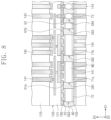
- FIG. 1 is a sectional view schematically illustrating a semiconductor package according to an embodiment of the disclosure.
- FIG. 2 is an enlarged sectional view illustrating a connection region and its neighboring region in a semiconductor package according to an embodiment of the disclosure.
- FIG. 3 is an enlarged sectional view illustrating a portion ‘A’ of FIG. 2 .
- FIG. 4 is a plan view exemplarily illustrating an arrangement of a metal layer and connection terminals of FIG. 2 .
- FIG. 5 is a plan view schematically illustrating a region provided with connection terminals.
- FIG. 6 is an enlarged sectional view illustrating a connection region and its neighboring region in a semiconductor package according to an embodiment of the disclosure.
- FIG. 7 is an enlarged sectional view illustrating a connection region and its neighboring region in a semiconductor package according to an embodiment of the disclosure.
- FIG. 8 is an enlarged sectional view illustrating a connection region and its neighboring region in a semiconductor package according to an embodiment of the disclosure.
- FIG. 9 is an enlarged sectional view illustrating a connection region and its neighboring region in a semiconductor package according to an embodiment of the disclosure.
- FIG. 10 is a plan view illustrating a semiconductor package according to an embodiment of the disclosure.
- FIG. 11 is a sectional view taken along a line I-I′ of FIG. 10 .
- FIG. 1 is a sectional view schematically illustrating a semiconductor package 1 according to an embodiment of the disclosure.
- a package 1 may be provided and may be referred to as a semiconductor chip stack ST.
- the semiconductor chip stack ST may include a plurality of first semiconductor chips 100 and 100 t , a second semiconductor chip 200 , a molding member MD, and an adhesive layer AD, which is provided between the first semiconductor chips 100 and 100 t and between the first semiconductor chip 100 and the second semiconductor chip 200 .
- the first semiconductor chips 100 and 100 t may be stacked on a top surface of the second semiconductor chip 200 in a vertical direction.
- at least one of the first semiconductor chips 100 and 100 t may be a memory chip.
- the memory chip may be one of dynamic random access memory (DRAM) and static random access memory (SRAM) chips.
- the second semiconductor chip 200 may be called a base chip or a buffer chip.
- the second semiconductor chip 200 may be a logic chip.
- the logic chip may be one of graphics processing unit (GPU) and system on chip (SOC) chips.
- the molding member MD may cover side surfaces of the first semiconductor chips 100 and 100 t , the top surface of the second semiconductor chip 200 , and side surfaces of the adhesive layers AD.
- the molding member MD may be formed of or include an epoxy compound.
- Each of the first semiconductor chips 100 may include a first semiconductor substrate 110 , an interconnection layer 120 , a first protection layer 190 (e.g., see FIG. 2 ), a second protection layer 150 , and first penetration electrodes 140 .
- the first semiconductor substrate 110 may be formed of or include silicon.
- the first semiconductor substrate 110 may include a first surface 110 a and a second surface 110 b , which are opposite to each other.
- the interconnection layer 120 may be provided on the first surface 110 a .
- the first protection layer 190 may be provided on a bottom surface of the interconnection layer 120 .
- the first protection layer 190 may be formed of or include an insulating material (e.g., a silicon nitride layer).
- First lower pad groups 160 may be provided on the first protection layer 190 .
- the first lower pad groups 160 may be formed of or include a conductive material (e.g., copper).
- the first lower pad groups 160 may include a first lower voltage pad group 161 , a first lower dummy pad group 162 , and a first lower signal pad group 163 .
- the first lower dummy pad group 162 may be referred to as a lower heat transfer pad group 162 .
- the second protection layer 150 may be provided on the second surface 110 b .
- First upper pad groups 170 may be provided on the second protection layer 150 .
- the first upper pad groups 170 may be formed of or include a conductive material (e.g., copper).
- the first upper pad groups 170 may include a first upper voltage pad group 171 , a first upper dummy pad group 172 , and a first upper signal pad group 173 .
- the first upper dummy pad group 172 may be referred to as an upper heat transfer pad group 172 .
- the first penetration electrodes 140 may be provided to penetrate the first semiconductor substrate 110 .
- the first penetration electrodes 140 may electrically connect the first lower voltage pad group 161 and the first lower signal pad group 163 to the first upper voltage pad group 171 and the first upper signal pad group 173 , respectively.
- Connection terminals CN may be provided on the first lower pad group 160 .
- the connection terminals CN may be provided between the first lower pad group 160 of an upper one of the first semiconductor chips 100 and the first upper pad group 170 of a lower one of the first semiconductor chips 100 .
- connection terminals CN may be formed of or include at least one of conductive materials (e.g., soldering materials).
- conductive materials e.g., soldering materials
- the first semiconductor substrate 110 of the first semiconductor chip 100 t which is the uppermost one of the first semiconductor chips 100 and 100 t , may be thicker than those of the other first semiconductor chips 100 .
- the first semiconductor chip 100 t may not include the first upper pad group 170 and the first penetration electrodes 140 . In an embodiment, the first semiconductor chip 100 t may include the first penetration electrodes 140 but not the first upper pad group 170 .
- the second semiconductor chip 200 may include a second semiconductor substrate 210 , a second interconnection layer 220 , second penetration electrodes 240 , a third protection layer (not shown), a fourth protection layer 250 , second upper pad groups 270 , and lower pads 260 .
- the second upper pad groups 270 may include a second upper voltage pad group 271 , a second upper dummy pad group 272 , and a second upper signal pad group 273 .
- the lower pads 260 may include signal pads and voltage pads.
- Package connection terminals 280 may be provided on the lower pads 260 , respectively.
- the adhesive layer AD may be provided to enclose the connection terminals CN and to prevent an unintended current flow from being produced between the connection terminals CN.
- the adhesive layer AD may be a non-conductive film.
- connection region CR Each of regions between adjacent ones of the first semiconductor chips 100 and between the first and second semiconductor chips 100 and 200 adjacent to each other may be referred to as a connection region CR.
- the first lower pad groups 160 of an upper one of the adjacent first semiconductor chips 100 , the first upper pad groups 170 of a lower one of the adjacent first semiconductor chips 100 , and the connection terminals CN may be placed in the connection region CR between adjacent ones of the first semiconductor chips 100 .
- the connection region CR will be described in more detail below.
- FIG. 2 is an enlarged sectional view illustrating the connection region CR of FIG. 1 and its neighboring region.
- FIG. 3 is an enlarged sectional view illustrating a portion ‘A’ of FIG. 2 .
- FIG. 4 is a plan view exemplarily illustrating an arrangement of a metal layer and connection terminals.
- the first lower voltage pad groups 161 may include a first lower power pad group 161 a and a first lower ground pad group 161 b .
- the first lower power pad group 161 a may include a plurality of first lower power pads 61 a , which are disposed adjacent to each other.
- the first lower ground pad group 161 b may include a plurality of first lower ground pads 61 b , which are disposed adjacent to each other.
- the first lower dummy pad groups 162 may include a plurality of first lower dummy pads 62 , which are disposed adjacent to each other.
- the first lower signal pad group 163 may include a plurality of first lower signal pads 63 , which are disposed adjacent to each other.
- the first upper voltage pad groups 171 may include a first upper power pad group 171 a and a first upper ground pad group 171 b .
- the first upper power pad group 171 a may include a plurality of first upper power pads 71 a , which are disposed adjacent to each other.
- the first upper ground pad group 171 b may include a plurality of first upper ground pads 71 b , which are disposed adjacent to each other.
- the first upper dummy pad groups 172 may include a plurality of first upper dummy pads 72 , which are disposed adjacent to each other.
- the first upper signal pad group 173 may include a plurality of first upper signal pads 73 , which are disposed adjacent to each other.
- the first penetration electrodes 140 may include a power penetration electrode 141 , a ground penetration electrode 142 , and a signal penetration electrode 143 .
- the power penetration electrode 141 may be connected to the first upper power pad 71 a and may be connected to the first lower power pad 61 a through the interconnection layer 120 .
- the ground penetration electrode 142 may be connected to the first upper ground pad 71 b and may be connected to the first lower ground pad 61 b through the interconnection layer 120 .
- the signal penetration electrode 143 may be connected to the first upper signal pad 73 and may be connected to the first lower signal pad 63 through the interconnection layer 120 .
- the interconnection layer 120 may include an insulating layer 121 and metal layers M 1 , M 2 , and M 3 .
- the metal layers M 1 , M 2 , and M 3 may be provided in the insulating layer 121 .
- the insulating layer 121 may be composed of a plurality of insulating layers.
- the insulating layer 121 may include a silicon oxide layer.
- the metal layers M 1 , M 2 , and M 3 may be extended in a first direction D 1 or a second direction D 2 , which is parallel to the first surface 110 a of the first semiconductor substrate 110 .
- the metal layers M 1 , M 2 , and M 3 may include a first metal layer M 1 , a second metal layer M 2 , and a third metal layer M 3 , which are sequentially stacked on the first surface 110 a .
- the metal layers are illustrated to include three metal layers (e.g., M 1 , M 2 , and M 3 ), the disclosure is not limited to the number of the metal layers illustrated.
- the first metal layer M 1 may be in contact with the first penetration electrodes 140 .
- the third metal layer M 3 may correspond to a metal layer that is most adjacent to the first lower power pad group 161 a , the first lower ground pad group 161 b , and the first lower signal pad group 163 . Adjacent ones of the first to third metal layers M 1 to M 3 may be connected to each other through vias interposed therebetween.
- the third metal layer M 3 may have a thickness that is larger than a thickness of the first metal layer M 1 and a thickness of the second metal layer M 2 .
- a thickness T 1 of the third metal layer M 3 may range from 2 ⁇ m to 3 ⁇ m.
- the first metal layer M 1 and the second metal layer M 2 may be formed of or include copper.
- the third metal layer M 3 may be formed of or include, for example, aluminum.
- the third metal layer M 3 may include power lines M 3 a , ground lines M 3 b , and signal lines M 3 c.
- the power lines M 3 a and the ground lines M 3 b may have a first width W 1 in the first direction D 1
- the signal lines M 3 c may have a second width W 2 in the first direction D 1
- the first width W 1 may range from 80 ⁇ m to 120 ⁇ m
- the second width W 2 may range from 8 ⁇ m to 12 ⁇ m.
- the first width W 1 may be larger than five times the second width W 2 .
- Each of the power lines M 3 a and each of the ground lines M 3 b may be extended in the second direction D 2 , which is parallel to the first surface 110 a of the first semiconductor substrate 110 and is not parallel to the first direction D 1 .
- the first lower power pad group 161 a may be in contact with the power line M 3 a . That is, the first lower power pads 61 a may be in contact with the power line M 3 a in a many-to-one manner.
- the first lower ground pad group 161 b may be in contact with the ground line M 3 b .
- the first lower ground pads 61 b may be in contact with the ground line M 3 b in a many-to-one manner.
- Each of the first lower signal pads 63 may be in contact with a corresponding one of the signal lines M 3 c in a one-to-one manner.
- the first lower dummy pad group 162 may be spaced apart from the third metal layer M 3 . Fir, the first lower dummy pads 62 may not be in contact with the third metal layer M 3 .
- the connection terminals CN may include a first connection terminal CN 1 , a second connection terminal CN 2 , a third connection terminal CN 3 , and a fourth connection terminal CN 4 .
- the first connection terminal CN 1 may be provided between the first lower power pad group 161 a of an upper one of the first semiconductor chips 100 and the first upper power pad group 171 a of a lower one of the first semiconductor chips 100 .
- the second connection terminal CN 2 may be provided between the first lower ground pad group 161 b of the upper one of the first semiconductor chips 100 and the first upper ground pad group 171 b of the lower one of the first semiconductor chips 100 .
- the third connection terminal CN 3 may be provided between the first lower dummy pad group 162 of the upper one of the first semiconductor chips 100 and the first upper dummy pad group 172 of the lower one of the first semiconductor chips 100 .
- the fourth connection terminal CN 4 may be provided between each of the first lower signal pads 63 and each of the first upper signal pads 73 .
- the first connection terminal CN 1 may be connected to the first lower power pads 61 a of the upper one of the first semiconductor chips 100 in a one-to-many manner.
- the first connection terminal CN 1 may be connected to the first upper power pads 71 a of the lower one of the first semiconductor chips 100 in a one-to-many manner.
- the second connection terminal CN 2 may be connected to the first lower ground pads 61 b of the upper one of the first semiconductor chips 100 in a one-to-many manner. Furthermore, the second connection terminal CN 2 may be connected to the first upper ground pads 71 b of the lower one of the first semiconductor chips 100 in a one-to-many manner.
- the third connection terminal CN 3 may be connected to the first lower dummy pads 62 of the upper one of the first semiconductor chips 100 in a one-to-many manner. Furthermore, the third connection terminal CN 3 may be connected to the first upper dummy pads 72 of the lower one of the first semiconductor chips 100 in a one-to-many manner.
- each of the first lower dummy pads 62 may be in contact with the third connection terminal CN 3 and the remaining portion may be in contact with the insulating layer 121 and the first protection layer 190 .
- the fourth connection terminal CN 4 may be connected to each of the first lower signal pads 63 of the upper one of the first semiconductor chips 100 in a one-to-one manner. Furthermore, the fourth connection terminal CN 4 may be connected to the upper signal pads 73 of the lower one of the first semiconductor chips 100 in a one-to-one manner.
- Each of the first to third connection terminals CN 1 to CN 3 may have a structure that is composed of merged bumps.
- the power line M 3 a and the ground line M 3 b may be extended in the second direction D 2 and may be spaced apart from each other by a first separation distance P 1 in the first direction D 1 .
- the power line M 3 a and the ground line M 3 b may be alternately arranged.
- the first separation distance P 1 may be about 20 ⁇ m.
- the first separation distance P 1 may be smaller than the first width W 1 .
- the signal lines M 3 c may be extended in the second direction D 2 and may be spaced apart from each other by a second separation distance P 2 in the first direction D 1 .
- the second separation distance P 2 may be about 20 ⁇ m.
- the second separation distance P 2 may be larger than the second width W 2 .
- the first connection terminal CN 1 may be vertically overlapped with the power line M 3 a .
- the second connection terminal CN 2 may be vertically overlapped with the ground line M 3 b .
- the fourth connection terminal CN 4 may be vertically overlapped with the signal line M 3 c.
- the third connection terminal CN 3 may be disposed to be vertically overlapped with a region, on which the power line M 3 a , the ground line M 3 b , and the signal line M 3 c are not disposed.
- the third connection terminal CN 3 may be disposed between the power line M 3 a and the ground line M 3 b or may be disposed to be vertically overlapped with a region between the power or ground line M 3 a or M 3 b and the signal line M 3 c.
- the first and second connection terminals CN 1 and CN 2 may have a width L 1 in the first direction DE
- the width L 1 in the first direction D 1 may be the smallest width.
- a width L 2 in the first direction D 1 may be the smallest width.
- the smallest widths of the first to third connection terminals CN 1 to CN 3 may be larger than the largest width of the fourth connection terminal CN 4 .
- the widths L 1 and L 2 of the first to third connection terminals CN 1 to CN 3 may be larger than a width L 3 of the fourth connection terminal CN 4 .
- An aspect ratio of each of the first to third connection terminals CN 1 to CN 3 may be smaller than an aspect ratio of the fourth connection terminal CN 4 .
- the aspect ratio may mean a value obtained by dividing a thickness or height (i.e., a length in a third direction D 3 ) of an object by a width of the object in the first or second direction D 1 or D 2 .
- the smallest width L 1 or L 2 of the first to third connection terminals CN 1 to CN 3 may be substantially equal to the largest diameter of a first bump BP 1 .
- the fourth connection terminal CN 4 may be a second bump BP 2 .
- a diameter L 4 of the first bump BP 1 may be larger than the largest diameter of the second bump BP 2 .
- a separation distance K 2 between the first lower power pads 61 a may be smaller than a diameter of each of the first lower power pads 61 a .
- the first upper power pad group 171 a , the first lower ground pad group 161 b , the first upper ground pad group 171 b , the first lower dummy pad group 162 , and the first upper dummy pad group 172 may also be configured to have the same distance-diameter relationship as that in the first lower power pad group 161 a ; that is, in each group, a separation distance between pads may be smaller than a diameter of each pad.
- adjacent ones of the first bumps BP 1 may be in contact with each other and may be easily combined with each other, when the first bumps BP 1 are reflowed on the first lower power pads 61 a , the first lower ground pads 61 b , and the first lower dummy pads 62 or when the first semiconductor chips 100 are attached to each other.
- the first lower power pad group 161 a may be spaced apart from the first lower ground pad group 161 b adjacent thereto by a separation distance K 3 , and here, the separation distance K 3 may be equal to or larger than a diameter K 1 of the first lower power pad 61 a .
- the first and second connection terminals CN 1 and CN 2 may not be in contact with each other.
- a diameter K 4 of the first lower signal pad 63 may be smaller than the diameter K 1 of the first lower power pad 61 a .
- the diameter K 4 of the first lower signal pad 63 may be smaller than a diameter of the first lower ground pad 61 b and a diameter of the first lower dummy pad 62 .
- the diameter K 4 of the first lower signal pad 63 may be smaller than or equal to a distance to another first lower signal pad 63 adjacent thereto.
- a first lower power pad group and a first lower ground pad group may be connected to a power line and a ground line, respectively, which have a large area and a large thickness.
- First lower power pads in the first lower power pad groups may be coupled to a first connection terminal in a many-to-one manner, and first lower ground pads in first lower ground pad groups may be coupled to a second connection terminal in a many-to-one manner.
- a first lower dummy pad group may be disposed on a region, in which the power line and the ground line are not disposed, and first lower dummy pads may be coupled to a third connection terminal in a many-to-one manner.
- first and second connection terminals are provided to have an increased area, a heat transfer process from a lower one of the first semiconductor chips toward an upper one of the first semiconductor chips may be effectively performed.
- the third connection terminal is disposed on an unused area, the heat transfer process may be more effectively performed. As a result, it may be possible to improve efficiency of an upward heat transfer process in a semiconductor chip stack or to reduce a thermal resistance of the semiconductor package in a vertical direction.
- FIG. 5 is a plan view schematically illustrating an arrangement of the connection terminals.
- a first connection terminal region CN 1 R or a second connection terminal region CN 2 R may be disposed on a bottom surface of the first semiconductor chip 100 .
- a fourth connection terminal region CN 4 R may be disposed on a center portion of the first semiconductor chip.
- a region, on which the first or second connection terminal region CN 1 R or CN 2 R and the fourth connection terminal region CN 4 R are not disposed, may serve as a third connection terminal region CN 3 R, on which the third connection terminal CN 3 is disposed.
- the third connection terminal region CN 3 R may account for 20% to 50% of a planar area.
- FIG. 6 is an enlarged sectional view illustrating a connection region and its neighboring region according to an embodiment of the disclosure. Except for features to be described below, the package according to the present embodiment may have substantially the same features as those described with reference to FIGS. 1 to 5 , and thus, an overlapping description thereof may be omitted.
- a separation distance K 2 between first lower voltage pads 61 , which are adjacent to each other in the first lower power pad group 161 a , may be equal to or larger than a diameter K 1 of each of the first lower voltage pads 61 .
- a separation distance K 3 between the first lower power and ground pad groups 161 a and 1661b may be larger than the separation distance K 2 between adjacent ones of the first lower voltage pads 61 .
- a diameter of each first bump BP 1 constituting the first connection terminal CN 1 may be larger than 1.5 times a diameter of the first lower voltage pad 61 .
- FIG. 7 is an enlarged sectional view illustrating a connection region and its neighboring region according to an embodiment of the disclosure. Except for features to be described below, the package according to the present embodiment may have substantially the same features as those described with reference to FIGS. 1 to 5 , and thus, an overlapping description thereof may be omitted.
- each of the first to third connection terminals CN 1 to CN 3 may include a metal structure MS.
- the metal structure MS may be formed of or include copper.
- the metal structure MS may have a rectangular shape, when viewed in a sectional view. Some of the metal structures MS may be vertically overlapped with the power line M 3 a and the ground line M 3 b .
- the fourth connection terminal CN 4 may include a bump.
- FIG. 8 is an enlarged sectional view illustrating a connection region and its neighboring region according to an embodiment of the disclosure. Except for features to be described below, the package according to the present embodiment may have substantially the same features as those described with reference to FIGS. 1 to 5 , and thus, an overlapping description thereof may be omitted.
- each of the first lower power pad 61 a , the first lower ground pad 61 b , and the first lower dummy pad 62 may be provided to include a plurality of vias.
- the first upper power pad 71 a may be provided to be in contact with a plurality of power penetration electrodes 141 in a one-to-many manner
- the first upper ground pad 71 b may be provided to be in contact with a plurality of ground penetration electrodes 142 in a one-to-many manner.
- the first upper dummy pad 72 may have a size corresponding to the first lower dummy pad 62 .
- the metal structure MS may be provided between each corresponding pair of the first lower power pad 61 a , the first lower ground pad 61 b , and the first lower dummy pad 62 of the upper one of the first semiconductor chips 100 and the first upper power pad 71 a , the first upper ground pad 71 b , and the first upper dummy pad 72 of the lower one of the first semiconductor chips 100 .
- FIG. 9 is an enlarged sectional view illustrating a connection region and its neighboring region according to an embodiment of the disclosure. Except for features to be described below, the package according to the present embodiment may have substantially the same features as those described with reference to FIGS. 1 to 5 , and thus, an overlapping description thereof may be omitted.
- the first lower power pad 61 a of the upper one of the first semiconductor chips 100 may be in contact with the first upper power pad 71 a of the lower one of the first semiconductor chips 100 .
- the first lower ground pad 61 b of the upper one of the first semiconductor chips 100 may be in contact with the first upper ground pad 71 b of the lower one of the first semiconductor chips 100 .
- the first lower dummy pad 62 of the upper one of the first semiconductor chips 100 may be in contact with the first upper dummy pad 72 of the lower one of the first semiconductor chips 100 .
- the first lower signal pad 63 of the upper one of the first semiconductor chips 100 may be in contact with the first upper signal pad 73 of the lower one of the first semiconductor chips 100 .
- FIG. 10 is a plan view illustrating a semiconductor package 5 according to an embodiment of the disclosure.
- FIG. 11 is a sectional view taken along a line I-I′ of FIG. 10 .
- the semiconductor package 5 may include a package substrate 4 , an interposer 3 , a semiconductor chip stack 1 , and a third semiconductor chip 2 .
- a plurality of the semiconductor chip stacks 1 may be provided.
- two semiconductor chip stacks 1 may be provided on each of two opposite sides of the third semiconductor chip 2 ; that is, four semiconductor chip stacks 1 may be provided in total around the third semiconductor chip 2 .
- the package substrate 4 may be a printed circuit board.
- the interposer 3 may be a silicon interposer or a redistribution interposer.
- the third semiconductor chip 2 may be a logic chip.
- the third semiconductor chip 2 may include a third substrate 310 .
- the third substrate 310 may have a surface, which faces the interposer 3 and serves as an active surface provided with a circuit layer.
- Lower pads 370 may be provided on the active surface.
- Connection terminals 380 may be provided on the lower pads 370 .
- the interposer 3 may include a first pad 430 and a second pad 440 .
- the package connection terminal 280 may be connected to the first pad 430 .
- the connection terminals 380 may be connected to the second pads 440 .
- the third semiconductor chip 2 and the semiconductor chip stack 1 may be electrically connected to each other through the interposer 3 .
- the interposer 3 may include a third pad 420 and may be connected to the package substrate 4 through the third pad 420 and a connection element (e.g., a bonding wire or TSV).
- the package substrate 4 may include an upper pad 520 and a lower pad 530 .
- An outer connection terminal 580 may be provided on the lower pad 530 .
- the package substrate 4 may be electrically connected to an external board (e.g., a motherboard) through the outer connection terminal 580 .
- a first connection terminal, a second connection terminal, and a third connection terminal which are connected to voltage pads, ground pads, and dummy pads, respectively, in a one-to-many manner, may be provided between stacked semiconductor chips.
- the first and second connection terminals may be connected to a thick metal layer of a semiconductor chip placed thereon.
- the first and second connection terminals may be used to effectively exhaust heat, which is generated from an underlying semiconductor chip, in an upward direction.
- the heat dissipation process may be more effectively performed. As a result, it may be possible to reduce a thermal resistance of a semiconductor package in a vertical direction.
- circuits may, for example, be embodied in one or more semiconductor chips, or on substrate supports such as printed circuit boards and the like.
- the circuits constituting a block may be implemented by dedicated hardware, or by a processor (e.g., one or more programmed microprocessors and associated circuitry), or by a combination of dedicated hardware to perform some functions of the block and a processor to perform other functions of the block.
- a processor e.g., one or more programmed microprocessors and associated circuitry
- Each block of the embodiments may be physically separated into two or more interacting and discrete blocks without departing from the scope of the disclosure.
- the blocks of the embodiments may be physically combined into more complex blocks without departing from the scope of the disclosure.
- An aspect of an embodiment may be achieved through instructions stored within a non-transitory storage medium and executed by a processor.
Landscapes
- Engineering & Computer Science (AREA)
- Microelectronics & Electronic Packaging (AREA)
- Power Engineering (AREA)
- Computer Hardware Design (AREA)
- Physics & Mathematics (AREA)
- Condensed Matter Physics & Semiconductors (AREA)
- General Physics & Mathematics (AREA)
- Semiconductor Integrated Circuits (AREA)
- Wire Bonding (AREA)
Abstract
Description
Claims (20)
Applications Claiming Priority (2)
| Application Number | Priority Date | Filing Date | Title |
|---|---|---|---|
| KR10-2021-0127487 | 2021-09-27 | ||
| KR1020210127487A KR20230044858A (en) | 2021-09-27 | 2021-09-27 | Semiconductor package |
Publications (2)
| Publication Number | Publication Date |
|---|---|
| US20230096170A1 US20230096170A1 (en) | 2023-03-30 |
| US12142544B2 true US12142544B2 (en) | 2024-11-12 |
Family
ID=85718880
Family Applications (1)
| Application Number | Title | Priority Date | Filing Date |
|---|---|---|---|
| US17/734,700 Active 2043-05-13 US12142544B2 (en) | 2021-09-27 | 2022-05-02 | Semiconductor package |
Country Status (3)
| Country | Link |
|---|---|
| US (1) | US12142544B2 (en) |
| KR (1) | KR20230044858A (en) |
| CN (1) | CN115881692A (en) |
Families Citing this family (2)
| Publication number | Priority date | Publication date | Assignee | Title |
|---|---|---|---|---|
| KR20230044858A (en) * | 2021-09-27 | 2023-04-04 | 삼성전자주식회사 | Semiconductor package |
| KR20250094137A (en) * | 2023-12-18 | 2025-06-25 | 엘지이노텍 주식회사 | Circuit board and semiconductor package comprising the same |
Citations (44)
| Publication number | Priority date | Publication date | Assignee | Title |
|---|---|---|---|---|
| US20070222050A1 (en) * | 2006-03-17 | 2007-09-27 | Seung Hyun Lee | Stack package utilizing through vias and re-distribution lines |
| US7365418B2 (en) | 2006-08-08 | 2008-04-29 | Via Technologies, Inc. | Multi-chip structure |
| US7863098B2 (en) | 2005-02-23 | 2011-01-04 | Texas Instruments Incorporated | Flip chip package with advanced electrical and thermal properties for high current designs |
| US20110042797A1 (en) * | 2009-08-19 | 2011-02-24 | Samsung Electronics Co., Ltd | Semiconductor package and method of manufacturing the same |
| US20110147945A1 (en) * | 2009-12-17 | 2011-06-23 | Elpida Memory, Inc. | Semiconductor device capable of suppressing generation of cracks in semiconductor chip during manufacturing process |
| US8048794B2 (en) | 2009-08-18 | 2011-11-01 | International Business Machines Corporation | 3D silicon-silicon die stack structure and method for fine pitch interconnection and vertical heat transport |
| US20120319757A1 (en) * | 2011-06-14 | 2012-12-20 | Elpida Memory, Inc. | Semiconductor device having penetration electrodes penetrating through semiconductor chip |
| US9136143B2 (en) | 2011-09-02 | 2015-09-15 | Taiwan Semiconductor Manufacturing Company, Ltd. | Thermally enhanced structure for multi-chip device |
| US20150340340A1 (en) * | 2013-02-05 | 2015-11-26 | Socionext Inc. | Semiconductor device |
| US9269646B2 (en) | 2011-11-14 | 2016-02-23 | Micron Technology, Inc. | Semiconductor die assemblies with enhanced thermal management and semiconductor devices including same |
| US9620433B2 (en) | 2011-08-01 | 2017-04-11 | Tessera, Inc. | Packaged microelectronic elements having blind vias for heat dissipation |
| US9847322B2 (en) | 2016-05-18 | 2017-12-19 | SK Hynix Inc. | Semiconductor packages including through mold ball connectors and methods of manufacturing the same |
| US9875992B2 (en) | 2014-09-11 | 2018-01-23 | Samsung Electronics Co., Ltd. | Semiconductor package having stacked chips and a heat dissipation part and method of fabricating the same |
| US10153261B2 (en) | 2017-04-03 | 2018-12-11 | Cisco Technology, Inc. | Cooling system for high power application specific integrated circuit with embedded high bandwidth memory |
| US20190051634A1 (en) * | 2017-08-09 | 2019-02-14 | Chul Park | Semiconductor packages |
| US20190318990A1 (en) * | 2018-04-16 | 2019-10-17 | Renesas Electronics Corporation | Semiconductor device |
| US20200051884A1 (en) | 2018-08-09 | 2020-02-13 | Intel Corporation | Structures to facilitate heat transfer within package layers to thermal heat sink and motherboard |
| US10573579B2 (en) | 2017-03-08 | 2020-02-25 | Mediatek Inc. | Semiconductor package with improved heat dissipation |
| US20200098719A1 (en) * | 2018-09-21 | 2020-03-26 | Samsung Electronics Co., Ltd. | Semiconductor package and method of manufacturing the same |
| US10811389B2 (en) | 2014-07-01 | 2020-10-20 | Taiwan Semiconductor Manufacturing Company | Semiconductor package for thermal dissipation |
| US10872835B1 (en) | 2019-07-03 | 2020-12-22 | Micron Technology, Inc. | Semiconductor assemblies including vertically integrated circuits and methods of manufacturing the same |
| US20210249382A1 (en) * | 2020-02-11 | 2021-08-12 | Samsung Electronics Co., Ltd. | Semiconductor package and method of manufacturing semiconductor package |
| US20230096170A1 (en) * | 2021-09-27 | 2023-03-30 | Samsung Electronics Co., Ltd. | Semiconductor package |
| US20230132272A1 (en) * | 2021-10-22 | 2023-04-27 | Samsung Electronics Co., Ltd. | Semiconductor device and semiconductor package including the same |
| US20230139657A1 (en) * | 2021-11-03 | 2023-05-04 | Samsung Electronics Co., Ltd. | Semiconductor package |
| US20230133322A1 (en) * | 2021-11-02 | 2023-05-04 | Samsung Electronics Co., Ltd. | Semiconductor package and method of manufacturing the same |
| US20230154894A1 (en) * | 2021-11-18 | 2023-05-18 | Samsung Electronics Co., Ltd. | Three-dimensional integrated circuit structure and a method of fabricating the same |
| US20230178533A1 (en) * | 2021-12-02 | 2023-06-08 | Samsung Electronics Co., Ltd. | Semiconductor device |
| US20230187380A1 (en) * | 2021-12-10 | 2023-06-15 | Samsung Electronics Co., Ltd. | Semiconductor package including a barrier structure |
| US20230207414A1 (en) * | 2021-12-28 | 2023-06-29 | Samsung Electronics Co., Ltd. | Semiconductor package having improved heat dissipation characteristics |
| WO2023239188A1 (en) * | 2022-06-08 | 2023-12-14 | 엘지이노텍 주식회사 | Semiconductor package |
| US20230420403A1 (en) * | 2022-06-28 | 2023-12-28 | Samsung Electronics Co., Ltd. | Semiconductor package including a plurality of semiconductor chips |
| US20240006272A1 (en) * | 2022-07-04 | 2024-01-04 | Samsung Electronics Co., Ltd. | Semiconductor package and method of manufacturing the same |
| US20240030103A1 (en) * | 2022-07-19 | 2024-01-25 | Samsung Electronics Co., Ltd. | Semiconductor package |
| US20240063167A1 (en) * | 2022-08-18 | 2024-02-22 | Samsung Electronics Co., Ltd. | Semiconductor package manufactured through a thermocompression process using a non-conductive film (ncf) |
| US20240145416A1 (en) * | 2022-10-28 | 2024-05-02 | Samsung Electronics Co., Ltd. | Substrate bonding method |
| US20240162195A1 (en) * | 2022-11-16 | 2024-05-16 | Samsung Electronics Co., Ltd. | Semiconductor package and method of manufacturing the same |
| US20240170440A1 (en) * | 2022-11-18 | 2024-05-23 | Samsung Electronics Co., Ltd. | Semiconductor package |
| US20240186277A1 (en) * | 2022-12-01 | 2024-06-06 | Samsung Electronics Co., Ltd. | Semiconductor package |
| US20240186294A1 (en) * | 2021-01-11 | 2024-06-06 | Samsung Electronics Co., Ltd. | Semiconductor package including plurality of semiconductor chips and method for manufacturing the same |
| US20240186290A1 (en) * | 2022-12-02 | 2024-06-06 | Samsung Electronics Co., Ltd. | Semiconductor package |
| US20240194624A1 (en) * | 2022-12-13 | 2024-06-13 | Samsung Electronics Co., Ltd. | Semiconductor chip and semiconductor package including the same |
| US20240196618A1 (en) * | 2022-12-07 | 2024-06-13 | Samsung Electronics Co., Ltd. | Integrated circuit device and electronic system including the same |
| US20240203960A1 (en) * | 2022-12-19 | 2024-06-20 | Samsung Electronics Co., Ltd. | Semiconductor package |
-
2021
- 2021-09-27 KR KR1020210127487A patent/KR20230044858A/en active Pending
-
2022
- 2022-05-02 US US17/734,700 patent/US12142544B2/en active Active
- 2022-09-19 CN CN202211140509.7A patent/CN115881692A/en active Pending
Patent Citations (58)
| Publication number | Priority date | Publication date | Assignee | Title |
|---|---|---|---|---|
| US7863098B2 (en) | 2005-02-23 | 2011-01-04 | Texas Instruments Incorporated | Flip chip package with advanced electrical and thermal properties for high current designs |
| US7598617B2 (en) * | 2006-03-17 | 2009-10-06 | Hynix Semiconductor Inc. | Stack package utilizing through vias and re-distribution lines |
| US20070222050A1 (en) * | 2006-03-17 | 2007-09-27 | Seung Hyun Lee | Stack package utilizing through vias and re-distribution lines |
| US7365418B2 (en) | 2006-08-08 | 2008-04-29 | Via Technologies, Inc. | Multi-chip structure |
| US8048794B2 (en) | 2009-08-18 | 2011-11-01 | International Business Machines Corporation | 3D silicon-silicon die stack structure and method for fine pitch interconnection and vertical heat transport |
| US20130203219A1 (en) * | 2009-08-19 | 2013-08-08 | Ji-Hyun Park | Semiconductor package and method of manufacturing the same |
| US20110042797A1 (en) * | 2009-08-19 | 2011-02-24 | Samsung Electronics Co., Ltd | Semiconductor package and method of manufacturing the same |
| US8709879B2 (en) * | 2009-08-19 | 2014-04-29 | Samsung Electronics Co., Ltd. | Method of forming a semiconductor package |
| US8426959B2 (en) * | 2009-08-19 | 2013-04-23 | Samsung Electronics Co., Ltd. | Semiconductor package and method of manufacturing the same |
| US20110147945A1 (en) * | 2009-12-17 | 2011-06-23 | Elpida Memory, Inc. | Semiconductor device capable of suppressing generation of cracks in semiconductor chip during manufacturing process |
| US8461690B2 (en) * | 2009-12-17 | 2013-06-11 | Elpida Memory, Inc. | Semiconductor device capable of suppressing generation of cracks in semiconductor chip during manufacturing process |
| US20120319757A1 (en) * | 2011-06-14 | 2012-12-20 | Elpida Memory, Inc. | Semiconductor device having penetration electrodes penetrating through semiconductor chip |
| US9620433B2 (en) | 2011-08-01 | 2017-04-11 | Tessera, Inc. | Packaged microelectronic elements having blind vias for heat dissipation |
| US9136143B2 (en) | 2011-09-02 | 2015-09-15 | Taiwan Semiconductor Manufacturing Company, Ltd. | Thermally enhanced structure for multi-chip device |
| US9269646B2 (en) | 2011-11-14 | 2016-02-23 | Micron Technology, Inc. | Semiconductor die assemblies with enhanced thermal management and semiconductor devices including same |
| US20150340340A1 (en) * | 2013-02-05 | 2015-11-26 | Socionext Inc. | Semiconductor device |
| US9318470B2 (en) * | 2013-02-05 | 2016-04-19 | Socionext Inc. | Semiconductor device |
| US10811389B2 (en) | 2014-07-01 | 2020-10-20 | Taiwan Semiconductor Manufacturing Company | Semiconductor package for thermal dissipation |
| US9875992B2 (en) | 2014-09-11 | 2018-01-23 | Samsung Electronics Co., Ltd. | Semiconductor package having stacked chips and a heat dissipation part and method of fabricating the same |
| US9847322B2 (en) | 2016-05-18 | 2017-12-19 | SK Hynix Inc. | Semiconductor packages including through mold ball connectors and methods of manufacturing the same |
| US10573579B2 (en) | 2017-03-08 | 2020-02-25 | Mediatek Inc. | Semiconductor package with improved heat dissipation |
| US10153261B2 (en) | 2017-04-03 | 2018-12-11 | Cisco Technology, Inc. | Cooling system for high power application specific integrated circuit with embedded high bandwidth memory |
| US10741526B2 (en) * | 2017-08-09 | 2020-08-11 | Samsung Electronics Co., Ltd. | Semiconductor packages |
| US20190237432A1 (en) * | 2017-08-09 | 2019-08-01 | Samsung Electronics Co., Ltd. | Semiconductor packages |
| US10319702B2 (en) * | 2017-08-09 | 2019-06-11 | Samsung Electronics Co., Ltd. | Semiconductor packages |
| US20190051634A1 (en) * | 2017-08-09 | 2019-02-14 | Chul Park | Semiconductor packages |
| US20190318990A1 (en) * | 2018-04-16 | 2019-10-17 | Renesas Electronics Corporation | Semiconductor device |
| US20200051884A1 (en) | 2018-08-09 | 2020-02-13 | Intel Corporation | Structures to facilitate heat transfer within package layers to thermal heat sink and motherboard |
| US20200098719A1 (en) * | 2018-09-21 | 2020-03-26 | Samsung Electronics Co., Ltd. | Semiconductor package and method of manufacturing the same |
| US10872835B1 (en) | 2019-07-03 | 2020-12-22 | Micron Technology, Inc. | Semiconductor assemblies including vertically integrated circuits and methods of manufacturing the same |
| US11569200B2 (en) * | 2020-02-11 | 2023-01-31 | Samsung Electronics Co., Ltd. | Semiconductor package and method of manufacturing semiconductor package |
| US20230163099A1 (en) * | 2020-02-11 | 2023-05-25 | Samsung Electronics Co., Ltd. | Semiconductor package |
| US20210249382A1 (en) * | 2020-02-11 | 2021-08-12 | Samsung Electronics Co., Ltd. | Semiconductor package and method of manufacturing semiconductor package |
| US20240186294A1 (en) * | 2021-01-11 | 2024-06-06 | Samsung Electronics Co., Ltd. | Semiconductor package including plurality of semiconductor chips and method for manufacturing the same |
| US20230096170A1 (en) * | 2021-09-27 | 2023-03-30 | Samsung Electronics Co., Ltd. | Semiconductor package |
| CN115881692A (en) * | 2021-09-27 | 2023-03-31 | 三星电子株式会社 | Semiconductor package |
| TW202314988A (en) * | 2021-09-27 | 2023-04-01 | 南韓商三星電子股份有限公司 | Semiconductor package |
| US20230132272A1 (en) * | 2021-10-22 | 2023-04-27 | Samsung Electronics Co., Ltd. | Semiconductor device and semiconductor package including the same |
| US20230133322A1 (en) * | 2021-11-02 | 2023-05-04 | Samsung Electronics Co., Ltd. | Semiconductor package and method of manufacturing the same |
| US20230139657A1 (en) * | 2021-11-03 | 2023-05-04 | Samsung Electronics Co., Ltd. | Semiconductor package |
| CN116137264A (en) * | 2021-11-18 | 2023-05-19 | 三星电子株式会社 | Three-dimensional integrated circuit structure and its manufacturing method |
| US20230154894A1 (en) * | 2021-11-18 | 2023-05-18 | Samsung Electronics Co., Ltd. | Three-dimensional integrated circuit structure and a method of fabricating the same |
| US20230178533A1 (en) * | 2021-12-02 | 2023-06-08 | Samsung Electronics Co., Ltd. | Semiconductor device |
| US20230187380A1 (en) * | 2021-12-10 | 2023-06-15 | Samsung Electronics Co., Ltd. | Semiconductor package including a barrier structure |
| US20230207414A1 (en) * | 2021-12-28 | 2023-06-29 | Samsung Electronics Co., Ltd. | Semiconductor package having improved heat dissipation characteristics |
| WO2023239188A1 (en) * | 2022-06-08 | 2023-12-14 | 엘지이노텍 주식회사 | Semiconductor package |
| US20230420403A1 (en) * | 2022-06-28 | 2023-12-28 | Samsung Electronics Co., Ltd. | Semiconductor package including a plurality of semiconductor chips |
| US20240006272A1 (en) * | 2022-07-04 | 2024-01-04 | Samsung Electronics Co., Ltd. | Semiconductor package and method of manufacturing the same |
| US20240030103A1 (en) * | 2022-07-19 | 2024-01-25 | Samsung Electronics Co., Ltd. | Semiconductor package |
| US20240063167A1 (en) * | 2022-08-18 | 2024-02-22 | Samsung Electronics Co., Ltd. | Semiconductor package manufactured through a thermocompression process using a non-conductive film (ncf) |
| US20240145416A1 (en) * | 2022-10-28 | 2024-05-02 | Samsung Electronics Co., Ltd. | Substrate bonding method |
| US20240162195A1 (en) * | 2022-11-16 | 2024-05-16 | Samsung Electronics Co., Ltd. | Semiconductor package and method of manufacturing the same |
| US20240170440A1 (en) * | 2022-11-18 | 2024-05-23 | Samsung Electronics Co., Ltd. | Semiconductor package |
| US20240186277A1 (en) * | 2022-12-01 | 2024-06-06 | Samsung Electronics Co., Ltd. | Semiconductor package |
| US20240186290A1 (en) * | 2022-12-02 | 2024-06-06 | Samsung Electronics Co., Ltd. | Semiconductor package |
| US20240196618A1 (en) * | 2022-12-07 | 2024-06-13 | Samsung Electronics Co., Ltd. | Integrated circuit device and electronic system including the same |
| US20240194624A1 (en) * | 2022-12-13 | 2024-06-13 | Samsung Electronics Co., Ltd. | Semiconductor chip and semiconductor package including the same |
| US20240203960A1 (en) * | 2022-12-19 | 2024-06-20 | Samsung Electronics Co., Ltd. | Semiconductor package |
Also Published As
| Publication number | Publication date |
|---|---|
| CN115881692A (en) | 2023-03-31 |
| TW202314988A (en) | 2023-04-01 |
| KR20230044858A (en) | 2023-04-04 |
| US20230096170A1 (en) | 2023-03-30 |
Similar Documents
| Publication | Publication Date | Title |
|---|---|---|
| US7598617B2 (en) | Stack package utilizing through vias and re-distribution lines | |
| US10741526B2 (en) | Semiconductor packages | |
| US10784244B2 (en) | Semiconductor package including multiple semiconductor chips and method of manufacturing the semiconductor package | |
| CN108140636B (en) | Semiconductor package, semiconductor stack package, and memory module | |
| US11031371B2 (en) | Semiconductor package and method of fabricating semiconductor package | |
| KR102587976B1 (en) | Semiconductor packages | |
| US12237302B2 (en) | Semiconductor package | |
| KR102517464B1 (en) | Semiconductor package include bridge die spaced apart semiconductor die | |
| US11158621B2 (en) | Double side mounted large MCM package with memory channel length reduction | |
| JP2001257307A (en) | Semiconductor device | |
| KR20090034180A (en) | A semiconductor package including an interposer, an electronic device having the same, and a manufacturing method of the semiconductor package | |
| US20150035142A1 (en) | Multi-chip package | |
| US20240203960A1 (en) | Semiconductor package | |
| US12142544B2 (en) | Semiconductor package | |
| US20250336839A1 (en) | Redistribution substrate and semiconductor package including the same | |
| US20110272692A1 (en) | Size variable type semiconductor chip and semiconductor package using the same | |
| US8283765B2 (en) | Semiconductor chip and stacked semiconductor package having the same | |
| US8304879B2 (en) | Spiral staircase shaped stacked semiconductor package and method for manufacturing the same | |
| US8829665B2 (en) | Semiconductor chip and stack package having the same | |
| KR20140028209A (en) | Semiconductor chip, semiconductor stack package having the chip and chip selection method for the same | |
| US9318470B2 (en) | Semiconductor device | |
| TWI911478B (en) | Semiconductor package | |
| US20250183238A1 (en) | Stack chip package | |
| US20230422521A1 (en) | Stack-type semiconductor package | |
| KR20100050981A (en) | Semiconductor package and stack package using the same |
Legal Events
| Date | Code | Title | Description |
|---|---|---|---|
| FEPP | Fee payment procedure |
Free format text: ENTITY STATUS SET TO UNDISCOUNTED (ORIGINAL EVENT CODE: BIG.); ENTITY STATUS OF PATENT OWNER: LARGE ENTITY |
|
| AS | Assignment |
Owner name: SAMSUNG ELECTRONICS CO., LTD., KOREA, REPUBLIC OF Free format text: ASSIGNMENT OF ASSIGNORS INTEREST;ASSIGNORS:KIM, TAEHWAN;KIM, YOUNG-DEUK;KIM, JAE CHOON;AND OTHERS;REEL/FRAME:059793/0431 Effective date: 20220307 |
|
| STPP | Information on status: patent application and granting procedure in general |
Free format text: DOCKETED NEW CASE - READY FOR EXAMINATION |
|
| STPP | Information on status: patent application and granting procedure in general |
Free format text: NOTICE OF ALLOWANCE MAILED -- APPLICATION RECEIVED IN OFFICE OF PUBLICATIONS |
|
| ZAAB | Notice of allowance mailed |
Free format text: ORIGINAL CODE: MN/=. |
|
| STPP | Information on status: patent application and granting procedure in general |
Free format text: PUBLICATIONS -- ISSUE FEE PAYMENT VERIFIED |
|
| STCF | Information on status: patent grant |
Free format text: PATENTED CASE |