US12136379B2 - Display panel - Google Patents
Display panel Download PDFInfo
- Publication number
- US12136379B2 US12136379B2 US18/349,184 US202318349184A US12136379B2 US 12136379 B2 US12136379 B2 US 12136379B2 US 202318349184 A US202318349184 A US 202318349184A US 12136379 B2 US12136379 B2 US 12136379B2
- Authority
- US
- United States
- Prior art keywords
- wiring
- regions
- region
- driving electrode
- included angle
- Prior art date
- Legal status (The legal status is an assumption and is not a legal conclusion. Google has not performed a legal analysis and makes no representation as to the accuracy of the status listed.)
- Active
Links
Images


Classifications
-
- H—ELECTRICITY
- H10—SEMICONDUCTOR DEVICES; ELECTRIC SOLID-STATE DEVICES NOT OTHERWISE PROVIDED FOR
- H10K—ORGANIC ELECTRIC SOLID-STATE DEVICES
- H10K59/00—Integrated devices, or assemblies of multiple devices, comprising at least one organic light-emitting element covered by group H10K50/00
- H10K59/10—OLED displays
- H10K59/12—Active-matrix OLED [AMOLED] displays
- H10K59/131—Interconnections, e.g. wiring lines or terminals
-
- G—PHYSICS
- G09—EDUCATION; CRYPTOGRAPHY; DISPLAY; ADVERTISING; SEALS
- G09G—ARRANGEMENTS OR CIRCUITS FOR CONTROL OF INDICATING DEVICES USING STATIC MEANS TO PRESENT VARIABLE INFORMATION
- G09G3/00—Control arrangements or circuits, of interest only in connection with visual indicators other than cathode-ray tubes
- G09G3/20—Control arrangements or circuits, of interest only in connection with visual indicators other than cathode-ray tubes for presentation of an assembly of a number of characters, e.g. a page, by composing the assembly by combination of individual elements arranged in a matrix no fixed position being assigned to or needed to be assigned to the individual characters or partial characters
- G09G3/2092—Details of a display terminals using a flat panel, the details relating to the control arrangement of the display terminal and to the interfaces thereto
-
- G—PHYSICS
- G09—EDUCATION; CRYPTOGRAPHY; DISPLAY; ADVERTISING; SEALS
- G09G—ARRANGEMENTS OR CIRCUITS FOR CONTROL OF INDICATING DEVICES USING STATIC MEANS TO PRESENT VARIABLE INFORMATION
- G09G2300/00—Aspects of the constitution of display devices
- G09G2300/04—Structural and physical details of display devices
- G09G2300/0421—Structural details of the set of electrodes
- G09G2300/0426—Layout of electrodes and connections
-
- G—PHYSICS
- G09—EDUCATION; CRYPTOGRAPHY; DISPLAY; ADVERTISING; SEALS
- G09G—ARRANGEMENTS OR CIRCUITS FOR CONTROL OF INDICATING DEVICES USING STATIC MEANS TO PRESENT VARIABLE INFORMATION
- G09G2300/00—Aspects of the constitution of display devices
- G09G2300/04—Structural and physical details of display devices
- G09G2300/0439—Pixel structures
-
- G—PHYSICS
- G09—EDUCATION; CRYPTOGRAPHY; DISPLAY; ADVERTISING; SEALS
- G09G—ARRANGEMENTS OR CIRCUITS FOR CONTROL OF INDICATING DEVICES USING STATIC MEANS TO PRESENT VARIABLE INFORMATION
- G09G2300/00—Aspects of the constitution of display devices
- G09G2300/04—Structural and physical details of display devices
- G09G2300/0469—Details of the physics of pixel operation
-
- G—PHYSICS
- G09—EDUCATION; CRYPTOGRAPHY; DISPLAY; ADVERTISING; SEALS
- G09G—ARRANGEMENTS OR CIRCUITS FOR CONTROL OF INDICATING DEVICES USING STATIC MEANS TO PRESENT VARIABLE INFORMATION
- G09G2310/00—Command of the display device
- G09G2310/02—Addressing, scanning or driving the display screen or processing steps related thereto
- G09G2310/0264—Details of driving circuits
-
- G—PHYSICS
- G09—EDUCATION; CRYPTOGRAPHY; DISPLAY; ADVERTISING; SEALS
- G09G—ARRANGEMENTS OR CIRCUITS FOR CONTROL OF INDICATING DEVICES USING STATIC MEANS TO PRESENT VARIABLE INFORMATION
- G09G3/00—Control arrangements or circuits, of interest only in connection with visual indicators other than cathode-ray tubes
- G09G3/20—Control arrangements or circuits, of interest only in connection with visual indicators other than cathode-ray tubes for presentation of an assembly of a number of characters, e.g. a page, by composing the assembly by combination of individual elements arranged in a matrix no fixed position being assigned to or needed to be assigned to the individual characters or partial characters
- G09G3/22—Control arrangements or circuits, of interest only in connection with visual indicators other than cathode-ray tubes for presentation of an assembly of a number of characters, e.g. a page, by composing the assembly by combination of individual elements arranged in a matrix no fixed position being assigned to or needed to be assigned to the individual characters or partial characters using controlled light sources
- G09G3/30—Control arrangements or circuits, of interest only in connection with visual indicators other than cathode-ray tubes for presentation of an assembly of a number of characters, e.g. a page, by composing the assembly by combination of individual elements arranged in a matrix no fixed position being assigned to or needed to be assigned to the individual characters or partial characters using controlled light sources using electroluminescent panels
- G09G3/32—Control arrangements or circuits, of interest only in connection with visual indicators other than cathode-ray tubes for presentation of an assembly of a number of characters, e.g. a page, by composing the assembly by combination of individual elements arranged in a matrix no fixed position being assigned to or needed to be assigned to the individual characters or partial characters using controlled light sources using electroluminescent panels semiconductive, e.g. using light-emitting diodes [LED]
- G09G3/3208—Control arrangements or circuits, of interest only in connection with visual indicators other than cathode-ray tubes for presentation of an assembly of a number of characters, e.g. a page, by composing the assembly by combination of individual elements arranged in a matrix no fixed position being assigned to or needed to be assigned to the individual characters or partial characters using controlled light sources using electroluminescent panels semiconductive, e.g. using light-emitting diodes [LED] organic, e.g. using organic light-emitting diodes [OLED]
-
- H—ELECTRICITY
- H10—SEMICONDUCTOR DEVICES; ELECTRIC SOLID-STATE DEVICES NOT OTHERWISE PROVIDED FOR
- H10K—ORGANIC ELECTRIC SOLID-STATE DEVICES
- H10K2102/00—Constructional details relating to the organic devices covered by this subclass
- H10K2102/301—Details of OLEDs
- H10K2102/302—Details of OLEDs of OLED structures
- H10K2102/3023—Direction of light emission
- H10K2102/3031—Two-side emission, e.g. transparent OLEDs [TOLED]
Definitions
- the invention relates to a display device, and more particularly, to a display panel.
- the transparent display panel is a display panel having a certain degree of transparency. The user may see the image information displayed on the transparent display panel, and may see the background information behind the transparent display panel. Transparent panels are suitable for a variety of scenarios such as vending machines, car windows, and shop windows.
- the transparent display panel generally adopts liquid-crystal display (LCD), organic light-emitting diode (OLED), or micro light-emitting diode (pLED) techniques.
- the transparent display panel has an element setting region with low average optical transmission and a transmission region with high average optical transmission.
- the element setting region may be used for setting the driving electrodes of LCD or self-luminous diodes (for example, OLED or pLED) and related circuit wiring, and the transmission regions allow the user to receive the background behind the transparent display panel. Since the transmission regions are divided into a plurality of small transmission regions by the circuit wiring, this may lead to the generation of diffraction phenomenon and reduce image quality. Therefore, how to reduce the diffraction phenomenon in the transparent display panel and keep the transparency of the transparent display panel to a certain degree has become an urgent issue requiring immediate attention.
- the invention provides a display panel that may improve first-order diffraction and the diffraction of high-frequency terms at the same time, so as to improve the image quality of the display panel.
- a display panel of the invention includes a plurality of driving electrode regions and a plurality of wiring regions connected between the driving electrode regions.
- a (2n ⁇ 1)th driving electrode region, a (2n)th driving electrode region, a (2n+1)th driving electrode region and a (2n+2)th driving electrode region are arranged in sequence along an arrangement direction, a (2n ⁇ 1)th wiring region extended from the (2n ⁇ 1)th driving electrode region toward the (2n)th driving electrode region has a wiring extending direction forming a first included angle with the arrangement direction, and a (2n)th wiring region extended from the (2n)th driving electrode region toward the (2n+1)th driving electrode region has a wiring extending direction forming a second included angle with the arrangement direction, and a (2n+1)th wiring region extended from the (2n+1)th driving electrode region toward the (2n+2)th driving electrode region has a wiring extending direction forming a third included angle with the arrangement direction, wherein n is a positive integer. At least one of the first included angle, the second included angle and the
- the (2n ⁇ 1)th wiring region and the (2n)th wiring region are respectively located on two opposite sides of straight connecting lines of the (2n ⁇ 1)th driving electrode region, the (2n)th driving electrode region, and the (2n+1)th driving electrode region.
- each of the wiring regions includes a plurality of segments, and two adjacent segments have different extending directions.
- each of the wiring regions is first extended from one of the driving electrode regions along a first direction and then extended along a second direction toward the next driving electrode region, and the first direction is intersected with the second direction.
- angles of the first included angle, the second included angle and the third included angle are respectively 5 degrees to 44 degrees.
- the driving electrode regions and the wiring regions have an average optical transmittance of less than 10%.
- the driving electrode regions and the wiring regions enclose a plurality of transmission regions, and two adjacent transmission regions arranged along the arrangement direction have different geometric shapes.
- an average optical transmittance of the transmission regions is 10% to 99%.
- the display panel further includes a plurality of pixel units, and the pixel units are respectively disposed in the driving electrode regions.
- each of the pixel units includes a plurality of light-emitting units and a pixel circuit element.
- the display panel further includes a display medium, wherein each of the pixel units further includes a plurality of pixel electrodes, wherein the pixel electrodes are electrically connected to the pixel circuit elements, and the display medium is adapted to be driven by the pixel units.
- angles of the first included angle, the second included angle and the third included angle are different from each other.
- two of the first included angle, the second included angle and the third included angle have the same angle.
- the first included angle and the second included angle have the same sign, and a sign of the third included angle is opposite to the first included angle.
- the arrangement direction comprises an x-direction or a y-direction intersecting the x-direction, the plurality of driving electrode regions arranged along the x-direction and the y-direction to form a periodic array, and each of the plurality of wiring regions between the plurality of driving electrode regions has a wiring extending direction forming an included angle with the arrangement direction.
- a portion of the plurality of wiring regions constitutes a plurality of gate line regions and the other portion of the plurality of wiring regions constitutes a plurality of data line regions.
- the plurality of gate line regions are arranged in the y-direction and extends along the x-direction as its main extending direction.
- the plurality of data line regions are arranged in the x-direction and extends along the y-direction as its main extending direction.
- adjacent gate line regions are symmetrical about an axis.
- At least one of the plurality of gate line regions are shifted a driving electrode region pitch relative to its adjacent gate line region.
- the driving electrode region pitch is defined as a distance between centers of two adjacent driving electrode regions.
- signs of the included angles with the x-direction of the wiring extending directions of the wiring regions contained in the same gate line region or the same data line region are repeated periodically in positive and negative configuration, in positive, positive and negative configuration, in negative, negative and positive configuration or in positive, positive, negative and negative configuration.
- Signs of the included angles with the y-direction of the wiring extending directions of the wiring regions contained in the same data line region are repeated periodically in positive and negative configuration, in positive, positive and negative configuration, in negative, negative and positive configuration or in positive, positive, negative and negative configuration.
- the wiring extending direction of the wiring regions contained in the same gate line region or the same data line region are periodically repeated.
- the arrangement direction is defined as an extension direction of the shortest connection line between two adjacent driving electrode regions.
- the included angles of the wiring extending directions of the wiring regions between adjacent driving electrode regions and the arrangement directions thereof are arranged in a positive and negative alternate configuration in the arrangement directions to effectively reduce the diffraction intensity of first-order diffraction and high-frequency terms, thereby improving the image quality of the display panel.
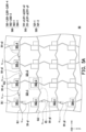
- FIG. 1 A is a schematic top view of a display panel according to an embodiment of the invention.
- FIG. 1 B is a partial enlarged schematic top view of the display panel of FIG. 1 A .
- FIG. 1 C is a partial enlarged schematic top view of the display panel of FIG. 1 A .
- FIG. 2 A is a schematic top view of a display panel according to an embodiment of the invention.
- FIG. 2 B is a partial enlarged schematic top view of the display panel of FIG. 2 A .
- FIG. 3 is a schematic top view of a display panel according to an embodiment of the invention.
- FIG. 4 A is a schematic top view of a display panel according to an embodiment of the invention.
- FIG. 4 B is a partial enlarged schematic top view of the display panel of FIG. 4 A .
- FIG. 5 A is a schematic top view of a display panel according to an embodiment of the invention.
- FIG. 5 B is a partial enlarged schematic top view of the display panel of FIG. 5 A .
- FIG. 6 A is a schematic top view of a display panel according to an embodiment of the invention.
- FIG. 6 B is a partial enlarged schematic top view of the display panel of FIG. 6 A .
- FIG. 7 A is a schematic top view of a display panel according to an embodiment of the invention.
- FIG. 7 B is a partial enlarged schematic top view of the display panel of FIG. 7 A .
- FIG. 8 A is a schematic top view of a display panel according to an embodiment of the invention.
- FIG. 8 B is a partial enlarged schematic top view of the display panel of FIG. 8 A .
- FIG. 9 is a schematic top view of a display panel according to an embodiment of the invention.
- FIG. 10 A is a schematic top view of a display panel according to an embodiment of the invention.
- FIG. 10 B is a partial enlarged schematic top view of the display panel of FIG. 10 A .
- FIG. 11 A is a schematic top view of a display panel according to an embodiment of the invention.
- FIG. 11 B is a partial enlarged schematic top view of the display panel of FIG. 11 A .
- “about”, “approximately”, or “substantially” includes the stated value and the average value within an acceptable deviation of the particular value as determined by one of ordinary skill in the art, taking into account the measurement in question and the specific amount of measurement-related error (i.e., the limitations of the measurement system). For example, “about” may mean within one or a plurality of standard deviations of the stated value, or within ⁇ 30%, ⁇ 20%, ⁇ 10%, ⁇ 5%. Furthermore, as used herein, “about”, “approximately”, or “substantially” may encompass an acceptable range of deviation or standard deviation depending on optical properties, etching properties, or other properties.
- FIG. 1 A is a schematic top view of a display panel according to an embodiment of the invention.
- FIG. 1 B is a partial enlarged schematic top view of a region R 1 of the display panel of FIG. 1 A .
- FIG. 1 C is a partial enlarged schematic top view of a region R 2 of the display panel of FIG. 1 A .
- a display panel 10 includes a plurality of driving electrode regions 100 and a plurality of wiring regions 110 .
- the plurality of driving electrode regions 100 may be sequentially arranged along the arrangement direction to form a periodic array, and the arrangement direction may be, for example, the x-direction or the y-direction intersecting the x-direction.
- the arrangement direction may be defined as an extension direction of the shortest connection line between two adjacent driving electrode regions.
- the shortest connection line between two adjacent driving electrode regions may refer to a connection line between centers of the two adjacent driving electrode regions.
- the x-direction may be perpendicular to the y-direction, but is not limited thereto.
- the plurality of wiring regions 110 are connected between the driving electrode regions 100 .
- the plurality of wiring regions 110 may be divided into a plurality of gate line regions GL and a plurality of data line regions DL, wherein the main extending directions of the gate line regions GL and the data line regions DL are different.
- One or a plurality of wirings may be disposed in each of the plurality of wiring regions 110 , and the wiring material is, for example, metal, but the invention is not limited thereto.
- the wiring regions 110 may be understood as the regions where the wiring is located, and the distribution of the wiring regions 110 may be determined from the outline of the wiring.
- the wiring in the wiring regions 110 may be used to transmit signals to the corresponding driving electrode regions 100 .
- the (2n ⁇ 1)th wiring region 110 extended from the (2n ⁇ 1)th driving electrode region 100 toward the (2n)th driving electrode region 100 has a wiring extending direction forming a positive included angle with the arrangement direction
- the (2n)th wiring region 110 extended from the (2n)th driving electrode region 110 toward the (2n+1)th driving electrode region 100 has a wiring extending direction forming a negative included angle with the arrangement direction, wherein n is a positive integer.
- the (2n ⁇ 1)th wiring region 110 and the (2n)th wiring region 110 are respectively located on two opposite sides of the straight connecting lines of the (2n ⁇ 1)th driving electrode region 100 , the (2n)th driving electrode region 100 , and the (2n+1)th driving electrode region 100 .
- the plurality of driving electrode regions 100 include driving electrode regions 101 - 1 , 101 - 2 , 101 - 3 , and 101 - 4 sequentially arranged in the same column along the x-direction
- the plurality of wiring regions 110 may include wiring regions 111 - x 1 , 111 - x 2 , and 111 - x 3 alternately arranged with the driving electrode regions 101 - 1 , 101 - 2 , 101 - 3 , and 101 - 4 along the x-direction.
- the wiring region 111 - x 1 is located between the driving electrode regions 101 - 1 and 101 - 2
- the wiring region 111 - x 2 is located between the driving electrode regions 101 - 2 and 101 - 3
- the wiring region 111 - x 3 is located between the driving electrode regions 101 - 3 and 101 - 4 .
- the wiring region 111 - x 1 and the wiring region 111 - x 2 are located on two opposite sides of the straight connecting lines of the driving electrode regions 101 - 1 , 101 - 2 , and 101 - 3 , respectively, and the wiring region 111 - x 2 and the wiring region 111 - x 3 are located on two opposite sides of the straight connecting lines of the driving electrode regions 101 - 2 , 101 - 3 , and 101 - 4 , respectively.
- the wirings in the wiring regions 111 - x 1 , 111 - x 2 , and 111 - x 3 are connected to each other to serve as, for example, gate lines.
- the wiring regions 111 - x 1 , 111 - x 2 , and 111 - x 3 may be regarded as gate line region GL 1 , and related circuit elements such as driving electrodes in the driving electrode regions 101 - 1 , 101 - 2 , 101 - 3 , and 101 - 4 may be connected to the wiring in the gate line region GL 1 to receive gate signals.
- the driving electrode regions 100 arranged in the same column along the x-direction may be connected to the same gate line region GL, and the gate line regions GL may be formed by a plurality of connected wiring regions 110 arranged along the x-direction.
- the wiring region 111 - x 1 extended from the driving electrode region 101 - 1 toward the driving electrode region 101 - 2 has a wiring extending direction forming a positive included angle ⁇ x1-1 with the x-direction
- the wiring region 111 - x 2 extended from the driving electrode region 101 - 2 toward the driving electrode region 101 - 3 has a wiring extending direction forming a negative included angle ⁇ x1-2 with the x-direction
- the wiring region 111 - x 3 extended from the driving electrode region 101 - 3 toward the driving electrode region 101 - 4 has a wiring extending direction forming a positive included angle ⁇ x1-3 with the x-direction.
- wiring extending direction refers to the wiring region between two driving electrode regions, the wiring extending direction thereof from the initial driving electrode region to the next driving electrode region in the arrangement direction before the first bending.
- the included angle ⁇ x of the wiring extending direction and the x-direction is defined as the included angle ⁇ x in the counterclockwise direction of the straight connecting lines of adjacent driving electrode regions arranged along the x-direction is a positive included angle, and the included angle ⁇ x in the clockwise direction of the straight connecting lines of adjacent driving electrode regions arranged along the x-direction is a negative included angle.
- the positive or negative of the included angle ⁇ x represents the position thereof relative to the x-direction (straight connecting lines of adjacent driving electrode regions), and the angle of the included angle ⁇ x (that is, the absolute value of the included angle ⁇ x ) represents the degree of deviation from the x-direction. Therefore, the included angles ⁇ x1-1 , ⁇ x1-2 , and ⁇ x1-3 of the wiring regions 111 - x 1 , 111 - x 2 , and 111 - x 3 with the x-direction between the adjacent driving electrode regions 101 - 1 , 101 - 2 , 101 - 3 , and 101 - 4 are in an alternating positive and negative configuration.
- the wiring extending direction of the wiring regions 110 (such as 111 - x 1 , 111 - x 2 , and 111 - x 3 ) contained in the same gate line region GL (such as GL 1 ) are periodically repeated every two wiring regions as a cycle.
- angles of the included angles ⁇ x1-1 , ⁇ x1-2 , and ⁇ x1-3 may respectively be 5 degrees to 44 degrees, so that the size of the light-transmitting opening formed by the wiring regions is variable, without causing a significant increase in the resistance-capacitance load of the wiring regions 110 , while still maintaining good electrical performance.
- angles (angle magnitudes) of the included angles ⁇ x1-1 , ⁇ x1-2 , and ⁇ x1-3 are substantially the same, that is, the wiring extending directions of the adjacent wiring regions 111 - x 1 and 111 - x 2 are different, but the wiring region 111 - x 1 and the wiring region 111 - x 3 separated by one wiring region have the same trend of wiring extending directions.
- the invention is not limited thereto, and in other embodiments, the angles of the included angles ⁇ x1-1 , ⁇ x1-2 , and ⁇ x1-3 may be different.
- the plurality of driving electrode regions 100 include driving electrode regions 101 - 1 , 102 - 1 , 103 - 1 , 104 - 1 sequentially arranged in the same row along the y-direction
- the plurality of wiring regions 110 include wiring regions 111 - y 1 , 111 - y 2 , and 111 - y 3 alternately arranged with the driving electrode regions 101 - 1 , 102 - 1 , 103 - 1 , and 104 - 1 along the y-direction.
- the wiring region 111 - y 1 is located between the driving electrode regions 101 - 1 and 102 - 1
- the wiring region 111 - y 2 is located between the driving electrode regions 102 - 1 and 103 - 1
- the wiring region 111 - y 3 is located between the driving electrode regions 103 - 1 and 104 - 1 .
- the wiring region 111 - y 1 and the wiring region 111 - y 2 are respectively located on two opposite sides of the straight connecting lines of the driving electrode regions 101 - 1 , 102 - 1 and 103 - 1
- the wiring region 111 - y 2 and the wiring region 111 - y 3 are respectively located on two opposite sides of the straight connecting lines of the driving electrode regions 102 - 1 , 103 - 1 and 104 - 1 .
- the wirings in the wiring regions 111 - y 1 , 111 - y 2 , and 111 - y 3 are connected to each other to serve as, for example, data lines, and therefore the wiring regions 111 - y 1 , 111 - y 2 , and 111 - y 3 may be regarded as data line regions DL 1 , and related circuit elements such as driving electrodes in the driving electrode regions 101 - 1 , 102 - 1 , 103 - 1 , and 104 - 1 may be connected to the wirings in the data line regions DL 1 to receive data signals.
- the driving electrode regions 100 arranged in the same row along the y-direction may be connected to the same data line region DL
- the data line regions DL may be formed by the plurality of connected wiring regions 110 arranged along the y-direction.
- the wiring region 111 - y 1 extended from the driving electrode region 101 - 1 toward the driving electrode region 102 - 1 has a wiring extending direction forming a negative included angle ⁇ y1-1 with the y-direction
- the wiring region 111 - y 2 extended from the driving electrode region 102 - 1 toward the driving electrode region 103 - 1 has a wiring extending direction forming a positive included angle ⁇ y1-2 with the y-direction
- the wiring region 111 - y 3 extended from the driving electrode region 103 - 1 toward the driving electrode region 104 - 1 has a wiring extending direction forming a negative included angle ⁇ y1-3 with the y-direction.
- the included angle ⁇ y between the wiring extending direction and the y-direction is defined as the included angle ⁇ y in the counterclockwise direction of the straight connecting lines of adjacent driving electrode regions arranged along the y-direction is a positive included angle
- the included angle ⁇ y in the clockwise direction of the straight connecting lines of adjacent driving electrode regions arranged along the y-direction is a negative included angle. That is to say, the positive or negative of the included angle ⁇ y represents the position thereof relative to the y-direction (straight connecting lines of adjacent driving electrode regions), and the angle of the included angle ⁇ y (that is, the absolute value of the included angle ⁇ y ) represents the degree of deviation from the y-direction.
- the included angles ⁇ y1-1 , ⁇ y1-2 , and ⁇ y1-3 of the wiring regions 111 - y 1 , 111 - y 2 , and 111 - y 3 and the y-direction between the adjacent driving electrode regions 101 - 1 , 102 - 1 , 103 - 1 , and 104 - 1 are in an alternating positive and negative configuration. That is, the wiring extending direction of the wiring regions 110 (such as 111 - y 1 , 111 - y 2 , and 111 - y 3 ) contained in the same data line region DL (such as DL 1 ) are periodically repeated every two wiring regions as a cycle.
- angles of the included angles ⁇ y1-1 , ⁇ y1-2 , and ⁇ y1-3 may respectively be 5 degrees to 44 degrees, so that the size of the light-transmitting opening formed by the wiring regions is variable without causing a significant increase in the resistance-capacitance load of the wiring regions 110 , while still maintaining good electrical performance.
- the angles (angle sizes) of the included angles ⁇ y1-1 , ⁇ y1-2 , and ⁇ y1-3 are substantially the same, that is to say, the wiring extending directions of adjacent wiring regions 111 - y 1 and 111 - y 2 are different, but the wiring region 111 - y 1 and the wiring region 111 - y 3 separated by one wiring region have the same trend of wiring extending directions.
- the invention is not limited thereto, and in other embodiments, the angles of the included angles ⁇ y1-1 , ⁇ y1-2 , and ⁇ y1-3 may be different.
- the angle of the included angle ⁇ x of the wiring extending direction of the wiring regions 110 arranged along the x-direction and the x-direction may be the same as the angle of the included angle ⁇ y of the wiring extending direction of the wiring regions 110 arranged along the y-direction and the y-direction.
- the angle of the included angle ⁇ x1-1 between the wiring extending direction of the wiring region 111 - x 1 extended from the driving electrode region 101 - 1 toward the driving electrode region 101 - 2 and the x-direction and the angle of the included angle ⁇ y1-1 between the wiring region 111 - y 1 extended from the driving electrode region 101 - 1 toward the driving electrode region 102 - 1 and the y-direction are substantially the same.
- two adjacent gate line regions GL are symmetrical about each other, and two adjacent data line regions DL are symmetrical about each other, but not limited thereto.
- the gate line region GL 1 and the gate line region GL 2 are symmetrical about an axis ax 1 , wherein the gate line region GL 1 includes the wiring region 111 - x 1 and the wiring region 111 - x 2 , and the gate line region GL 2 includes a wiring region 112 - x 1 and a wiring region 112 - x 2 .
- the wiring region 111 - x 1 corresponds to the wiring region 112 - x 1 and the wiring region 111 - x 2 corresponds to the wiring region 112 - x 2 . That is to say, the wiring region 111 - x 1 and the wiring region 112 - x 1 are symmetrical about the axis ax 1 , and the wiring region 111 - x 2 and the wiring region 112 - x 2 are symmetrical about the axis ax 1 . Therefore, the included angle ⁇ x1-1 is substantially equal to the negative included angle ⁇ x2-1 and the included angle ⁇ x1-2 is substantially equal to the negative included angle ⁇ x2-2 .
- the product of the included angles with the x-direction of the wiring extending directions of the two adjacent and corresponding wiring regions located at the adjacent gate line regions GL respectively is a negative value.
- the data line region DL 1 and a data line region DL 2 are symmetrical about an axis ax 2 , wherein the data line region DL 1 includes the wiring region 111 - y 1 , and the data line region DL 2 includes a wiring region 112 - y 1 .
- the wiring region 111 - y 1 corresponds to the wiring region 112 - y 1 . That is to say, the wiring region 111 - y 1 and the wiring region 112 - y 1 are symmetrical about the axis ax 2 .
- the included angle ⁇ y1-1 is substantially equal to the negative included angle of the wiring extending direction of the corresponding wiring region 112 - y 1 located at the adjacent data line region DL 2 .
- the product of the included angles with the y-direction of the wiring extending directions of the two adjacent and corresponding wiring regions located at the adjacent data line regions DL respectively is a negative value.
- two adjacent gate line regions GL may not be symmetrical about each other, and thus the included angles with the x-direction of the wiring extending directions of the two adjacent and corresponding wiring regions located at the adjacent gate line regions GL respectively may be different from each other.
- two adjacent data line regions DL may not be symmetrical about each other, and thus the included angles with the y-direction of the wiring extending directions of the two adjacent and corresponding wiring regions located at the adjacent data line regions DL respectively may be different from each other.
- each of the wiring regions 110 may include a plurality of segments, and two adjacent segments have different extending directions.
- the wiring region 111 - x 1 includes a first segment Sx 11 and a second segment Sx 12 arranged in sequence in the x-direction, and the first segment Sx 11 and the second segment Sx 12 are symmetrical about each other, for example, symmetrical about the axis ax 2 , but not limited thereto.
- the first segment Sx 11 is extended from the driving electrode region 101 - 1 along a first direction D 1
- the second segment Sx 12 is extended from the end of the first segment Sx 11 toward the driving electrode region 101 - 2 along a second direction D 2
- the first direction D 1 and the second direction D 2 are intersected with each other
- the second direction D 2 is a direction more toward the driving electrode region 101 - 2 than the first direction D 1 .
- the first direction D 1 is, for example, a direction forming the positive included angle ⁇ x1-1 with the x-direction
- the second direction D 2 is, for example, a direction forming a negative included angle ⁇ ′ x1-1 with the x-direction
- the angle of the included angle ⁇ x1-1 and the angle of the included angle ⁇ ′ x1-1 may be the same.
- the wiring region 111 - x 1 is connected from the driving electrode region 101 - 1 to the driving electrode region 101 - 2 after being bent once.
- the size of the light-transmitting openings formed by the wiring regions may be varied, thus facilitating to disperse the diffraction of high-frequency terms, thereby effectively reducing the diffraction intensity of high-frequency terms, and thereby improving the image quality of the display panel 10 .
- the driving electrode regions 100 and the wiring regions 110 may enclose a plurality of transmission regions 120 .
- the average optical transmittance of the transmission regions 120 is 10% to 99%, and the driving electrode regions 100 and the wiring regions 110 have an average optical transmittance of less than 10%. That is to say, the driving electrode regions 100 and the wiring regions 110 are non-transmission regions compared to the transmission regions 120 .
- a light-shielding layer (not shown) may be used to cover the edge of the wiring regions 110 and/or the driving electrode regions 100 , so that the average optical transmittance of the driving electrode regions 100 and the wiring regions 110 is less than 10%.
- the light-shielding layer may be made of a light-shielding material such as light-shielding resin and metal.
- two adjacent transmission regions 120 arranged along the arrangement direction have different geometric shapes.
- a transmission region 121 - 1 enclosed by the driving electrode regions 101 - 1 , 101 - 2 , 102 - 1 , and 102 - 2 and the wiring regions 111 - x 1 , 112 - x 1 , 111 - y 1 , and 112 - y 1 has a shape similar to a convex octagon
- a transmission region 121 - 2 enclosed by the driving electrode regions 101 - 2 , 101 - 3 , 102 - 2 , and 102 - 3 and the wiring regions 111 - x 2 , 112 - x 2 , 112 - y 1 , and 113 - y 1 has a shape similar to a star.
- the transmission regions 120 having a shape similar to a convex octagon and the transmission regions 120 having a shape similar to a star are staggered in the arrangement direction.
- two adjacent transmission regions 120 arranged along the arrangement direction have different geometric shapes, and every other transmission region 120 in the arrangement direction may have the same geometric shape.
- two adjacent transmission regions 120 arranged along the arrangement direction have different areas. For example, the area of the transmission region 121 - 1 is greater than the area of the transmission region 121 - 2 .
- the shapes of the transmission regions 120 arranged in adjacent rows/columns along the arrangement direction are staggered with each other.
- a shape of a transmission region 122 - 1 next to the transmission region 121 - 1 along the y direction is different from the shape of the transmission region 121 - 1 and is substantially the same as the shape of the transmission region 121 - 2
- a shape of a transmission region 122 - 2 arranged sequentially with the transmission region 122 - 1 along the x-direction and next to the transmission regions 121 - 2 is different from the shape of the transmission region 121 - 2 and is substantially the same as the shape of the transmission region 121 - 1 .
- the transmission regions 120 enclosed by any 2 ⁇ 3(row ⁇ column) array or 3 ⁇ 2 (row ⁇ column) array of driving electrode regions with its corresponding wiring regions have different shapes.
- the layout of each of the wiring regions is shown schematically in FIG. 1 A and FIG. 1 B .
- a plurality of wirings may be disposed in each of the wiring regions 110 , as shown in FIG. 1 C .
- a plurality of wirings in each of the wiring regions may be arranged side by side on the same film layer or located on different film layers and possibly overlapped with each other.
- Each of the wiring regions 110 may be centrally arranged with a plurality of wirings to help reduce the intensity of the first-order diffraction caused by the wiring layout and improve the average optical transmittance of the transmission regions 120 .
- a plurality of wirings may be disposed in the same gate line region GL and extended across the driving electrode region 100 corresponding to the same gate line region GL to be overlapped with the driving electrode region 100 .
- the wirings in the corresponding segments of two wiring regions 110 adjacent to two sides of the same driving electrode region 100 may have the same extending direction and be on the same line. For example, as shown in FIG. 1 C , in the gate line region GL 2 , the second segment located in the wiring region 112 - x 1 and the first segment located in the wiring region 112 - x 2 are two segments adjacent to the driving electrode region 102 - 2 .
- the extending direction of a wiring x 1 located in the second segment of the wiring region 112 - x 1 is the same as and on the same line as the extending direction of a wiring x 2 located in the first segment of the wiring region 112 - x 2 .
- the wirings x 1 and x 2 may be extended toward the corresponding driving electrode region 102 - 2 and connected to each other to form a continuous signal line (e.g., a gate line).
- the elements and signal lines in the driving electrode region 102 - 2 may be located in different layers according to circuit connection requirements, so as to avoid unnecessary short circuits.
- a plurality of wirings may be disposed in the same data line region DL and extended across the driving electrode region 100 corresponding to the same data line region DL and overlapped with the driving electrode region 100 .
- the corresponding segments of two wiring regions 110 adjacent to two sides of the same data line region DL have the same extending direction and are on the same line.
- the second segment located in the wiring region 112 - y 1 and the first segment located in a wiring region 112 - y 2 are two segments adjacent to the driving electrode region 102 - 2 .
- the extending direction of a wiring y 1 located in the second segment of the wiring region 112 - y 1 is the same as and on the same line as the extending direction of a wiring y 2 located in the first segment of the wiring region 112 - y 2 .
- the wiring y 1 and the wiring y 2 may be extended toward the corresponding driving electrode region 102 - 2 and be connected to each other to form a continuous signal line (e.g., a data line).
- the elements and data lines in the driving electrode region 102 - 2 may be located in different layers according to circuit connection requirements, so as to avoid unnecessary short circuits.
- the projection of the driving electrode regions 100 in the z-direction is partially overlapped with the projection of the wiring in the wiring regions 110 in the z-direction, so as to expand the range of the transmission regions 120 , but the invention is not limited thereto. In other embodiments, the projection of the driving electrode regions 100 in the z-direction and the projection of the wiring in the wiring regions 110 in the z-direction may be not overlapped.
- the shape of the driving electrode regions 100 is approximately the shape of L. It should be understood that the shape of the driving electrode regions 100 is not limited thereto. Other geometric shapes of the driving electrode regions 100 may be used according to different display panels, such as rectangles, circles, trapezoids, or other arbitrary geometric shapes.
- the display panel 10 may be a micro-LED display panel further including a plurality of pixel units PX 1 .
- the pixel units PX 1 are respectively disposed in the driving electrode regions 100 , and each of the pixel units PX 1 may include a pixel circuit element 130 and a plurality of light-emitting units 140 .
- the pixel circuit element 130 includes, for example, a thin-film transistor (TFT) adapted to drive the plurality of light-emitting units 140 .
- the plurality of light-emitting units 140 may include three micro-LEDs 142 , 144 , and 146 to emit light of different colors.
- the micro-LEDs 142 , 144 , and 146 may emit blue, green, and red light, respectively, but the invention is not limited thereto.
- the pixel circuit element 130 may include three pixel circuit units 132 , 134 , and 136 to drive the micro-LEDs 142 , 144 , and 146 respectively, but the invention is not limited thereto.
- the micro-LED 142 and the micro-LED 144 may be arranged along the y-direction, the micro-LED 146 is located on one side of the micro-LED 144 and arranged along the x-direction with the micro-LED 144 , but may also be arranged in different ways depending on different designs.
- the micro-LEDs 142 , 144 , and 146 may all be arranged along the x-direction or the y-direction, so that the shape of the driving electrode regions 100 is rectangular.
- the micro-LEDs 142 , 144 , and 146 have self-luminous properties and do not need an additional light source, and may receive electrical signals and power needed for luminescence via the corresponding wiring in the data line region DL 2 .
- FIG. 2 A is a schematic top view of a display panel according to an embodiment of the invention.
- FIG. 2 B is a partially enlarged top plan view of a region R 3 of the display panel of FIG. 2 A .
- the embodiment of FIG. 2 A and FIG. 2 B adopts the reference numerals and a portion of the content of the embodiment of FIG. 1 A and FIG. 1 B , wherein the same or similar reference numerals are used to represent the same or similar elements, and the description of the same technical content is omitted.
- a display panel 20 includes the plurality of driving electrode regions 100 and a plurality of wiring regions 210 , and the plurality of wiring regions 210 are connected between the driving electrode regions 100 .
- the driving electrode regions 100 may be sequentially arranged along the arrangement direction to form a periodic array, and the arrangement direction may be, for example, the x-direction or the y-direction perpendicular to the x-direction.
- the (2n ⁇ 1)th wiring region 210 extended from the (2n ⁇ 1)th driving electrode region 100 toward the (2n)th driving electrode region 100 has a wiring extending direction forming a positive included angle with the arrangement direction
- the (2n)th wiring region 210 extended from the (2n)th driving electrode region 100 toward the (2n+1)th driving electrode region 100 has a wiring extending direction forming a negative included angle with the arrangement direction, wherein n is a positive integer.
- included angles ⁇ a x1-1 , ⁇ a x1-2 , and ⁇ a x1-3 of wiring regions 211 - x 1 , 211 - x 2 , and 211 - x 3 with the x-direction between the adjacent driving electrode regions 101 - 1 , 101 - 2 , 101 - 3 , and 101 - 4 are in an alternating positive and negative configuration.
- Included angles ⁇ a y1-1 , ⁇ a y1-2 , and ⁇ a y1-3 of wiring regions 211 - y 1 , 211 - y 2 , and 211 - y 3 and the y-direction between the adjacent driving electrode regions 101 - 1 , 102 - 1 , 103 - 1 , and 104 - 1 are in an alternating positive and negative configuration.
- each of the wiring regions 210 includes three segments with different extending directions.
- the wiring region 211 - x 1 includes a first segment Sa 1 , a second segment Sa 2 , and a third segment Sa 3 arranged in sequence in the x-direction.
- the first segment Sa 1 is extended from the driving electrode region 101 - 1 along a first direction D 1 ′
- the second segment Sa 2 is extended from the end of the first segment Sa 1 along a second direction D 2 ′
- the third segment Sa 3 is extended from the end of the second segment Sa 2 along a third direction D 3 ′ toward the driving electrode region 101 - 2 .
- the first direction D 1 ′, the second direction D 2 ′, and the third direction D 3 ′ are different directions and intersected with each other.
- the second direction D 2 ′ is a direction more toward the driving electrode region 101 - 2
- the third direction D 3 ′ is a direction more toward the driving electrode region 101 - 2 compared with the second direction D 2 ′.
- the first direction D 1 ′ is a direction forming the positive included angle ⁇ a x1-1 with the x-direction
- the second direction D 2 ′ is a direction parallel to the x-direction
- the third direction D 3 ′ is a direction forming a negative included angle ⁇ a′ x1-1 with the x-direction, wherein the angle of the included angle ⁇ a x1-1 and the angle of the included angle ⁇ a′ x1-1 may be the same.
- the wiring region 211 - x 1 is connected from the driving electrode region 101 - 1 to the driving electrode region 101 - 2 after being bent twice.
- the wiring regions 210 of the adjacent driving electrode regions 100 do not directly connect the adjacent driving electrode regions 100 in a straight line manner, the size of the light-transmitting opening formed in the wiring regions may be varied, thus helping to disperse the diffraction of high-frequency terms.
- the diffraction intensity of high-frequency terms is effectively reduced, and the image quality of the display panel 20 is improved.
- the driving electrode regions 100 and the wiring regions 210 may enclose a plurality of transmission regions 220 , and two adjacent transmission regions 220 arranged along the arrangement direction have different geometric shapes, and the areas of two adjacent transmission regions 220 arranged along the arrangement direction are different. For example, as shown in FIG. 2 A and FIG.
- a transmission region 221 - 1 enclosed by the driving electrode regions 101 - 1 , 101 - 2 , 102 - 1 , and 102 - 2 and the wiring regions 211 - x 1 , 212 - x 1 , 211 - y 1 , and 212 - y 1 has a convex polygon shape
- a transmission region 221 - 2 enclosed by the driving electrode regions 101 - 2 , 101 - 3 , 102 - 2 , and 102 - 3 and the wiring regions 211 - x 2 , 212 - x 2 , 212 - y 1 , and 213 - y 1 has a concave polygon shape.
- the transmission regions 220 having the same shape as the transmission region 221 - 1 and the transmission regions 220 having the same shape as the transmission region 221 - 2 are staggered in the arrangement direction, and the area of the transmission region 221 - 1 is greater than the area of the transmission region 221 - 2 .
- FIG. 3 is a schematic top view of a display panel according to an embodiment of the invention. It should be mentioned here that the embodiment of FIG. 3 adopts the reference numerals and a portion of the content of the embodiment of FIG. 1 A , wherein the same or similar elements are denoted by the same or similar reference numerals, and the description of the same technical content is omitted. For the description of the omitted portion, reference may be made to the above embodiments, which is not repeated herein.
- a display panel 30 includes the plurality of driving electrode regions 100 and a plurality of wiring regions 310 , and the plurality of wiring regions 310 are connected between the driving electrode regions 100 .
- the driving electrode regions 100 may be sequentially arranged along the arrangement direction to form a periodic array, and the arrangement direction may be, for example, the x-direction or the y-direction perpendicular to the x-direction.
- the (2n- 1 )th wiring region 310 extended from the (2n ⁇ 1)th driving electrode region 100 toward the (2n)th driving electrode region 100 has a wiring extending direction forming a positive included angle with the arrangement direction
- the (2n)th wiring region 310 extended from the (2n)th driving electrode region 100 toward the (2n+1)th driving electrode region 100 has a wiring extending direction forming a negative included angle with the arrangement direction, wherein n is a positive integer.
- included angles ⁇ b x1-1 , ⁇ b x1-2 , and ⁇ b x1-3 of wiring regions 311 - x 1 , 311 - x 2 , and 311 - x 3 with the x-direction between the adjacent driving electrode regions 101 - 1 , 101 - 2 , 101 - 3 , and 101 - 4 are in an alternating positive and negative configuration.
- Included angles ⁇ b y1-1 , ⁇ b y1-2 , and ⁇ b y1-3 of wiring regions 311 - y 1 , 311 - y 2 , and 311 - y 3 and the y-direction between the adjacent driving electrode regions 101 - 1 , 102 - 1 , 103 - 1 , and 104 - 1 are in an alternating positive and negative configuration.
- each of the wiring regions 310 includes segments (not marked) with an infinite number of different extending directions, that is, the wiring regions 310 are connected from the driving electrode region 101 - 1 to the driving electrode region 101 - 2 after being bent an infinite number of times. Since each of the wiring regions 310 includes segments with an infinite number of different extending directions, each of the wiring regions 310 has an arc shape. In some embodiments, the wiring regions 310 between the driving electrode regions 101 - 1 , 102 - 1 , 101 - 2 , and 102 - 2 may be extended along a circular track. However, in some embodiments, the wirings regions 310 may have different centers of curvature.
- the size of the light-transmitting opening formed in the wiring regions may be varied, thus helping to disperse the diffraction of high-frequency terms.
- the diffraction intensity of high-frequency terms is effectively reduced, and the image quality of the display panel 30 is improved.
- the driving electrode regions 100 and the wiring regions 310 may enclose a plurality of transmission regions 320 , and two adjacent transmission regions 320 arranged along the arrangement direction of the driving electrode regions 100 have different geometric shapes and different areas.
- the transmission regions 320 having the same shape as a transmission region 321 - 1 and the transmission regions 320 having the same shape as a transmission region 321 - 2 are staggered in the arrangement direction, and the area of the transmission region 321 - 1 is greater than the area of the transmission region 321 - 2 .
- FIG. 4 A is a schematic top view of a display panel according to an embodiment of the invention.
- FIG. 4 B is a partially enlarged top plan view of a region R 4 of the display panel of FIG. 4 A .
- the embodiment of FIG. 4 A and FIG. 4 B adopts the reference numerals and a portion of the content of the embodiment of FIG. 1 A and FIG. 1 C , wherein the same or similar elements are denoted by the same or similar reference numerals, and the description of the same technical content is omitted.
- a display panel 40 includes a plurality of driving electrode regions 400 and the plurality of wiring regions 110 , and the plurality of wiring regions 110 are connected between the driving electrode regions 400 .
- the driving electrode regions 400 may be sequentially arranged along the arrangement direction to form a periodic array, and the arrangement direction may be, for example, the x-direction or the y-direction perpendicular to the x-direction.
- the (2n ⁇ 1)th wiring region 110 extended from the (2n ⁇ 1)th driving electrode region 400 toward the (2n)th driving electrode region 400 has a wiring extending direction forming a positive included angle with the arrangement direction
- the (2n)th wiring region 110 extended from the (2n)th driving electrode region 400 toward the (2n+1)th driving electrode region 400 has a wiring extending direction forming a negative included angle with the arrangement direction, wherein n is a positive integer.
- the included angles ⁇ x1-1 , ⁇ x1-2 , and ⁇ x1-3 of the wiring regions 111 - x 1 , 111 - x 2 , and 111 - x 3 with the x-direction between adjacent driving electrode regions 401 - 1 , 401 - 2 , 401 - 3 , and 401 - 4 are in an alternating positive and negative configuration.
- the included angles ⁇ y1-1 , ⁇ y1-2 , and ⁇ y1-3 of the wiring regions 111 - y 1 , 111 - y 2 , and 111 - y 3 and the y-direction between adjacent driving electrode regions 401 - 1 , 402 - 1 , 403 - 1 , and 404 - 1 are in an alternating positive and negative configuration.
- the display panel 40 may be an OLED display panel, and the shape of the driving electrode regions 400 is a rectangle.
- the display panel 40 includes a plurality of pixel units PX 4 .
- the pixel units PX 4 are respectively disposed in the driving electrode regions 400 , and each of the pixel units PX 4 may include a pixel circuit element (not shown) and a plurality of light-emitting units 440 .
- the pixel circuit elements include, for example, TFTs adapted to drive the plurality of light-emitting units 440 .
- the plurality of light-emitting units 440 may include three OLEDs 442 , 444 , and 446 to emit light of different colors.
- the OLEDs 442 , 444 , and 446 may emit red, green, and blue light, respectively, but the invention is not limited thereto.
- the light-emitting areas of the OLEDs 442 , 444 , and 446 may be adjusted according to the desired light-emitting effect.
- the OLED 446 may have a greater light-emitting area than the OLED 442 and the OLED 444 , but is not limited thereto.
- the OLEs 442 and the OLED 444 are arranged along the y-direction and located on the same side of the OLED 446 .
- the arrangement and quantity of the OLEDs 442 , 444 , and 446 are not limited to the present embodiment.
- the OLEDs 442 , 444 , and 446 have self-luminous properties and do not need an additional light source, and may receive electrical signals and power needed for light emission via the corresponding wiring in the data line region DL 2 .
- the driving electrode regions 400 and the wiring regions 410 may enclose a plurality of transmission regions 420 , and two adjacent transmission regions 420 arranged along the arrangement direction of the driving electrode regions 400 have different geometric shapes and different areas.
- the transmission regions 420 having the same shape as a transmission region 421 - 1 and the transmission regions 420 having the same shape as a transmission region 421 - 2 are staggered in the arrangement direction, and the area of the transmission region 421 - 1 is greater than the area of the transmission region 421 - 2 .
- FIG. 5 A is a schematic top view of a display panel according to an embodiment of the invention.
- FIG. 5 B is a partial enlarged schematic top plan view of a region R 5 of the display panel of FIG. 5 A .
- the embodiment of FIG. 5 A and FIG. 5 B adopts the reference numerals and a portion of the content of the embodiment of FIG. 1 A and FIG. 1 C , wherein the same or similar elements are denoted by the same or similar reference numerals, and the description of the same technical content is omitted.
- a display panel 50 includes a plurality of driving electrode regions 500 and a plurality of wiring regions 510 , and the plurality of wiring regions 510 are connected between the driving electrode regions 500 .
- the driving electrode regions 500 may be sequentially arranged along the arrangement direction to form a periodic array, and the arrangement direction may be, for example, the x-direction or the y-direction perpendicular to the x-direction.
- the (2n- 1 )th wiring region 510 extended from the (2n ⁇ 1)th driving electrode region 500 toward the (2n)th driving electrode region 500 has a wiring extending direction forming a positive included angle with the arrangement direction
- the (2n)th wiring region 510 extended from the (2n)th driving electrode region 500 toward the (2n+1)th driving electrode region 500 has a wiring extending direction forming a negative included angle with the arrangement direction, wherein n is a positive integer.
- included angles ⁇ c x10-1 , ⁇ c x1-2 , and ⁇ c x1-3 of wiring regions 511 - x 1 , 511 - x 2 , and 511 - x 3 with the x-direction between adjacent driving electrode regions 501 - 1 , 501 - 2 , 501 - 3 , and 501 - 4 are in an alternating positive and negative configuration.
- Included angles ⁇ c y1-1 , ⁇ c y1-2 , and ⁇ c y1-3 of wiring regions 511 - y 1 , 511 - y 2 , and 511 - y 3 and the y-direction between adjacent driving electrode regions 501 - 1 , 502 - 1 , 503 - 1 , and 504 - 1 are in an alternating positive and negative configuration.
- each of the driving electrode regions 500 includes separate sub-driving electrode regions.
- a driving electrode region 502 - 2 includes a sub-driving electrode region 502 - 2 a and a sub-driving electrode region 502 - 2 b .
- the pixel units disposed in the driving electrode region 502 - 2 may include micro-LEDs 142 , 144 , and 146 .
- the micro-LEDs 142 and 144 may be disposed in the sub-driving electrode region 502 - 2 a
- the micro-LED 146 may be disposed in the sub-driving electrode region 502 - 2 b , but the invention is not limited thereto.
- the display panel 50 further includes middle wiring regions m 1 and m 2 connected between adjacent wiring regions 510 and disposed side by side with the driving electrode regions 500 .
- the middle wiring regions m 1 and m 2 may be extended along the x-direction or the y-direction, but the invention is not limited thereto.
- a plurality of wirings may be disposed in the same gate circuit region GL, and the wirings in the corresponding segments of two wiring regions 510 adjacent to two sides of the same driving electrode region 500 may have the same extending direction but not on the same line.
- the middle wiring of the middle wiring region m 1 may connect the wirings in the corresponding segments of the two wiring regions 510 adjacent to two sides of the same driving electrode region 500 and arrange them on one side of the driving electrode region 500 without overlapping with the driving electrode region 500 .
- the second segment located in a wiring region 512 - x 1 and the first segment located in a wiring region 512 - x 2 are two segments adjacent to the driving electrode region 502 - 2 .
- the extending direction of a wiring x 1 ′ located in the second segment of the wiring region 512 - x 1 and the extending direction of a wiring x 2 ′ located in the first segment of the wiring region 512 - x 2 are the same but not on the same line.
- a middle wiring Sh of the middle wiring region m 1 is a wiring extended along the x-direction, connecting the wiring x 1 ′ and the wiring x 2 ′ to form a continuous signal line (such as a gate line).
- the gate line region GL 2 may include the wiring regions 512 - x 1 and 512 - x 2 and the middle wiring region m 1 connected between the wiring regions 512 - x 1 and 512 - x 2 .
- the middle wiring Sh is arranged on the lower side of the sub-driving electrode region 502 - 2 a and the sub-driving electrode region 502 - 2 b , and is not overlapped with the sub-driving electrode regions 502 - 2 a and 502 - 2 b.
- a plurality of wirings may be disposed in the same data line region DL, corresponding segments of two wiring regions 510 adjacent to two sides of the same data line region DL have the same extending direction but are not on the same line, the middle wiring of the middle wiring region m 2 may connect the wirings in the corresponding segments of the two wiring regions 510 adjacent to two sides of the same driving electrode region 500 , and arrange them on one side of the driving electrode region 500 without overlapping with the driving electrode region 500 .
- the second segment located in a wiring region 512 - y 1 and the first segment located in a wiring region 512 - y 2 are two segments adjacent to the driving electrode region 502 - 2 .
- the extending direction of a wiring y 1 ′ located in the second segment of the wiring region 512 - y 1 and the extending direction of a wiring y 2 ′ located in the first segment of the wiring region 512 - y 2 are the same but not on the same line.
- a middle wiring Sv of the middle wiring region m 2 is a wiring extended along the y-direction, connecting the wiring y 1 ′ and the wiring y 2 ′ to form a continuous signal line (such as a data line).
- the data line regions DL 2 may include the wiring regions 512 - y 1 and 512 - y 2 and the middle wiring region m 2 connected between the wiring regions 512 - y 1 and 512 - y 2 .
- the middle wiring Sv is arranged between the sub-driving electrode region 502 - 2 a and the sub-driving electrode region 502 - 2 b , and is not overlapped with the sub-driving electrode regions 502 - 2 a and 502 - 2 b .
- the projection of the driving electrode regions 500 in the z-direction is not overlapped with the projection of the wiring of the wiring regions 510 in the z-direction.
- the sub-driving electrode region 502 - 2 a and the sub-driving electrode region 502 - 2 b are separated by the data line region DL 2 , the lower side edge of the sub-driving electrode region 502 - 2 a may be close to the upper side edge of the middle wiring region m 1 , the right side edge of the sub-driving electrode region 502 - 2 a may be close to the left side edge of the middle wiring region m 2 , the lower side edge of the sub-driving electrode region 502 - 2 b may be close to the upper side edge of the middle wiring region m 1 , and the left side edge of the sub-driving electrode region 502 - 2 b may be close to the right side edge of the middle wiring region m 2 .
- the driving electrode regions 500 and the wiring regions 510 may enclose a plurality of transmission regions 520 , and two adjacent transmission regions 520 arranged along the arrangement direction of the driving electrode regions 500 have different geometric shapes and different areas.
- the transmission regions 520 having the same shape as a transmission region 521 - 1 and the transmission regions 520 having the same shape as a transmission region 521 - 2 are staggered in the arrangement direction, and the area of the transmission region 521 - 1 is greater than the area of the transmission region 521 - 2 .
- FIG. 6 A is a schematic top view of a display panel according to an embodiment of the invention.
- FIG. 6 B is a partial enlarged top plan view of a region R 6 of the display panel of FIG. 6 A .
- the embodiment of FIG. 6 A and FIG. 6 B adopts the reference numerals and a portion of the content of the embodiment of FIG. 1 A and FIG. 1 C , wherein the same or similar elements are denoted by the same or similar reference numerals, and the description of the same technical content is omitted.
- a display panel 60 includes a plurality of driving electrode regions 600 and a plurality of wiring regions 610 , and the plurality of wiring regions 610 are connected between the driving electrode regions 600 .
- the driving electrode regions 600 may be sequentially arranged along the arrangement direction to form a periodic array, and the arrangement direction may be, for example, the x-direction or the y-direction perpendicular to the x-direction.
- the (2n ⁇ 1)th wiring region 610 extended from the (2n ⁇ 1)th driving electrode region 600 toward the (2n)th driving electrode region 600 has a wiring extending direction forming a positive included angle with the arrangement direction
- the (2n)th wiring region 610 extended from the (2n)th driving electrode region 600 toward the (2n+1)th driving electrode region 600 has a wiring extending direction forming a negative included angle with the arrangement direction, wherein n is a positive integer.
- included angles ⁇ d x1-1 , ⁇ d x1-2 , and ⁇ d x1-3 of wiring regions 611 - x 1 , 611 - x 2 , and 611 - x 3 with the x-direction between adjacent driving electrode regions 601 - 1 , 601 - 2 , 601 - 3 , and 601 - 4 are in an alternating positive and negative configuration.
- Included angles ⁇ d y1-1 , ⁇ d y1-2 , and ⁇ d y1-3 of wiring regions 611 - y 1 , 611 - y 2 , and 611 - y 3 and the y-direction between adjacent driving electrode regions 601 - 1 , 602 - 1 , 603 - 1 , and 604 - 1 are in an alternating positive and negative configuration.
- a plurality of wirings may be disposed in the same gate circuit region GL, and the wirings in the corresponding segments of two wiring regions 610 adjacent to two sides of the same driving electrode region 600 may have the same extending direction but not on the same line.
- the middle wiring in a middle wiring region m 1 ′ may connect the wirings in the corresponding segments of the two wiring regions 610 adjacent to two sides of the same driving electrode region 600 , and arrange them on one side of the driving electrode region 600 without overlapping with the driving electrode region 600 .
- the second segment located in a wiring region 612 - x 1 and the first segment located in a wiring region 612 - x 2 are two segments adjacent to a driving electrode region 602 - 2 .
- the extending direction of a wiring x 1 ′′ located in the second segment of the wiring region 612 - x 1 and the extending direction of a wiring x 2 ′′ located in the first segment of the wiring region 612 - x 2 may be substantially the same but not on the same line.
- a middle wiring Sh′ of the middle wiring region m 1 ′ is a wiring extended along the x-direction, connecting the wiring x 1 ′′ and the wiring x 2 ′′ to form a continuous signal line (e.g., a gate line).
- the gate line region GL 2 may include the wiring regions 612 - x 1 and 612 - x 2 and the middle wiring region m 1 ′ connected between the wiring regions 612 - x 1 and 612 - x 2 .
- the middle wiring Sh′ is arranged on the lower side of the driving electrode region 602 - 2 and not overlapped with the driving electrode region 602 - 2 .
- a plurality of wirings may be disposed in the same data line region DL, corresponding segments of two wiring regions 610 adjacent to two sides of the same data line region DL have the same extending direction but are not on the same line, the middle wiring of a middle wiring region m 2 ′ may connect the wirings in the corresponding segments of the two wiring regions 610 adjacent to two sides of the same driving electrode region 600 , and arrange them on one side of the driving electrode region 600 without overlapping with the driving electrode region 600 .
- the second segment located in a wiring region 612 - y 1 and the first segment located in a wiring region 612 - y 2 are two segments adjacent to the driving electrode region 602 - 2 .
- the extending direction of a wiring y 1 ′′ located in the second segment of the wiring region 612 - y 1 and the extending direction of a wiring y 2 ′′ located in the first segment of the wiring region 612 - y 2 are the same but not on the same line.
- a middle wiring Sv′ of the middle wiring region m 2 ′ is a wiring extended along the y-direction, connecting the wiring y 1 ′′ and the wiring y 2 ′′ to form a continuous signal line (such as a data line).
- the data line region DL 2 may include the wiring regions 612 - y 1 and 612 - y 2 and a middle wiring region m 2 ′ connected between the wiring regions 612 - y 1 and 612 - y 2 .
- the middle wiring Sv′ is arranged on the left side of the driving electrode region 602 - 2 and is not overlapped with the driving electrode region 602 - 2 .
- the projection of the driving electrode regions 600 in the z-direction is not overlapped with the projection of the wiring of the wiring regions 610 in the z-direction.
- the lower side edge of the driving electrode region 602 - 2 may be close to the upper side edge of the middle wiring region m 1 ′, and the left side edge of the driving electrode region 602 - 2 may be close to the right side edge of the middle wiring region m 2 ′.
- the display panel 60 may be implemented by sandwiching a display medium between two substrates, but the two substrates and the display medium are stacked in the z-direction. Therefore, the two substrates and the display medium are not shown in the figure.
- the display panel 60 further includes a pixel unit PX 6 , and the pixel unit PX 6 includes a pixel circuit element 630 and a plurality of corresponding pixel electrodes 640 (e.g., pixel electrodes 642 , 644 , and 646 ).
- the display medium of the display panel 60 is, for example, a liquid-crystal material driven via the pixel unit PX 6 to achieve display function.
- the pixel unit PX 6 may be disposed in the driving electrode regions 600 , and the shape of the driving electrode regions 600 is, for example, a rectangle, but not limited thereto.
- the pixel circuit element 630 is, for example, a TFT and is electrically connected to the corresponding plurality of pixel electrodes 640 .
- the driving electrode regions 600 and the wiring regions 610 may enclose a plurality of transmission regions 620 , and two adjacent transmission regions 620 arranged along the arrangement direction of the driving electrode regions 600 have different geometric shapes and different areas.
- the transmission regions 620 having the same shape as a transmission region 621 - 1 and the transmission regions 620 having the same shape as a transmission region 621 - 2 are staggered in the arrangement direction, and the area of the transmission region 621 - 1 is greater than the area of the transmission region 621 - 2 .
- FIG. 7 A is a schematic top view of a display panel according to an embodiment of the invention.
- FIG. 7 B is a partial enlarged schematic top view of a region R 7 of the display panel of FIG. 7 A .
- the embodiment of FIG. 7 A and FIG. 7 B adopts the reference numerals and a portion of the content of the embodiment of FIG. 4 A and FIG. 1 C , wherein the same or similar elements are denoted by the same or similar reference numerals, and the description of the same technical content is omitted.
- the display panel 70 in the present embodiment is similar to the display panel 40 in FIGS. 4 A and 4 B .
- the angles of the included angle of the wiring extending direction of the two adjacent wiring regions 110 contained in the same gate line region GL or the same data line region DL are different.
- the wiring regions 111 - x 1 , 111 - x 2 , and 111 - x 3 are contained in the gate line region GL 1
- the angle of the included angle ⁇ x1-1 and the angle of the included angle ⁇ x1-2 are different
- the angle of the included angle ⁇ x1-2 and the angle of the included angle ⁇ x1-3 are different.
- the wiring regions 111 - y 1 , 111 - y 2 , and 111 - y 3 are contained in the data line region DL 1 , the angle of the included angle ⁇ y1-1 and the angle of the included angle ⁇ y1-2 are different, and the angle of the included angle ⁇ y1-2 and the angle of the included angle ⁇ y1-3 are different.
- the included angles of the wiring extending direction of the wiring regions 110 are set alternatively with ⁇ x1-1 and ⁇ x1-2 . That is to say, the angle and the sign of the included angle ⁇ x1-1 is substantially the same as the angle and the sign of the included angle ⁇ x1-3 .
- the wiring extending direction of the wiring regions 110 contained in the same gate line region GL are periodically repeated every two wiring regions as a cycle.
- the included angles of the wiring extending direction of the wiring regions 110 are set alternatively with ⁇ y1-1 and ⁇ y1-2 .
- the angle and the sign of the included angle ⁇ y1-1 is substantially the same as the angle and the sign of the included angle ⁇ y1-3 .
- the wiring extending direction of the wiring regions 110 contained in the same data line region DL are periodically repeated every two wiring regions as a cycle.
- two adjacent gate line regions GL are symmetrical about each other, and two adjacent data line regions DL are symmetrical about each other, but not limited thereto.
- transmission regions 421 - 1 and 421 - 2 are arranged in the same row along the x-direction.
- the transmission region 421 - 1 enclosed by the driving electrode regions 401 - 1 , 401 - 2 , 402 - 1 , and 402 - 2 and the wiring regions 111 - x 1 , 112 - x 1 , 111 - y 1 , and 112 - y 1 has a first shape similar to a convex octagon.
- the transmission region 421 - 2 enclosed by the driving electrode regions 101 - 2 , 101 - 3 , 102 - 2 , and 102 - 3 and the wiring regions 111 - x 2 , 112 - x 2 , 112 - y 1 , and 113 - y 1 has a second shape similar to a star.
- the first shape and the second shape are different and arranged alternatively along the row between the gate line regions GL 1 and GL 2 .
- transmission regions 422 - 1 and 422 - 2 are arranged in the same row along the x-direction and next to the row of the transmission regions 421 - 1 and 421 - 2 .
- the transmission region 422 - 1 next to the transmission region 421 - 1 along the y direction has a third shape similar to a star.
- the transmission region 422 - 2 arranged sequentially with the transmission region 422 - 1 along the x-direction and next to the transmission regions 421 - 2 has a fourth shape similar to a convex octagon.
- the third shape and the fourth shape are different and arranged alternatively along the row between the gate line regions GL 2 and GL 3 . It is appreciated that the above arrangement can also be found in the view of the y-direction.
- the first shape, the second shape, the third shape and the fourth shape are different from each other. That is to say, the transmission regions 420 arranged in adjacent rows/columns along the arrangement direction have at least four different geometric shapes. In some embodiments, the transmission regions 420 enclosed by any 3 ⁇ 3 array of driving electrode regions with its corresponding wiring regions have different shapes.
- the diffraction intensity of high-frequency terms can further be reduced to prevent image distortion, such that the image quality of the display panel 40 a is improved.
- FIG. 8 A is a schematic top view of a display panel according to an embodiment of the invention.
- FIG. 8 B is a partial enlarged schematic top view of a region R 8 of the display panel of FIG. 8 A .
- the embodiment of FIG. 8 A and FIG. 8 B adopts the reference numerals and a portion of the content of the embodiment of FIG. 7 A and FIG. 7 B , wherein the same or similar elements are denoted by the same or similar reference numerals, and the description of the same technical content is omitted.
- a display panel 80 includes a plurality of driving electrode regions 400 and the plurality of wiring regions 110 , and the plurality of wiring regions 110 are connected between the driving electrode regions 400 .
- the driving electrode regions 400 may be sequentially arranged along the arrangement direction to form a periodic array, and the arrangement direction may be, for example, the x-direction or the y-direction perpendicular to the x-direction.
- the (2n ⁇ 1)th wiring region 110 extended from the (2n ⁇ 1)th driving electrode region 400 toward the (2n)th driving electrode region 400 has a wiring extending direction forming a first included angle with the arrangement direction
- the (2n)th wiring region 110 extended from the (2n)th driving electrode region 400 toward the (2n+1)th driving electrode region 400 has a wiring extending direction forming a second included angle with the arrangement direction
- the (2n+1)th wiring region 110 extended from the (2n+1)th driving electrode region 400 toward the (2n+2)th driving electrode region 400 has a wiring extending direction forming a third included angle with the arrangement direction wherein n is a positive integer.
- At least one of the first included angle, the second included angle and the third included angle is positive and at least one of the first included angle, the second included angle and the third included angle is negative.
- the included angles ⁇ x1-1 and ⁇ x1-2 of the wiring regions 111 - x 1 and 111 - x 2 are positive, and the included angle of the wiring region 111 - x 3 are negative.
- the included angles ⁇ y1-1 and ⁇ y1-2 of the wiring regions 111 - y 1 and 111 - y 2 are negative, and the included angle ⁇ y1-3 of the wiring region 111 - y 3 are positive.
- the display panel 80 in the present embodiment is similar to the display panel 70 in FIGS. 7 A and 7 B .
- the included angles of the wiring extending directions of the wiring regions 110 are repeated periodically in an order of + ⁇ a, + ⁇ b, ⁇ a and ⁇ b, along the x-direction; in at least one of the data line regions DL, the included angles of the wiring extending directions of the wiring regions 110 are repeated periodically in an order of ⁇ c and + ⁇ d, along the y-direction, where
- are each in a range of 5 degrees to 44 degrees. In some embodiments, ⁇ a, ⁇ b, ⁇ c and ⁇ d are positive.
- ⁇ a
- and ⁇ b
- the wiring extending direction of the wiring region 111 - x 1 and the wiring extending direction of the wiring region 111 - x 3 have substantially the same angle ⁇ a (that is, an angle of the included angle ⁇ x1-1 is the same as an angle of the included angle ⁇ x1-3 , which means
- ⁇ a) but opposite directions (where the included angle ⁇ x1-1 is positive, and the included angle ⁇ x1-3 is negative).
- the wiring extending direction of the wiring region 111 - x 2 and the wiring extending direction of the wiring region 111 - x 4 have substantially the same angle ⁇ b (that is, an angle of the included angle ⁇ x1-2 is the same as an angle of the included angle ⁇ x1-4 , which means
- ⁇ b) but opposite directions (where the included angle ⁇ x1-2 is positive, and the included angle ⁇ x1-4 is negative).
- the angles of the included angles of the wiring extending directions of the wiring regions 110 contained in gate line region GL 1 are repeated periodically in an order of
- the wiring extending direction of the wiring regions 110 contained in the same gate line region GL are periodically repeated every four wiring regions as a cycle.
- ⁇ c
- and ⁇ d
- the wiring extending direction of the wiring region 111 - y 1 and the wiring extending direction of the wiring region 111 - y 3 have substantially the same angle ⁇ c (that is, an angle of the included angle ⁇ y1-1 is the same as an angle of the included angle ⁇ y1-3 , which means
- ⁇ c) and the same directions (where the included angle ⁇ y1-1 and the included angle ⁇ y1-3 are both negative).
- the wiring extending direction of the wiring region 111 - y 2 is different from the wiring extending direction of the wiring regions 111 - y 1 and 111 - y 3 , but the same as that of the wiring region (not shown in FIG. 8 B ) arranged in sequence after wiring region 111 - y 3 along the data line region DL 1 .
- the angles of the included angles of the wiring extending directions of the wiring regions 110 contained in the data line region DL 1 are repeated periodically in an order of
- the wiring extending direction of the wiring regions 110 contained in the same data line region DL are periodically repeated every two wiring regions as a cycle.
- the included angles of the wiring extending directions of the wiring regions 110 in the same data line region DL are repeated periodically in an order of ⁇ c and + ⁇ d, along the y-direction, but it is not limited thereto.
- the included angles of the wiring extending directions of the wiring regions 110 in the same data line region DL may be set similar as the aforementioned manner for the gate line region.
- two adjacent gate line regions GL are symmetrical about each other, and two adjacent data line regions DL are symmetrical about each other, but not limited thereto.
- the transmission regions 420 arranged in the same row along the x-direction have four different shapes repeated periodically.
- the transmission regions 421 - 1 , 421 - 2 , 421 - 3 , and 421 - 4 arranged in a row between gate line regions GL 1 and GL 2 have different shapes, and the shapes of the transmission regions in this row are periodically repeated in accordance with the transmission regions 421 - 1 , 421 - 2 , 421 - 3 and 421 - 4 .
- the transmission regions 422 - 1 , 422 - 2 , 422 - 3 , and 422 - 4 arranged in a row between gate line regions GL 2 and GL 3 have different shapes, and the shapes of the transmission regions in this row are periodically repeated in accordance with the transmission regions 422 - 1 , 422 - 2 , 422 - 3 and 422 - 4 .
- the transmission regions 420 arranged in the same column along the y-direction have two different shapes repeated periodically.
- the transmission regions 421 - 1 and 422 - 1 arranged in a column between data line regions DL 1 and DL 2 have different shapes, and the shapes of the transmission regions in this column are periodically repeated in accordance with the transmission regions 421 - 1 and 422 - 1 .
- the transmission regions 420 enclosed by any 3 (row) ⁇ 5(column) array of driving electrode regions with its corresponding wiring regions have different shapes. That is, the transmission regions 421 - 1 , 421 - 2 , 421 - 3 , 421 - 4 , 422 - 1 , 422 - 2 , 422 - 3 and 422 - 4 may all have different shapes.
- FIG. 9 is a schematic top view of a display panel according to an embodiment of the invention. It should be mentioned here that, the embodiment of FIG. 9 adopts the reference numerals and a portion of the content of the embodiment of FIG. 8 A , wherein the same or similar elements are denoted by the same or similar reference numerals, and the description of the same technical content is omitted. For the description of the omitted portion, reference may be made to the above embodiments, which is not repeated herein.
- the display panel 90 in the present embodiment is similar to the display panel 80 in FIG. 8 A .
- two adjacent gate line regions GL are not symmetrical about each other, and two adjacent data line regions DL are not symmetrical about each other.
- the included angles of the wiring extending directions of the wiring regions 110 in each of the gate line regions GL are repeated periodically in an order of + ⁇ a, + ⁇ b, ⁇ a and ⁇ b, along the x-direction, and the gate line regions are shifted from each other.
- any one of the gate line region GL is shifted one driving electrode region pitch in the x-direction relative to its adjacent gate line region GL.
- FIG. 9 illustrates the gate line region GL (such as GL 1 ) is shifted one driving electrode region pitch in the x-direction relative to its adjacent gate line region GL (such as GL 2 ), but it is not limited and can be adjusted by design.
- the gate line region GL (such as GL 1 ) can be shifted two or more driving electrode region pitches in the x-direction relative to its adjacent gate line region GL (such as GL 2 ).
- every four gate line regions GL form a cycle, such that the wiring extending direction of the gate line region GL 5 has substantially the same trend as the wiring extending direction of the gate line region GL 1 , the wiring extending direction of the gate line region GL 6 has substantially the same trend as the wiring extending direction of the gate line region GL 2 , and so on.
- gate line regions GL 1 , GL 2 , GL 3 , GL 4 , GL 5 and GL 6 are shifted relative to their adjacent gate line regions, but it is not limited. It is appreciated that any one of the gate line regions GL can either have the same wiring extending direction, opposite wiring extending direction or shift wiring extending direction relative to its adjacent gate line region GL.
- the included angles of the wiring extending directions of the wiring regions 110 in some data line regions DL are repeated periodically in an order of ⁇ c, and + ⁇ d, along the y-direction
- the included angles of the wiring extending directions of the wiring regions 110 in the other data line regions DL are repeated periodically in an order of ⁇ d, and + ⁇ c, along the y-direction.
- the product of the included angles with the y-direction of the wiring extending directions of the two adjacent and corresponding wiring regions 110 (such as 111 - y 1 and 112 - y 1 ) located at the adjacent data line regions DL respectively (such as DL 1 and DL 2 ) is a positive value.
- the data line regions DL are arranged in the x-direction and repeated periodically with the data line regions DL 1 and DL 2 . That is, the wiring extending direction of the data line region DL 3 has substantially the same trend as the wiring extending direction of the data line region DL 1 , the wiring extending direction of the data line region DL 4 has substantially the same trend as the wiring extending direction of the data line region DL 2 , and so on.
- the data line regions DL 1 and DL 2 are arranged alternatively in the x-direction to form the data line regions DL in FIG. 9 , but it is not limited. It is appreciated that any one of the data line regions DL can either have the same wiring extending direction, opposite wiring extending direction or shift wiring extending direction relative to its adjacent data line region DL.
- FIG. 10 A is a schematic top view of a display panel according to an embodiment of the invention.
- FIG. 10 B is a partial enlarged schematic top view of a region R 10 of the display panel of FIG. 10 A .
- the embodiment of FIG. 10 A and FIG. 10 B adopts the reference numerals and a portion of the content of the embodiment of FIG. 8 A and FIG. 8 B , wherein the same or similar elements are denoted by the same or similar reference numerals, and the description of the same technical content is omitted.
- the display panel 1000 in the present embodiment is similar to the display panel 80 in FIGS. 8 A and 8 B .
- the included angles of the wiring extending directions of the wiring regions 110 are repeated periodically in an order of + ⁇ a, + ⁇ a, ⁇ b and ⁇ b, along the x-direction; in at least one of the data line regions DL, the included angles of the wiring extending directions of the wiring regions 110 are repeated periodically in an order of ⁇ c, ⁇ c, + ⁇ d and + ⁇ d, along the y-direction, where
- are each in a range of 5 degrees to 44 degrees. In some embodiments, ⁇ a, ⁇ b, ⁇ c and ⁇ d
- ⁇ a
- and ⁇ b
- the wiring extending direction of the wiring region 111 - x 1 and the wiring extending direction of the wiring region 111 - x 2 have substantially the same angle ⁇ a (that is, an angle of the included angle ⁇ x1-1 is the same as an angle of the included angle ⁇ x1-2 , which means
- ⁇ a) and the same directions (where the included angles ⁇ x1-1 and ⁇ x1-2 are both positive).
- the wiring extending direction of the wiring region 111 - x 3 and the wiring extending direction of the wiring region 111 - x 4 have substantially the same angle ⁇ b (that is, an angle of the included angle ⁇ x1-3 is the same as an angle of the included angle ⁇ x1-4 , which means
- ⁇ b) and the same directions (where the included angles ⁇ x1-3 and ⁇ x1-4 are negative).
- the included angles of the wiring extending directions of the wiring regions 110 contained in gate line region GL 1 are repeated periodically in an order of ⁇ x1-1 , ⁇ x1-1 , ⁇ x1-3 and ⁇ x1-3 , along the x-direction.
- the wiring extending direction of the wiring regions 110 contained in the same gate line region GL are periodically repeated every four wiring regions as a cycle.
- ⁇ c
- and ⁇ d
- the wiring extending direction of the wiring region 111 - y 1 and the wiring extending direction of the wiring region 111 - y 2 have substantially the same angle ⁇ c (that is, an angle of the included angle ⁇ y1-1 is the same as an angle of the included angle ⁇ y1-2 , which means
- ⁇ c) and the same directions (where the included angles ⁇ y1-1 and ⁇ y1-2 are both negative).
- the wiring extending direction of the wiring region 111 - y 3 and the wiring extending direction of the wiring region (not shown in FIG.
- the included angles of the wiring extending directions of the wiring regions 110 contained in data line region DL 1 are repeated periodically in an order of ⁇ y1-1 , ⁇ y1-1 , ⁇ y1-3 and ⁇ y1-3 , along the y-direction.
- the wiring extending direction of the wiring regions 110 contained in the same gate line region GL are periodically repeated every four wiring regions as a cycle.
- FIGS. 10 A and 10 B illustrates that the included angles of the wiring extending directions of the wiring regions 110 in each of the gate line regions are repeated periodically in an order of + ⁇ a, + ⁇ a, ⁇ b and ⁇ b, along the x-direction and the included angles of the wiring extending directions of the wiring regions 110 in each of the data line regions are repeated periodically in an order of ⁇ c, ⁇ c, + ⁇ d and + ⁇ d, along the y-direction, but it is not limited and can be adjusted by design.
- some gate line regions/data line regions can be arranged as the manner depicted in FIG. 10 A and some other gate line regions/data line regions can be arranged as the manner depicted in FIG. 7 A or FIG. 8 A or FIG. 9 A .
- two adjacent gate line regions GL are symmetrical about each other, and two adjacent data line regions DL are symmetrical about each other, but not limited thereto. It is appreciated that any one of the gate line regions GL/data line region DL can either have the same wiring extending direction, opposite wiring extending direction or shift wiring extending direction relative to its adjacent gate line region GL/data line region DL.
- FIG. 11 A is a schematic top view of a display panel according to an embodiment of the invention.
- FIG. 11 B is a partial enlarged schematic top view of a region R 11 of the display panel of FIG. 11 A .
- the embodiment of FIG. 11 A and FIG. 11 B adopts the reference numerals and a portion of the content of the embodiment of FIG. 7 A and FIG. 7 B , wherein the same or similar elements are denoted by the same or similar reference numerals, and the description of the same technical content is omitted.
- the display panel 1110 in the present embodiment is similar to the display panel 70 in FIGS. 7 A and 7 B .
- angles of included angles of wiring extending directions of three adjacent wiring regions contained in the same gate line region GL or the same data line region DL are different from each other, at least one of the included angles of the wiring extending directions of the three adjacent wiring regions contained in the same gate line region GL or the same data line region DL is positive and at least one of the included angles of the wiring extending directions of the three adjacent wiring regions contained in the same gate line region GL or the same data line region DL is negative.
- the wiring regions 111 - x 1 , 111 - x 2 , and 111 - x 3 are contained in the gate line region GL 1 , the angle of the included angle ⁇ x1-1 , the angle of the included angle ⁇ x1-2 and the angle of the included angle ⁇ x1-3 are different, as well as the included angles ⁇ x1-1 and ⁇ x1-3 are positive, and the included angle ⁇ x1-2 is negative.
- the wiring regions 111 - y 1 , 111 - y 2 , and 111 - y 3 are contained in the data line region DL 1 , the angle of the included angle ⁇ y1-1 , the angle of the included angle ⁇ y1-2 and the angle of the included angle ⁇ y1-3 are different, as well as the included angles ⁇ y1-1 and ⁇ y1-3 are negative, and the included angle ⁇ y1-2 is positive.
- the diffraction of high-frequency terms can be further dispersed and thus the diffraction intensity of high-frequency terms can be reduced to prevent image distortion, such that the image quality of the display panel 1100 is improved.
- the angles of the included angles (that is, absolute values of the include angles) of the wiring extending direction of the wiring regions 110 contained in the same gate line region GL are periodically repeated in an order of
- angles of the included angles of the wiring extending direction of the wiring regions 110 contained in the same data line region DL are periodically repeated in
- the signs of the included angle of the wiring extending direction of the wiring regions contained in the same gate line region GL or the same data line region DL are in an alternating positive and negative configuration, but it is not limited, as long as at least one of the included angles of the wiring extending directions of the three adjacent wiring regions contained in the same gate line region GL (such as ⁇ x1-1 , ⁇ x1-2 and ⁇ x1-3 ) or the same data line region DL (such as ⁇ y1-1 , ⁇ y1-2 and ⁇ y1-3 ) is positive and at least one of the included angles of the wiring extending directions of the three adjacent wiring regions contained in the same gate line region GL (such as ⁇ x1-1 , ⁇ x1-2 and ⁇ x1-3 ) or the same data line region DL (such as ⁇ y1-1 , ⁇ y1-2 and ⁇ y1-3 ) is negative.
- the signs of the included angle of the wiring extending direction of the wiring regions contained in the same gate line region GL or the same data line region DL are periodically repeated in an order of positive, positive and negative configuration, or vice versa (that is, in an order of negative, negative and positive configuration).
- the included angles ⁇ x1-1 , ⁇ x1-2 , ⁇ x1-4 and ⁇ x1-5 may be positive, and the included angles ⁇ x1-3 and ⁇ x1-6 may be negative; and the included angles ⁇ y1-1 and ⁇ y1-2 may be negative, and the included angle ⁇ y1-3 may be positive.
- the wiring extending direction of the wiring regions 110 contained in the same gate line region GL or the same data line region DL are periodically repeated every six wiring regions as a cycle.
- two adjacent gate line regions GL are symmetrical about each other, and two adjacent data line regions DL are symmetrical about each other. Therefore, the angles of the included angles with the x-direction of the wiring extending directions of the two adjacent and corresponding wiring regions located at the adjacent gate line regions GL respectively are the same, and the signs of the included angles with the x-direction of the wiring extending directions of the two adjacent and corresponding wiring regions located at the adjacent gate line regions GL respectively are opposite. That is, the product of the included angles with the x-direction of the wiring extending directions of the two adjacent and corresponding wiring regions located at the adjacent gate line regions GL respectively is a negative value.
- the angles of the included angles with the y-direction of the wiring extending directions of the two adjacent and corresponding wiring regions located at the adjacent data line regions DL respectively are the same, and the signs of the included angles with the y-direction of the wiring extending directions of the two adjacent and corresponding wiring regions located at the adjacent data line regions DL respectively are opposite. That is, the product of the included angles with the y-direction of the wiring extending directions of the two adjacent and corresponding wiring regions located at the adjacent data line regions DL respectively is a negative value.
- two adjacent gate line regions GL may not be symmetrical about each other or two adjacent data line regions DL may not be symmetrical about each other, which is not limited.
- any one of the gate line regions GL/data line region DL can either have the same wiring extending direction, opposite wiring extending direction or shift wiring extending direction relative to its adjacent gate line region GL/data line region DL.
- the driving electrode region 400 in FIGS. 7 A- 7 B, 8 A- 8 B, 9 , 10 A- 10 B and 11 A- 11 B is not limited to the driving electrode region 400 described in related with FIG. 4 B .
- the driving electrode region 400 in FIGS. 7 A- 7 B, 8 A- 8 B, 9 , 10 A- 10 B and 11 A- 11 B can also refer to the driving electrode region (such as driving electrode regions 100 , 500 , 600 and etc.) mentioned in other embodiments.
- the included angles of the wiring extending directions of the wiring regions between adjacent driving electrode regions and the arrangement directions thereof are arranged in a positive and negative alternate configuration in the arrangement directions to effectively reduce the diffraction intensity of first-order diffraction and high-frequency terms, thereby improving the image quality of the display panel.
Landscapes
- Engineering & Computer Science (AREA)
- Physics & Mathematics (AREA)
- Computer Hardware Design (AREA)
- General Physics & Mathematics (AREA)
- Theoretical Computer Science (AREA)
- Microelectronics & Electronic Packaging (AREA)
- Devices For Indicating Variable Information By Combining Individual Elements (AREA)
Abstract
Description
Claims (19)
Priority Applications (1)
| Application Number | Priority Date | Filing Date | Title |
|---|---|---|---|
| US18/349,184 US12136379B2 (en) | 2022-05-11 | 2023-07-10 | Display panel |
Applications Claiming Priority (4)
| Application Number | Priority Date | Filing Date | Title |
|---|---|---|---|
| TW111117634 | 2022-05-11 | ||
| TW111117634 | 2022-05-11 | ||
| US17/895,073 US11721283B1 (en) | 2022-05-11 | 2022-08-25 | Display panel |
| US18/349,184 US12136379B2 (en) | 2022-05-11 | 2023-07-10 | Display panel |
Related Parent Applications (1)
| Application Number | Title | Priority Date | Filing Date |
|---|---|---|---|
| US17/895,073 Continuation-In-Part US11721283B1 (en) | 2022-05-11 | 2022-08-25 | Display panel |
Publications (2)
| Publication Number | Publication Date |
|---|---|
| US20230368720A1 US20230368720A1 (en) | 2023-11-16 |
| US12136379B2 true US12136379B2 (en) | 2024-11-05 |
Family
ID=88700991
Family Applications (1)
| Application Number | Title | Priority Date | Filing Date |
|---|---|---|---|
| US18/349,184 Active US12136379B2 (en) | 2022-05-11 | 2023-07-10 | Display panel |
Country Status (1)
| Country | Link |
|---|---|
| US (1) | US12136379B2 (en) |
Citations (3)
| Publication number | Priority date | Publication date | Assignee | Title |
|---|---|---|---|---|
| US9188823B2 (en) | 2010-06-11 | 2015-11-17 | Nlt Technologies, Ltd. | Image display device capable of displaying images in a plurality of view points for suppressing a problem originating from a light blocking portion arranged in a pixel aperture or a structural object and accomplishing a high aperture ratio |
| CN108269503A (en) | 2018-03-26 | 2018-07-10 | 上海天马微电子有限公司 | Display panel and display device |
| CN110767714A (en) * | 2019-03-25 | 2020-02-07 | 昆山国显光电有限公司 | Transparent array substrate, transparent display panel, display panel and display terminal |
-
2023
- 2023-07-10 US US18/349,184 patent/US12136379B2/en active Active
Patent Citations (4)
| Publication number | Priority date | Publication date | Assignee | Title |
|---|---|---|---|---|
| US9188823B2 (en) | 2010-06-11 | 2015-11-17 | Nlt Technologies, Ltd. | Image display device capable of displaying images in a plurality of view points for suppressing a problem originating from a light blocking portion arranged in a pixel aperture or a structural object and accomplishing a high aperture ratio |
| CN108269503A (en) | 2018-03-26 | 2018-07-10 | 上海天马微电子有限公司 | Display panel and display device |
| US10810397B2 (en) | 2018-03-26 | 2020-10-20 | Shanghai Tianma Micro-electronics Co., Ltd. | Display panel and display device |
| CN110767714A (en) * | 2019-03-25 | 2020-02-07 | 昆山国显光电有限公司 | Transparent array substrate, transparent display panel, display panel and display terminal |
Also Published As
| Publication number | Publication date |
|---|---|
| US20230368720A1 (en) | 2023-11-16 |
Similar Documents
| Publication | Publication Date | Title |
|---|---|---|
| JP7791159B2 (en) | Non-rectangular displays | |
| US11424297B2 (en) | Display panel having multiple display regions and display apparatus | |
| TWI626498B (en) | Display panel | |
| US10600350B2 (en) | Pixel array | |
| US9543285B2 (en) | Display panel | |
| CN102034433B (en) | Organic light emitting diode pixel array | |
| US20200357329A1 (en) | Display apparatus | |
| TW201804234A (en) | Display panel | |
| US10797128B2 (en) | Display panel and device | |
| US9286820B2 (en) | Thin film transistor array panel and display device including the same | |
| US11916084B2 (en) | Transparent display panel | |
| CN204903921U (en) | Array substrate and display device | |
| US11721283B1 (en) | Display panel | |
| US8730444B2 (en) | Pixel array structure | |
| CN117037623A (en) | A stretchable display panel and display device | |
| US12136379B2 (en) | Display panel | |
| US12563833B2 (en) | Display device | |
| US20230097496A1 (en) | Display device including subpixels having light-shielded opening portions | |
| US20180061862A1 (en) | Display panel and display device | |
| TWI889277B (en) | Display panel | |
| TWI900435B (en) | Display panel | |
| US20250292720A1 (en) | Display device | |
| CN112162432B (en) | Display device and display method thereof | |
| US20240355249A1 (en) | Electronic device | |
| CN120112849A (en) | Array substrate, display panel and display device |
Legal Events
| Date | Code | Title | Description |
|---|---|---|---|
| FEPP | Fee payment procedure |
Free format text: ENTITY STATUS SET TO UNDISCOUNTED (ORIGINAL EVENT CODE: BIG.); ENTITY STATUS OF PATENT OWNER: LARGE ENTITY |
|
| AS | Assignment |
Owner name: AUO CORPORATION, TAIWAN Free format text: ASSIGNMENT OF ASSIGNORS INTEREST;ASSIGNORS:LIN, CHUN-YU;TIEN, KUN-CHENG;WU, JIA-LONG;AND OTHERS;SIGNING DATES FROM 20230620 TO 20230704;REEL/FRAME:064277/0017 |
|
| STPP | Information on status: patent application and granting procedure in general |
Free format text: DOCKETED NEW CASE - READY FOR EXAMINATION |
|
| STPP | Information on status: patent application and granting procedure in general |
Free format text: NON FINAL ACTION MAILED |
|
| STPP | Information on status: patent application and granting procedure in general |
Free format text: RESPONSE TO NON-FINAL OFFICE ACTION ENTERED AND FORWARDED TO EXAMINER |
|
| STPP | Information on status: patent application and granting procedure in general |
Free format text: NOTICE OF ALLOWANCE MAILED -- APPLICATION RECEIVED IN OFFICE OF PUBLICATIONS |
|
| STPP | Information on status: patent application and granting procedure in general |
Free format text: PUBLICATIONS -- ISSUE FEE PAYMENT RECEIVED |
|
| STPP | Information on status: patent application and granting procedure in general |
Free format text: PUBLICATIONS -- ISSUE FEE PAYMENT VERIFIED |
|
| STCF | Information on status: patent grant |
Free format text: PATENTED CASE |
|
| AS | Assignment |
Owner name: AUO CORPORATION, TAIWAN Free format text: ASSIGNMENT OF ASSIGNORS INTEREST;ASSIGNOR:TSAI, YUTANG;REEL/FRAME:071291/0158 Effective date: 20241225 |
|
| CC | Certificate of correction |