US12134615B2 - Compound, electron transport material, display panel and display apparatus - Google Patents
Compound, electron transport material, display panel and display apparatus Download PDFInfo
- Publication number
- US12134615B2 US12134615B2 US17/147,085 US202117147085A US12134615B2 US 12134615 B2 US12134615 B2 US 12134615B2 US 202117147085 A US202117147085 A US 202117147085A US 12134615 B2 US12134615 B2 US 12134615B2
- Authority
- US
- United States
- Prior art keywords
- light
- layer
- emitting layer
- lithium
- group
- Prior art date
- Legal status (The legal status is an assumption and is not a legal conclusion. Google has not performed a legal analysis and makes no representation as to the accuracy of the status listed.)
- Active, expires
Links
Images


Classifications
-
- C—CHEMISTRY; METALLURGY
- C07—ORGANIC CHEMISTRY
- C07D—HETEROCYCLIC COMPOUNDS
- C07D471/00—Heterocyclic compounds containing nitrogen atoms as the only ring hetero atoms in the condensed system, at least one ring being a six-membered ring with one nitrogen atom, not provided for by groups C07D451/00 - C07D463/00
- C07D471/02—Heterocyclic compounds containing nitrogen atoms as the only ring hetero atoms in the condensed system, at least one ring being a six-membered ring with one nitrogen atom, not provided for by groups C07D451/00 - C07D463/00 in which the condensed system contains two hetero rings
- C07D471/04—Ortho-condensed systems
-
- C—CHEMISTRY; METALLURGY
- C07—ORGANIC CHEMISTRY
- C07D—HETEROCYCLIC COMPOUNDS
- C07D519/00—Heterocyclic compounds containing more than one system of two or more relevant hetero rings condensed among themselves or condensed with a common carbocyclic ring system not provided for in groups C07D453/00 or C07D455/00
-
- C—CHEMISTRY; METALLURGY
- C07—ORGANIC CHEMISTRY
- C07D—HETEROCYCLIC COMPOUNDS
- C07D471/00—Heterocyclic compounds containing nitrogen atoms as the only ring hetero atoms in the condensed system, at least one ring being a six-membered ring with one nitrogen atom, not provided for by groups C07D451/00 - C07D463/00
- C07D471/12—Heterocyclic compounds containing nitrogen atoms as the only ring hetero atoms in the condensed system, at least one ring being a six-membered ring with one nitrogen atom, not provided for by groups C07D451/00 - C07D463/00 in which the condensed system contains three hetero rings
- C07D471/14—Ortho-condensed systems
-
- C—CHEMISTRY; METALLURGY
- C07—ORGANIC CHEMISTRY
- C07F—ACYCLIC, CARBOCYCLIC OR HETEROCYCLIC COMPOUNDS CONTAINING ELEMENTS OTHER THAN CARBON, HYDROGEN, HALOGEN, OXYGEN, NITROGEN, SULFUR, SELENIUM OR TELLURIUM
- C07F7/00—Compounds containing elements of Groups 4 or 14 of the Periodic Table
- C07F7/02—Silicon compounds
- C07F7/08—Compounds having one or more C—Si linkages
- C07F7/0803—Compounds with Si-C or Si-Si linkages
- C07F7/081—Compounds with Si-C or Si-Si linkages comprising at least one atom selected from the elements N, O, halogen, S, Se or Te
- C07F7/0812—Compounds with Si-C or Si-Si linkages comprising at least one atom selected from the elements N, O, halogen, S, Se or Te comprising a heterocyclic ring
- C07F7/0816—Compounds with Si-C or Si-Si linkages comprising at least one atom selected from the elements N, O, halogen, S, Se or Te comprising a heterocyclic ring said ring comprising Si as a ring atom
-
- C—CHEMISTRY; METALLURGY
- C07—ORGANIC CHEMISTRY
- C07F—ACYCLIC, CARBOCYCLIC OR HETEROCYCLIC COMPOUNDS CONTAINING ELEMENTS OTHER THAN CARBON, HYDROGEN, HALOGEN, OXYGEN, NITROGEN, SULFUR, SELENIUM OR TELLURIUM
- C07F9/00—Compounds containing elements of Groups 5 or 15 of the Periodic Table
- C07F9/02—Phosphorus compounds
- C07F9/547—Heterocyclic compounds, e.g. containing phosphorus as a ring hetero atom
- C07F9/6564—Heterocyclic compounds, e.g. containing phosphorus as a ring hetero atom having phosphorus atoms, with or without nitrogen, oxygen, sulfur, selenium or tellurium atoms, as ring hetero atoms
- C07F9/6568—Heterocyclic compounds, e.g. containing phosphorus as a ring hetero atom having phosphorus atoms, with or without nitrogen, oxygen, sulfur, selenium or tellurium atoms, as ring hetero atoms having phosphorus atoms as the only ring hetero atoms
- C07F9/65685—Heterocyclic compounds, e.g. containing phosphorus as a ring hetero atom having phosphorus atoms, with or without nitrogen, oxygen, sulfur, selenium or tellurium atoms, as ring hetero atoms having phosphorus atoms as the only ring hetero atoms the ring phosphorus atom being part of a phosphine oxide or thioxide
-
- H—ELECTRICITY
- H10—SEMICONDUCTOR DEVICES; ELECTRIC SOLID-STATE DEVICES NOT OTHERWISE PROVIDED FOR
- H10K—ORGANIC ELECTRIC SOLID-STATE DEVICES
- H10K50/00—Organic light-emitting devices
- H10K50/10—OLEDs or polymer light-emitting diodes [PLED]
- H10K50/11—OLEDs or polymer light-emitting diodes [PLED] characterised by the electroluminescent [EL] layers
- H10K50/125—OLEDs or polymer light-emitting diodes [PLED] characterised by the electroluminescent [EL] layers specially adapted for multicolour light emission, e.g. for emitting white light
- H10K50/13—OLEDs or polymer light-emitting diodes [PLED] characterised by the electroluminescent [EL] layers specially adapted for multicolour light emission, e.g. for emitting white light comprising stacked EL layers within one EL unit
- H10K50/131—OLEDs or polymer light-emitting diodes [PLED] characterised by the electroluminescent [EL] layers specially adapted for multicolour light emission, e.g. for emitting white light comprising stacked EL layers within one EL unit with spacer layers between the electroluminescent layers
-
- H—ELECTRICITY
- H10—SEMICONDUCTOR DEVICES; ELECTRIC SOLID-STATE DEVICES NOT OTHERWISE PROVIDED FOR
- H10K—ORGANIC ELECTRIC SOLID-STATE DEVICES
- H10K85/00—Organic materials used in the body or electrodes of devices covered by this subclass
- H10K85/40—Organosilicon compounds, e.g. TIPS pentacene
-
- H—ELECTRICITY
- H10—SEMICONDUCTOR DEVICES; ELECTRIC SOLID-STATE DEVICES NOT OTHERWISE PROVIDED FOR
- H10K—ORGANIC ELECTRIC SOLID-STATE DEVICES
- H10K85/00—Organic materials used in the body or electrodes of devices covered by this subclass
- H10K85/60—Organic compounds having low molecular weight
- H10K85/615—Polycyclic condensed aromatic hydrocarbons, e.g. anthracene
- H10K85/624—Polycyclic condensed aromatic hydrocarbons, e.g. anthracene containing six or more rings
-
- H—ELECTRICITY
- H10—SEMICONDUCTOR DEVICES; ELECTRIC SOLID-STATE DEVICES NOT OTHERWISE PROVIDED FOR
- H10K—ORGANIC ELECTRIC SOLID-STATE DEVICES
- H10K85/00—Organic materials used in the body or electrodes of devices covered by this subclass
- H10K85/60—Organic compounds having low molecular weight
- H10K85/615—Polycyclic condensed aromatic hydrocarbons, e.g. anthracene
- H10K85/626—Polycyclic condensed aromatic hydrocarbons, e.g. anthracene containing more than one polycyclic condensed aromatic rings, e.g. bis-anthracene
-
- H—ELECTRICITY
- H10—SEMICONDUCTOR DEVICES; ELECTRIC SOLID-STATE DEVICES NOT OTHERWISE PROVIDED FOR
- H10K—ORGANIC ELECTRIC SOLID-STATE DEVICES
- H10K85/00—Organic materials used in the body or electrodes of devices covered by this subclass
- H10K85/60—Organic compounds having low molecular weight
- H10K85/649—Aromatic compounds comprising a hetero atom
- H10K85/654—Aromatic compounds comprising a hetero atom comprising only nitrogen as heteroatom
-
- H—ELECTRICITY
- H10—SEMICONDUCTOR DEVICES; ELECTRIC SOLID-STATE DEVICES NOT OTHERWISE PROVIDED FOR
- H10K—ORGANIC ELECTRIC SOLID-STATE DEVICES
- H10K85/00—Organic materials used in the body or electrodes of devices covered by this subclass
- H10K85/60—Organic compounds having low molecular weight
- H10K85/649—Aromatic compounds comprising a hetero atom
- H10K85/657—Polycyclic condensed heteroaromatic hydrocarbons
- H10K85/6572—Polycyclic condensed heteroaromatic hydrocarbons comprising only nitrogen in the heteroaromatic polycondensed ring system, e.g. phenanthroline or carbazole
-
- H—ELECTRICITY
- H10—SEMICONDUCTOR DEVICES; ELECTRIC SOLID-STATE DEVICES NOT OTHERWISE PROVIDED FOR
- H10K—ORGANIC ELECTRIC SOLID-STATE DEVICES
- H10K85/00—Organic materials used in the body or electrodes of devices covered by this subclass
- H10K85/60—Organic compounds having low molecular weight
- H10K85/649—Aromatic compounds comprising a hetero atom
- H10K85/657—Polycyclic condensed heteroaromatic hydrocarbons
- H10K85/6574—Polycyclic condensed heteroaromatic hydrocarbons comprising only oxygen in the heteroaromatic polycondensed ring system, e.g. cumarine dyes
-
- H—ELECTRICITY
- H10—SEMICONDUCTOR DEVICES; ELECTRIC SOLID-STATE DEVICES NOT OTHERWISE PROVIDED FOR
- H10K—ORGANIC ELECTRIC SOLID-STATE DEVICES
- H10K85/00—Organic materials used in the body or electrodes of devices covered by this subclass
- H10K85/60—Organic compounds having low molecular weight
- H10K85/649—Aromatic compounds comprising a hetero atom
- H10K85/657—Polycyclic condensed heteroaromatic hydrocarbons
- H10K85/6576—Polycyclic condensed heteroaromatic hydrocarbons comprising only sulfur in the heteroaromatic polycondensed ring system, e.g. benzothiophene
-
- H—ELECTRICITY
- H10—SEMICONDUCTOR DEVICES; ELECTRIC SOLID-STATE DEVICES NOT OTHERWISE PROVIDED FOR
- H10K—ORGANIC ELECTRIC SOLID-STATE DEVICES
- H10K50/00—Organic light-emitting devices
- H10K50/10—OLEDs or polymer light-emitting diodes [PLED]
- H10K50/14—Carrier transporting layers
- H10K50/16—Electron transporting layers
- H10K50/165—Electron transporting layers comprising dopants
-
- H—ELECTRICITY
- H10—SEMICONDUCTOR DEVICES; ELECTRIC SOLID-STATE DEVICES NOT OTHERWISE PROVIDED FOR
- H10K—ORGANIC ELECTRIC SOLID-STATE DEVICES
- H10K50/00—Organic light-emitting devices
- H10K50/10—OLEDs or polymer light-emitting diodes [PLED]
- H10K50/17—Carrier injection layers
- H10K50/171—Electron injection layers
-
- H—ELECTRICITY
- H10—SEMICONDUCTOR DEVICES; ELECTRIC SOLID-STATE DEVICES NOT OTHERWISE PROVIDED FOR
- H10K—ORGANIC ELECTRIC SOLID-STATE DEVICES
- H10K50/00—Organic light-emitting devices
- H10K50/10—OLEDs or polymer light-emitting diodes [PLED]
- H10K50/18—Carrier blocking layers
-
- H—ELECTRICITY
- H10—SEMICONDUCTOR DEVICES; ELECTRIC SOLID-STATE DEVICES NOT OTHERWISE PROVIDED FOR
- H10K—ORGANIC ELECTRIC SOLID-STATE DEVICES
- H10K50/00—Organic light-emitting devices
- H10K50/10—OLEDs or polymer light-emitting diodes [PLED]
- H10K50/19—Tandem OLEDs
Definitions
- the present disclosure relates to the field of organic light-emitting device (OLED device) technology, and particularly, to a compound that can be used as an electron transport material, and an electron transport material, a display panel and a display apparatus including the compound.
- OLED device organic light-emitting device
- Alq3 is an electron transport material used in traditional electroluminescent devices, but Alq3 has low electron mobility (about 10 ⁇ 6 cm 2 /Vs), causing an imbalance between the electron transport and the hole transport of the devices.
- electroluminescent devices With the commercialization and practical application of electroluminescent devices, it is desirable to obtain electronic transport materials having higher transport efficiency and better performance over conventionally used materials. researchers have done a lot of exploratory work in this field.
- the major structure of the material used for the metal-containing electron transport layer is a bi-dentate structure that has two non-shared electron pairs and is bonded to a metal via two coordinate bonds.
- Bonding of this structure to the metal is relatively strong, which can suppress the occurrence of the following situations: heat and electric field generated during the driving of the device will cause the metal to move, thus causing an arrangement change of the electron transport layer at an initial driving stage and changing the characteristics of electron injection and movement. Eventually, a lifetime of the device is shortened.
- the bi-dentate electron transport layer material Compared with a mono-dentate electron transport layer material or an electron transport layer material that is incapable of coordinately bonding, the bi-dentate electron transport layer material has higher stability and longer lifetime. Nevertheless, there is still an issue of increased drift voltage, and also a need for further improvement in terms of lifetime.
- the present disclosure provides a compound suitable for use as an electron transport material, the compound having a structure according to general formula 1:
- the compound of the present disclosure is suitable for use as an electron transport material of an OLED device.
- the molecular structure of the present disclosure has a multidentate nitrogen-containing ligand which can be complexed with metal Yb or LiQ to form an organometallic complex with multidentate bonded metal. Therefore, the heat and electric field generated during the device driving process that cause movement of the metal can be effectively alleviated.
- the triazine skeleton structure cooperates with multiple substituents having large steric hindrance, in such a manner that the organic compound of the present disclosure has large rigid twist, and avoids increases in intermolecular attraction resulting from an excessively planar structure of conventional triazine compounds.
- the organic compound of the present disclosure has a spatial structure and an appropriate molecular weight in the range of 600-1200 g/mol suitable to control the evaporation rate and inhibit the accumulation caused by the increase of intermolecular attraction. These factors work together to lower a turn-on voltage of the OLED device, reduce an operating voltage of the OLED device, and improve a luminous efficiency of the OLED device, while prolonging lifetime of the OLED device.
- the present disclosure further provides a display panel and a display apparatus including the compound as mentioned above.
- FIG. 1 is a general formula of a compound, according to the present disclosure
- FIG. 2 is a schematic diagram of an OLED device, according to an embodiment of the present disclosure.
- FIG. 3 is a schematic diagram of a laminate OLED device, according to an embodiment of the present disclosure.
- FIG. 4 is a schematic diagram of a laminate OLED device, according to another embodiment of the present disclosure.
- FIG. 5 is a schematic diagram of a display apparatus, according to an embodiment of the present disclosure.
- the present disclosure provides a compound having a structure according to general formula 1:
- the compound of the present disclosure is suitable for use as an electron transport layer material suitable to form a tri-dentate or tetra-dentate bond with Liq or metal ytterbium, which improves the bonding strength between the metal and the organic compound.
- the compound of the present disclosure forms robust bonding with the metal, which alleviates disadvantageous metal migration inside the device due to the heat and electric field generated during long-term operation of the device.
- conventional electron transport materials used in OLED devices generally contain a chemical structure of triazine. This chemical structure, due to its good planarity, leads to increased intermolecular interaction forces, which causes adverse effects, such as a rise in vapor-deposition temperature and an increase in energy consumption of vapor-deposition equipment.
- the increase in vapor-deposition temperature makes the material become less stable, resulting in a reduction in lifetime of the device.
- multiple substituents with large steric hindrance are connected to the triazine skeleton structure so that the organic compound of the present disclosure has large rigid twist, and avoids or reduces increased intermolecular attraction of conventional materials resulting from the excessively planar structure of traditional triazine compounds.
- the organic compound of the present disclosure has a spatial structure and an appropriate molecular weight in the range of 600-1200 g/mol suitable to control the vapor-deposition rate and inhibit the accumulation caused by the increase of intermolecular attraction.
- the compound used as the electron transport layer material has any one of the following structures:
- two, three or four of X 1 -X 4 are nitrogen atoms.
- materials for electron transport layer that can be tri-dentate or tetra-dentate bonded with metal lithium, lithium organic complexes, or metal ytterbium.
- the greater the number of nitrogen atoms the stronger the bonding force with the metal, and the easier it is to improve the electron transport capacity.
- m is 1, n is 1, and q is 1.
- m is 2, n is 1, and q is 0.
- Ar is selected from the group consisting of a biphenyl group, a phenanthrenyl group, an anthracenyl group, a fluoranthenyl group, a triphenylene group, a pyrenyl group, and the following groups:
- Ar is selected from the following groups:
- Ar is selected from the following groups:
- R 7 is selected from the group consisting of a hydrogen atom, a C1-C6 alkyl group, a C6-C18 aryl group, and a C4-C20 heteroaryl group;
- Ar is selected from any one of the following groups:
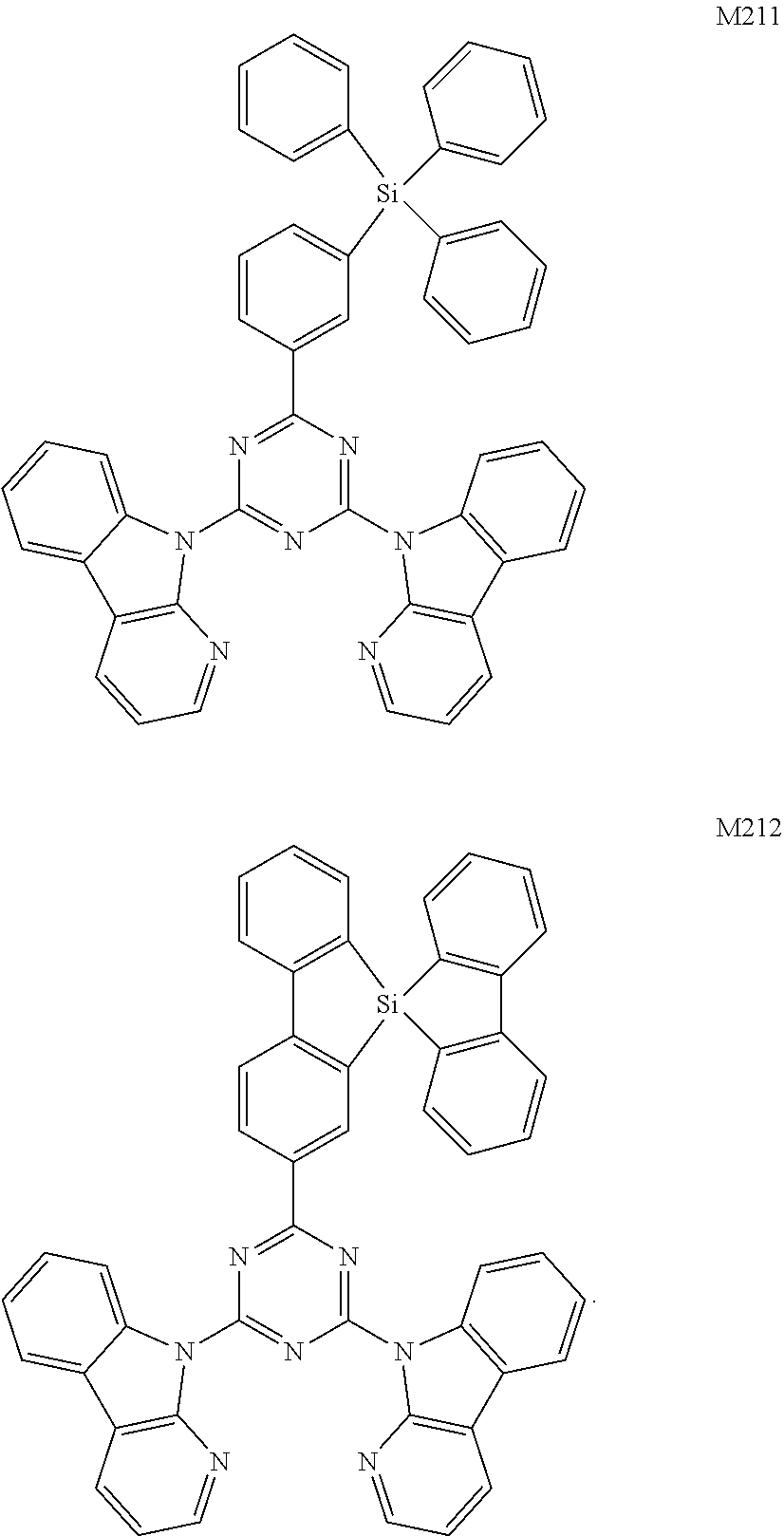
- the compound is any one of the following compounds:
- the present disclosure provides an electron transport material selected from the above-mentioned compounds which are capable of forming a tridentate or tetradentate complex structure with metal lithium, lithium organic complexes (for example, lithium 8-hydroxyquinolate), or metal Yb.
- the present disclosure provides a display panel including an organic light-emitting device (OLED device), the OLED device includes an anode, a cathode disposed oppositely to the anode, and an electron transport layer and a light-emitting layer disposed between the anode and the cathode, and the electron transport layer includes the compound of the present disclosure and a dopant selected from metal lithium, lithium organic complexes (for example, lithium 8-hydroxyquinolate), or metal Yb, so that the compound of the present disclosure forms a tridentate or tetradentate complex structure with the dopant in the electron transport layer.
- OLED device organic light-emitting device
- the OLED device includes an anode, a cathode disposed oppositely to the anode, and an electron transport layer and a light-emitting layer disposed between the anode and the cathode
- the electron transport layer includes the compound of the present disclosure and a dopant selected from metal lithium, lithium organic complexes (for example
- lithium 8-quinolinolate when lithium 8-quinolinolate is doped, lithium 8-quinolinolate is doped in mass ratio of 30%-70%, preferably 40%-60%, based on a total mass of the electron transport layer. In an embodiment, when lithium is doped, lithium is doped in mass ratio of 1.4%-3.4%, preferably 1.9%-2.9%, based on a total mass of the electron transport layer.
- the metal Yb when the metal Yb is doped, the metal Yb is doped in a mass ratio of 0.1%-10%, preferably 0.5%-5%, based on a total mass of the electron transport layer.
- the OLED device further includes a hole blocking layer, and the hole blocking layer is made of a material including the compound of the present disclosure.
- the OLED device further includes a first lamination layer and a second lamination layer disposed between the anode and the cathode and spaced apart from each other, and a charge generation layer (CGL) disposed between the first lamination layer and the second lamination layer and containing the compound of the present disclosure and a dopant selected from metal lithium, lithium organic complexes (for example, Liq and lithium 8-hydroxyquinolate), or metal Yb, so that the compound of the present disclosure forms a tridentate or tetradentate complex structure with the dopant in the charge generation layer (CGL).
- CGL charge generation layer
- Each of the first lamination layer and the second lamination layer includes a light-emitting layer
- the light-emitting layer of the first lamination layer includes a first light-emitting layer formed between the anode and the charge generation layer
- the light-emitting layer of the second lamination layer includes a second light-emitting layer formed between the cathode and the charge generation layer.
- lithium 8-quinolinolate is doped
- lithium 8-quinolinolate is doped in mass ratio of 30%-70%, preferably 40%-60%, based on a total mass of the charge generation layer.
- lithium is doped in mass ratio of 1.4%-3.4%, preferably 1.9%-2.9%, based on a total mass of the charge generation layer.
- the metal Yb is doped, in an embodiment, the metal Yb is doped in a mass ratio of 0.1%-10%, preferably 0.5%-5%, based on a total mass of the charge generation layer.
- the first light-emitting layer and the second light-emitting layer each are independently a mono-color light-emitting layer or a composite light-emitting layer formed by stacking a plurality of mono-color light-emitting layers
- the mono-color light-emitting layer is a red light-emitting layer, a green light-emitting layer, a blue light-emitting layer, or a yellow light-emitting layer
- each mono-color light-emitting layer of the plurality of mono-color light-emitting layers is independently a red light-emitting layer, a green light-emitting layer, a blue light-emitting layer, or a yellow light-emitting layer.
- the first light-emitting layer and the second light-emitting layer are independently selected from a fluorescent light-emitting layer or a phosphorescent light-emitting layer.
- the organic light-emitting device further includes one or more of a hole injection layer, a hole blocking layer, an electron injection layer, or an electron blocking layer.
- Materials used in these functional layers are not particularly limited, which can be selected according to actual conditions.
- the present disclosure further exemplarily describes synthesis of compounds M004, M037, M056, M104 and M157.
- X002 (1.15 mmol) was dissolved in 40 mL of anhydrous tetrahydrofuran (THF). NaH (1.4 mmol), after repeatedly washed with n-hexane, was added to the above solution. After stirring for 1 h, X001 (1.1 mmol) was added and stirred overnight at room temperature. The reaction was quenched by adding methanol and water and was extracted with dichloromethane. The organic phase was collected and dried over anhydrous Na 2 SO 4 . The dried solution was filtered, and the solvent was removed by using a rotary evaporator to obtain a crude product. The crude product was purified by silica gel chromatography using chloroform/n-hexane as eluent to obtain intermediate X003 (0.94 mmol, yield 85%).
- THF anhydrous tetrahydrofuran
- X004 (1.15 mmol) was dissolved in 45 mL of anhydrous THF. NaH (1.5 mmol), after repeatedly washed with n-hexane, was added to the above solution. After stirring for 1 h, X003 (1.0 mmol) was added and stirred overnight at room temperature. The reaction was quenched by adding methanol and water and was extracted with dichloromethane. The organic phase was collected and dried over anhydrous Na 2 SO 4 . The dried solution was filtered, and the solvent was removed by using a rotary evaporator to obtain a crude product. The crude product was purified by silica gel chromatography using chloroform/n-hexane as eluent to obtain intermediate X005 (0.78 mmol, yield 78%).
- the crude product was purified through a silica gel chromatography column, using a mixed solvent of n-hexane and chloroform with a volume ratio of 5:1 as eluent to finally obtain a solid M004 (0.88 mmol, yield 88%).
- X 010 (2.3 mmol) was dissolved in 60 mL of anhydrous THF. NaH (3.5 mmol), after repeatedly washed with n-hexane, was added to the above solution. After stirring for 1 h, X009 (1.0 mmol) was added and stirred overnight at room temperature. The reaction was quenched by adding methanol and water and was extracted with dichloromethane. The organic phase was collected and dried over anhydrous Na 2 SO 4 . The dried solution was filtered, and the solvent was removed by using a rotary evaporator to obtain a crude product. The crude product was purified by silica gel chromatography using chloroform/n-hexane as eluent to obtain target compound M056 (0.71 mmol, yield 71%).
- Elemental analysis calculated: C, 76.67; H, 3.65; N, 16.92; O, 2.76; measured: C, 76.70; H, 3.67; N, 16.89; O, 2.74.
- X010 (1.05 mmol) was dissolved in 40 mL of anhydrous THF. NaH (1.3 mmol), after repeatedly washed with n-hexane, was added to the above solution. After stirring for 1 h, X001 (1.0 mmol) was added and stirred overnight at room temperature. The reaction was quenched by adding methanol and water and was extracted with dichloromethane. The organic phase was collected and dried over anhydrous Na 2 SO 4 . The dried solution was filtered, and the solvent was removed by using a rotary evaporator to obtain a crude product. The crude product was purified by silica gel chromatography using chloroform/n-hexane as eluent to obtain intermediate X011 (0.81 mmol, yield 81%).
- X004 (1.6 mmol) was dissolved in 50 mL of anhydrous THF. NaH (1.9 mmol), after repeatedly washed with n-hexane, was added to the above solution. After stirring for 1 h, X011 (1.5 mmol) was added and stirred overnight at room temperature. The reaction was quenched by adding methanol and water and was extracted with dichloromethane. The organic phase was collected and dried over anhydrous Na 2 SO 4 . The dried solution was filtered, and the solvent was removed by using a rotary evaporator to obtain a crude product. The crude product was purified by silica gel chromatography using chloroform/n-hexane as eluent to obtain intermediate X012 (1.1 mmol, yield 73%).
- MALDI-TOF MS m/z calculated: C 30 H 25 BN 8 O 2 : 540.2; measured: 540.5.
- Elemental analysis calculated: C, 73.25; H, 3.66; N, 16.27; O, 2.32; measured: C, 73.24; H, 3.67; N, 16.26; O, 2.34.
- X004 (2.3 mmol) was dissolved in 60 mL of anhydrous THF. NaH (3.5 mmol), after repeatedly washed with n-hexane, was added to the above solution. After stirring for 1 h, X015 (1.0 mmol) was added and stirred overnight at room temperature. The reaction was quenched by adding methanol and water and was extracted with dichloromethane. The organic phase was collected and dried over anhydrous Na 2 SO 4 . The dried solution was filtered, and the solvent was removed by using a rotary evaporator to obtain a crude product. The crude product was purified by silica gel chromatography using chloroform/n-hexane as eluent to obtain target compound M157 (0.60 mmol, yield 60%).
- the distributions of the molecular frontier orbitals of HOMO and LUMO were optimized and calculated by applying a density functional theory (DFT) and using a Gaussian 09 software package (Gaussian Inc.) with B3LYP/6-31G(d) calculation level. Meanwhile, based on time-dependent density functional theory (TDDFT), the lowest triplet energy level En of the molecules of the compounds was simulated and calculated. The results are shown in the following Table 1.
- DFT density functional theory
- Gaussian Inc. Gaussian 09 software package
- TDDFT time-dependent density functional theory
- the OLED device includes in sequence a substrate 1 , an ITO anode 2 , a hole injection layer 3 , a first hole transport layer 4 , a second hole transport layer 5 , a light-emitting layer 6 , a first electron transport layer 7 , a second electron transport layer 8 , and a cathode (silver electrode) 9 .
- the OLED device was manufactured by the following specific steps.
- a Keithley 2365A digital nanovoltmeter was used to measure the currents of the OLED devices at different voltages. The currents were divided by the light-emitting area to obtain current densities of the OLED device at the different voltages.
- Konicaminolta CS-2000 spectroradiometer was used to measure the brightness and the radiant energy flux density of the OLED devices at different voltages. According to the current densities and brightness of the OLED devices at different voltages, operating voltage (V) and a current efficiency (Cd/A) under the same current density (10 mA/cm 2 ) were obtained. Von was the turn-on voltage at a brightness of 1 cd/m 2 .
- the lifetime LT95 was obtained by measuring a lasting time period before the brightness of the organic light-emitting device was reduced to 95% of an initial brightness (measured at 50 mA/cm 2 ). Test data are listed in Table 2.
- Device Example 2 was the same as Device Example 1 in terms of manufacturing methods for respective layers and of the materials as used, except that M004 in step (7) was replaced with M016.
- Device Example 3 was the same as Device Example 1 in terms of manufacturing methods for respective layers and of the materials as used, except that M004 in step (7) was replaced with M020.
- Device Example 4 was the same as Device Example 1 in terms of manufacturing methods for respective layers and of the materials as used, except that M004 in step (7) was replaced with M037.
- Device Example 5 was the same as Device Example 1 in terms of manufacturing methods for respective layers and of the materials as used, except that M004 in step (7) was replaced with M044.
- Device Example 6 was the same as Device Example 1 in terms of manufacturing methods for respective layers and of the materials as used, except that M004 in step (7) was replaced with M056.
- Device Example 7 was the same as Device Example 1 in terms of manufacturing methods for respective layers and of the materials as used, except that M004 in step (7) was replaced with M104.
- Device Example 8 was the same as Device Example 1 in terms of manufacturing methods for respective layers and of the materials as used, except that M004 in step (7) was replaced with M124.
- Device Example 9 was the same as Device Example 1 in terms of manufacturing methods for respective layers and of the materials as used, except that M004 in step (7) was replaced with M128.
- Device Example 10 was the same as Device Example 1 in terms of manufacturing method for respective layers and of the materials as used, except that M004 in step (7) was replaced with M136.
- Device Example 11 was the same as Device Example 1 in terms of manufacturing methods for respective layers and of the materials as used, except that M004 in step (7) was replaced with M140.
- Device Example 12 was the same as Device Example 1 in terms of manufacturing methods for respective layers and of the materials as used, except that M004 in step (7) was replaced with M144.
- Device Example 13 was the same as Device Example 1 in terms of manufacturing methods for respective layers and of the materials as used, except that M004 in step (7) was replaced with M157.
- Device Example 14 was the same as Device Example 1 in terms of manufacturing methods for respective layers and of the materials as used, except that M004 in step (7) was replaced with M201.
- Device Example 15 was the same as Device Example 1 in terms of manufacturing methods for respective layers and of the materials as used, except that M004 in step (7) was replaced with M202.
- Device Comparative Example 1 was the same as Device Example 1 in terms of manufacturing methods for respective layers and of the materials as used, except that M004 in step (7) was replaced with Comparative Compound 1.
- Device Comparative Example 2 was the same as Device Example 1 in terms of manufacturing methods for respective layers and of the materials as used, except that M004 in step (7) was replaced with Comparative Compound 2.
- a Keithley 2365A digital nanovoltmeter was used to measure the currents of the OLED at different voltages. The currents were divided by the light-emitting area to calculate current densities of the OLED device at the different voltages.
- Konicaminolta CS-2000 spectroradiometer was used to measure the brightness and the radiant energy flux density of the OLED devices at different voltages. According to the current densities and brightness of the OLED devices at different voltages, a current efficiency CE (Cd/A) and operating voltage (V) of respective devices under the same current density (10 mA/cm 2 ) were obtained. Von was the turn-on voltage at a brightness of 1 cd/m 2 .
- the lifetime LT95 was obtained by measuring a lasting time period before the brightness of the organic light-emitting device was reduced to 95% of an initial brightness (measured at 50 mA/cm 2 ). Test results are listed in Table 2.
- the triazine skeleton structure cooperates with multiple substituents having large steric hindrance, so that the organic compound has large rigid twist, and avoids or reduces the increase in intermolecular attraction resulting from the excessively planar structure of conventional triazine compounds.
- the organic compounds of the present disclosure have a spatial structure and an appropriate molecular weight in the range of 600-1200 g/mol suitable to control the evaporation rate and inhibit the accumulation caused by the increase of intermolecular attraction. These factors work together to lower the turn-on voltage of the OLED device, reduce the operating voltage of the OLED device, and improve the efficiency of the OLED device while prolonging the lifetime.
- the compounds of the present disclosure can also be used in the charge generation layer (CGL) in laminate OLED devices.
- CGL charge generation layer
- the use of the compound of the present disclosure in the charge generation layer will be described below in detail.
- this example provides a laminate OLED device.
- the organic light-emitting device includes in sequence a substrate 1 ′, an anode 2 ′, a hole injection layer 3 ′, a first hole transport layer 4 ′, a first light-emitting layer 5 ′, a first electron transport layer 6 ′, an n-type charge generation layer 7 ′, a p-type charge generation layer 8 ′, a second hole transport layer 9 ′, a second light-emitting layer 101 ′, a second electron transport layer 11 ′, an electron injection layer 12 ′, and a cathode 13 ′.
- the OLED device was manufactured by the following specific steps.
- this example provides a laminate OLED device.
- the OLED device includes in sequence a substrate 1 ′, an anode 2 ′, a hole injection layer 3 ′, a first hole transport layer 4 ′, a first light-emitting layer 5 ′, a first electron transport layer 6 ′, an n-type charge generation layer 7 ′, a p-type charge generation layer 8 ′, a second hole transport layer 9 ′, a second light-emitting layer 102 ′, a third light-emitting layer 103 ′, a second electron transport layer 11 ′, an electron injection layer 12 ′, and a cathode 13 ′.
- the OLED device was manufactured by the following specific steps.
- Table 3 shows the test results for the light-emitting performance of the devices in Device Example 16 and Device Example 17.
- the compounds of the present disclosure can be doped with metal Yb to form an n-type charge generation layer.
- two blue light-emitting layers are arranged in series to provide a blue light-emitting device having a current efficiency of up to 11.2 cd/A.
- a blue light-emitting layer, a red light-emitting layer and a green light-emitting layer are arranged in series to provide a white light-emitting device having a current efficiency of up to 60.3 cd/A, indicating that the compounds of the present disclosure are excellent n-type CGL material suitable for the CGL material in laminate OLED devices.
- Another aspect of the present disclosure further provides a display apparatus which includes the display panel as described above.
- the display apparatus can be a display screen of a mobile phone, a computer, a TV, a smart watch, a smart car, a VR or AR helmet, or any other smart devices.
- FIG. 5 is a schematic diagram of a display apparatus according to an embodiment of the present disclosure, e.g., a smartphone 30 .
- the display apparatus includes the display panel 20 of the embodiment of the present disclosure.
Landscapes
- Chemical & Material Sciences (AREA)
- Organic Chemistry (AREA)
- Physics & Mathematics (AREA)
- Materials Engineering (AREA)
- Engineering & Computer Science (AREA)
- Spectroscopy & Molecular Physics (AREA)
- Optics & Photonics (AREA)
- Life Sciences & Earth Sciences (AREA)
- Molecular Biology (AREA)
- General Health & Medical Sciences (AREA)
- Biochemistry (AREA)
- Health & Medical Sciences (AREA)
- Electroluminescent Light Sources (AREA)
Abstract

Description


-
- wherein X1-X4 are each independently selected from a carbon atom or a nitrogen atom, and at least two of X1-X4 are each a nitrogen atom;
- R1-R4 are each independently absent or selected from the group consisting of a hydrogen atom, a C1-C20 alkyl group, a C1-C20 alkoxy group, a C1-C20 alkylthio group, a C1-C20 alkylamino group, a C6-C30 aryl group, and a C2-C30 heteroaryl group;
- m is 1 or 2;
- n and q are each independently selected from 0, 1, or 2, n+q≥1, and m+n+q=3; and
- Ar is a C6-C30 aryl group.

-
- in which, X1-X4 are each independently selected from a carbon atom or a nitrogen atom, and at least two of X1-X4 are each a nitrogen atom;
- R1-R4 are each independently absent or selected from the group consisting of a hydrogen atom, a C1-C20 alkyl group, a C1-C20 alkoxy group, a C1-C20 alkylthio group, a C1-C20 alkylamino group, a C6-C30 aryl group, and a C2-C30 heteroaryl group;
- m is an integer selected from 1 or 2;
- n and q are each integers independently selected from 0, 1, or 2, n+q≥1, and m+n+q=3; and
- Ar is a C6-C30 aryl group.


-
- in which, R5 and R6 are each independently absent or selected from the group consisting of a hydrogen atom, a C1-C20 alkyl group, a C1-C20 alkoxy group, a C1-C20 alkylthio group, a C1-C20 alkylamino group, a C6-C30 aryl group, and a C2-C30 heteroaryl group;
- R5 and R6 are capable of forming a ring;
- Y is selected from the group consisting of a carbon atom, an oxygen atom, a sulfur atom, a boron atom, a phosphorus atom, a P═O group, a silicon atom, and a germanium atom; and when Y is selected from an oxygen atom or a sulfur atom, R5 and R6 are absent;
- Q is selected from a carbon atom or a nitrogen atom; and
- * indicates a possible bonding position.

-
- in which, * indicates a possible bonding position.

-
- * indicates a possible bonding position.

-
- in which * indicates a possible bonding position.


| TABLE 1 | ||||
| Compound | HOMO (eV) | LUMO (eV) | Eg (eV) | ET1 (eV) |
| M004 | −5.64 | −1.77 | 3.87 | 2.67 |
| M016 | −5.65 | −1.87 | 3.78 | 2.81 |
| M020 | −5.66 | −1.90 | 3.76 | 2.80 |
| M037 | −5.50 | −2.05 | 3.45 | 2.65 |
| M044 | −5.71 | −1.77 | 3.94 | 2.67 |
| M056 | −5.89 | −1.85 | 4.04 | 2.81 |
| M104 | −5.88 | −2.05 | 3.83 | 2.64 |
| M124 | −5.60 | −1.67 | 3.93 | 2.66 |
| M128 | −5.74 | −1.70 | 4.04 | 2.65 |
| M136 | −5.95 | −1.76 | 4.19 | 2.79 |
| M140 | −5.78 | −1.78 | 4.00 | 2.78 |
| M144 | −6.12 | −1.96 | 4.16 | 2.64 |
| M157 | −6.04 | −1.95 | 4.09 | 2.64 |
| M201 | −5.80 | −1.73 | 4.07 | 2.61 |
| M202 | −6.19 | −1.59 | 4.60 | 3.14 |
| Comparative | −5.98 | −1.47 | 4.51 | 2.72 |
| compound 1 | ||||
| Comparative | −5.73 | −1.90 | 3.83 | 2.68 |
| |
||||
-
- (1) A glass substrate 1 was cut into a size of 50 mm×50 mm×0.7 mm, ultrasonically treated respectively in acetone, isopropanol and deionized water for 30 min, and then cleaned in ozone for 10 min; and the obtained glass substrate with an
ITO anode layer 2 was mounted on a vacuum deposition apparatus. - (2) Under a vacuum degree of 2×10⁻⁶ Pa, compound A used as a hole injection material was vacuum-evaporated onto the
ITO anode 2 to form a hole injection layer 3 having a thickness of 5 nm. - (3) Compound B was vacuum-evaporated on the hole injection layer 3 to form a first
hole transport layer 4 having a thickness of 90 nm. - (4) Compound C was vacuum-evaporated on the first
hole transport layer 4 to form a secondhole transport layer 5 having a thickness of 10 nm. - (5) A light-emitting
layer 6 having a thickness of 30 nm was formed by vacuum evaporation on the secondhole transport layer 5, where compound D was used as the host of the light-emittinglayer 6, and compound E was used as the dopant of the light-emittinglayer 6, with a doping ratio being 3% by weight. - (6) Compound F was vacuum-evaporated on the light-emitting
layer 6 to form a firstelectron transport layer 7 having a thickness of 5 nm. - (7) Compound M004 provided by the present disclosure and doping metal ytterbium (the mass ratio was 97:3) were vacuum-evaporated on the first
electron transport layer 7 to form a secondelectron transport layer 8 having a thickness of 30 nm. - (8) Silver was vacuum-evaporated on the second
electron transport layer 8 to form acathode 9 having a thickness of 100 nm.
- (1) A glass substrate 1 was cut into a size of 50 mm×50 mm×0.7 mm, ultrasonically treated respectively in acetone, isopropanol and deionized water for 30 min, and then cleaned in ozone for 10 min; and the obtained glass substrate with an


Performance Evaluation of OLED Devices:


Performance Evaluation of OLED Devices
| TABLE 2 |
| Test Results of Device Examples and Device Comparative Examples |
| Compounds | ||||||
| used | ||||||
| as electron | ||||||
| transport | V | EC | Lifetime | |||
| OLED device | material | Von (V) | (V) | (cd/A) | LT95 (h) | |
| Device Example 1 | M004 | 2.67 | 3.97 | 6.70 | 70 | |
| Device Example 2 | M016 | 2.67 | 3.99 | 6.82 | 72 | |
| Device Example 3 | M020 | 2.68 | 3.98 | 6.75 | 74 | |
| Device Example 4 | M037 | 2.74 | 4.03 | 6.34 | 65 | |
| Device Example 5 | M044 | 2.66 | 3.96 | 6.68 | 69 | |
| Device Example 6 | M056 | 2.68 | 4.00 | 6.85 | 72 | |
| Device Example 7 | M104 | 2.72 | 4.02 | 6.39 | 62 | |
| Device Example 8 | M124 | 2.65 | 3.97 | 6.78 | 72 | |
| Device Example 9 | M128 | 2.69 | 4.00 | 6.65 | 66 | |
| Device Example 10 | M136 | 2.66 | 3.96 | 6.80 | 73 | |
| Device Example 11 | M140 | 2.67 | 3.99 | 6.72 | 70 | |
| Device Example 12 | M144 | 2.75 | 4.04 | 6.36 | 65 | |
| Device Example 13 | M157 | 2.73 | 4.03 | 6.30 | 68 | |
| Device Example 14 | M201 | 2.70 | 3.98 | 6.58 | 69 | |
| Device Example 15 | M202 | 2.69 | 3.96 | 6.64 | 68 | |
| Device | Comparative | 2.86 | 4.14 | 5.40 | 44 | |
| Comparative | Compound 1 | |||||
| Example 1 | ||||||
| Device | Comparative | 2.81 | 4.15 | 5.16 | 48 | |
| | Compound | 2 | ||||
| Example 2 | ||||||
-
- (1) A glass substrate 1′ was cut into a size of 50 mm×50 mm×0.7 mm, ultrasonically treated respectively in acetone, isopropanol and deionized water for 30 min, and then cleaned in ozone for 10 min; and the obtained glass substrate with an
ITO anode layer 2′ was mounted on a vacuum deposition apparatus. - (2) Under a vacuum degree of 2×10⁻⁶ Pa, compound A used as a hole injection material was vacuum-evaporated onto the
ITO anode 2′ to form a first hole injection layer 3′ having a thickness of 5 nm. - (3) Compound B was vacuum-evaporated on the first hole injection layer 3′ to form a first
hole transport layer 4′ having a thickness of 90 nm. - (4) A first light-emitting
layer 5′ having a thickness of 30 nm was vacuum-evaporated on the firsthole transport layer 4′, where compound D was used as the host of the first light-emittinglayer 5′, and compound E was used as the dopant (a blue light material) of the light-emittinglayer 5′, with a doping ratio being 3% by weight. - (5) Compound G was vacuum-evaporated on the first light-emitting
layer 5′ to form a firstelectron transport layer 6′ having a thickness of 35 nm. - (6) The organic compound M004 of the present disclosure and metal ytterbium (mass ratio of the two was 97:3) were vacuum-evaporated on the first
electron transport layer 6′ to form an n-typecharge generation layer 7′ having a thickness of 5 nm. - (7) Compound A used as a hole injection material was vacuum-evaporated on the n-type
charge generation layer 7′ to form a p-typecharge generation layer 8′ having a thickness of 5 nm. - (8) Compound B was vacuum-evaporated on the p-type
charge generation layer 8′ to form a secondhole transport layer 9′ having a thickness of 90 nm. - (9) A second light-emitting
layer 101′ having a thickness of 30 nm was vacuum-evaporated on the secondhole transport layer 9′, where compound D was used as the host of the second light-emittinglayer 101′, and compound E was used as the dopant (a blue light material) of the second light-emittinglayer 101′, with a doping ratio being 3% by weight. - (10) Compound F was vacuum-evaporated on the second light-emitting
layer 101′ to form a second electron transport layer 11′ having a thickness of 5 nm. - (11) Compound G and Liq (weight ratio of the two was 50:50) were vacuum-evaporated on the second electron transport layer 11′ to form an
electron injection layer 12′ having a thickness of 35 nm. - (12) Silver was vacuum-evaporated on the
electron injection layer 12′ to form acathode 13′ having a thickness of 100 nm.
- (1) A glass substrate 1′ was cut into a size of 50 mm×50 mm×0.7 mm, ultrasonically treated respectively in acetone, isopropanol and deionized water for 30 min, and then cleaned in ozone for 10 min; and the obtained glass substrate with an


-
- (1) A glass substrate 1′ was cut into a size of 50 mm×50 mm×0.7 mm, ultrasonically treated respectively in acetone, isopropanol and deionized water for 30 min, and then cleaned in ozone for 10 min; and the obtained glass substrate with an
ITO anode layer 2′ was mounted on a vacuum deposition apparatus. - (2) Under a vacuum degree of 2×10⁻⁶ Pa, a hole injection material of compound A was vacuum-evaporated onto the
ITO anode 2′ to form a first hole injection layer 3′ having a thickness of 5 nm. - (3) Compound B was vacuum-evaporated on the first hole injection layer 3′ to form a first
hole transport layer 4′ having a thickness of 90 nm. - (4) A first light-emitting
layer 5′ having a thickness of 30 nm was vacuum-evaporated on the firsthole transport layer 4′, where compound D was used as the host of the first light-emittinglayer 5′, and compound E was used as the dopant (a blue light material) of the light-emittinglayer 5′, with a doping ratio being 3% by weight. - (5) Compound G was vacuum-evaporated on the first light-emitting
layer 5′ to form a firstelectron transport layer 6′ having a thickness of 35 nm. - (6) The organic compound M004 of the present disclosure and metal ytterbium (mass ratio of the two was 97:3) were vacuum-evaporated on the first
electron transport layer 6′ to form an n-typecharge generation layer 7′ having a thickness of 5 nm. - (7) Compound A used as a hole injection material was vacuum-evaporated on the n-type
charge generation layer 7′ to form a p-typecharge generation layer 8′ having a thickness of 5 nm. - (8) Compound B was vacuum-evaporated on the p-type
charge generation layer 8′ to form a secondhole transport layer 9′ having a thickness of 90 nm. - (9) A second light-emitting
layer 102′ having a thickness of 30 nm was formed by vacuum-evaporation on the secondhole transport layer 9′, where compound H was used as the host of the second light-emittinglayer 102′, and compound I was used as the dopant (a green light material) of the second light-emittinglayer 102′, with a doping ratio being 8% by weight; a third light-emittinglayer 103′ having a thickness of 30 nm was formed by vacuum-evaporation on the second light-emittinglayer 102′, where compound H was used as the host of the third light-emittinglayer 103′, and compound J was used as the dopant (a red light material) of the third light-emittinglayer 103′, with a doping ratio being 8% by weight; - (10) Compound F was vacuum-evaporated on the third light-emitting
layer 103′ to form a second electron transport layer 11′ having a thickness of 5 nm. - (11) Compound G and Liq (weight ratio of the two was 50:50) were vacuum-evaporated on the second electron transport layer 11′ to form an
electron injection layer 12′ having a thickness of 35 nm. - (12) Silver was vacuum-evaporated on the
electron injection layer 12′ to form acathode 13′ having a thickness of 100 nm.
- (1) A glass substrate 1′ was cut into a size of 50 mm×50 mm×0.7 mm, ultrasonically treated respectively in acetone, isopropanol and deionized water for 30 min, and then cleaned in ozone for 10 min; and the obtained glass substrate with an

| TABLE 3 | |||||
| Current | |||||
| Compound used in | efficiency | ||||
| OLED device | CGL | V (V) | (cd/A) | ||
| Device Example | M004 | 7.4 | 11.2 | ||
| 16 | |||||
| Device Example | M004 | 8.2 | 60.3 | ||
| 17 | |||||
Claims (15)


Applications Claiming Priority (2)
| Application Number | Priority Date | Filing Date | Title |
|---|---|---|---|
| CN202011193784.6 | 2020-10-30 | ||
| CN202011193784.6A CN112300162B (en) | 2020-10-30 | 2020-10-30 | Compound, electron transport material, display panel, and display device |
Publications (2)
| Publication Number | Publication Date |
|---|---|
| US20210130355A1 US20210130355A1 (en) | 2021-05-06 |
| US12134615B2 true US12134615B2 (en) | 2024-11-05 |
Family
ID=74333091
Family Applications (1)
| Application Number | Title | Priority Date | Filing Date |
|---|---|---|---|
| US17/147,085 Active 2043-03-30 US12134615B2 (en) | 2020-10-30 | 2021-01-12 | Compound, electron transport material, display panel and display apparatus |
Country Status (2)
| Country | Link |
|---|---|
| US (1) | US12134615B2 (en) |
| CN (2) | CN112300162B (en) |
Families Citing this family (7)
| Publication number | Priority date | Publication date | Assignee | Title |
|---|---|---|---|---|
| KR102921530B1 (en) * | 2020-12-31 | 2026-02-03 | 엘지디스플레이 주식회사 | Organic Light Emitting Device and Display Device Using the Same |
| KR20220100132A (en) * | 2021-01-07 | 2022-07-15 | 삼성디스플레이 주식회사 | Light emitting device and electronic apparatus including the same |
| JP2023067419A (en) * | 2021-11-01 | 2023-05-16 | エスケーマテリアルズジェイエヌシー株式会社 | polycyclic aromatic compound |
| CN116120308B (en) * | 2021-11-12 | 2025-11-07 | 奥来德(上海)光电材料科技有限公司 | Nitrogen-containing heterocyclic compound taking phenanthroline as parent nucleus, and preparation method and application thereof |
| KR102949076B1 (en) * | 2021-12-31 | 2026-04-08 | 엘지디스플레이 주식회사 | Light Emitting Device and Light Display Device Using the Same |
| US20230217821A1 (en) * | 2021-12-31 | 2023-07-06 | Lg Display Co., Ltd. | Light Emitting Device and Light Emitting Display Device Including the Same |
| CN118420653A (en) * | 2023-02-01 | 2024-08-02 | 陕西莱特光电材料股份有限公司 | Organic compound, organic electroluminescent device and electronic device |
Citations (10)
| Publication number | Priority date | Publication date | Assignee | Title |
|---|---|---|---|---|
| US20110095282A1 (en) * | 2008-12-22 | 2011-04-28 | Merck Patent Gmbh | Organic electroluminescent device comprising triazine derivatives |
| KR20150124637A (en) | 2014-04-29 | 2015-11-06 | (주)피엔에이치테크 | An electroluminescent compound and an electroluminescent device comprising the same |
| US20160155959A1 (en) * | 2013-07-02 | 2016-06-02 | Merck Patent Gmbh | Organic Electroluminescent Device |
| CN106986870A (en) | 2016-07-15 | 2017-07-28 | 机光科技股份有限公司 | Organic electric field color changing device and o-diazaphenanthrene based compound used for the same |
| KR20180063708A (en) | 2016-12-02 | 2018-06-12 | (주)피엔에이치테크 | An electroluminescent compound and an electroluminescent device comprising the same |
| CN108424420A (en) * | 2017-09-30 | 2018-08-21 | 北京绿人科技有限责任公司 | Triaizine compounds containing silicon atom and its application and a kind of organic electroluminescence device |
| US20190198790A1 (en) * | 2017-12-22 | 2019-06-27 | Lg Display Co., Ltd. | Organic light-emitting diode, organic light-emitting display including the same, and method of manufacturing the same |
| US20190305227A1 (en) * | 2018-03-28 | 2019-10-03 | Lg Display Co., Ltd. | Novel organic compounds and organic electroluminescent device including the same |
| WO2020091521A1 (en) | 2018-11-02 | 2020-05-07 | 주식회사 엘지화학 | Compound and organic light emitting device comprising same |
| CN111224005A (en) | 2018-11-26 | 2020-06-02 | 三星显示有限公司 | Heterocyclic compound and organic light-emitting device including the same |
Family Cites Families (5)
| Publication number | Priority date | Publication date | Assignee | Title |
|---|---|---|---|---|
| KR20180028179A (en) * | 2016-09-08 | 2018-03-16 | 에스케이케미칼 주식회사 | Compound for organic electroluminescent device and organic electroluminescent device comprising the same |
| KR102487503B1 (en) * | 2017-07-04 | 2023-01-12 | 솔루스첨단소재 주식회사 | Organic compound and organic electroluminescent device using the same |
| KR102530155B1 (en) * | 2017-10-23 | 2023-05-10 | 솔루스첨단소재 주식회사 | Organic compounds and organic electro luminescence device comprising the same |
| US20200020867A1 (en) * | 2018-07-13 | 2020-01-16 | Universal Display Corporation | Organic electroluminescent materials and devices |
| KR102312963B1 (en) * | 2018-12-26 | 2021-10-14 | 엘티소재주식회사 | Compound, composition and organic optoelectronic device and display device |
-
2020
- 2020-10-30 CN CN202011193784.6A patent/CN112300162B/en active Active
- 2020-10-30 CN CN202210236266.0A patent/CN114560858B/en active Active
-
2021
- 2021-01-12 US US17/147,085 patent/US12134615B2/en active Active
Patent Citations (10)
| Publication number | Priority date | Publication date | Assignee | Title |
|---|---|---|---|---|
| US20110095282A1 (en) * | 2008-12-22 | 2011-04-28 | Merck Patent Gmbh | Organic electroluminescent device comprising triazine derivatives |
| US20160155959A1 (en) * | 2013-07-02 | 2016-06-02 | Merck Patent Gmbh | Organic Electroluminescent Device |
| KR20150124637A (en) | 2014-04-29 | 2015-11-06 | (주)피엔에이치테크 | An electroluminescent compound and an electroluminescent device comprising the same |
| CN106986870A (en) | 2016-07-15 | 2017-07-28 | 机光科技股份有限公司 | Organic electric field color changing device and o-diazaphenanthrene based compound used for the same |
| KR20180063708A (en) | 2016-12-02 | 2018-06-12 | (주)피엔에이치테크 | An electroluminescent compound and an electroluminescent device comprising the same |
| CN108424420A (en) * | 2017-09-30 | 2018-08-21 | 北京绿人科技有限责任公司 | Triaizine compounds containing silicon atom and its application and a kind of organic electroluminescence device |
| US20190198790A1 (en) * | 2017-12-22 | 2019-06-27 | Lg Display Co., Ltd. | Organic light-emitting diode, organic light-emitting display including the same, and method of manufacturing the same |
| US20190305227A1 (en) * | 2018-03-28 | 2019-10-03 | Lg Display Co., Ltd. | Novel organic compounds and organic electroluminescent device including the same |
| WO2020091521A1 (en) | 2018-11-02 | 2020-05-07 | 주식회사 엘지화학 | Compound and organic light emitting device comprising same |
| CN111224005A (en) | 2018-11-26 | 2020-06-02 | 三星显示有限公司 | Heterocyclic compound and organic light-emitting device including the same |
Non-Patent Citations (3)
| Title |
|---|
| First Office Action mailed May 28, 2021, in corresponding Chinese Patent Application No. 202011193784.6, 126 pages (with English translation). |
| Machine translation for CN 108424420 A (publication date Aug. 2018). (Year: 2018). * |
| Youn, Kyu Man, et al. "Blue thermally activated delayed fluorescence emitters with a δ-pyridoindole donor moiety." New Journal of Chemistry 42.7 (2018): 5532-5539. (Year: 2018). * |
Also Published As
| Publication number | Publication date |
|---|---|
| CN112300162A (en) | 2021-02-02 |
| CN114560858B (en) | 2023-04-07 |
| CN114560858A (en) | 2022-05-31 |
| CN112300162B (en) | 2022-04-05 |
| US20210130355A1 (en) | 2021-05-06 |
Similar Documents
| Publication | Publication Date | Title |
|---|---|---|
| US12134615B2 (en) | Compound, electron transport material, display panel and display apparatus | |
| US9711742B2 (en) | Four coordinated platinum and palladium complexes with geometrically distorted charge transfer state and their applications in light emitting devices | |
| Tao et al. | Highly efficient blue phosphorescent iridium (III) complexes with various ancillary ligands for partially solution-processed organic light-emitting diodes | |
| US10263197B2 (en) | Synthesis of four coordinated palladium complexes and their applications in light emitting devices thereof | |
| CN105980518B (en) | Compound and organic electronic device | |
| US8859109B2 (en) | Compound for organic electroluminescent device and organic electroluminescent device using the same | |
| US20100102710A1 (en) | Novel organic electroluminescent compounds and organic electroluminescent device using the same | |
| US7723520B2 (en) | Red electroluminescent compounds and organic electroluminescent device using the same | |
| US20090295281A1 (en) | Novel organic electroluminescent compounds and organic electroluminescent device using the same | |
| CN106661070A (en) | Metal complexes | |
| KR20130110934A (en) | Organometallic compounds and organic light emitting diodes comprising the compounds | |
| US11201296B2 (en) | Compounds having fluorene structures | |
| US20090260686A1 (en) | Novel organic electroluminescent compounds and organic electroluminescent device using the same | |
| CN111675701B (en) | An organic electroluminescent compound and organic electroluminescent device based on triphenylamine structure | |
| US20190106391A1 (en) | Compounds with spirobifluorene-structures | |
| KR101558966B1 (en) | Asymmetric ortho-Terphenyl Derivatives and Organic light emitting device Comprising the Same | |
| WO2018230860A1 (en) | Novel compound and organic light emitting device comprising same | |
| CN104326980A (en) | 9,9'- connected host material based on 4,4'-difluorene structure and application thereof | |
| US20200270280A1 (en) | Organic compound, an electron transport material and an application thereof | |
| CN109053690B (en) | Bipolar Electroluminescent Materials Containing Carbazole Groups and Their Applications | |
| US20250107433A1 (en) | Fluorene-containing heterocyclic compound and organic electroluminescent device thereof | |
| CN115244060A (en) | Material for organic electroluminescent device | |
| CN120795038A (en) | Iridium-containing metal heterocycle phosphorescence doping material and organic electroluminescent device | |
| US20250113725A1 (en) | Platinum complex and organic photoelectronic device comprising the same | |
| KR101771530B1 (en) | Organic metal compounds and organic light emitting diodes comprising the same |
Legal Events
| Date | Code | Title | Description |
|---|---|---|---|
| AS | Assignment |
Owner name: SHANGHAI TIANMA AM-OLED CO., LTD., CHINA Free format text: ASSIGNMENT OF ASSIGNORS INTEREST;ASSIGNORS:GAO, WEI;ZHAI, LU;ZHANG, LEI;AND OTHERS;REEL/FRAME:054894/0813 Effective date: 20201222 |
|
| FEPP | Fee payment procedure |
Free format text: ENTITY STATUS SET TO UNDISCOUNTED (ORIGINAL EVENT CODE: BIG.); ENTITY STATUS OF PATENT OWNER: LARGE ENTITY |
|
| STPP | Information on status: patent application and granting procedure in general |
Free format text: APPLICATION DISPATCHED FROM PREEXAM, NOT YET DOCKETED |
|
| STPP | Information on status: patent application and granting procedure in general |
Free format text: DOCKETED NEW CASE - READY FOR EXAMINATION |
|
| AS | Assignment |
Owner name: WUHAN TIANMA MICROELECTRONICS CO., LTD. SHANGHAI BRANCH, CHINA Free format text: ASSIGNMENT OF ASSIGNORS INTEREST;ASSIGNOR:SHANGHAI TIANMA AM-OLED CO.,LTD.;REEL/FRAME:059498/0307 Effective date: 20220301 Owner name: WUHAN TIANMA MICRO-ELECTRONICS CO., LTD., CHINA Free format text: ASSIGNMENT OF ASSIGNORS INTEREST;ASSIGNOR:SHANGHAI TIANMA AM-OLED CO.,LTD.;REEL/FRAME:059498/0307 Effective date: 20220301 |
|
| STPP | Information on status: patent application and granting procedure in general |
Free format text: NON FINAL ACTION MAILED |
|
| STPP | Information on status: patent application and granting procedure in general |
Free format text: RESPONSE TO NON-FINAL OFFICE ACTION ENTERED AND FORWARDED TO EXAMINER |
|
| STPP | Information on status: patent application and granting procedure in general |
Free format text: FINAL REJECTION MAILED |
|
| STPP | Information on status: patent application and granting procedure in general |
Free format text: ADVISORY ACTION MAILED |
|
| STPP | Information on status: patent application and granting procedure in general |
Free format text: DOCKETED NEW CASE - READY FOR EXAMINATION |
|
| STPP | Information on status: patent application and granting procedure in general |
Free format text: NOTICE OF ALLOWANCE MAILED -- APPLICATION RECEIVED IN OFFICE OF PUBLICATIONS |
|
| ZAAB | Notice of allowance mailed |
Free format text: ORIGINAL CODE: MN/=. |
|
| STPP | Information on status: patent application and granting procedure in general |
Free format text: PUBLICATIONS -- ISSUE FEE PAYMENT VERIFIED |
|
| STCF | Information on status: patent grant |
Free format text: PATENTED CASE |