US12132147B2 - Patterned substrate for light-emitting diode - Google Patents
Patterned substrate for light-emitting diode Download PDFInfo
- Publication number
- US12132147B2 US12132147B2 US17/876,546 US202217876546A US12132147B2 US 12132147 B2 US12132147 B2 US 12132147B2 US 202217876546 A US202217876546 A US 202217876546A US 12132147 B2 US12132147 B2 US 12132147B2
- Authority
- US
- United States
- Prior art keywords
- nodes
- concave
- links
- substrate
- sidewalls
- Prior art date
- Legal status (The legal status is an assumption and is not a legal conclusion. Google has not performed a legal analysis and makes no representation as to the accuracy of the status listed.)
- Active, expires
Links
Images


Classifications
-
- H01L33/20—
-
- H—ELECTRICITY
- H10—SEMICONDUCTOR DEVICES; ELECTRIC SOLID-STATE DEVICES NOT OTHERWISE PROVIDED FOR
- H10H—INORGANIC LIGHT-EMITTING SEMICONDUCTOR DEVICES HAVING POTENTIAL BARRIERS
- H10H20/00—Individual inorganic light-emitting semiconductor devices having potential barriers, e.g. light-emitting diodes [LED]
- H10H20/01—Manufacture or treatment
- H10H20/011—Manufacture or treatment of bodies, e.g. forming semiconductor layers
- H10H20/013—Manufacture or treatment of bodies, e.g. forming semiconductor layers having light-emitting regions comprising only Group III-V materials
- H10H20/0133—Manufacture or treatment of bodies, e.g. forming semiconductor layers having light-emitting regions comprising only Group III-V materials with a substrate not being Group III-V materials
- H10H20/01335—Manufacture or treatment of bodies, e.g. forming semiconductor layers having light-emitting regions comprising only Group III-V materials with a substrate not being Group III-V materials the light-emitting regions comprising nitride materials
-
- H01L33/06—
-
- H01L33/145—
-
- H01L33/32—
-
- H—ELECTRICITY
- H10—SEMICONDUCTOR DEVICES; ELECTRIC SOLID-STATE DEVICES NOT OTHERWISE PROVIDED FOR
- H10H—INORGANIC LIGHT-EMITTING SEMICONDUCTOR DEVICES HAVING POTENTIAL BARRIERS
- H10H20/00—Individual inorganic light-emitting semiconductor devices having potential barriers, e.g. light-emitting diodes [LED]
- H10H20/80—Constructional details
- H10H20/81—Bodies
- H10H20/811—Bodies having quantum effect structures or superlattices, e.g. tunnel junctions
- H10H20/812—Bodies having quantum effect structures or superlattices, e.g. tunnel junctions within the light-emitting regions, e.g. having quantum confinement structures
-
- H—ELECTRICITY
- H10—SEMICONDUCTOR DEVICES; ELECTRIC SOLID-STATE DEVICES NOT OTHERWISE PROVIDED FOR
- H10H—INORGANIC LIGHT-EMITTING SEMICONDUCTOR DEVICES HAVING POTENTIAL BARRIERS
- H10H20/00—Individual inorganic light-emitting semiconductor devices having potential barriers, e.g. light-emitting diodes [LED]
- H10H20/80—Constructional details
- H10H20/81—Bodies
- H10H20/816—Bodies having carrier transport control structures, e.g. highly-doped semiconductor layers or current-blocking structures
- H10H20/8162—Current-blocking structures
-
- H—ELECTRICITY
- H10—SEMICONDUCTOR DEVICES; ELECTRIC SOLID-STATE DEVICES NOT OTHERWISE PROVIDED FOR
- H10H—INORGANIC LIGHT-EMITTING SEMICONDUCTOR DEVICES HAVING POTENTIAL BARRIERS
- H10H20/00—Individual inorganic light-emitting semiconductor devices having potential barriers, e.g. light-emitting diodes [LED]
- H10H20/80—Constructional details
- H10H20/81—Bodies
- H10H20/819—Bodies characterised by their shape, e.g. curved or truncated substrates
- H10H20/82—Roughened surfaces, e.g. at the interface between epitaxial layers
-
- H—ELECTRICITY
- H10—SEMICONDUCTOR DEVICES; ELECTRIC SOLID-STATE DEVICES NOT OTHERWISE PROVIDED FOR
- H10H—INORGANIC LIGHT-EMITTING SEMICONDUCTOR DEVICES HAVING POTENTIAL BARRIERS
- H10H20/00—Individual inorganic light-emitting semiconductor devices having potential barriers, e.g. light-emitting diodes [LED]
- H10H20/80—Constructional details
- H10H20/81—Bodies
- H10H20/822—Materials of the light-emitting regions
- H10H20/824—Materials of the light-emitting regions comprising only Group III-V materials, e.g. GaP
- H10H20/825—Materials of the light-emitting regions comprising only Group III-V materials, e.g. GaP containing nitrogen, e.g. GaN
Definitions
- the present invention relates in general to semiconductor light emitting diode and, more particularly, to a patterned substrate used for light-emitting diode with improved optical output power efficiency.
- UV light-emitting diodes with optical emission wavelengths less than 360 nm are made of group-III nitride compound semiconductors such as AlGaN alloys.
- a typical UV LED includes an n-type AlGaN structure, a p-type AlGaN structure, and a light-emitting structure commonly made of AlGaN multiple-quantum-well (MQW) sandwiched in-between the n-type and p-type AlGaN structures.
- An AlGaN structure can be made of an AlGaN layer or many AlGaN layers joint forces to deliver a better function, such as to improve material quality, conductivity and/or carrier confinement.
- the Al-contents in the AlGaN layers/structures determines the optical emission wavelength of the LEDs.
- the optical emissions of wavelength less than 315 nm possess strong germicidal effect, making them ideal for food, water, air and surface disinfections.
- AlGaN being an optically dense material
- light generated in the AlGaN structures has small escape probabilities into free space due to total internal reflections. This has limited the light extraction efficiency for short wavelength UV LEDs to be as small as 16% even for a fully transparent deep UV LED structure (Jianping Zhang et al 2022 Semicond. Sci. Technol. 37 07LT01).
- the prior art patterned sapphire substrate designs have been done via intuitive approaches without well-outlined design principles. For GaN based visible LEDs these intuitive designs can work well as GaN has a high lateral growth rate which makes the smooth epitaxy coalescence readily achievable.
- AlN is the preferred growth template for UV LEDs in view of the opaqueness of GaN to most of the UV emissions. AlN has very small lateral growth rate for typical epitaxial temperatures (500-1400° C.).
- the disclosed pattern sapphire substrate designs require large film thickness to make AlN coalesce, usually more than 5 ⁇ m even more than 10 ⁇ m. These thick AlN layers can cause large wafer bowing which makes mass-production wafer processing very difficult if not impossible. Therefore, there is need to design patterned sapphire substrate for UV LEDs.
- the substrate includes a plurality of nodes and links protruding from a base plane of the substrate and base areas on the substrate, wherein each pair of adjacent nodes is connected by a corresponding link, respectively, and the base areas are defined and exposed by the nodes and the links, wherein:
- the substrate includes a plurality of concave nodes and concave links cutting into a surface of the substrate and base areas on the surface of the substrate, wherein each pair of adjacent concave nodes is connected by a corresponding concave link, respectively, wherein:
- This disclosure also provides a light emitting diode or a UV light emitting diode formed on the substrate described above.
- FIG. 1 illustrates an enlarged light escape cone for a patterned substrate as compared to a light escape cone for a flat substrate.
- FIG. 2 illustrates the effect of the size, thickness and thickness profile of a mask on the side wall profile of the formed pattern features on a patterned substrate.
- FIG. 3 illustrates a photolithography mask design M 1 to make patterned substrate according to an embodiment of the present disclosure.
- FIG. 4 compares the filling factors and perimeter ratios of masks according to mask design M 1 and a design from the prior art.
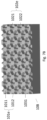
- FIG. 5 A illustrates a plan view of a portion of a patterned substrate made using a photolithography mask according to FIG. 3 .
- FIG. 5 B illustrates a perspective view of a patterned substrate shown in FIG. 5 A .
- FIG. 6 illustrates a photolithography mask design M 2 to make patterned substrate according to an embodiment of the present disclosure.
- FIG. 7 A illustrates a plan view of a portion of a patterned substrate made using a photolithography mask according to FIG. 6 .
- FIG. 7 B illustrates a perspective view of a patterned substrate shown in FIG. 7 A .
- FIG. 8 illustrates a photolithography mask design M 3 to make patterned substrate according to an embodiment of the present disclosure.
- FIG. 9 illustrates a photolithography mask design M 4 to make patterned substrate according to an embodiment of the present disclosure.
- FIG. 10 A illustrates a plan view of a portion of a patterned substrate made using a photolithography mask according to FIG. 9 .
- FIG. 10 B illustrates a perspective view of a patterned substrate shown in FIG. 10 A .
- FIG. 11 illustrates a UV LED epitaxial layered structure according to an embodiment of the present invention.
- group III nitride in general refers to metal nitride with cations selecting from group IIIA of the periodic table of the elements. That is to say, III-nitride includes AlN, GaN, InN and their ternary (AlGaN, InGaN, InAlN) and quaternary (AlInGaN) alloys.
- AlGaN, InGaN, InAlN ternary
- AlInGaN quaternary alloys.
- a quaternary can be reduced to a ternary for simplicity if one of the group III elements is significantly small so that its existence does not affect the intended function of a layer made of such material.
- a ternary AlInGaN For example, if the In-composition in a quaternary AlInGaN is significantly small, smaller than 1%, then this AlInGaN quaternary can be shown as ternary AlGaN for simplicity.
- a ternary can be reduced to a binary for simplicity if one of the group III elements is significantly small. For example, if the In-composition in a ternary InGaN is significantly small, smaller than 1%, then this InGaN ternary can be shown as binary GaN for simplicity.
- Group III nitride may also include small amount of transition metal nitride such as TiN, ZrN, HfN with molar fraction not larger than 10%.
- III-nitride or nitride may include Al x In y Ga z Ti (1-x-y-z) N, Al x In y Ga z Zr (1-x-y-z) N, Al x In y Ga z Hf (1-x-y-z) N, with (1-x-y-z) ⁇ 10%.
- light-emitting devices such as light-emitting diodes (LEDs) commonly adopt a light-emitting structure containing a quantum well active region, an n-type group III nitride structure for injecting electrons into the active region, and a p-type group III nitride structure on the other side of the active region for injecting holes into the active region.
- This light-emitting structure is generally formed over a transparent substrate. Even though being transparent to the light generated in the light-emitting structure, the substrate can be of different (usually smaller) optical refractive index.
- a base plane of a substrate is its main surface plane to receive epitaxial growth.
- the base plane of the substrate is usually a c-plane of sapphire.
- FIG. 1 illustrates a light-emitting structure formed over a transparent patterned substrate, containing many surface protrusions.
- the protrusions are made of the same material as that of the substrate, possessing sidewalls of angle of inclination cc with respect to the base plane of the substrate.
- a first aspect of the present disclosure is to optimize the inclination angle cc. First, consider light rays of angle of incidence ⁇ with respect to the base plane for
- the protrusions can maximize the light extraction efficiency for LEDs.
- the inclination angle of the protrusions with respect to the base plane is optionally to be within 35-55°, or 37-53°.
- the protrusion sidewall inclination angle ⁇ can be controlled and realized via etching (dry or wet) and photolithography mask selection.
- etching dry or wet
- photolithography mask selection to form etch patterns onto a substrate, a photolithography mask layer is formed on the substrate.
- the photolithography mask can protect the substrate materials beneath the mask during etching process.
- the substrate materials beneath the mask form a protrusion with sidewalls and the sidewalls are exposed and susceptible to lateral etching to form slanted sidewalls.
- the mask edge is also susceptible to lateral etching which will shrink the mask laterally and vertically.
- the mask thickness profile can also affect the protrusion sidewall inclination angle.
- FIG. 3 Shown in FIG. 3 is an illustrated plan view of a photolithography mask design M 1 according to one aspect of the present disclosure.
- mask M 1 geometrically is formed via translating a unit cell to fully cover a plane.
- the unit cell of mask M 1 is a rhombus of side length A and an interior angle 120°.
- the unit cell consists of hexagonal nodes 101 , rectangular links 102 , and the complementary area 103 (Mathematically, the unit cell consists of one node 101 and three links 102 ).
- the node and link areas are covered by mask material to prevent etching and the complementary areas are exposed for etching, but obviously the opposite case can be allowed too, i.e., the complementary areas to be protected while the node and link areas to be etched.
- the node is a hexagon of side length a and the link is a perpendicular bisector of width d to the side of the hexagon. Therefore, the length l of the link is A ⁇ square root over (3) ⁇ .
- the unit cell interior angle selection is to accommodate the wurtzite crystal structure of group-III nitrides.
- the links are optionally to run along the substrate (e.g.: sapphire) [11 2 0] or [10 1 0] direction.
- the masked area filling factor within a unit cell area ratio of the masked area to the total area of the unit cell
- the interior perimeter ratio of the unit cell to its composing node for simplicity, these will be called as filling factor (FF) and perimeter ratio (PR) in short in the following description of this disclosure.
- the calculated filling factor and perimeter ratio are also those for the whole mask M 1 as mask M 1 is formed by translating these unit cells to cover a plane.
- the filling factor and perimeter ratio are important for patterned substrate design according to one aspect of the present invention.
- the filling factor gives a good estimation on the percentage of area left on the substrate to receive epitaxial growth, and the perimeter ratio affects the sidewall area for light extraction enhancement, as upon etch, the mask perimeter will define protrusion sidewalls. If the filling factor is too small, smooth coalescent epitaxial growth would be difficult to obtain. If the perimeter ratio is too small, the patterned substrate will not contribute to light extraction too much.
- the mask design M 1 introduces links 102 in-between nodes 101 to balance filling factor and perimeter ratio for good pattern substrate fabrication.
- FIG. 4 compares the filling factors and perimeter ratios of masks according to mask design M 1 and a design from the prior art.
- the unit cell side length A also called pitch A
- the link width d for the designs according to the prior art and the present disclosure are 0 (i.e., no links) and 100 nm, respectively.
- the perimeter ratio of the unit cell to its composing node equals 1 regardless of the size of the node, while the filling factor increases monotonically (from 3% to 90.75%) with the size of the node.
- the epitaxy of GaN on c-plane sapphire can have a lateral/vertical growth rate ratio as high as 4, while the epitaxy of AlN on c-plane sapphire only possesses lateral/vertical growth rate ratio as small as 0.2 from our observations. That is why the conventional patterned sapphire substrates work well for GaN epitaxy, but are not suitable for AlN epitaxy (too difficult to coalesce).
- the perimeter ratio of the unit cell to its composing node reduces from 8.27 to 0.9 while the filling factor increases from 31.64% to 92.39% with the size of the node increases from 100 to 550 nm.
- the patterned substrates according to this disclosure add links to the nodes, increasing the filling factors and adding more protrusion sidewalls which facilitate coalescence as well as enhance light extraction.
- the designs according to this invention have larger filling factors and much larger perimeter ratios for most of the node sizes.
- the conventional design gives a filling factor and perimeter ratio of 3% and 1, respectively; while the design according to this invention delivers a filling factor and perimeter ratio of 31.64% and 8.27, respectively.
- the conventional design gives a filling factor and perimeter ratio of 36.75% and 1, respectively; while the design according to this invention delivers a filling factor and perimeter ratio of 50.39% and 1.84, respectively.
- the preferred filling factors and perimeter ratios are optionally to be in the ranges of 30-80% such as 40-70%, 50-60% and 1-10 such as 2-8, 4-6, respectively.
- the pitch A, node hexagon side length a, and the link width d are optionally in the ranges of 500-3000 nm (such as 800-2500 nm, 1000-2000 nm), 0-2000 nm (such as 100-1500 nm, 200-1000 nm), and 100-500 nm (such as 150-400 nm, 200-300 nm), respectively.
- FIG. 5 A and FIG. 5 B respectively illustrate a plan view and a perspective view of a portion of a patterned substrate 10 A made using a photolithography mask M 1 according to FIG. 3 .
- the patterns of mask M 1 are transferred to the substrate 10 A.
- links 102 and complementary areas 103 upon etching, on a surface of substrate 10 A there form nodes 101 e , links 102 e and etch-formed base areas 1031 .
- Nodes 101 e contain unetched top surfaces 1011 and etch-formed sidewalls 1012 .
- Links 102 e contain unetched top surfaces 1021 and etch-formed sidewalls 1022 .
- Top surfaces 1011 and 1021 provide growth surface for epitaxy, once the grown layers on the neighboring top surfaces 1011 and 1021 coalesce, a smooth coalescent epitaxial layer is obtained for the following device structure formation. It is noted that growth will also take place on the base areas 1031 and sidewalls 1012 and 1022 , but the growth rate there will be slower and finally be suppressed by the growths on the top surfaces 1011 and 1021 . The sidewalls 1012 and 1022 will enlarge the light escape cone angle and improve light extraction efficiency.
- the present invention provides additional links 102 e on patterned substrates therefore improves growth coalescence and light extraction efficiency at the same time.
- the preferred filling factors and perimeter ratios of the top surfaces 1011 and 1021 are optionally to be in the ranges of 30-80% and 1-10, respectively.
- the pitch, top surface 1011 side length, and top surface 1021 width are optionally in the ranges of 500-3000 nm, 0-2000 nm, and 100-500 nm, respectively.
- the height between the top surfaces 1011 / 1021 and the base areas 1031 is optionally in the range of 200-2000 nm, or 500-1500 nm.
- FIG. 6 illustrates a photolithography mask design M 2 to make patterned substrate according one aspect of the present disclosure.
- Mask design M 2 is similar to the mask design M 1 , except that nodes 101 are circular instead of hexagonal.
- FIG. 7 A and FIG. 7 B respectively illustrate a plan view and a perspective view of a portion of a patterned substrate 10 B made using a photolithography mask M 2 according to FIG. 6 .
- the preferred filling factors and perimeter ratios of the top surfaces 1011 and 1021 are optionally to be in the ranges of 30-80% and 1-10, respectively.
- the pitch, top surface 1011 radius, and top surface 1021 width are optionally in the ranges of 500-3000 nm, 0-2000 nm, and 100-500 nm, respectively.
- the height between the top surfaces 1011 / 1021 and the base areas 1031 is optionally in the range of 200-2000 nm, or 500-1500 nm.
- FIG. 8 illustrates a photolithography mask design M 3 to make patterned substrate according one aspect of the present disclosure.
- Mask design M 3 is similar to the mask design M 1 , except that links 102 connect the vertices instead of the sides of the hexagon nodes.
- FIG. 9 illustrates a photolithography mask design M 4 to make patterned substrate according one aspect of the present disclosure.
- Mask design M 4 is similar to the mask design M 1 , except that nodes 101 vanish.
- FIG. 10 A and FIG. 10 B respectively illustrate a plan view and a perspective view of a portion of a patterned substrate 10 C made using a photolithography mask M 4 according to FIG. 9 .
- the preferred filling factors and perimeter ratios of the top surfaces 1021 are optionally to be in the ranges of 30-80% and 1-10, respectively.
- the pitch and top surface 1021 width are optionally in the ranges of 500-3000 nm and 100-800 nm, respectively.
- the height between the top surfaces 1021 and the base areas 1031 is optionally in the range of 200-2000 nm, or 500-1500 nm.
- the patterned substrate for light emitting diode includes a plurality of nodes and links protruding from a surface of the substrate on which the LED layers grow. Each pair of adjacent nodes is connected by a corresponding link, respectively. Depending on the shape of the nodes and configuration of the node-link pattern, each node connects to multiple links on its sidewalls.
- the nodes and links can be evenly or unevenly distributed on the substrate surface, the size and shape of different nodes can be the same or different. Evenly distributed nodes and links on the substrate surface mean that the pattern on the substrate surface is formed by repeating a unit cell such as unit cell A shown in FIG. 3 .
- the base areas are formed on a base plane of the substrate during the etching process of the nodes and links, and the base areas are defined and exposed by the nodes and the links.
- a base plane of a substrate is its main surface plane to receive epitaxial growth.
- the base plane of the substrate is usually a c-plane of sapphire.
- Each node has a top surface and one or more sidewalls, the one or more sidewalls have an inclination angle with respect to the base plane of the substrate.
- Each link has a top surface of a rectangular shape and two sidewalls, the two sidewalls have an inclination angle with respect to the base plane of the substrate, and the links connect to the sidewalls of the nodes, respectively.
- the inclination angle of the sidewalls of the nodes can be smaller, bigger, or equal to the inclination angle of the sidewalls of the links.
- the sidewalls of the nodes and the links have a substantially flat surface.
- the top surface of the nodes and the links can be a flat top surface parallel to the base plane of the substrate.
- the top surfaces of the nodes and the links are preferably smooth and suitable for epitaxial growth.
- the area of the top surface of each of the nodes can be in the range of 0.01-12.56 ⁇ m 2
- the edge length a of the top surface of each node can be in the range 0-2000 nm, such as 100-550 nm
- a width of the top surface of the links is in the range of 100-500 nm, such as 150-450 nm, 200-400 nm, 250-350 nm
- a length of the top surface of the links is in the range of 300-3000 nm, such as 500-2500 nm, 1000-2000 nm
- a height between the base plane and the top surface of the nodes is in the range of 200-2000 nm, such as 500-1500 nm, 800-1200 nm
- a height between the base plane and the top surface of the links is in the range of 200-2000 nm, such as 500-1500 nm, 800-1200 nm.
- the top surface of the nodes and the top surface of the kinks
- a ratio of a total area of the top surface of the nodes and the top surface of the links to a total area of the top surface of the nodes, the top surface of the links, the projection area of the sidewalls of the nodes and links to the base plane, and the base areas can be in the range of 30%-80%, such as 40%-70%, 50%-60%.
- the inclination angle of the sidewalls of the nodes and the inclination angle of the two sidewalls of the links to the base plane are in the range of
- ⁇ c is the critical angle in a semiconductor structure to be formed on the nodes and the links on a patterned substrate for the light emitted in the semiconductor structure.
- the inclination angles are in the range of 35-55°, or 37-53°.
- the top surface of the nodes can be of a regular hexagon shape, a regular pentagon shape, a square shape, or a circular shape.
- each node has six sidewalls downwardly extending from the six edges of the top surface, respectively.
- Six links connect to the six sidewalls of each of the nodes, respectively, as shown in FIGS. 5 A and 5 B , or six links connect to six side edges between the six sidewalls, respectively, as shown in FIG. 8 .
- the side edge is formed between two adjacent sidewalls.
- FIGS. 7 A and 7 B show an embodiment where the top surface of the nodes is of a circular shape and six links connect to the sidewall of each of the nodes, respectively.
- the nodes can reduce to the size of the links. In other words, the nodes vanish, only intercrossed links remain.
- the top surface of the nodes is of a regular hexagon shape with six equal edges
- the length of the edge of the hexagon top surface can be made equal to the width of the top surface of the links
- six links connect to six sidewalls of each of the nodes, respectively.
- the nodes vanish and the pattern of the links on the substrate looks like the one shown in FIGS. 10 A and 10 B .
- the length of the edge of the pentagon top surface can be made equal to the width of the top surface of the links, and five links connect to five sidewalls of each of the nodes, respectively.
- the top surface of the nodes is of a square shape with four equal edges
- the length of the edge of the square top surface can be made equal to the width of the top surface of the links, and four links connect to four sidewalls of each of the nodes, respectively.
- the nodes and the links protrude outwardly from a surface of the substrate.
- Those nodes and links are protrusion nodes and links.
- the nodes and links also can be concave nodes and concave links, this is, the nodes and links cut into the surface of the substrate, forming voids of a shape being mirror symmetrical to the shape of the protrusion nodes and links in the above embodiments.
- the substrate for light emitting diode includes a plurality of concave nodes and concave links cutting into a surface of the substrate and base areas on the surface of the substrate. Each pair of adjacent concave nodes is connected by a corresponding concave link, respectively.
- Each concave node has a bottom surface and one or more sidewalls upwardly extending from the edge of the bottom surface, the one or more sidewalls have an inclination angle with respect to the base plane of the substrate.
- Each concave link has a bottom surface of a rectangular shape and two sidewalls upwardly extending from two edges of the bottom surface, the two sidewalls have an inclination angle with respect to the base plane of the substrate, and the two sidewalls of the concave links connect to the sidewalls of the concave nodes, respectively.
- the inclination angle of the concave nodes equals to the inclination angle of the concave links and is in the range of
- ⁇ c is the critical angle in a semiconductor structure to be formed on the concave nodes and the concave links on a patterned substrate for the light emitted in the semiconductor structure.
- the inclination angles are in the range of 35-55°, or 37-53°.
- the sidewalls of the nodes and the links may have a substantially flat surface.
- the bottom surface of the concave nodes and the concave links can be a flat surface parallel with the base plane of the substrate.
- the area of the bottom surface of each of the concave nodes is in the range of 0.01-12.56 ⁇ m 2
- the width of the bottom surface of the concave links is in the range of 100-500 nm, such as 150-450 nm, 200-400 nm, 250-350 nm
- the length of the bottom surface of the concave links is in the range of 300-3000 nm, such as 500-2500 nm, 1000-2000 nm
- a height between the base plane and the bottom surface of the concave nodes is in the range of 200-2000 nm, such as 500-1500 nm, 800-1200 nm
- a height between the base plane and the bottom surface of the concave links is in the range of 200-2000 nm, such as 500-1500 nm, 800-1200 nm.
- the bottom surface of the concave nodes and the bottom surface of the concave links are coplanar.
- the ratio of a total area of the bottom surface of the concave nodes and the bottom surface of the concave links to a total area of the bottom surface of the concave nodes, the bottom surface of the concave links, the projection area of the sidewalls of the nodes and links to the base plane, and the base areas is in the range of 30%-80%, such as 40%-70%, 50%-60%.
- the concave links have the same size and shape
- the concave nodes have the same size and shape and are evenly distributed in the substrate.
- the bottom surface of the concave nodes can be of a regular hexagon shape, a regular pentagon shape, a square shape, or a circular shape.
- the sidewalls of six concave links connect to six sidewalls of each of the concave nodes, respectively, or the sidewalls of six concave links connect to six side edges between the six sidewalls of the concave nodes, respectively.
- the bottom surface of the concave nodes is of a circular shape with a sidewall upwardly extending from the edge of the bottom surface
- the sidewalls of six concave links connect to the sidewall of each of the concave nodes, respectively, and are distributed evenly along a circumference of the bottom surface of the concave nodes.
- the concave nodes reduce to the size of the concave links and vanish.
- the length of the edge of the bottom surface of the concave nodes is equal to the width of the bottom surface of the concave links, and six concave links connect to each of the concave nodes, respectively, with sidewalls of the concave nodes vanished.
- bottom surface of the concave nodes is of a regular pentagon shape with five equal edges
- the length of the edge of the bottom surface of the concave nodes is equal to the width of the bottom surface of the concave links
- five concave links connect to each of the concave nodes, respectively, with sidewalls of the concave nodes vanished.
- the bottom surface of the concave nodes is of a square shape with four equal edges
- the length of the edge of the bottom surface of the concave nodes is equal to the width of the bottom surface of the concave links
- four concave links connect to each of the concave nodes, respectively, with sidewalls of the concave nodes vanished.
- FIG. 11 Illustrated in FIG. 11 is a cross-sectional schematic view of a UV LED structure formed over a patterned substrate 10 according to an embodiment of the present invention.
- Substrate can be selected from substrates 10 A, 10 B, or 10 C, made from c-plane sapphire, AlN, SiC, and the like.
- a template 20 Formed over substrate 10 is a template 20 , which can be made of a thick AlN layer, for example, with a thickness of 2.0-6.0 ⁇ m to fully coalesce on the substrate 10 .
- a strain management structure such as an Al-composition grading AlGaN layer or sets of AlN/AlGaN superlattices can be formed over template 20 .
- MQW 40 is made of alternatingly stacked n-Al b Ga 1-b N barrier and well for a few times, for example, for 3-8 times.
- the barrier thickness is in the range of 8-16 nm, and the well thickness is 1.2-5.0 nm.
- the total thickness of MQW 40 is usually less than 200 nm, for example, being 75 nm, 100 nm, or 150 nm.
- the n-Al b Ga 1-b N barrier and Al w Ga 1-w N well may have an Al-composition in the range of 0.3-1.0, and 0.0-0.85, respectively, and the Al-composition difference of the barrier and well is at least 0.15, or so to ensure a barrier-well bandgap width difference ( ⁇ E g ) at least 400 meV to secure quantum confinement effect.
- MQW 40 is a p-type AlGaN structure 50 .
- Structure 50 can be a p-AlGaN layer of uniform or varying Al-composition, or a p-AlGaN superlattice structure, or a p-AlGaN MQW structure, or a p-AlGaN multilayer structure serving as hole injecting and electron blocking layer. Structure 50 has enough Al-composition and modulation to allow for sufficient electron blocking and hole injection efficiencies. Further, structure 50 is also efficient in spreading hole current laterally. Formed on top of structure 50 is a hole supplier and p-contact layer 60 , which can be a p-AlGaN layer with grading Al-content, or a p-AlGaN layer engineered according to U.S. Pat. No.
- p-contact layer 60 can be a thin (0.6-10 nm), strained, and heavily acceptor-doped nitride layer (e.g. Mg-doped, to a concentration about 10 20 cm ⁇ 3 or more).
- p-contact layer 60 prefers to be a Mg-doped AlGaN layer with Al-composition larger than 0.7, or with Al-composition to be from 0.7 to 1.0.
- p-contact layer 60 can have less Al-composition.
- a p-ohmic contact 71 is formed on p-contact layer 60 , which optionally to be a p-ohmic contact and reflector as well.
- layer 71 can be rhodium layer, or a palladium layer.
- a metal reflector layer 73 is formed on p-ohmic contact 71 , which can be selected from metals Al, Rh, Pd, and Mo et al.
- layer 73 is UV-reflective, for example, UVC-reflective, to maximize light extraction efficiency.
- a thick metal layer serving as p-contact pad 79 which can be made of a 2-8 ⁇ m gold layer or gold tin layer.
- n-ohmic contact 81 which can be made of thin metal layer stacks such as titanium/aluminum/titanium/gold (Ti/Al/Ti/Au) with respective layer thickness of 30-40/70-80/10-20/80-100 nm, for example 35/75/15/90 nm, or V/Al/V/Ag, V/Al/V/Au, and V/Al/Ti/Au, of respective thicknesses such as 20/60/20/100 nm.
- Ti/Al/Ti/Au titanium/aluminum/titanium/gold
- n-ohmic contact 81 is preferred to be formed on the heavily n-type doped N + -AlGaN layer 33 .
- n-contact pad 89 made of a thick (2-10 ⁇ m) gold or gold tin layer.
- the present invention has used UV LEDs as exemplary embodiments.
- the scope of the present invention is not limited to the disclosed embodiments.
Landscapes
- Led Devices (AREA)
Abstract
Description
-
- each node has a top surface and one or more sidewalls, the one or more sidewalls have an inclination angle with respect to the base plane of the substrate;
- each link has a top surface of a rectangular shape and two sidewalls, the two sidewalls have an inclination angle with respect to the base plane of the substrate, and the links connect to the sidewall of the nodes, respectively;
- an area of the top surface of each of the nodes is in the range of 0.01-12.56 μm2, a width of the top surface of the links is in the range of 100-500 nm, a length of the top surface of the links is in the range of 300-3000 nm, a height between the base plane and the top surface of the nodes is in the range of 200-2000 nm, and a height between the base plane and the top surface of the links is in the range of 200-2000 nm; and
- a ratio of a total area of the top surface of the nodes and the top surface of the links to a total area of the top surface of the nodes, the top surface of the links, a projection area of the sidewalls of the nodes and links to the base plane, and the base areas is in the range of 30%-80%.
-
- each concave node has a bottom surface and one or more sidewalls, the one or more sidewalls have an inclination angle with respect to a base plane of the substrate;
- each concave link has a bottom surface of a rectangular shape and two sidewalls, the two sidewalls have an inclination angle with respect to the base plane of the substrate, and the two sidewalls of the concave links connect to the sidewalls of the concave nodes, respectively;
- an area of the bottom surface of each of the concave nodes is in the range of 0.01-12.56 μm2, a width of the bottom surface of the concave links is in the range of 100-500 nm, a length of the bottom surface of the concave links is in the range of 300-3000 nm, a height between the base plane and the bottom surface of the concave nodes is in the range of 200-2000 nm, and a height between the base plane and the bottom surface of the concave links is in the range of 200-2000 nm; and
- a ratio of a total area of the bottom surface of the concave nodes and the bottom surface of the concave links to a total area of the bottom surface of the concave nodes, the bottom surface of the concave links, a projection area of the sidewalls of the nodes and links to the base plane, and the base areas is in the range of 30%-80%.
The right side of
(these rays could not escape light-emitting structure when hitting the base plane). When these rays hit the sidewalls of the protrusions, the incidence angle changes into θ′=θ−α, in order for these rays to be transmitted into substrate, one needs θ′=θ−α≤θc, i.e., α≥θ−θc. This means when
light rays of angle of incidence θ with respect to the base plane for
will be transmitted into the substrate via the protrusion sidewalls. Second, consider light rays of angle of incidence θ with respect to the base plane for θc≥θ≥0 (these rays will escape light-emitting structure when hitting the base plane). When these rays hit the side walls of the protrusions, the incidence angle changes into θ=α−θ, in order for these rays to be transmitted into the protrusions, one needs θ′=α−θ≤θc, i.e., α≤θc+θ. This means when α≤θc, light rays of angle of incidence θ with respect to the base plane for θc≥θ≥0 can also be transmitted into the substrate via the protrusion sidewalls. So, in combination, when
the protrusions can maximize the light extraction efficiency for LEDs. For GaN based visible LEDs formed on patterned sapphire substrate, if taking n2=2.45, n1=1.78, this requires 43.4°≤α≤46.6°. For AlN based deep UV LEDs formed on patterned sapphire substrate, if taking n2=2.25, n1=1.75, this requires 38.9°≤α≤51.1°. To compensate the uncertainty of the actual optical refractive indices, for nitride base LEDs formed on patterned sapphire substrate, according to the present disclosure, the inclination angle of the protrusions with respect to the base plane is optionally to be within 35-55°, or 37-53°.
and for d=0, PR=1 (by PR definition).
where θc is the critical angle in a semiconductor structure to be formed on the nodes and the links on a patterned substrate for the light emitted in the semiconductor structure. Optionally, the inclination angles are in the range of 35-55°, or 37-53°.
where θc is the critical angle in a semiconductor structure to be formed on the concave nodes and the concave links on a patterned substrate for the light emitted in the semiconductor structure. Optionally, the inclination angles are in the range of 35-55°, or 37-53°. The sidewalls of the nodes and the links may have a substantially flat surface. The bottom surface of the concave nodes and the concave links can be a flat surface parallel with the base plane of the substrate.
Claims (16)
Priority Applications (2)
| Application Number | Priority Date | Filing Date | Title |
|---|---|---|---|
| US17/876,546 US12132147B2 (en) | 2022-07-29 | 2022-07-29 | Patterned substrate for light-emitting diode |
| CN202211361971.XA CN117525226A (en) | 2022-07-29 | 2022-11-02 | Patterned substrate for light emitting diodes |
Applications Claiming Priority (1)
| Application Number | Priority Date | Filing Date | Title |
|---|---|---|---|
| US17/876,546 US12132147B2 (en) | 2022-07-29 | 2022-07-29 | Patterned substrate for light-emitting diode |
Publications (2)
| Publication Number | Publication Date |
|---|---|
| US20240038929A1 US20240038929A1 (en) | 2024-02-01 |
| US12132147B2 true US12132147B2 (en) | 2024-10-29 |
Family
ID=89663692
Family Applications (1)
| Application Number | Title | Priority Date | Filing Date |
|---|---|---|---|
| US17/876,546 Active 2043-01-06 US12132147B2 (en) | 2022-07-29 | 2022-07-29 | Patterned substrate for light-emitting diode |
Country Status (2)
| Country | Link |
|---|---|
| US (1) | US12132147B2 (en) |
| CN (1) | CN117525226A (en) |
Citations (3)
| Publication number | Priority date | Publication date | Assignee | Title |
|---|---|---|---|---|
| US8154034B1 (en) * | 2010-11-23 | 2012-04-10 | Invenlux Limited | Method for fabricating vertical light emitting devices and substrate assembly for the same |
| US9515223B2 (en) * | 2012-08-21 | 2016-12-06 | Oji Holdings Corporation | Semiconductor light emitting device substrate including an uneven structure having convex portions, and a flat surface therebetween |
| US9660140B2 (en) * | 2012-11-02 | 2017-05-23 | Riken | Ultraviolet light emitting diode and method for producing same |
-
2022
- 2022-07-29 US US17/876,546 patent/US12132147B2/en active Active
- 2022-11-02 CN CN202211361971.XA patent/CN117525226A/en active Pending
Patent Citations (3)
| Publication number | Priority date | Publication date | Assignee | Title |
|---|---|---|---|---|
| US8154034B1 (en) * | 2010-11-23 | 2012-04-10 | Invenlux Limited | Method for fabricating vertical light emitting devices and substrate assembly for the same |
| US9515223B2 (en) * | 2012-08-21 | 2016-12-06 | Oji Holdings Corporation | Semiconductor light emitting device substrate including an uneven structure having convex portions, and a flat surface therebetween |
| US9660140B2 (en) * | 2012-11-02 | 2017-05-23 | Riken | Ultraviolet light emitting diode and method for producing same |
Also Published As
| Publication number | Publication date |
|---|---|
| US20240038929A1 (en) | 2024-02-01 |
| CN117525226A (en) | 2024-02-06 |
Similar Documents
| Publication | Publication Date | Title |
|---|---|---|
| US10756237B2 (en) | Light emitting diode and light emitting diode package | |
| EP1596443B1 (en) | Light-emitting element | |
| US8785904B2 (en) | Light-emitting device with low forward voltage and method for fabricating the same | |
| US6967353B2 (en) | Semiconductor light emitting device and fabrication method thereof | |
| US9048387B2 (en) | Light-emitting device with improved light extraction efficiency | |
| US6809340B2 (en) | Light emitting element | |
| KR100896576B1 (en) | Nitride-based semiconductor light emitting device and its manufacturing method | |
| US6853663B2 (en) | Efficiency GaN-based light emitting devices | |
| CN101036237B (en) | Textured light emitting diodes | |
| US9136434B2 (en) | Submicro-facet light-emitting device and method for fabricating the same | |
| US20030168666A1 (en) | Semiconductor light emitting device, semiconductor laser device, and light emitting apparatus using the same | |
| US9553232B2 (en) | Light emitter with a conductive transparent p-type layer structure | |
| KR100631133B1 (en) | Vertical Structure Nitride Semiconductor Light Emitting Diode | |
| KR20110005734A (en) | Photoelectrochemical Roughening of BaN-based Light Emitting Diodes with P-side Up | |
| CN104011886A (en) | Light emitting diode and method for manufacturing same | |
| US20230110324A1 (en) | Optical devices with lateral current injection | |
| KR102427640B1 (en) | Ultraviolet semiconductor light emitting device | |
| US12272767B2 (en) | Ultraviolet light emitting element and light emitting element package including the same | |
| US12132147B2 (en) | Patterned substrate for light-emitting diode | |
| JP4360066B2 (en) | Gallium nitride light emitting device | |
| KR102673668B1 (en) | Light emitting device and manufacturing method of the same | |
| US9397262B2 (en) | Optoelectronic semiconductor chip and method for the production thereof | |
| US20240213403A1 (en) | Semiconductor device and method for forming the same | |
| US10304993B1 (en) | Light-emitting device and method of manufacturing the same | |
| CN119301831A (en) | Surface emitting laser, method for manufacturing surface emitting laser |
Legal Events
| Date | Code | Title | Description |
|---|---|---|---|
| AS | Assignment |
Owner name: BOLB INC., CALIFORNIA Free format text: ASSIGNMENT OF ASSIGNORS INTEREST;ASSIGNORS:ZHANG, JIANPING;GAO, YING;ZHOU, LING;REEL/FRAME:060664/0306 Effective date: 20220727 |
|
| FEPP | Fee payment procedure |
Free format text: ENTITY STATUS SET TO UNDISCOUNTED (ORIGINAL EVENT CODE: BIG.); ENTITY STATUS OF PATENT OWNER: SMALL ENTITY |
|
| FEPP | Fee payment procedure |
Free format text: ENTITY STATUS SET TO SMALL (ORIGINAL EVENT CODE: SMAL); ENTITY STATUS OF PATENT OWNER: SMALL ENTITY |
|
| STPP | Information on status: patent application and granting procedure in general |
Free format text: DOCKETED NEW CASE - READY FOR EXAMINATION |
|
| STPP | Information on status: patent application and granting procedure in general |
Free format text: NON FINAL ACTION MAILED |
|
| STPP | Information on status: patent application and granting procedure in general |
Free format text: RESPONSE TO NON-FINAL OFFICE ACTION ENTERED AND FORWARDED TO EXAMINER |
|
| STPP | Information on status: patent application and granting procedure in general |
Free format text: PUBLICATIONS -- ISSUE FEE PAYMENT RECEIVED |
|
| STPP | Information on status: patent application and granting procedure in general |
Free format text: PUBLICATIONS -- ISSUE FEE PAYMENT VERIFIED |
|
| STCF | Information on status: patent grant |
Free format text: PATENTED CASE |