US12131712B2 - Tile passive matrix for display backlight systems - Google Patents
Tile passive matrix for display backlight systems Download PDFInfo
- Publication number
- US12131712B2 US12131712B2 US17/980,252 US202217980252A US12131712B2 US 12131712 B2 US12131712 B2 US 12131712B2 US 202217980252 A US202217980252 A US 202217980252A US 12131712 B2 US12131712 B2 US 12131712B2
- Authority
- US
- United States
- Prior art keywords
- backlight
- tiles
- driver circuitry
- tile
- columns
- Prior art date
- Legal status (The legal status is an assumption and is not a legal conclusion. Google has not performed a legal analysis and makes no representation as to the accuracy of the status listed.)
- Active
Links
Images


Classifications
-
- G—PHYSICS
- G09—EDUCATION; CRYPTOGRAPHY; DISPLAY; ADVERTISING; SEALS
- G09G—ARRANGEMENTS OR CIRCUITS FOR CONTROL OF INDICATING DEVICES USING STATIC MEANS TO PRESENT VARIABLE INFORMATION
- G09G3/00—Control arrangements or circuits, of interest only in connection with visual indicators other than cathode-ray tubes
- G09G3/20—Control arrangements or circuits, of interest only in connection with visual indicators other than cathode-ray tubes for presentation of an assembly of a number of characters, e.g. a page, by composing the assembly by combination of individual elements arranged in a matrix no fixed position being assigned to or needed to be assigned to the individual characters or partial characters
- G09G3/34—Control arrangements or circuits, of interest only in connection with visual indicators other than cathode-ray tubes for presentation of an assembly of a number of characters, e.g. a page, by composing the assembly by combination of individual elements arranged in a matrix no fixed position being assigned to or needed to be assigned to the individual characters or partial characters by control of light from an independent source
- G09G3/3406—Control of illumination source
- G09G3/342—Control of illumination source using several illumination sources separately controlled corresponding to different display panel areas, e.g. along one dimension such as lines
- G09G3/3426—Control of illumination source using several illumination sources separately controlled corresponding to different display panel areas, e.g. along one dimension such as lines the different display panel areas being distributed in two dimensions, e.g. matrix
-
- G—PHYSICS
- G09—EDUCATION; CRYPTOGRAPHY; DISPLAY; ADVERTISING; SEALS
- G09G—ARRANGEMENTS OR CIRCUITS FOR CONTROL OF INDICATING DEVICES USING STATIC MEANS TO PRESENT VARIABLE INFORMATION
- G09G2320/00—Control of display operating conditions
- G09G2320/06—Adjustment of display parameters
- G09G2320/0626—Adjustment of display parameters for control of overall brightness
-
- G—PHYSICS
- G09—EDUCATION; CRYPTOGRAPHY; DISPLAY; ADVERTISING; SEALS
- G09G—ARRANGEMENTS OR CIRCUITS FOR CONTROL OF INDICATING DEVICES USING STATIC MEANS TO PRESENT VARIABLE INFORMATION
- G09G2360/00—Aspects of the architecture of display systems
- G09G2360/14—Detecting light within display terminals, e.g. using a single or a plurality of photosensors
- G09G2360/145—Detecting light within display terminals, e.g. using a single or a plurality of photosensors the light originating from the display screen
Definitions
- the present disclosure relates generally to electronic devices with display panels, and more particularly, to the architecture of backlight systems associated with the display panels.
- Some electronic displays may include a display panel, such as a liquid crystal display (LCD) panel, and a corresponding backlight (e.g., a 0-dimensional backlight, 1-dimensional backlight, a 2-dimensional backlight).
- Display panels on electronic displays may display images that present visual representations of information.
- a display panel may generally display an image by actively controlling light emission from its display pixels based on receiving light from the corresponding backlight. By adjusting the brightness of different color components of the display pixels of the display panel, a variety of different colors may be generated that collectively produce a corresponding image.
- the backlight may include backlight elements that generate light that exits the backlight towards the display panel.
- the backlight may illuminate the display panel based on brightness data corresponding to backlight elements of the backlight.
- the backlight may include driver circuitry (e.g., row driver, column drivers, and/or backlight controller (BCON)) that controls the backlight elements.
- the display panel may selectively allow some or all of the light from the backlight to pass through the display pixels, and thereby generating display light visible to a user of the electronic display.
- the backlight elements such as light-emitting diodes (LEDs), may be arranged in rows and columns. The light-emitting diodes (LEDs) may be controlled to illuminate a portion of the display pixels in the display panel.
- Separate driver circuitry may control each backlight element or a collection of backlight elements.
- driving individual backlight elements of a large-sized display e.g., electronic displays with a size greater than or equal to 24 inches or displays that are smaller but have an especially high resolution
- the backlight may divided into regions or tiles, where each tile includes respective backlight elements driven by driver circuitry.
- the same row and column driver may drive backlight elements of respective tiles of the backlight based on time signals from a backlight timing controller (e.g., backlight controller (BCON)). That is, backlight elements within a tile may be controlled by a respective row and column driver.
- BCON backlight controller
- Dividing the backlight into a tiled matrix and reducing the number of driver circuits may improve routing between backlight elements, provide signal and power integrity (SIPI) benefits, and reduce the cost of manufacturing electronic displays (e.g., large-sized or high-resolution displays).
- SIPI signal and power integrity
- a tile-based backlight may include any suitable number of tiles, where each tile includes any suitable number of backlight elements and is driven by respective tile driver circuitry.
- Components (e.g., tile driver circuitry, off-board connector) of the backlight may be arranged in various configurations to reduce ground loop and improve signal and power integrity (SIPI).
- the tile driver circuitry may be disposed along a spine of the backlight. In other embodiments, the tile driver circuitry may be disposed centrally on a respective tile.
- the backlight may include a printed circuit board, where the backlight elements are disposed on the printed circuit board and the driver circuitry of the respective tiles is disposed on an interposer board.
- the interposer board may be smaller in size compared to the printed circuit board, and may be disposed on top or bottom of the printed circuit board.
- the backlight may include the printed circuit board and an interposer board.
- FIG. 1 is a block diagram of an electronic device with an electronic display, in accordance with an embodiment of the present disclosure
- FIG. 2 is a front view of a handheld device representing another embodiment of the electronic device of FIG. 1 ;
- FIG. 3 is a front view of another handheld device representing another embodiment of the electronic device of FIG. 1 ;
- FIG. 4 is a perspective view of a notebook computer representing an embodiment of the electronic device of FIG. 1 ;
- FIG. 5 is a front view and side view of a wearable electronic device representing another embodiment of the electronic device of FIG. 1 ;
- FIG. 6 is a front view of a desktop computer representing another embodiment of the electronic device of FIG. 1 ;
- FIG. 7 is a block diagram of a side view of an electronic display of the electronic device of FIG. 1 having a display panel and a backlight, in accordance with an embodiment of the present disclosure
- FIG. 8 is a block diagram of components within the backlight of FIG. 7 , in accordance with an embodiment of the present disclosure.
- FIG. 9 is a flow diagram of a process for illuminating a display panel by controlling backlight elements of the backlight of FIG. 7 , in accordance with an embodiment of the present disclosure
- FIG. 10 is a schematic illustration of the backlight of FIG. 7 divided into tiles, where each tile is controlled by driver circuitry, in accordance with an embodiment of the present disclosure
- FIG. 11 is a schematic illustration of the backlight of FIG. 7 divided into tiles, where each tile includes a set of backlight elements, in accordance with an embodiment of the present disclosure
- FIG. 12 A is a schematic illustration of the backlight of FIG. 7 associated with spine routing, in accordance with an embodiment of the present disclosure
- FIG. 12 B is a schematic illustration of the backlight of FIG. 7 associated with rib-cage routing or H-routing, in accordance with an embodiment of the present disclosure
- FIG. 13 is a block diagram of a side view of the backlight of FIG. 7 , in accordance with an embodiment of the present disclosure
- FIG. 14 A is a schematic illustration of the backlight of FIG. 7 associated with spine routing and including a single off-board connector, in accordance with an embodiment of the present disclosure
- FIG. 14 B is a schematic illustration of the backlight of FIG. 7 associated with spine routing and including multiple off-board connectors, in accordance with an embodiment of the present disclosure
- FIG. 14 C is a schematic illustration of the backlight of FIG. 7 associated with rib-cage routing or H-routing and including a single off-board connector, in accordance with an embodiment of the present disclosure
- FIG. 14 D is a schematic illustration of the backlight of FIG. 7 associated with rib-cage routing or H-routing and including multiple off-board connectors, in accordance with an embodiment of the present disclosure
- FIG. 15 is a schematic illustration of routing between tile-based row drivers and column drivers of the backlight of FIG. 7 , in accordance with an embodiment of the present disclosure
- FIG. 16 A is a schematic illustration of a top view of the backlight of FIG. 7 having a printed circuit board and an interposer board, in accordance with an embodiment of the present disclosure
- FIG. 16 B is a schematic illustration of a side view of the backlight of FIG. 7 having a printed circuit board and an interposer board, in accordance with an embodiment of the present disclosure.
- FIG. 17 is a schematic illustration of a top view of the backlight of FIG. 7 associated with spine routing and reduced ground loop inductance, in accordance with an embodiment of the present disclosure.
- the articles “a,” “an,” and “the” are intended to mean that there are one or more of the elements.
- the terms “comprising,” “including,” and “having” are intended to be inclusive and mean that there may be additional elements other than the listed elements. Additionally, it should be understood that references to “one embodiment” or “an embodiment” of the present disclosure are not intended to be interpreted as excluding the existence of additional embodiments that also incorporate the recited features.
- the phrase A “based on” B is intended to mean that A is at least partially based on B.
- the term “or” is intended to be inclusive (e.g., logical OR) and not exclusive (e.g., logical XOR). In other words, the phrase A “or” B is intended to mean A, B, or both A and B.
- an electronic device 10 including an electronic display 12 is shown in FIG. 1 .
- the electronic device 10 may be any suitable electronic device, such as a computer, a mobile phone, a portable media device, a tablet, a television, a virtual-reality headset, a vehicle dashboard, and the like.
- FIG. 1 is merely one example of a particular implementation and is intended to illustrate the types of components that may be present in an electronic device 10 .
- the electronic display 12 may be any suitable electronic display that has a display panel that is illuminated based on light generated from backlight elements of a backlight 13 .
- the backlight 13 may include any number of backlight elements (e.g., light-emitting diodes (LEDs) and any suitable arrangement of the backlight elements.
- the backlight 13 may include driver circuitry such as row drivers, column drivers, and/or backlight controller (BCON) to drive the backlight elements.
- the backlight may be arranged based on tiled regions (e.g., tiles), and backlight elements of each tile may be driven by respective driver circuitry (e.g., row and column drivers).
- the electronic device 10 includes the electronic display 12 , one or more input devices 14 , one or more input/output (I/O) ports 16 , a processor core complex 18 having one or more processing circuitry(s) or processing circuitry cores, local memory 20 , a main memory storage device 22 , a network interface 24 , and a power source 26 (e.g., power supply).
- the various components described in FIG. 1 may include hardware elements (e.g., circuitry), software elements (e.g., a tangible, non-transitory computer-readable medium storing executable instructions), or a combination of both hardware and software elements. It should be noted that the various depicted components may be combined into fewer components or separated into additional components. For example, the local memory 20 and the main memory storage device 22 may be included in a single component.
- the processor core complex 18 is operably coupled with local memory 20 and the main memory storage device 22 .
- the processor core complex 18 may execute instructions stored in local memory 20 or the main memory storage device 22 to perform operations, such as generating or transmitting image data to display on the electronic display 12 or brightness data to control light output by the backlight 13 .
- the processor core complex 18 may include one or more general purpose microprocessors, one or more application specific integrated circuits (ASICs), one or more field programmable logic arrays (FPGAs), or any combination thereof.
- the local memory 20 or the main memory storage device 22 may store data to be processed by the processor core complex 18 .
- the local memory 20 and/or the main memory storage device 22 may include one or more tangible, non-transitory, computer-readable media.
- the local memory 20 may include random access memory (RAM) and the main memory storage device 22 may include read-only memory (ROM), rewritable non-volatile memory such as flash memory, hard drives, optical discs, or the like.
- the network interface 24 may communicate data with another electronic device or a network.
- the network interface 24 e.g., a radio frequency system
- the electronic device 10 may communicatively couple to a personal area network (PAN), such as a Bluetooth network, a local area network (LAN), such as an 802.11x Wi-Fi network, or a wide area network (WAN), such as a 4G, Long-Term Evolution (LTE), or 5G cellular network.
- PAN personal area network
- LAN local area network
- WAN wide area network
- LTE Long-Term Evolution
- the power source 26 may provide electrical power to one or more components in the electronic device 10 , such as the processor core complex 18 or the electronic display 12 .
- the power source 26 may include any suitable source of energy, such as a rechargeable lithium polymer (Li-poly) battery or an alternating current (AC) power converter.
- the I/O ports 16 may enable the electronic device 10 to interface with other electronic devices. For example, when a portable storage device is connected, the
- the input devices 14 may enable user interaction with the electronic device 10 , for example, by receiving user inputs via a button, a keyboard, a mouse, a trackpad, or the like.
- the input device 14 may include touch-sensing components in the electronic display 12 .
- the touch sensing components may receive user inputs by detecting occurrence or position of an object touching the surface of the electronic display 12 .
- the electronic display 12 may include a display panel with one or more display pixels.
- the electronic display 12 may control light emission from the display pixels to present visual representations of information, such as a graphical user interface (GUI) of an operating system, an application interface, a still image, or video content, by displaying frames of image data.
- GUI graphical user interface
- the electronic display 12 may include display pixels implemented on the display panel.
- the display pixels may represent sub-pixels that each control a luminance of one color component (e.g., red, green, or blue for an RGB pixel arrangement or red, green, blue, or white for an RGBW arrangement).
- the electronic display 12 may display an image by controlling light emission from its display pixels based on pixel or image data associated with corresponding image pixels (e.g., points) in the image.
- pixel or image data may be generated by an image source, such as the processor core complex 18 , a graphics processing unit (GPU), or an image sensor.
- image data may be received from another electronic device 10 , for example, via the network interface 24 and/or an I/O port 16 .
- the electronic display 12 may display frames based on pixel or image data generated by the processor core complex 18 , or the electronic display 12 may display frames based on pixel or image data received via the network interface 24 , an input device, or an I/O port 16 .
- the electronic device 10 may be any suitable electronic device.
- a handheld device 10 A is shown in FIG. 2 .
- the handheld device 10 A may be a portable phone, a media player, a personal data organizer, a handheld game platform, or the like.
- the handheld device 10 A may be a smart phone, such as any IPHONE® model available from Apple Inc.
- the handheld device 10 A includes an enclosure 30 (e.g., housing).
- the enclosure 30 may protect interior components from physical damage or shield them from electromagnetic interference, such as by surrounding the electronic display 12 .
- the electronic display 12 may display a graphical user interface (GUI) 32 having an array of icons.
- GUI graphical user interface
- the input devices 14 may be accessed through openings in the enclosure 30 .
- the input devices 14 may enable a user to interact with the handheld device 10 A.
- the input devices 14 may enable the user to activate or deactivate the handheld device 10 A, navigate a user interface to a home screen, navigate a user interface to a user-configurable application screen, activate a voice-recognition feature, provide volume control, or toggle between vibrate and ring modes.
- FIG. 3 Another example of a suitable electronic device 10 , specifically a tablet device 10 B, is shown in FIG. 3 .
- the tablet device 10 B may be any IPAD® model available from Apple Inc.
- a further example of a suitable electronic device 10 specifically a computer 10 C, is shown in FIG. 4 .
- the computer 10 C may be any MACBOOK® or IMAC® model available from Apple Inc.
- Another example of a suitable electronic device 10 specifically a watch 10 D, is shown in FIG. 5 .
- the watch 10 D may be any APPLE WATCH® model available from Apple Inc.
- the tablet device 10 B, the computer 10 C, and the watch 10 D each also includes an electronic display 12 , input devices 14 , I/O ports 16 , and an enclosure 30 .
- the electronic display 12 may display a GUI 32 .
- the GUI 32 shows a visualization of a clock.
- an application program may launch, such as to transition the GUI 32 to presenting the icons 34 discussed in FIGS. 2 and 3 .
- a computer 10 E may represent another embodiment of the electronic device 10 of FIG. 1 .
- the computer 10 E may be any computer, such as a desktop computer, a server, or a notebook computer, but may also be a standalone media player or video gaming machine.
- the computer 10 E may be an iMac®, a MacBook®, or other similar device by Apple Inc. of Cupertino, California.
- the computer 10 E may also represent a personal computer (PC) by another manufacturer.
- a similar enclosure 36 may be provided to protect and enclose internal components of the computer 10 E, such as the electronic display 12 .
- a user of the computer 10 E may interact with the computer 10 E using various peripheral input structures 14 , such as the keyboard 14 A or mouse 14 B (e.g., input structures 14 ), which may connect to the computer 10 E.
- FIG. 7 is a schematic block diagram of a side view of the electronic display 12 having the backlight 13 and a display panel 15 .
- the backlight 13 may include any suitable number of backlight elements (e.g., light-emitting diodes (LEDs) that are controlled by driver circuitry (e.g., row and column drivers, backlight controller (BCON)).
- the driver circuitry may include a backlight controller (BCON) that controls various row and column drivers based on time signals.
- a row and column driver may drive respective backlight elements. For example, every backlight element of a tiled region of the backlight 13 may be driven by a respective row and column driver.
- a tiled region (also referred to in this disclosure as a tile) is an area of the backlight 13 that includes any suitable number of backlight elements. For example, there may be an M ⁇ N matrix of tiles including any suitable number M columns of tiles and any suitable number N rows of tiles.
- the backlight 13 may operate as a two-dimensional backlight.
- the backlight 13 via row and column drivers associated with the backlight elements, may receive brightness data 50 from the backlight controller (BCON) or processing circuitry (e.g., image processing circuitry).
- the brightness data 50 may indicate display color (e.g., green light, blue light, red light) and target luminance (e.g., brightness level) of the backlight elements.
- the row and column drivers may drive various backlight elements such that the backlight elements provide a desired amount of light 52 for the display pixels of the display panel 15 .
- the backlight controller may be communicatively coupled to the row and column drivers.
- the backlight 13 emits the light 52 in the direction of the display panel 15 .
- the display panel 15 may be disposed above the backlight 13 . Based on the light 52 , the display panel 15 may selectively allow some or all of the light 52 to pass through the display pixels of the display panel 15 , where the display panel 15 , via the display pixels, generates display light 54 that is visible to a user of the electronic display 12 .
- the light 52 from the backlight 13 serves to illuminate the display panel 15 based on the brightness data 50 .
- FIG. 8 is a block diagram of non-limiting components within the backlight 13 , such as a backlight controller (BCON) 62 , an off-board connector 64 , a row driver 66 , and a column driver 68 .
- the backlight controller (BCON) 62 may be communicatively coupled to row and column driver circuitry 70 (e.g., the row driver 66 and the column driver 68 ).
- the backlight controller (BCON) 62 may simultaneously control various row and column driver circuitry 70 .
- the backlight controller (BCON) 62 may drive various row and column driver circuitry 70 at different time intervals.
- the backlight controller (BCON) 62 , the off-board connector 64 , and the row and column driver circuitry 70 may each be communicatively coupled to each other.
- the off-board connector 64 is a coupling that connects the backlight 13 to a component external to the backlight 13 (e.g., power supply).
- processing circuitry of the electronic device 10 may supply the brightness data 50 and power to respective driver circuitry (e.g., tile driver circuitry) using the off-board connector 64 of the backlight 13 .
- the backlight 13 may include any number of off-board connectors 64 , and each off-board connector 64 may connect to a respective external component.
- FIG. 9 is a flow diagram of a process 100 for illuminating the display panel 15 by controlling backlight elements of the backlight 13 . While the process 100 is described using steps in a specific sequence, it should be understood that the present disclosure contemplates that the described steps may be performed in different sequences than the sequence illustrated, and certain described steps may be skipped or not performed altogether.
- driver circuitry e.g., backlight controller (BCON) 62
- BCON backlight controller
- the brightness data 50 may indicate, for example, a display color (e.g., green light, blue light, red light) and target luminance (e.g., brightness level) of backlight elements of the backlight 13 .
- the backlight controller (BCON) 62 distributes the brightness data 50 data to respective tile driver circuitry (e.g. the row driver 66 and the column driver 68 ).
- the backlight 13 may be divided into tiles, where each tile includes a suitable number of backlight elements.
- Backlight elements of each tile may be controlled by a respective tile driver circuitry.
- the same tile driver circuitry may drive each backlight element within a tile, but each tile may be associated with a different tile driver circuitry.
- the backlight controller (BCON) 62 may instruct the respective tile driver circuitry to program selected backlight elements based on the brightness data 50 and/or control signals.
- each backlight element may be associated with a switch.
- the tile driver circuitry may program selected backlight elements by turning on or off respective switches associated with the selected backlight elements based on the brightness data 50 and/or control signals received from the backlight controller (BCON) 62 .
- the tile driver circuitry may also adjust an amount of current going through selected backlight elements by adjusting amplitude and/or pulse width based on the brightness data 50 and/or control signals received from the backlight controller (BCON) 62 .
- the backlight controller (BCON) 62 may cause the backlight 13 to emit light 52 to illuminate the display panel 15 (e.g., display pixels).
- FIG. 10 is a schematic illustration of the backlight 13 divided into tiles 120 , where each tile 120 is controlled by tile driver circuitry.
- the backlight 13 is divided into eighteen tiles 120 , and each of the eighteen tiles 120 is driven by a respective tile driver circuitry (e.g., row driver 66 , column driver 68 , and/or row and column driver circuitry 70 ).
- a respective tile driver circuitry e.g., row driver 66 , column driver 68 , and/or row and column driver circuitry 70 .
- Driving each tile 120 via a respective row and column driver circuitry 70 rather than driving each backlight element via a respective row and column driver circuitry 70 reduces the quantity of separate driver circuits within the backlight 13 , thereby reducing the overall manufacturing cost of large-sized displays as well as the size of all of the circuitry used to drive the backlight elements.
- FIG. 11 is a schematic illustration of the backlight 13 divided into tiles 120 , where each tile 120 includes a set of backlight elements 122 .
- Each tile 120 may include any suitable number of backlight elements 122 (e.g., 25, 50, 100 backlight elements).
- the backlight 13 may include at least two rows and two columns of tiles 120 .
- the row and column driver circuitry 70 of a backlight may be arranged in various configurations (e.g., spine arrangement, tile center arrangement).
- the backlights in FIGS. 12 A and 12 B are both divided into tiles 120 but are different in arrangement with respect to row and column driver circuitry 70 .
- FIG. 12 A is a schematic illustration of the backlight 13 associated with spine routing 125 .
- the respective row and column driver circuitry 70 associated with each tile 120 and the off-board connector 64 are disposed along a spine of the backlight 13 .
- FIG. 12 B is a schematic illustration of the backlight 13 associated with rib-cage routing or H-routing 127 (e.g., tile center arrangement).
- respective row and column driver circuitry 70 associated with each tile 120 disposed centrally (e.g., approximately equidistant from two edges of the tile 120 , approximately equidistant from all edges of the tile 120 , approximately equidistant from the outermost backlight elements of the tile 120 ) on each tile 120 .
- the off-board connector 64 may be disposed along the spine of the backlight 13 . As illustrated, the off-board connector 64 is disposed along the spine of the backlight at a central location of the backlight 13 . In additional and/or alternative embodiments, the off-board connector 64 may be disposed on an edge of the tile 120 or centrally on the tile 120 .
- components of the backlight 13 may be arranged according to a combination of the spine routing 125 and the rib-cage routing or H-routing 127 . That is, multiple columns of tiles 120 of the backlight 13 may be associated with the rib-cage routing or H-routing 127 from a central location of the backlight 13 to respective spines of two different columns of the backlight 13 .
- the backlight may include four columns of tiles 120 (e.g., column 1, column 2, column 3, and column 4).
- the backlight 13 may include the rib-cage routing or H-routing 127 from a central location of the backlight 13 to a first spine between column 1 and column 2.
- the backlight 13 may include the rib-cage routing or H-routing 127 from a central location of the backlight 13 to a second spine between column 3 and column 4. In this way, the backlight 13 may incorporate the spine routing 125 and the rib-cage routing or H-routing 127 to arrange components (e.g., row and column driver circuitry 70 , off-board connector 64 ).
- FIG. 13 is a block diagram of a side view of the backlight 13 .
- Non-limiting components of the backlight 13 include backlight elements 122 , a multi-layered board (e.g., printed circuit 130 ), and driver circuitry 70 (e.g., backlight controller (BCON) 62 , row driver 66 , column driver 68 ).
- the backlight elements 122 may be disposed on a first side of the printed circuit board 130 while the driver circuitry may disposed on a second side of the printed circuit board 130 .
- the printed circuit board 130 may include any suitable number of metal and dielectric layers and server to electrically connect the backlight elements 122 and the driver circuitry 70 .
- the driver circuitry 70 may be disposed on an interposer board that is coupled to the printed circuit board 130 .
- the interposer board is an electrical interface or substrate between the driver circuitry 70 and the printed circuit board 130 .
- each tile 120 of the backlight 13 is driven a respective row and column driver circuitry 70 , and the backlight 13 may include any suitable number of backlight controller (BCON) 62 and off-board connectors 64 .
- FIGS. 14 A- 14 B illustrate various arrangements of the respective row and column driver circuitry 70 , the backlight controllers (BCON) 62 , and the off-board connectors 64 .
- the backlight 13 is associated with spine routing 125 and includes a single backlight controller (BCON) 62 and a single off-board connector 64 .
- the respective row and column driver circuitry 70 associated with each tile 120 , the backlight controller (BCON) 62 , the off-board connector 64 are disposed along a spine of the backlight 13 . Further, the backlight controller (BCON) 62 and the off-board connector 64 are disposed at a central location along the spine of the backlight 13 . In some embodiments, the off-board connector 64 and the respective row and column driver circuitry 70 are disposed along two adjacent columns of tiles 120 of the set of tiles 120 of the backlight 13 .
- the backlight in FIG. 14 B is also associated with spine routing but includes more than one off-board connector 64 .
- the backlight 13 includes two backlight controllers (BCON) 62 and two off-board connectors 64 .
- the respective row and column driver circuitry 70 associated with each tile 120 , the two backlight controllers (BCON) 62 , the two off-board connectors 64 are disposed along a spine of the backlight 13 .
- the two backlight controllers (BCON) 62 are disposed in separate tiles equidistant from each other.
- a first backlight controller (BCON) 62 may control a first set of tiles of the backlight 13
- a second backlight controller (BCON) 62 may control a second set of tiles the backlight 13
- the two off-board connectors 64 are also disposed in separate tiles equidistant from each other.
- the respective row and column driver circuitry 70 associated with each tile 120 is disposed closer to another respective row and column driver circuitry 70 associated with another tile 120 than a central location of that tile 120 .
- the backlight controller (BCON) 62 and the off-board connector 64 may be located in different tiles 120 , as illustrated in FIGS. 14 A and 14 B .
- the backlight controller (BCON) 62 may be located in a tile 120 that is adjacent to a tile 120 including the off-board connector 64 .
- the backlight controller (BCON) 62 and the off-board connector 64 may be located in the same tile 120 .
- the backlight 13 is associated with rib-cage routing or H-routing 127 and includes a single off-board connector 64 .
- the off-board connector 64 is disposed along the spine of the backlight 13 at a central location of the backlight 13 .
- respective row and column driver circuitry 70 may or may not be disposed centrally on that tile.
- the backlight controller (BCON) 62 may be disposed centrally on that tile 120 while the respective row and column driver circuitry 70 is disposed adjacent to the backlight controller (BCON) 62 on that tile 120 .
- the backlight 13 is also associated with rib-cage routing or H-routing 127 but includes more than one off-board connectors 64 .
- respective row and column driver circuitry 70 is disposed centrally on that tile.
- the backlight controller (BCON) 62 is disposed centrally on that tile 120 while the respective row and column driver circuitry 70 and the off-board connector 64 are disposed on adjacent sides of the backlight controller (BCON) 62 on that tile 120 .
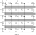
- FIG. 15 is a schematic illustration of routing between the row drivers 66 and the column drivers 68 of the backlight 13 , which includes 5 rows and 40 columns.
- each tile may include a set of backlight elements 122 , a row driver 66 , and a column driver 68 , where the row driver 66 and the column driver 68 drive the set of backlight elements.
- the row driver 66 may be coupled to multiple signal lines or traces (e.g., 3, 5, 7 signal lines), and the column driver 68 may also be coupled to multiple signal lines.
- the row driver 66 and the column driver 68 may be connected to each other via respective signal lines.
- the connection 140 between the row driver 66 and the column driver 68 may include a via (e.g., top and bottom layered connection).
- FIG. 16 A is a schematic illustration of a top view of the backlight 13 that includes the printed circuit board 130 and an interposer board 132 .
- the printed circuit board 130 may include the backlight elements 122 while the interposer board 132 includes the driver circuitry 70 (e.g., backlight controller (BCON) 62 and the row and column driver circuitry 70 ) and the off-board connector 64 .
- a first portion of the interposer board 132 may include a greater number of the driver circuitry 70 and/or the off-board connectors 64 compared to a second portion of the interposer board 132 .
- two portion of the interposer board 132 may include an equal number of the driver circuitry 70 and/or the off-board connectors 64 .
- FIG. 16 B is a schematic illustration of a side view of the backlight of FIG. 7 having the printed circuit board 130 and the interposer board 132 .
- the interposer board 132 is disposed on top of the printed circuit board 130 , and the interposer board 132 is smaller in area than the printed circuit board 130 by a threshold amount (e.g., the interposer board 132 is 10%, 20%, or 30% of the size of the printed circuit board 130 ).
- FIG. 17 is a schematic illustration of a top view of the backlight 13 associated with spine routing 125 , in which the off-board connector 64 and the row and column driver circuitry 70 are disposed along.
- This spine-based arrangement of the backlight 13 helps reduce the area of ground loop within the backlight. Reducing the ground loop reduces noise interference between components (e.g., board connector 64 , row and column driver circuitry 70 ) of the backlight 13 , and thereby improves signal and power integrity (SIPI).
- SIPI signal and power integrity
- the backlight of large sized displays may be divided into tiles such that each tile is driven by a respective driver circuitry.
- By driving a set of backlight elements within a tile via a respective driver circuitry reduces the total number of driver circuitry within the backlight, and thereby reduces the manufacturing cost of the backlight and the electronic display.
- components of the backlight such as the respective driver circuitry, backlight controller (BCON), and the off-board connector may be arranged in any suitable configuration (e.g., spine routing, rib-cage routing). Configurations that include spine routing and rib-cage routing may improve routing between backlight elements and provide signal and power integrity (SIPI) benefits.
- SIPI signal and power integrity
- personally identifiable information should follow privacy policies and practices that are generally recognized as meeting or exceeding industry or governmental requirements for maintaining the privacy of users.
- personally identifiable information data should be managed and handled so as to minimize risks of unintentional or unauthorized access or use, and the nature of authorized use should be clearly indicated to users.
Landscapes
- Engineering & Computer Science (AREA)
- Physics & Mathematics (AREA)
- Computer Hardware Design (AREA)
- General Physics & Mathematics (AREA)
- Theoretical Computer Science (AREA)
- Liquid Crystal Display Device Control (AREA)
Abstract
Description
Claims (18)
Priority Applications (1)
| Application Number | Priority Date | Filing Date | Title |
|---|---|---|---|
| US17/980,252 US12131712B2 (en) | 2021-12-10 | 2022-11-03 | Tile passive matrix for display backlight systems |
Applications Claiming Priority (2)
| Application Number | Priority Date | Filing Date | Title |
|---|---|---|---|
| US202163288309P | 2021-12-10 | 2021-12-10 | |
| US17/980,252 US12131712B2 (en) | 2021-12-10 | 2022-11-03 | Tile passive matrix for display backlight systems |
Publications (2)
| Publication Number | Publication Date |
|---|---|
| US20230186865A1 US20230186865A1 (en) | 2023-06-15 |
| US12131712B2 true US12131712B2 (en) | 2024-10-29 |
Family
ID=86694796
Family Applications (1)
| Application Number | Title | Priority Date | Filing Date |
|---|---|---|---|
| US17/980,252 Active US12131712B2 (en) | 2021-12-10 | 2022-11-03 | Tile passive matrix for display backlight systems |
Country Status (1)
| Country | Link |
|---|---|
| US (1) | US12131712B2 (en) |
Citations (11)
| Publication number | Priority date | Publication date | Assignee | Title |
|---|---|---|---|---|
| US20070284994A1 (en) * | 2006-05-29 | 2007-12-13 | Sharp Kabushiki Kaisha | Light emitting apparatus, display apparatus and method for controlling light emitting apparatus |
| US20080245949A1 (en) * | 2005-10-07 | 2008-10-09 | Sharp Kabushiki Kaisha | Backlight device, display apparatus including backlight device, method for driving backlight device, and method for adjusting backlight device |
| US20130016306A1 (en) * | 2011-07-15 | 2013-01-17 | Canon Kabushiki Kaisha | Backlight apparatus, method for controlling the same, and image display apparatus |
| US20130147782A1 (en) * | 2011-12-09 | 2013-06-13 | Au Optronics Corp. | Data driving apparatus and operation method thereof and display using the same |
| US20170047393A1 (en) * | 2014-09-25 | 2017-02-16 | X-Celeprint Limited | Display tile structure and tiled display |
| US20170316758A1 (en) | 2008-06-25 | 2017-11-02 | Dolby Laboratories Licensing Corporation | High Dynamic Range Display Using LED Backlighting, Stacked Optical Films, and LCD Drive Signals Based on a Low Resolution Light Field Simulation |
| US10665181B2 (en) | 2017-06-28 | 2020-05-26 | Apple Inc. | Backlights with dynamic dimming ranges |
| US20200319512A1 (en) * | 2019-04-02 | 2020-10-08 | Visteon Global Technologies, Inc. | Display system |
| US20210097943A1 (en) | 2019-04-11 | 2021-04-01 | PixeIDisplay Inc. | Method and apparatus of a multi-modal illumination and display for improved color rendering, power efficiency, health and eye-safety |
| US20210116749A1 (en) * | 2019-10-18 | 2021-04-22 | Innolux Corporation | Display device |
| US11081070B2 (en) | 2018-09-18 | 2021-08-03 | Apple Inc. | Backlight systems and methods for electronic device displays |
-
2022
- 2022-11-03 US US17/980,252 patent/US12131712B2/en active Active
Patent Citations (11)
| Publication number | Priority date | Publication date | Assignee | Title |
|---|---|---|---|---|
| US20080245949A1 (en) * | 2005-10-07 | 2008-10-09 | Sharp Kabushiki Kaisha | Backlight device, display apparatus including backlight device, method for driving backlight device, and method for adjusting backlight device |
| US20070284994A1 (en) * | 2006-05-29 | 2007-12-13 | Sharp Kabushiki Kaisha | Light emitting apparatus, display apparatus and method for controlling light emitting apparatus |
| US20170316758A1 (en) | 2008-06-25 | 2017-11-02 | Dolby Laboratories Licensing Corporation | High Dynamic Range Display Using LED Backlighting, Stacked Optical Films, and LCD Drive Signals Based on a Low Resolution Light Field Simulation |
| US20130016306A1 (en) * | 2011-07-15 | 2013-01-17 | Canon Kabushiki Kaisha | Backlight apparatus, method for controlling the same, and image display apparatus |
| US20130147782A1 (en) * | 2011-12-09 | 2013-06-13 | Au Optronics Corp. | Data driving apparatus and operation method thereof and display using the same |
| US20170047393A1 (en) * | 2014-09-25 | 2017-02-16 | X-Celeprint Limited | Display tile structure and tiled display |
| US10665181B2 (en) | 2017-06-28 | 2020-05-26 | Apple Inc. | Backlights with dynamic dimming ranges |
| US11081070B2 (en) | 2018-09-18 | 2021-08-03 | Apple Inc. | Backlight systems and methods for electronic device displays |
| US20200319512A1 (en) * | 2019-04-02 | 2020-10-08 | Visteon Global Technologies, Inc. | Display system |
| US20210097943A1 (en) | 2019-04-11 | 2021-04-01 | PixeIDisplay Inc. | Method and apparatus of a multi-modal illumination and display for improved color rendering, power efficiency, health and eye-safety |
| US20210116749A1 (en) * | 2019-10-18 | 2021-04-22 | Innolux Corporation | Display device |
Also Published As
| Publication number | Publication date |
|---|---|
| US20230186865A1 (en) | 2023-06-15 |
Similar Documents
| Publication | Publication Date | Title |
|---|---|---|
| US10657912B2 (en) | Display with pixel dimming for curved edges | |
| AU2012315618B2 (en) | Optical system and method to mimic zero-border display | |
| KR20220160697A (en) | Display with Viewer Tracking | |
| KR102692389B1 (en) | Touch display device and display panel | |
| US10043472B2 (en) | Digital compensation for V-gate coupling | |
| KR20210099972A (en) | Operating Method for Gamma Voltage corresponding to display area and electronic device supporting the same | |
| US10777113B2 (en) | Display device | |
| CN113140152B (en) | Display panel and terminal equipment | |
| US10170072B2 (en) | Gate line layout configuration | |
| US20210074207A1 (en) | Gradual change of pixel-resolution in oled display | |
| US20220375427A1 (en) | Systems and Methods for Tile Boundary Compensation | |
| US12131712B2 (en) | Tile passive matrix for display backlight systems | |
| US20170061837A1 (en) | V-gate layout and gate drive configuration | |
| US12300161B2 (en) | Optical crosstalk compensation for foveated display | |
| US20240029625A1 (en) | Multiple-row display driving to mitigate touch sensor subsystem interaction | |
| US12062313B2 (en) | Systems and methods for clock frequency control during low display refresh rates in electronic devices | |
| US12380835B2 (en) | Electronic display pixel grouping to mitigate motion blur | |
| US12189901B2 (en) | Split display driver circuitry to mitigate touch sensing system interaction | |
| US12322314B2 (en) | Display and antenna co-design to reduce antenna transmission loss | |
| US12424139B2 (en) | Pulse splitting for motion artifact reduction | |
| US20250292718A1 (en) | Systems and Methods for Compensating for Scan Signal Induced Odd-Even Row Mismatch | |
| US12205510B2 (en) | Spatiotemporal dither for pulsed digital display systems and methods | |
| WO2024019948A1 (en) | Multiple-row display driving to mitigate touch sensor subsystem interaction | |
| US20250299624A1 (en) | Electronic Display Self-Coupling Cross Talk Compensation | |
| US11227558B1 (en) | Subpixel layout compensation to correct color fringing on an electronic display |
Legal Events
| Date | Code | Title | Description |
|---|---|---|---|
| FEPP | Fee payment procedure |
Free format text: ENTITY STATUS SET TO UNDISCOUNTED (ORIGINAL EVENT CODE: BIG.); ENTITY STATUS OF PATENT OWNER: LARGE ENTITY |
|
| AS | Assignment |
Owner name: APPLE INC., CALIFORNIA Free format text: ASSIGNMENT OF ASSIGNORS INTEREST;ASSIGNORS:CALAYIR, VEHBI;JEONG, YOUCHUL;GOLDMAN, JOSHUA D.;SIGNING DATES FROM 20221028 TO 20221107;REEL/FRAME:061768/0734 |
|
| STPP | Information on status: patent application and granting procedure in general |
Free format text: NON FINAL ACTION MAILED |
|
| STPP | Information on status: patent application and granting procedure in general |
Free format text: RESPONSE TO NON-FINAL OFFICE ACTION ENTERED AND FORWARDED TO EXAMINER |
|
| STPP | Information on status: patent application and granting procedure in general |
Free format text: FINAL REJECTION MAILED |
|
| STPP | Information on status: patent application and granting procedure in general |
Free format text: RESPONSE AFTER FINAL ACTION FORWARDED TO EXAMINER |
|
| STPP | Information on status: patent application and granting procedure in general |
Free format text: ADVISORY ACTION MAILED |
|
| STPP | Information on status: patent application and granting procedure in general |
Free format text: DOCKETED NEW CASE - READY FOR EXAMINATION |
|
| STPP | Information on status: patent application and granting procedure in general |
Free format text: NON FINAL ACTION MAILED |
|
| STPP | Information on status: patent application and granting procedure in general |
Free format text: RESPONSE TO NON-FINAL OFFICE ACTION ENTERED AND FORWARDED TO EXAMINER |
|
| STPP | Information on status: patent application and granting procedure in general |
Free format text: NOTICE OF ALLOWANCE MAILED -- APPLICATION RECEIVED IN OFFICE OF PUBLICATIONS |
|
| STPP | Information on status: patent application and granting procedure in general |
Free format text: PUBLICATIONS -- ISSUE FEE PAYMENT RECEIVED |
|
| STCF | Information on status: patent grant |
Free format text: PATENTED CASE |