US12119236B2 - Method for producing a connection structure and semiconductor device - Google Patents
Method for producing a connection structure and semiconductor device Download PDFInfo
- Publication number
- US12119236B2 US12119236B2 US17/442,624 US202017442624A US12119236B2 US 12119236 B2 US12119236 B2 US 12119236B2 US 202017442624 A US202017442624 A US 202017442624A US 12119236 B2 US12119236 B2 US 12119236B2
- Authority
- US
- United States
- Prior art keywords
- substrate
- main surface
- carrier substrate
- layer
- opening
- Prior art date
- Legal status (The legal status is an assumption and is not a legal conclusion. Google has not performed a legal analysis and makes no representation as to the accuracy of the status listed.)
- Active, expires
Links
Images


Classifications
-
- H—ELECTRICITY
- H10—SEMICONDUCTOR DEVICES; ELECTRIC SOLID-STATE DEVICES NOT OTHERWISE PROVIDED FOR
- H10W—GENERIC PACKAGES, INTERCONNECTIONS, CONNECTORS OR OTHER CONSTRUCTIONAL DETAILS OF DEVICES COVERED BY CLASS H10
- H10W20/00—Interconnections in chips, wafers or substrates
- H10W20/01—Manufacture or treatment
- H10W20/021—Manufacture or treatment of interconnections within wafers or substrates
- H10W20/023—Manufacture or treatment of interconnections within wafers or substrates the interconnections being through-semiconductor vias
-
- H—ELECTRICITY
- H10—SEMICONDUCTOR DEVICES; ELECTRIC SOLID-STATE DEVICES NOT OTHERWISE PROVIDED FOR
- H10W—GENERIC PACKAGES, INTERCONNECTIONS, CONNECTORS OR OTHER CONSTRUCTIONAL DETAILS OF DEVICES COVERED BY CLASS H10
- H10W70/00—Package substrates; Interposers; Redistribution layers [RDL]
- H10W70/01—Manufacture or treatment
- H10W70/05—Manufacture or treatment of insulating or insulated package substrates, or of interposers, or of redistribution layers
- H10W70/095—Manufacture or treatment of insulating or insulated package substrates, or of interposers, or of redistribution layers of vias therein
-
- H01L21/486—
-
- H01L21/76871—
-
- H01L23/5384—
-
- H01L23/5386—
-
- H—ELECTRICITY
- H10—SEMICONDUCTOR DEVICES; ELECTRIC SOLID-STATE DEVICES NOT OTHERWISE PROVIDED FOR
- H10W—GENERIC PACKAGES, INTERCONNECTIONS, CONNECTORS OR OTHER CONSTRUCTIONAL DETAILS OF DEVICES COVERED BY CLASS H10
- H10W20/00—Interconnections in chips, wafers or substrates
- H10W20/01—Manufacture or treatment
- H10W20/021—Manufacture or treatment of interconnections within wafers or substrates
- H10W20/023—Manufacture or treatment of interconnections within wafers or substrates the interconnections being through-semiconductor vias
- H10W20/0245—Manufacture or treatment of interconnections within wafers or substrates the interconnections being through-semiconductor vias comprising use of blind vias during the manufacture
-
- H—ELECTRICITY
- H10—SEMICONDUCTOR DEVICES; ELECTRIC SOLID-STATE DEVICES NOT OTHERWISE PROVIDED FOR
- H10W—GENERIC PACKAGES, INTERCONNECTIONS, CONNECTORS OR OTHER CONSTRUCTIONAL DETAILS OF DEVICES COVERED BY CLASS H10
- H10W20/00—Interconnections in chips, wafers or substrates
- H10W20/01—Manufacture or treatment
- H10W20/021—Manufacture or treatment of interconnections within wafers or substrates
- H10W20/023—Manufacture or treatment of interconnections within wafers or substrates the interconnections being through-semiconductor vias
- H10W20/0261—Manufacture or treatment of interconnections within wafers or substrates the interconnections being through-semiconductor vias characterised by the filling method or the material of the conductive fill
-
- H—ELECTRICITY
- H10—SEMICONDUCTOR DEVICES; ELECTRIC SOLID-STATE DEVICES NOT OTHERWISE PROVIDED FOR
- H10W—GENERIC PACKAGES, INTERCONNECTIONS, CONNECTORS OR OTHER CONSTRUCTIONAL DETAILS OF DEVICES COVERED BY CLASS H10
- H10W20/00—Interconnections in chips, wafers or substrates
- H10W20/01—Manufacture or treatment
- H10W20/021—Manufacture or treatment of interconnections within wafers or substrates
- H10W20/023—Manufacture or treatment of interconnections within wafers or substrates the interconnections being through-semiconductor vias
- H10W20/0265—Manufacture or treatment of interconnections within wafers or substrates the interconnections being through-semiconductor vias characterised by the sidewall insulation
-
- H—ELECTRICITY
- H10—SEMICONDUCTOR DEVICES; ELECTRIC SOLID-STATE DEVICES NOT OTHERWISE PROVIDED FOR
- H10W—GENERIC PACKAGES, INTERCONNECTIONS, CONNECTORS OR OTHER CONSTRUCTIONAL DETAILS OF DEVICES COVERED BY CLASS H10
- H10W20/00—Interconnections in chips, wafers or substrates
- H10W20/01—Manufacture or treatment
- H10W20/031—Manufacture or treatment of conductive parts of the interconnections
- H10W20/032—Manufacture or treatment of conductive parts of the interconnections of conductive barrier, adhesion or liner layers
- H10W20/042—Manufacture or treatment of conductive parts of the interconnections of conductive barrier, adhesion or liner layers the barrier, adhesion or liner layers being seed or nucleation layers
-
- H—ELECTRICITY
- H10—SEMICONDUCTOR DEVICES; ELECTRIC SOLID-STATE DEVICES NOT OTHERWISE PROVIDED FOR
- H10W—GENERIC PACKAGES, INTERCONNECTIONS, CONNECTORS OR OTHER CONSTRUCTIONAL DETAILS OF DEVICES COVERED BY CLASS H10
- H10W70/00—Package substrates; Interposers; Redistribution layers [RDL]
- H10W70/60—Insulating or insulated package substrates; Interposers; Redistribution layers
- H10W70/611—Insulating or insulated package substrates; Interposers; Redistribution layers for connecting multiple chips together
-
- H—ELECTRICITY
- H10—SEMICONDUCTOR DEVICES; ELECTRIC SOLID-STATE DEVICES NOT OTHERWISE PROVIDED FOR
- H10W—GENERIC PACKAGES, INTERCONNECTIONS, CONNECTORS OR OTHER CONSTRUCTIONAL DETAILS OF DEVICES COVERED BY CLASS H10
- H10W70/00—Package substrates; Interposers; Redistribution layers [RDL]
- H10W70/60—Insulating or insulated package substrates; Interposers; Redistribution layers
- H10W70/62—Insulating or insulated package substrates; Interposers; Redistribution layers characterised by their interconnections
- H10W70/63—Vias, e.g. via plugs
- H10W70/635—Through-vias
-
- H—ELECTRICITY
- H10—SEMICONDUCTOR DEVICES; ELECTRIC SOLID-STATE DEVICES NOT OTHERWISE PROVIDED FOR
- H10W—GENERIC PACKAGES, INTERCONNECTIONS, CONNECTORS OR OTHER CONSTRUCTIONAL DETAILS OF DEVICES COVERED BY CLASS H10
- H10W70/00—Package substrates; Interposers; Redistribution layers [RDL]
- H10W70/60—Insulating or insulated package substrates; Interposers; Redistribution layers
- H10W70/62—Insulating or insulated package substrates; Interposers; Redistribution layers characterised by their interconnections
- H10W70/65—Shapes or dispositions of interconnections
-
- H—ELECTRICITY
- H10—SEMICONDUCTOR DEVICES; ELECTRIC SOLID-STATE DEVICES NOT OTHERWISE PROVIDED FOR
- H10P—GENERIC PROCESSES OR APPARATUS FOR THE MANUFACTURE OR TREATMENT OF DEVICES COVERED BY CLASS H10
- H10P14/00—Formation of materials, e.g. in the shape of layers or pillars
- H10P14/40—Formation of materials, e.g. in the shape of layers or pillars of conductive or resistive materials
- H10P14/46—Formation of materials, e.g. in the shape of layers or pillars of conductive or resistive materials using a liquid
- H10P14/47—Electrolytic deposition, i.e. electroplating; Electroless plating
Definitions
- the present disclosure relates to a connection structure and a semiconductor device.
- Semiconductor devices are widely used in a wide variety of fields of application. Semiconductor devices are, for example, manufactured by processing semiconductor wafers, which are separated into individual semiconductor chips after processing steps have been carried out at the wafer level. For electrical contacting, individual semiconductor chips or processed semiconductor wafers may be joined together with and electrically connected to a substrate in which a plurality of connection structures are formed.
- the present disclosure is based on the object of providing an improved method of manufacturing a connection structure and an improved semiconductor device.
- a method of manufacturing a connection structure comprises forming an opening in a first main surface of a first substrate, forming a galvanic seed layer over a first main surface of a carrier substrate, and connecting the first main surface of the first substrate to the first main surface of the carrier substrate, so that the galvanic seed layer is arranged between the first main surface of the first substrate and the first main surface of the carrier substrate.
- the method further includes galvanically forming a conductive material over the galvanic seed layer.
- the method further includes thinning the first substrate so that the opening in the first substrate is opened on a second main surface of the first substrate facing away from the carrier substrate.
- the method may include forming an insulation layer over sidewalls of the opening in the first substrate.
- connecting the first main surface of the first substrate to the first main surface of the carrier substrate may include applying a connection layer between the galvanic seed layer and the first main surface of the first substrate. Furthermore, the method may include removing the connection layer from the surface of the openings facing the carrier substrate after the first substrate and the carrier substrate have been joined together, so that the galvanic seed layer becomes exposed. According to embodiments, the conductive material may completely fill the opening in the first substrate.
- the opening in the first substrate may have a width greater than 20 ⁇ m.
- a depth of the opening in the first substrate may, for example, be greater than 50 ⁇ m.
- the method may further include forming a separating layer over the carrier substrate, with the separating layer being arranged between the galvanic seed layer and the first main surface of the carrier substrate.
- the method may further include connecting the second main surface of the first substrate to a second semiconductor substrate within which a functional portion is arranged, so that the functional portion is electrically connected to the conductive material.
- the method may further comprise removing the carrier substrate after the main surface of the first substrate facing away from the carrier substrate has been connected to the functional portion.
- a semiconductor device is manufactured according to the method described above.
- a semiconductor device comprises a first semiconductor substrate having a first main surface, with the first main surface containing an opening, an insulation layer being arranged over sidewalls of the opening and the opening being filled with a conductive material. Furthermore, the semiconductor device includes a second semiconductor substrate within which a functional portion is arranged, which is electrically connected to the conductive material.
- the functional portion in the semiconductor device described above may be an optoelectronic semiconductor device.
- the conductive material in the semiconductor device described above may be nickel or aluminum.
- the opening may, in the semiconductor device described above, have a depth greater than 50 ⁇ m.
- FIGS. 1 to 4 each show vertical cross-sectional views of a workpiece whilst carrying out the method of manufacturing a connection structure according to embodiments.
- FIG. 5 shows a vertical cross-sectional view of a semiconductor device.
- FIG. 6 summarizes a method according to embodiments.
- substrate used within the scope of the present description generally includes insulating, conductive or semiconductor substrates.
- vertical is intended to describe an orientation which is essentially perpendicular to the first surface of a substrate or semiconductor body.
- the vertical direction may, for example, correspond to a direction of growth when layers are grown on.
- lateral and horizontal are intended to describe an orientation or alignment which runs essentially parallel to a first surface of a substrate or semiconductor body. This may, for example, be the surface of a wafer or a chip (die).
- the horizontal direction may, for example, lie in a plane perpendicular to a direction of growth when layers are grown on.
- electrically connected means a low-ohmic electrical connection between the connected elements.
- the electrically connected elements need not necessarily be directly connected to one another.
- Additional elements may be arranged between electrically connected elements.
- electrically connected also includes tunnel contact between the connected elements.
- FIG. 1 shows a vertical cross-sectional view of a workpiece whilst carrying out the method of manufacturing a connection structure according to embodiments.
- a vertical cross-sectional view through a first substrate 100 can be seen.
- the first substrate 100 may, for example, be a semiconductor substrate, e.g. a silicon substrate.
- the first substrate 100 contains a plurality of openings 15 .
- the openings 15 are formed in the first main surface 101 of the first substrate 100 .
- the openings 15 may extend in the vertical direction through the first substrate.
- the openings 15 may be formed by means of ion etching using a photolithographic mask.
- the openings 15 may, for example, have a width greater than 20 ⁇ m. Furthermore, the openings 15 may, for example, have a width of less than 50 ⁇ m. In this process, “width” denotes a maximum dimension in a lateral direction.
- the depth of the openings 15 may be greater than 50 ⁇ m. Furthermore, the depth of the openings 15 may be more than 100 ⁇ m. For example, the depth of the openings may be up to approximately 200 ⁇ m, for example, approximately 150 ⁇ m. In this process, “depth” denotes a maximum dimension in a vertical direction.
- the openings 15 may, for example, be cylindrical.
- the cylinder axis may run in a vertical direction.
- the lateral cross-sectional area of the cylinder may, for example, have a circular, elliptical, rectangular or any other form.
- the openings 15 may be designed as so-called blind holes, so that, starting from the first main surface 101 of the first substrate 100 , they extend in the vertical direction through the first substrate 100 and, in this process, do not completely penetrate the first substrate 100 .
- the first substrate 100 is connected to a carrier substrate 110 .
- a first connection layer 130 a is applied on the first main surface 101 of the first substrate 100 .
- the first connection layer 130 a may, for example, be a silicon oxide layer.
- connection layer refers to a physical connection of elements.
- the first connection layer 130 a may, in particular, be insulating.
- the first connection layer 130 a may also be applied on the sidewalls 20 of the openings 15 , so that the first connection layer 130 a there becomes part of an insulation layer 155 covering the sidewalls 20 .
- the insulation layer 155 may be vapor-deposited, for example, by a CVD (chemical vapor deposition) process.
- the insulation layer may also be sputtered on. In this way—for example, in comparison to a thermal oxidation process—an insulation layer having the necessary thickness and quality may be produced in order to provide effective electrical insulation.
- the first connection layer 130 a and the insulation layer 155 may also be produced by separate processes.
- the insulation layer 155 may be applied by a CVD or sputtering process, as stated above, as a result of which good insulation of the sidewalls 20 of the openings is ensured.
- the connection layer 130 a may be produced as spin-on-glass, that is to say, for example, by spin-coating.
- a galvanic seed layer 120 is formed over a first main surface 111 of the carrier substrate 110 .
- the carrier substrate 110 may, for example, be a semiconductor substrate, e.g. a silicon or a sapphire substrate.
- the galvanic seed layer 120 may, for example, be a gold layer.
- a separating layer 140 may further be formed over the first main surface 111 of the carrier substrate 110 .
- the separating layer 140 may, for example, contain silicon nitride.
- the separating layer 140 may be arranged between the galvanic seed layer 120 and the first main surface 111 of the carrier substrate 110 .
- the method may further include forming a second connection layer 130 b over the galvanic seed layer 120 .
- the first main surface 101 of the first substrate 100 and the first main surface 111 of the carrier substrate 110 are connected to one another in such a manner that the galvanic seed layer 120 is arranged between the first main surface 101 of the first substrate 100 and the first main surface 111 of the carrier substrate 110 .
- the workpiece shown in FIG. 2 may be obtained.
- first connection layer 130 a and the second connection layer 130 b may come into contact with one another and form a connected connection layer 130 .
- the first substrate 100 may be thinned on a side facing away from the carrier substrate 110 .
- the thinning of the first substrate 100 may, for example, include a grinding back process and, if necessary, also a chemical mechanical polishing process (CMP).
- CMP chemical mechanical polishing process
- the openings 15 may be exposed on a second main surface 102 of the first substrate 100 facing away from the carrier substrate 110 . If necessary, the connection layer 130 may then be removed from the surface of the openings 15 facing the carrier substrate 110 and from the sidewalls 20 of the openings 15 .
- a passivation layer 150 may subsequently be applied on the second main surface 102 of the first substrate 100 .
- the passivation layer 150 may contain silicon oxide or silicon nitride.
- the passivation layer 150 may also be applied on the sidewalls 20 of the openings 15 , so that the passivation layer 150 there becomes part of an insulation layer 155 covering the sidewalls 20 .
- connection layer 130 and the passivation layer 150 may be removed from the surface of the openings 15 facing the carrier substrate 110 .
- the galvanic seed layer 121 on the substantially horizontal boundary surface of the openings 15 facing the carrier substrate 110 is free of passivation or connection layers.
- the workpiece shown in FIG. 3 may be obtained.
- a galvanic process will be carried out.
- the workpiece may be placed in an electrolytic bath.
- a circuit may be established between a first pole and a second pole of a power source.
- the first pole of the power source may be electrically connected to a conductive material 160 located in the electrolytic bath.
- the second pole of the power source may be electrically connected to the galvanic seed layer 120 .
- the conductive material 160 may be deposited over the exposed part 121 of the galvanic seed layer 120 .
- the conductive material 160 may be a metal, for example, copper, nickel, or aluminum.
- the conductive material 160 may, for example, completely fill the openings 15 in the first substrate 100 .
- the workpiece shown in FIG. 4 may be obtained.
- the openings 15 are evenly filled from their surface facing the carrier substrate 110 in the galvanic process.
- the openings 15 on their side facing away from the carrier substrate 110 via which the conductive material 160 penetrates into the openings, are closed with the conductive material 160 before they have been completely filled with the conductive material 160 . Accordingly, the openings 15 may be uniformly filled without adding additional chemicals such as suppressors and/or accelerators and without voids.
- conductive materials such as nickel or aluminum may be deposited. In particular, conductive materials may be deposited for which such suppressors or accelerators are not known or not available.
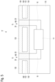
- a functional portion 14 may subsequently be electrically connected to the conductive material 160 , as illustrated in FIG. 5 .
- the second main surface 102 of the first substrate 100 may be connected to a second semiconductor substrate 170 .
- One or more functional portions 14 may be arranged within the second semiconductor substrate 170 .
- the functional portion 14 may be electrically connected to the conductive material 160 via one or more connection elements 16 .
- the functional portion 14 may, for example, be an optoelectronic component.
- the functional portion 14 may contain a first semiconductor layer of a first conductivity type, a second semiconductor layer of a second conductivity type, and an active region which is arranged between the first and second semiconductor layers.
- the functional portion 14 may also be designed in a different manner.
- a plurality of functional portions 14 may be arranged within the second semiconductor substrate 170 , each of which is connected to the conductive material 160 in an associated opening 15 .
- the carrier substrate 110 is removed in a subsequent process step.
- the carrier substrate 110 may be removed by means of a laser lift-off process.
- the carrier substrate 110 may be exposed to laser radiation.
- the laser radiation may be pulsed.
- a boundary layer between the carrier substrate 110 and the separating layer 140 may heat up in the process. As a result, the carrier substrate 110 may be detached from the separating layer 140 .
- the separating layer 140 may be removed. This may, for example, be done by chemical mechanical polishing.
- galvanic seed layer 120 may, for example, be removed by etching.
- the semiconductor device shown in FIG. 5 may be obtained.
- Functional portions 14 are arranged within the first semiconductor substrate 170 .
- the optoelectronic semiconductor portions are, for example, electrically connected to electrically conductive material 160 via connection elements 16 .
- the electrically conductive material 160 is arranged within openings 15 in a first substrate.
- the openings 15 extend from a first main surface 101 to a second main surface 102 of the first substrate 100 .
- the sidewalls 20 of the openings 15 are covered with a passivation layer 150 .
- the electrically conductive material may, for example, be nickel or aluminum. According to further embodiments, the electrically conductive material may also be copper.
- FIG. 6 summarizes a method of manufacturing a connection structure according to embodiments.
- the method includes forming (S 100 ) an opening in a first main surface of a first substrate, forming (S 200 ) a galvanic seed layer over a first main surface of a carrier substrate, and connecting (S 300 ) the first main surface of the first substrate to the first main surface of the carrier substrate, so that the galvanic seed layer is arranged between the first main surface of the first substrate and the first main surface of the carrier substrate.
- the method further includes galvanically forming (S 400 ) a conductive material over the galvanic seed layer.
Landscapes
- Internal Circuitry In Semiconductor Integrated Circuit Devices (AREA)
- Physics & Mathematics (AREA)
- Geometry (AREA)
- Electrodes Of Semiconductors (AREA)
Abstract
Description
- 12 semiconductor device
- 14 functional portion
- 15 opening
- 16 connection elements
- 20 sidewalls of the opening
- 100 first substrate
- 101 first main surface of the first substrate
- 102 second main surface of the first substrate
- 110 carrier substrate
- 111 first main surface of the carrier substrate
- 115 second substrate
- 120 galvanic seed layer
- 121 exposed part of the galvanic seed layer
- 130 a first connection layer
- 130 b second connection layer
- 130 merged connection layer
- 140 separating layer
- 150 passivation layer
- 155 insulation layer
- 160 conductive material
- 170 second semiconductor substrate
Claims (10)
Applications Claiming Priority (3)
| Application Number | Priority Date | Filing Date | Title |
|---|---|---|---|
| DE102019107760.5 | 2019-03-26 | ||
| DE102019107760.5A DE102019107760A1 (en) | 2019-03-26 | 2019-03-26 | METHOD FOR PRODUCING A CONNECTING STRUCTURE AND SEMICONDUCTOR COMPONENT |
| PCT/EP2020/057784 WO2020193408A1 (en) | 2019-03-26 | 2020-03-20 | Method for producing a connnection structure and semiconductor component |
Publications (2)
| Publication Number | Publication Date |
|---|---|
| US20220172960A1 US20220172960A1 (en) | 2022-06-02 |
| US12119236B2 true US12119236B2 (en) | 2024-10-15 |
Family
ID=69960631
Family Applications (1)
| Application Number | Title | Priority Date | Filing Date |
|---|---|---|---|
| US17/442,624 Active 2041-01-20 US12119236B2 (en) | 2019-03-26 | 2020-03-20 | Method for producing a connection structure and semiconductor device |
Country Status (3)
| Country | Link |
|---|---|
| US (1) | US12119236B2 (en) |
| DE (2) | DE102019107760A1 (en) |
| WO (1) | WO2020193408A1 (en) |
Citations (11)
| Publication number | Priority date | Publication date | Assignee | Title |
|---|---|---|---|---|
| US20060046432A1 (en) * | 2004-08-25 | 2006-03-02 | Agency For Science, Technology And Research | Method of forming through-wafer interconnects for vertical wafer level packaging |
| EP1749794A2 (en) | 2005-08-01 | 2007-02-07 | Shinko Electric Industries Co., Ltd. | Electronic parts packaging structure and method of manufacturing the same |
| US20070180916A1 (en) | 2006-02-09 | 2007-08-09 | General Electric Company | Capacitive micromachined ultrasound transducer and methods of making the same |
| US20080164573A1 (en) * | 2007-01-05 | 2008-07-10 | Basker Veeraraghaven S | Methods for fabricating silicon carriers with conductive through-vias with low stress and low defect density |
| US20080315230A1 (en) | 2007-06-20 | 2008-12-25 | Shinko Electric Industries Co., Ltd. | Electronic component package and method of manufacturing the same, and electronic component device |
| US20090255716A1 (en) | 2006-05-02 | 2009-10-15 | Ibiden Co., Ltd. | Heat resistant substrate incorporated circuit wiring board |
| US20110111560A1 (en) * | 2008-09-26 | 2011-05-12 | International Business Machines Corporation | Lock and Key Through-Via Method for Wafer Level 3D Integration and Structures Produced Thereby |
| WO2012119333A1 (en) * | 2011-03-04 | 2012-09-13 | 中国科学院微电子研究所 | Through-silicon-via (tsv) structure and its fabricating method |
| CN103700595A (en) * | 2013-12-17 | 2014-04-02 | 中国电子科技集团公司第五十八研究所 | Wafer level high-aspect-ratio TSV (through silicon via) package substrate preparation method |
| US20160276174A1 (en) * | 2015-03-18 | 2016-09-22 | Amkor Technology, Inc. | Semiconductor device and manufacturing method thereof |
| US20180151475A1 (en) | 2016-11-29 | 2018-05-31 | Canon Kabushiki Kaisha | Semiconductor device and manufacturing method thereof |
-
2019
- 2019-03-26 DE DE102019107760.5A patent/DE102019107760A1/en not_active Withdrawn
-
2020
- 2020-03-20 US US17/442,624 patent/US12119236B2/en active Active
- 2020-03-20 DE DE112020001468.1T patent/DE112020001468A5/en active Pending
- 2020-03-20 WO PCT/EP2020/057784 patent/WO2020193408A1/en not_active Ceased
Patent Citations (13)
| Publication number | Priority date | Publication date | Assignee | Title |
|---|---|---|---|---|
| US20060046432A1 (en) * | 2004-08-25 | 2006-03-02 | Agency For Science, Technology And Research | Method of forming through-wafer interconnects for vertical wafer level packaging |
| EP1749794A2 (en) | 2005-08-01 | 2007-02-07 | Shinko Electric Industries Co., Ltd. | Electronic parts packaging structure and method of manufacturing the same |
| US20070180916A1 (en) | 2006-02-09 | 2007-08-09 | General Electric Company | Capacitive micromachined ultrasound transducer and methods of making the same |
| DE102007007178A1 (en) | 2006-02-09 | 2007-08-30 | General Electric Co. | Capacitive micromachined ultrasonic transducers and methods of making the same |
| US20090255716A1 (en) | 2006-05-02 | 2009-10-15 | Ibiden Co., Ltd. | Heat resistant substrate incorporated circuit wiring board |
| US20080164573A1 (en) * | 2007-01-05 | 2008-07-10 | Basker Veeraraghaven S | Methods for fabricating silicon carriers with conductive through-vias with low stress and low defect density |
| US20080315230A1 (en) | 2007-06-20 | 2008-12-25 | Shinko Electric Industries Co., Ltd. | Electronic component package and method of manufacturing the same, and electronic component device |
| US20110111560A1 (en) * | 2008-09-26 | 2011-05-12 | International Business Machines Corporation | Lock and Key Through-Via Method for Wafer Level 3D Integration and Structures Produced Thereby |
| WO2012119333A1 (en) * | 2011-03-04 | 2012-09-13 | 中国科学院微电子研究所 | Through-silicon-via (tsv) structure and its fabricating method |
| CN103700595A (en) * | 2013-12-17 | 2014-04-02 | 中国电子科技集团公司第五十八研究所 | Wafer level high-aspect-ratio TSV (through silicon via) package substrate preparation method |
| CN103700595B (en) * | 2013-12-17 | 2016-07-06 | 中国电子科技集团公司第五十八研究所 | A kind of wafer scale high-aspect-ratio TSV base plate for packaging preparation method |
| US20160276174A1 (en) * | 2015-03-18 | 2016-09-22 | Amkor Technology, Inc. | Semiconductor device and manufacturing method thereof |
| US20180151475A1 (en) | 2016-11-29 | 2018-05-31 | Canon Kabushiki Kaisha | Semiconductor device and manufacturing method thereof |
Non-Patent Citations (2)
| Title |
|---|
| International Search Report for the corresponding PCT application No. PCT/EP2020/057784, mailed Jun. 9, 2020, 4p.p (for informational purposes only). |
| Search Report for the corresponding German Patent application No. 10 2019 107 760.5, issued Oct. 21, 2019, 7 p.p. (for informational purposes, only). |
Also Published As
| Publication number | Publication date |
|---|---|
| US20220172960A1 (en) | 2022-06-02 |
| WO2020193408A1 (en) | 2020-10-01 |
| DE102019107760A1 (en) | 2020-10-01 |
| DE112020001468A5 (en) | 2021-12-09 |
Similar Documents
| Publication | Publication Date | Title |
|---|---|---|
| KR101988893B1 (en) | Semiconductor device and a method of manufacturing the same | |
| US10748787B2 (en) | Semiconductor device with plated lead frame | |
| US10720495B2 (en) | Semiconductor device and manufacturing method thereof | |
| US10236419B2 (en) | Component and metod for producing a component | |
| US20120012994A1 (en) | Method for manufacturing semiconductor devices having a glass substrate | |
| US7795137B2 (en) | Manufacturing method of semiconductor device | |
| US20020048889A1 (en) | Method of manufacturing semiconductor device with sidewall metal layers | |
| US20170372952A1 (en) | Substrate and method including forming a via comprising a conductive liner layer and conductive plug having different microstructures | |
| US11823891B2 (en) | Backside metallized compound semiconductor device and method for manufacturing the same | |
| KR101841631B1 (en) | High electron mobility transistor and fabrication method thereof | |
| US12469817B2 (en) | Support structure to reinforce stacked semiconductor wafers | |
| US9847467B2 (en) | Optoelectronic component and method for the production thereof | |
| US20240170475A1 (en) | Method for manufacturing semiconductor device, semiconductor device, integrated circuit element, and method for manufacturing integrated circuit element | |
| US8896128B2 (en) | Integrated circuit, a semiconductor die arrangement and a method for manufacturing an integrated circuit | |
| US7948088B2 (en) | Semiconductor device | |
| US12341067B2 (en) | Manufacturing method of semiconductor device | |
| US12119236B2 (en) | Method for producing a connection structure and semiconductor device | |
| CN108511415B (en) | Method for manufacturing electronic assembly | |
| US20230097227A1 (en) | Semiconductor device and method of manufacturing the same | |
| US11437540B2 (en) | Component having metal carrier layer and layer that compensates for internal mechanical strains | |
| CN117476546A (en) | Methods of manufacturing semiconductor devices and corresponding semiconductor products | |
| US20260082840A1 (en) | Method for manufacturing semiconductor device, and semiconductor device | |
| CN114613684B (en) | Semiconductor packaging method | |
| TW202433701A (en) | Semiconductor device with stacked conductive layers and related methods | |
| US20100084768A1 (en) | Electronic component, a semiconductor wafer and a method for producing an electronic component |
Legal Events
| Date | Code | Title | Description |
|---|---|---|---|
| FEPP | Fee payment procedure |
Free format text: ENTITY STATUS SET TO UNDISCOUNTED (ORIGINAL EVENT CODE: BIG.); ENTITY STATUS OF PATENT OWNER: LARGE ENTITY |
|
| AS | Assignment |
Owner name: OSRAM OPTO SEMICONDUCTORS GMBH, GERMANY Free format text: ASSIGNMENT OF ASSIGNORS INTEREST;ASSIGNORS:RUDOLPH, ANDREAS;BAUR, TERESA;KLEMP, CHRISTOPH;SIGNING DATES FROM 20211124 TO 20211214;REEL/FRAME:058411/0916 |
|
| STPP | Information on status: patent application and granting procedure in general |
Free format text: DOCKETED NEW CASE - READY FOR EXAMINATION |
|
| STPP | Information on status: patent application and granting procedure in general |
Free format text: NON FINAL ACTION MAILED |
|
| STPP | Information on status: patent application and granting procedure in general |
Free format text: RESPONSE TO NON-FINAL OFFICE ACTION ENTERED AND FORWARDED TO EXAMINER |
|
| STPP | Information on status: patent application and granting procedure in general |
Free format text: NON FINAL ACTION MAILED |
|
| STPP | Information on status: patent application and granting procedure in general |
Free format text: FINAL REJECTION MAILED |
|
| STPP | Information on status: patent application and granting procedure in general |
Free format text: ADVISORY ACTION MAILED |
|
| STPP | Information on status: patent application and granting procedure in general |
Free format text: DOCKETED NEW CASE - READY FOR EXAMINATION |
|
| STPP | Information on status: patent application and granting procedure in general |
Free format text: NOTICE OF ALLOWANCE MAILED -- APPLICATION RECEIVED IN OFFICE OF PUBLICATIONS |
|
| ZAAB | Notice of allowance mailed |
Free format text: ORIGINAL CODE: MN/=. |
|
| STPP | Information on status: patent application and granting procedure in general |
Free format text: PUBLICATIONS -- ISSUE FEE PAYMENT VERIFIED |
|
| STCF | Information on status: patent grant |
Free format text: PATENTED CASE |