US12116377B2 - Organometallic compound, organic light emitting diode and organic light emitting device including the same - Google Patents
Organometallic compound, organic light emitting diode and organic light emitting device including the same Download PDFInfo
- Publication number
- US12116377B2 US12116377B2 US17/082,416 US202017082416A US12116377B2 US 12116377 B2 US12116377 B2 US 12116377B2 US 202017082416 A US202017082416 A US 202017082416A US 12116377 B2 US12116377 B2 US 12116377B2
- Authority
- US
- United States
- Prior art keywords
- group
- compound
- mixture
- mmol
- organic light
- Prior art date
- Legal status (The legal status is an assumption and is not a legal conclusion. Google has not performed a legal analysis and makes no representation as to the accuracy of the status listed.)
- Active, expires
Links
Images


Classifications
-
- C—CHEMISTRY; METALLURGY
- C07—ORGANIC CHEMISTRY
- C07F—ACYCLIC, CARBOCYCLIC OR HETEROCYCLIC COMPOUNDS CONTAINING ELEMENTS OTHER THAN CARBON, HYDROGEN, HALOGEN, OXYGEN, NITROGEN, SULFUR, SELENIUM OR TELLURIUM
- C07F15/00—Compounds containing elements of Groups 8, 9, 10 or 18 of the Periodic Table
- C07F15/0006—Compounds containing elements of Groups 8, 9, 10 or 18 of the Periodic Table compounds of the platinum group
- C07F15/0086—Platinum compounds
-
- C—CHEMISTRY; METALLURGY
- C07—ORGANIC CHEMISTRY
- C07F—ACYCLIC, CARBOCYCLIC OR HETEROCYCLIC COMPOUNDS CONTAINING ELEMENTS OTHER THAN CARBON, HYDROGEN, HALOGEN, OXYGEN, NITROGEN, SULFUR, SELENIUM OR TELLURIUM
- C07F15/00—Compounds containing elements of Groups 8, 9, 10 or 18 of the Periodic Table
- C07F15/0006—Compounds containing elements of Groups 8, 9, 10 or 18 of the Periodic Table compounds of the platinum group
- C07F15/006—Palladium compounds
-
- C—CHEMISTRY; METALLURGY
- C09—DYES; PAINTS; POLISHES; NATURAL RESINS; ADHESIVES; COMPOSITIONS NOT OTHERWISE PROVIDED FOR; APPLICATIONS OF MATERIALS NOT OTHERWISE PROVIDED FOR
- C09K—MATERIALS FOR MISCELLANEOUS APPLICATIONS, NOT PROVIDED FOR ELSEWHERE
- C09K11/00—Luminescent materials, e.g. electroluminescent or chemiluminescent
- C09K11/06—Luminescent materials, e.g. electroluminescent or chemiluminescent containing organic luminescent materials
-
- H—ELECTRICITY
- H10—SEMICONDUCTOR DEVICES; ELECTRIC SOLID-STATE DEVICES NOT OTHERWISE PROVIDED FOR
- H10K—ORGANIC ELECTRIC SOLID-STATE DEVICES
- H10K50/00—Organic light-emitting devices
- H10K50/10—OLEDs or polymer light-emitting diodes [PLED]
- H10K50/11—OLEDs or polymer light-emitting diodes [PLED] characterised by the electroluminescent [EL] layers
- H10K50/12—OLEDs or polymer light-emitting diodes [PLED] characterised by the electroluminescent [EL] layers comprising dopants
-
- H—ELECTRICITY
- H10—SEMICONDUCTOR DEVICES; ELECTRIC SOLID-STATE DEVICES NOT OTHERWISE PROVIDED FOR
- H10K—ORGANIC ELECTRIC SOLID-STATE DEVICES
- H10K50/00—Organic light-emitting devices
- H10K50/10—OLEDs or polymer light-emitting diodes [PLED]
- H10K50/19—Tandem OLEDs
-
- H—ELECTRICITY
- H10—SEMICONDUCTOR DEVICES; ELECTRIC SOLID-STATE DEVICES NOT OTHERWISE PROVIDED FOR
- H10K—ORGANIC ELECTRIC SOLID-STATE DEVICES
- H10K85/00—Organic materials used in the body or electrodes of devices covered by this subclass
- H10K85/30—Coordination compounds
- H10K85/321—Metal complexes comprising a group IIIA element, e.g. Tris (8-hydroxyquinoline) gallium [Gaq3]
- H10K85/322—Metal complexes comprising a group IIIA element, e.g. Tris (8-hydroxyquinoline) gallium [Gaq3] comprising boron
-
- H—ELECTRICITY
- H10—SEMICONDUCTOR DEVICES; ELECTRIC SOLID-STATE DEVICES NOT OTHERWISE PROVIDED FOR
- H10K—ORGANIC ELECTRIC SOLID-STATE DEVICES
- H10K85/00—Organic materials used in the body or electrodes of devices covered by this subclass
- H10K85/30—Coordination compounds
- H10K85/341—Transition metal complexes, e.g. Ru(II)polypyridine complexes
- H10K85/346—Transition metal complexes, e.g. Ru(II)polypyridine complexes comprising platinum
-
- H—ELECTRICITY
- H10—SEMICONDUCTOR DEVICES; ELECTRIC SOLID-STATE DEVICES NOT OTHERWISE PROVIDED FOR
- H10K—ORGANIC ELECTRIC SOLID-STATE DEVICES
- H10K85/00—Organic materials used in the body or electrodes of devices covered by this subclass
- H10K85/30—Coordination compounds
- H10K85/361—Polynuclear complexes, i.e. complexes comprising two or more metal centers
-
- H—ELECTRICITY
- H10—SEMICONDUCTOR DEVICES; ELECTRIC SOLID-STATE DEVICES NOT OTHERWISE PROVIDED FOR
- H10K—ORGANIC ELECTRIC SOLID-STATE DEVICES
- H10K85/00—Organic materials used in the body or electrodes of devices covered by this subclass
- H10K85/60—Organic compounds having low molecular weight
- H10K85/649—Aromatic compounds comprising a hetero atom
- H10K85/654—Aromatic compounds comprising a hetero atom comprising only nitrogen as heteroatom
-
- H—ELECTRICITY
- H10—SEMICONDUCTOR DEVICES; ELECTRIC SOLID-STATE DEVICES NOT OTHERWISE PROVIDED FOR
- H10K—ORGANIC ELECTRIC SOLID-STATE DEVICES
- H10K85/00—Organic materials used in the body or electrodes of devices covered by this subclass
- H10K85/60—Organic compounds having low molecular weight
- H10K85/649—Aromatic compounds comprising a hetero atom
- H10K85/656—Aromatic compounds comprising a hetero atom comprising two or more different heteroatoms per ring
-
- H—ELECTRICITY
- H10—SEMICONDUCTOR DEVICES; ELECTRIC SOLID-STATE DEVICES NOT OTHERWISE PROVIDED FOR
- H10K—ORGANIC ELECTRIC SOLID-STATE DEVICES
- H10K85/00—Organic materials used in the body or electrodes of devices covered by this subclass
- H10K85/60—Organic compounds having low molecular weight
- H10K85/649—Aromatic compounds comprising a hetero atom
- H10K85/657—Polycyclic condensed heteroaromatic hydrocarbons
-
- H—ELECTRICITY
- H10—SEMICONDUCTOR DEVICES; ELECTRIC SOLID-STATE DEVICES NOT OTHERWISE PROVIDED FOR
- H10K—ORGANIC ELECTRIC SOLID-STATE DEVICES
- H10K85/00—Organic materials used in the body or electrodes of devices covered by this subclass
- H10K85/60—Organic compounds having low molecular weight
- H10K85/658—Organoboranes
-
- C—CHEMISTRY; METALLURGY
- C09—DYES; PAINTS; POLISHES; NATURAL RESINS; ADHESIVES; COMPOSITIONS NOT OTHERWISE PROVIDED FOR; APPLICATIONS OF MATERIALS NOT OTHERWISE PROVIDED FOR
- C09K—MATERIALS FOR MISCELLANEOUS APPLICATIONS, NOT PROVIDED FOR ELSEWHERE
- C09K2211/00—Chemical nature of organic luminescent or tenebrescent compounds
- C09K2211/10—Non-macromolecular compounds
- C09K2211/1018—Heterocyclic compounds
- C09K2211/1025—Heterocyclic compounds characterised by ligands
- C09K2211/1029—Heterocyclic compounds characterised by ligands containing one nitrogen atom as the heteroatom
- C09K2211/1033—Heterocyclic compounds characterised by ligands containing one nitrogen atom as the heteroatom with oxygen
-
- C—CHEMISTRY; METALLURGY
- C09—DYES; PAINTS; POLISHES; NATURAL RESINS; ADHESIVES; COMPOSITIONS NOT OTHERWISE PROVIDED FOR; APPLICATIONS OF MATERIALS NOT OTHERWISE PROVIDED FOR
- C09K—MATERIALS FOR MISCELLANEOUS APPLICATIONS, NOT PROVIDED FOR ELSEWHERE
- C09K2211/00—Chemical nature of organic luminescent or tenebrescent compounds
- C09K2211/10—Non-macromolecular compounds
- C09K2211/1018—Heterocyclic compounds
- C09K2211/1025—Heterocyclic compounds characterised by ligands
- C09K2211/1029—Heterocyclic compounds characterised by ligands containing one nitrogen atom as the heteroatom
- C09K2211/1037—Heterocyclic compounds characterised by ligands containing one nitrogen atom as the heteroatom with sulfur
-
- C—CHEMISTRY; METALLURGY
- C09—DYES; PAINTS; POLISHES; NATURAL RESINS; ADHESIVES; COMPOSITIONS NOT OTHERWISE PROVIDED FOR; APPLICATIONS OF MATERIALS NOT OTHERWISE PROVIDED FOR
- C09K—MATERIALS FOR MISCELLANEOUS APPLICATIONS, NOT PROVIDED FOR ELSEWHERE
- C09K2211/00—Chemical nature of organic luminescent or tenebrescent compounds
- C09K2211/10—Non-macromolecular compounds
- C09K2211/1018—Heterocyclic compounds
- C09K2211/1025—Heterocyclic compounds characterised by ligands
- C09K2211/1029—Heterocyclic compounds characterised by ligands containing one nitrogen atom as the heteroatom
- C09K2211/104—Heterocyclic compounds characterised by ligands containing one nitrogen atom as the heteroatom with other heteroatoms
-
- C—CHEMISTRY; METALLURGY
- C09—DYES; PAINTS; POLISHES; NATURAL RESINS; ADHESIVES; COMPOSITIONS NOT OTHERWISE PROVIDED FOR; APPLICATIONS OF MATERIALS NOT OTHERWISE PROVIDED FOR
- C09K—MATERIALS FOR MISCELLANEOUS APPLICATIONS, NOT PROVIDED FOR ELSEWHERE
- C09K2211/00—Chemical nature of organic luminescent or tenebrescent compounds
- C09K2211/10—Non-macromolecular compounds
- C09K2211/1018—Heterocyclic compounds
- C09K2211/1025—Heterocyclic compounds characterised by ligands
- C09K2211/1044—Heterocyclic compounds characterised by ligands containing two nitrogen atoms as heteroatoms
- C09K2211/1055—Heterocyclic compounds characterised by ligands containing two nitrogen atoms as heteroatoms with other heteroatoms
-
- C—CHEMISTRY; METALLURGY
- C09—DYES; PAINTS; POLISHES; NATURAL RESINS; ADHESIVES; COMPOSITIONS NOT OTHERWISE PROVIDED FOR; APPLICATIONS OF MATERIALS NOT OTHERWISE PROVIDED FOR
- C09K—MATERIALS FOR MISCELLANEOUS APPLICATIONS, NOT PROVIDED FOR ELSEWHERE
- C09K2211/00—Chemical nature of organic luminescent or tenebrescent compounds
- C09K2211/10—Non-macromolecular compounds
- C09K2211/1018—Heterocyclic compounds
- C09K2211/1025—Heterocyclic compounds characterised by ligands
- C09K2211/1074—Heterocyclic compounds characterised by ligands containing more than three nitrogen atoms as heteroatoms
- C09K2211/1085—Heterocyclic compounds characterised by ligands containing more than three nitrogen atoms as heteroatoms with other heteroatoms
-
- C—CHEMISTRY; METALLURGY
- C09—DYES; PAINTS; POLISHES; NATURAL RESINS; ADHESIVES; COMPOSITIONS NOT OTHERWISE PROVIDED FOR; APPLICATIONS OF MATERIALS NOT OTHERWISE PROVIDED FOR
- C09K—MATERIALS FOR MISCELLANEOUS APPLICATIONS, NOT PROVIDED FOR ELSEWHERE
- C09K2211/00—Chemical nature of organic luminescent or tenebrescent compounds
- C09K2211/10—Non-macromolecular compounds
- C09K2211/1018—Heterocyclic compounds
- C09K2211/1025—Heterocyclic compounds characterised by ligands
- C09K2211/1096—Heterocyclic compounds characterised by ligands containing other heteroatoms
-
- C—CHEMISTRY; METALLURGY
- C09—DYES; PAINTS; POLISHES; NATURAL RESINS; ADHESIVES; COMPOSITIONS NOT OTHERWISE PROVIDED FOR; APPLICATIONS OF MATERIALS NOT OTHERWISE PROVIDED FOR
- C09K—MATERIALS FOR MISCELLANEOUS APPLICATIONS, NOT PROVIDED FOR ELSEWHERE
- C09K2211/00—Chemical nature of organic luminescent or tenebrescent compounds
- C09K2211/18—Metal complexes
- C09K2211/185—Metal complexes of the platinum group, i.e. Os, Ir, Pt, Ru, Rh or Pd
-
- H—ELECTRICITY
- H10—SEMICONDUCTOR DEVICES; ELECTRIC SOLID-STATE DEVICES NOT OTHERWISE PROVIDED FOR
- H10K—ORGANIC ELECTRIC SOLID-STATE DEVICES
- H10K59/00—Integrated devices, or assemblies of multiple devices, comprising at least one organic light-emitting element covered by group H10K50/00
- H10K59/30—Devices specially adapted for multicolour light emission
- H10K59/35—Devices specially adapted for multicolour light emission comprising red-green-blue [RGB] subpixels
Definitions
- the present disclosure relates to an organometallic compound, and more particularly, to an organometallic compound being capable of improving an emitting efficiency and a lifespan, and an organic light emitting diode and an organic light emitting device including the organometallic compound.
- an organic light emitting display device which includes an organic light emitting diode (OLED) and may be called to as an organic electroluminescent device, is rapidly developed.
- OLED organic light emitting diode
- the OLED includes a cathode as an electron injection electrode, an anode as a hole injection electrode, and an organic emitting layer, which includes a host and a dopant, between the cathode and the anode.
- the OLED emits light by injecting electrons from a cathode as an electron injection electrode and holes from an anode as a hole injection electrode into an emitting material layer, combining the electrons with the holes, generating an exciton, and transforming the exciton from an excited state to a ground state.
- a flexible transparent substrate for example, a plastic substrate, can be used as a base substrate where elements are formed.
- the organic light emitting diode can be operated at a voltage (e.g., 10V or below) lower than a voltage required to operate other display devices and has low power consumption. Moreover, the light from the organic light emitting diode has excellent color purity.
- the dopant may be classified into a fluorescent material and a phosphorescent material.
- the related art fluorescent material only singlet exciton is involved in the emission such that the related art fluorescent material has low emitting efficiency.
- both the singlet exciton and the triplet exciton are involved in the emission such that the phosphorescent material has higher emitting efficiency than the fluorescent material.
- the metal complex compound which is a typical phosphorescent material, has a short emitting lifespan and thus has a limitation in commercialization. It is necessary to develop a compound having improved emitting efficiency and lifespan.
- the embodiments of the present disclosure are directed to an organometallic compound, an OLED and an organic light emitting device that substantially obviate one or more of the problems associated with the limitations and disadvantages of the related art.
- an aspect of the present disclosure is an organometallic compound of Formula 1:
- M is platinum (Pt) or palladium (Pd)
- an organic light emitting diode including a first electrode; a second electrode facing the first electrode; a first emitting unit positioned between the first and second electrodes and including a first emitting material layer, wherein the first emitting material layer includes an organometallic compound of Formula 1:
- M is platinum (Pt) or palladium (Pd)
- an organic light emitting display device including a substrate; an organic light emitting diode disposed on or over the substrate, the organic light emitting diode including: a first electrode; a second electrode facing the first electrode; a first emitting unit positioned between the first and second electrodes and including a first emitting material layer; and a thin film transistor positioned between the substrate and the organic light emitting diode and connected to the organic light emitting diode, wherein the first emitting material layer includes an organometallic compound of Formula 1:
- M is platinum (Pt) or palladium (Pd)
- FIG. 1 is a schematic circuit diagram of an organic light emitting display device of the present disclosure.
- FIG. 2 is a schematic cross-sectional view of an organic light emitting display device according to a first embodiment of the present disclosure.
- FIG. 3 is a schematic cross-sectional view of an OLED according to a second embodiment of the present disclosure.
- FIG. 4 is a schematic cross-sectional view of an organic light emitting display device according to a third embodiment of the present disclosure.
- FIG. 5 is a schematic cross-sectional view of an OLED according to a fourth embodiment of the present disclosure.
- FIG. 6 is a schematic cross-sectional view of an OLED according to a fifth embodiment of the present disclosure.
- FIG. 7 is a schematic cross-sectional view of an OLED according to a sixth embodiment of the present disclosure.
- FIG. 8 is a schematic cross-sectional view of an OLED according to an seventh embodiment of the present disclosure.
- the organometallic compound (organic metal compound) of the present disclosure has a rigid chemical structure and provides improved emitting efficiency and emitting lifespan.
- the organometallic compound of the present disclosure is represented by Formula 1.
- M is platinum (Pt) or palladium (Pd), and each of X1 and X2 is independently selected from the group consisting of oxygen (O), sulfur (S) or NR6.
- each of R1 to R9, R2′ and R5′ is independently selected from the group consisting of deuterium, halogen, hydroxy group, cyano group, nitro group, amidino group, hydrazine group, hydrazone group, C1 to C20 alkyl group, C2 to C20 alkenyl group, C2 ⁇ C20 alkynyl group, C1 ⁇ C20 alkoxy group, C3 ⁇ C20 alicyclic, C3 ⁇ C20 heteroalicyclic, and C6 ⁇ C30 aromatic and C3 ⁇ C30 heteroaromatic, or adjacent two of R1 to R9, R2′ and R5′ may be combined with each other to form a fused ring.
- Each of n1, n2, and n5 is independently an integer of 0 to 2
- each of n3 and n4 is independently an integer of 0 to 4.
- n1 to n5 is an integer of 1 or more
- adjacent two of R1 to R9 may be combined with each other to form a fused ring.
- n1 is 2
- two adjacent R1 may be combined with each other to form a fused ring.
- the fused ring may be a C5 to C20 aromatic ring, a C5 to C20 alicyclic ring, a C4 to C20 heteroalicyclic ring, or a C4 to C20 heteroaromatic ring.
- each of the aromatic ring, alicyclic ring, heteroalicyclic ring, and heteroaromatic ring may be substituted.
- Alkyl group, alkenyl group, alkynyl group, alkoxy group, alicyclic, heteroalicyclic, aromatic and heteroaromatic may be substituted.
- the substituent may be one of a halogen, an alkyl group, an alkoxy group, an alkyl silyl group, and an aryl silyl group, but it is not limited thereto.
- each of R1 to R9, R2′ and R5′ may independently be a C6 to C30 aryl group, an aralkyl group, an aryloxy group, an aryl amino group, and the like.
- the aryl group may be one of phenyl, biphenyl, terphenyl, naphthyl, and anthracenyl.
- each of R1 to R9, R2′ and R5′ may independently be a C3 to C30 heteroaryl group, a heteroaralkyl group, a heteroaryloxy group, a heteroaryl amino group, and the like.
- the heteroaryl group may independently be one of pyridinyl, pyrimidinyl, pyrazinyl, triazinyl, imidazolyl, pyrazolyl, carbazolyl, quinolinyl, acridinyl, phenanthrolinyl, furanyl, triazolyl, benzofuranyl, dibenzofuranyl, and dibenzothiophenyl.
- the organometallic compound having the structure of Formula 1 includes platinum or palladium having a planar square structure as a central coordination metal and a ligand in which a plurality of aromatic rings and/or a plurality of heteroaromatic rings are fused. Since the central coordination metal has the planar square structure, the number of d orbitals involved in the bond between a metal and a ligand is reduced. Accordingly, the organometallic compound provides narrow full-width at half maximum (FWHM) in the emission spectrum. In particular, since the organometallic compound has a rigid chemical structure, it is possible to stably maintain a good luminescence lifespan without rotating the chemical structure during the luminescence. In addition, since the emission spectrum of the metal compound according to the present disclosure can be limited to a specific range by the emission of excitons, the color purity is improved.
- organometallic compound of the present disclosure is a heteropleptic metal complex with different bidentate ligands bound to the central metal.
- Emission color purity and emission color can be easily controlled by binding of different bidentate ligands. In addition, it is possible to adjust the color purity or emission peak by introducing various substituents to each ligand.
- the organometallic compound having the structure of Formula 1 may emit green light or yellow-green light, and the emitting efficiency of the OLED including the organometallic compound is improved.
- R2′ and R5′ may be combined to form a fused ring.
- the organometallic compound of Formula 1 may be represented by Formula 2.
- X1, X2, R1 to R9, and n1 to n5 are the same as defined in Formula 1.
- X3 may be one of NR10, O, S, and CR11R12, and each of R10 to R12 is independently selected from the group consisting of deuterium, halogen, hydroxy group, cyano group, nitro group, amidino group, hydrazine group, hydrazone group, C1 ⁇ C20 alkyl group, C2 ⁇ C20 alkenyl group, C2 ⁇ C20 alkynyl group, C1 ⁇ C20 alkoxy group, C3 ⁇ C20 cycloaliphatic group, C3 ⁇ C20 heteroalicyclic group, C6 ⁇ C30 aromatic group and C3 ⁇ C30 heteroaromatic group.
- X2 and X3 may be oxygen.
- Y may be one of a single bond, *—O—*, and *—NR9-*, and R9 may be combined with R2 to form a fused ring.
- the organometallic compound of Formula 1 may be represented by one of Formulas 3-1 to 3-3.
- X1, X2, R1 to R6, R2′, R5′ and n1 to n5 are the same as defined in Formula 1.
- R13 is selected from the group consisting of deuterium, halogen, hydroxy group, cyano group, nitro group, amidino group, hydrazine group, hydrazone group, C1 to C20 alkyl group, C2 to C20 alkenyl group, C2 to C20 alkynyl group, C1 to C20 alkoxy group, C3 ⁇ C20 alicyclic group, C3 ⁇ C20 heteroalicyclic group, C6 ⁇ C30 aromatic and C3 ⁇ C30 heteroaromatic group, and n6 is an integer of 0 to 4.
- R2′ and R5′ may be combined to form a fused ring.
- the organometallic compound of Formulas 3-1 to 3-3 may be represented by Formulas 4-1 to 4-3.
- X1, X2, R1 to R6, and n1 to n5 are the same as defined in Formula 1.
- X3 is one of NR10, O, S and CR11R12, and each of R10 to R12 is independently selected from the group consisting of deuterium, halogen, hydroxy group, cyano group, nitro group, amidino group, hydrazine group, hydrazone group, C1 ⁇ C20 alkyl group, C2 ⁇ C20 alkenyl group, C2 ⁇ C20 alkynyl group, C1 ⁇ C20 alkoxy group, C3 ⁇ C20 alicyclic group, C3 ⁇ C20 heteroalicyclic group, C6 ⁇ C30 aromatic group and C3 ⁇ C30 heteroaromatic group.
- R13 is selected from the group consisting of deuterium, halogen, hydroxy group, cyano group, nitro group, amidino group, hydrazine group, hydrazone group, C1 to C20 alkyl group, C2 to C20 alkenyl group, C2 to C20 alkynyl group, C1 to C20 alkoxy group, C3 ⁇ C20 alicyclic group, C3 ⁇ C20 heteroalicyclic group, C6 ⁇ C30 aromatic and C3 ⁇ C30 heteroaromatic group, and n6 is an integer of 0 to 4.
- the organometallic compound of the present disclosure may be one of compounds in Formula 5.
- the compound 1-7 (8.00 g, 10 mmol) was dissolved in t-butylbenzene (100 ml) in the rounded-bottom flask (500 ml), and then the temperature was set to 60° C. After t-BuLi (1.7 M in pentane, 7 ml, 12 mmol) was drowisely added, the mixture was stirred for 2 hours. Then, after cooling the mixture into the room temperature, BBr 3 (3.00 g, 12 mmol) was slowly and drowisely added and stirred at the room temperature for 30 minutes.
- the compound 8-7 (8.00 g, 10 mmol) was dissolved in t-butylbenzene (100 ml) in the rounded-bottom flask (500 ml), and then the temperature was set to 60° C. After t-BuLi (1.7 M in pentane, 7 ml, 12 mmol) was drowisely added, the mixture was stirred for 2 hours. Then, after cooling the mixture into the room temperature, BBr 3 (3.00 g, 12 mmol) was slowly and drowisely added and stirred at the room temperature for 30 minutes.
- the compound 12-7 (8.37 g, 10 mmol) was dissolved in t-butylbenzene (100 ml) in the rounded-bottom flask (500 ml), and then the temperature was set to 60° C. After t-BuLi (1.7 M in pentane, 7 ml, 12 mmol) was drowisely added, the mixture was stirred for 2 hours. Then, after cooling the mixture into the room temperature, BBr 3 (3.00 g, 12 mmol) was slowly and drowisely added and stirred at the room temperature for 30 minutes.
- the compound 31-2 (8.33 g, 10 mmol) was dissolved in t-butylbenzene (100 ml) in the rounded-bottom flask (250 ml), and then the temperature was set to 60° C. After t-BuLi (1.7 M in pentane, 7 ml, 12 mmol) was drowisely added, the mixture was stirred for 2 hours. Then, after cooling the mixture into the room temperature, BBr 3 (3.00 g, 12 mmol) was slowly and drowisely added and stirred at the room temperature for 30 minutes.
- the compound 38-4 (8.62 g, 10 mmol) was dissolved in t-butylbenzene (100 ml) in the rounded-bottom flask (500 ml), and then the temperature was set to 60° C. After t-BuLi (1.7 M in pentane, 7 ml, 12 mmol) was drowisely added, the mixture was stirred for 2 hours. Then, after cooling the mixture into the room temperature, BBr 3 (3.00 g, 12 mmol) was slowly and drowisely added and stirred at the room temperature for 30 minutes.
- the compound 96-2 (7.60 g, 10 mmol) was dissolved in t-butylbenzene (100 ml) in the rounded-bottom flask (250 ml), and then the temperature was set to 60° C. After t-BuLi (1.7 M in pentane, 7 ml, 12 mmol) was drowisely added, the mixture was stirred for 2 hours. Then, after cooling the mixture into the room temperature, BBr 3 (3.00 g, 12 mmol) was slowly and drowisely added and stirred at the room temperature for 30 minutes.
- the compound 102-2 (7.88 g, 10 mmol) was dissolved in t-butylbenzene (100 ml) in the rounded-bottom flask (250 ml), and then the temperature was set to 60° C. After t-BuLi (1.7 M in pentane, 7 ml, 12 mmol) was drowisely added, the mixture was stirred for 2 hours. Then, after cooling the mixture into the room temperature, BBr 3 (3.00 g, 12 mmol) was slowly and drowisely added and stirred at the room temperature for 30 minutes.
- NMP N-methyl-2-pyrrolidone
- the compound 41-1 (6.88 g, 20 mmol), the compound SM (5.73 g, 20 mmol), and K 2 CO 3 (4.14 g, 30 mmol) were dissolved by NMP (100 ml) in the rounded-bottom flask (250 ml), and the mixture was heated and stirred at 180° C. for 15 hours.
- the compound 41-2 (6.11 g, 10 mmol) was dissolved in t-butylbenzene (100 ml) in the rounded-bottom flask (250 ml), and then the temperature was set to 60° C. After t-BuLi (1.7 M in pentane, 7 ml, 12 mmol) was drowisely added, the mixture was stirred for 2 hours. Then, after cooling the mixture into the room temperature, BBr 3 (3.00 g, 12 mmol) was slowly and drowisely added and stirred at the room temperature for 30 minutes.
- the compound SM-1 (4.55 g, 20 mmol), the compound SM-2 (3.86 g, 20 mmol), and K 2 CO 3 (4.14 g, 30 mmol) were dissolved by NMP (100 ml) in the rounded-bottom flask (250 ml), and the mixture was heated and stirred at 180° C. for 15 hours.
- the compound 42-1 (8.00 g, 20 mmol), the compound SM (5.73 g, 20 mmol), and K 2 CO 3 (4.14 g, 30 mmol) were dissolved by NMP (100 ml) in the rounded-bottom flask (250 ml), and the mixture was heated and stirred at 180° C. for 15 hours.
- the compound 42-2 (6.67 g, 10 mmol) was dissolved in t-butylbenzene (100 ml) in the rounded-bottom flask (250 ml), and then the temperature was set to 60° C. After t-BuLi (1.7 M in pentane, 7 ml, 12 mmol) was drowisely added, the mixture was stirred for 2 hours. Then, after cooling the mixture into the room temperature, BBr 3 (3.00 g, 12 mmol) was slowly and drowisely added and stirred at the room temperature for 30 minutes.
- the compound 42-1 (8.00 g, 20 mmol), the compound SM (6.29 g, 20 mmol), and K 2 CO 3 (4.14 g, 30 mmol) were dissolved by NMP (100 ml) in the rounded-bottom flask (250 ml), and the mixture was heated and stirred at 180° C. for 15 hours.
- the compound 52-1 (6.95 g, 10 mmol) was dissolved in t-butylbenzene (100 ml) in the rounded-bottom flask (250 ml), and then the temperature was set to 60° C. After t-BuLi (1.7 M in pentane, 7 ml, 12 mmol) was drowisely added, the mixture was stirred for 2 hours. Then, after cooling the mixture into the room temperature, BBr 3 (3.00 g, 12 mmol) was slowly and drowisely added and stirred at the room temperature for 30 minutes.
- the compound SM-1 (5.21 g, 20 mmol), the compound SM-2 (3.86 g, 20 mmol), and K 2 CO 3 (4.14 g, 30 mmol) were dissolved by NMP (100 ml) in the rounded-bottom flask (250 ml), and the mixture was heated and stirred at 180° C. for 15 hours.
- the compound 71-1 (8.67 g, 20 mmol), the compound SM (5.73 g, 20 mmol), and K 2 CO 3 (4.14 g, 30 mmol) were dissolved by NMP (100 ml) in the rounded-bottom flask (250 ml), and the mixture was heated and stirred at 180° C. for 15 hours.
- the compound 71-2 (7.00 g, 10 mmol) was dissolved in t-butylbenzene (100 ml) in the rounded-bottom flask (250 ml), and then the temperature was set to 60° C. After t-BuLi (1.7 M in pentane, 7 ml, 12 mmol) was drowisely added, the mixture was stirred for 2 hours. Then, after cooling the mixture into the room temperature, BBr 3 (3.00 g, 12 mmol) was slowly and drowisely added and stirred at the room temperature for 30 minutes.
- the compound 71-1 (8.67 g, 20 mmol), the compound SM (6.29 g, 20 mmol), and K 2 CO 3 (4.14 g, 30 mmol) were dissolved by NMP (100 ml) in the rounded-bottom flask (250 ml), and the mixture was heated and stirred at 180° C. for 15 hours.
- the compound 72-1 (7.28 g, 10 mmol) was dissolved in t-butylbenzene (100 ml) in the rounded-bottom flask (250 ml), and then the temperature was set to 60° C. After t-BuLi (1.7 M in pentane, 7 ml, 12 mmol) was drowisely added, the mixture was stirred for 2 hours. Then, after cooling the mixture into the room temperature, BBr 3 (3.00 g, 12 mmol) was slowly and drowisely added and stirred at the room temperature for 30 minutes.
- the compound SM-1 (4.87 g, 20 mmol), the compound SM-2 (3.86 g, 20 mmol), and K 2 CO 3 (4.14 g, 30 mmol) were dissolved by NMP (100 ml) in the rounded-bottom flask (250 ml), and the mixture was heated and stirred at 180° C. for 15 hours.
- the compound 82-1 (8.33 g, 20 mmol), the compound SM (5.73 g, 20 mmol), and K 2 CO 3 (4.14 g, 30 mmol) were dissolved by NMP (100 ml) in the rounded-bottom flask (250 ml), and the mixture was heated and stirred at 180° C. for 15 hours.
- the compound 82-2 (6.83 g, 10 mmol) was dissolved in t-butylbenzene (100 ml) in the rounded-bottom flask (250 ml), and then the temperature was set to 60° C. After t-BuLi (1.7 M in pentane, 7 ml, 12 mmol) was drowisely added, the mixture was stirred for 2 hours. Then, after cooling the mixture into the room temperature, BBr 3 (3.00 g, 12 mmol) was slowly and drowisely added and stirred at the room temperature for 30 minutes.
- the compound SM-1 (5.27 g, 20 mmol), the compound SM-2 (3.86 g, 20 mmol), and K 2 CO 3 (4.14 g, 30 mmol) were dissolved by NMP (100 ml) in the rounded-bottom flask (250 ml), and the mixture was heated and stirred at 180° C. for 15 hours.
- the compound 86-1 (8.73 g, 20 mmol), the compound SM (6.57 g, 20 mmol), and K 2 CO 3 (4.14 g, 30 mmol) were dissolved by NMP (100 ml) in the rounded-bottom flask (250 ml), and the mixture was heated and stirred at 180° C. for 15 hours.
- the compound 86-2 (7.45 g, 10 mmol) was dissolved in t-butylbenzene (100 ml) in the rounded-bottom flask (250 ml), and then the temperature was set to 60° C. After t-BuLi (1.7 M in pentane, 7 ml, 12 mmol) was drowisely added, the mixture was stirred for 2 hours. Then, after cooling the mixture into the room temperature, BBr 3 (3.00 g, 12 mmol) was slowly and drowisely added and stirred at the room temperature for 30 minutes.
- the compound 113-4 (7.25 g, 10 mmol) was dissolved in t-butylbenzene (100 ml) in the rounded-bottom flask (250 ml), and then the temperature was set to 60° C. After t-BuLi (1.7 M in pentane, 7 ml, 12 mmol) was drowisely added, the mixture was stirred for 2 hours. Then, after cooling the mixture into the room temperature, BBr 3 (3.00 g, 12 mmol) was slowly and drowisely added and stirred at the room temperature for 30 minutes.
- the compound 118-2 (8.14 g, 10 mmol) was dissolved in t-butylbenzene (100 ml) in the rounded-bottom flask (250 ml), and then the temperature was set to 60° C. After t-BuLi (1.7 M in pentane, 7 ml, 12 mmol) was drowisely added, the mixture was stirred for 2 hours. Then, after cooling the mixture into the room temperature, BBr 3 (3.00 g, 12 mmol) was slowly and drowisely added and stirred at the room temperature for 30 minutes.
- the compound 123-1 13.0 g, 20 mmol
- the compound SM 3.42 g, 20 mmol
- K 2 CO 3 4.14 g, 30 mmol
- the mixture was cooled into the room temperature, extracted with chloroform, and washed with water. The moisture was removed with anhydrous magnesium sulfate and concentrated under reduced pressure.
- the compound 123-2 (7.41 g, 10 mmol) was dissolved in t-butylbenzene (100 ml) in the rounded-bottom flask (250 ml), and then the temperature was set to 60° C. After t-BuLi (1.7 M in pentane, 7 ml, 12 mmol) was drowisely added, the mixture was stirred for 2 hours. Then, after cooling the mixture into the room temperature, BBr 3 (3.00 g, 12 mmol) was slowly and drowisely added and stirred at the room temperature for 30 minutes.
- the compound SM-1 (4.22 g, 20 mmol), the compound SM-2 (4.98 g, 20 mmol), and K 2 CO 3 (4.14 g, 30 mmol) were dissolved by NMP (100 ml) in the rounded-bottom flask (250 ml), and the mixture was heated and stirred at 180° C. for 15 hours.
- the compound 130-1 (8.81 g, 20 mmol), the compound SM (3.42 g, 20 mmol), and K 2 CO 3 (4.14 g, 30 mmol) were dissolved by NMP (100 ml) in the rounded-bottom flask (250 ml), and the mixture was heated and stirred at 180° C. for 15 hours.
- the compound 130-2 (5.92 g, 10 mmol) was dissolved in t-butylbenzene (100 ml) in the rounded-bottom flask (250 ml), and then the temperature was set to 60° C. After t-BuLi (1.7 M in pentane, 7 ml, 12 mmol) was drowisely added, the mixture was stirred for 2 hours. Then, after cooling the mixture into the room temperature, BBr 3 (3.00 g, 12 mmol) was slowly and drowisely added and stirred at the room temperature for 30 minutes.
- the compound 130-1 (8.81 g, 20 mmol), the compound SM (5.21 g, 20 mmol), and K 2 CO 3 (4.14 g, 30 mmol) were dissolved by NMP (100 ml) in the rounded-bottom flask (250 ml), and the mixture was heated and stirred at 180° C. for 15 hours.
- the compound 132-1 (6.81 g, 10 mmol) was dissolved in t-butylbenzene (100 ml) in the rounded-bottom flask (250 ml), and then the temperature was set to 60° C. After t-BuLi (1.7 M in pentane, 7 ml, 12 mmol) was drowisely added, the mixture was stirred for 2 hours. Then, after cooling the mixture into the room temperature, BBr 3 (3.00 g, 12 mmol) was slowly and drowisely added and stirred at the room temperature for 30 minutes.
- the compound 137-1 (6.08 g, 10 mmol) was dissolved in t-butylbenzene (100 ml) in the rounded-bottom flask (250 ml), and then the temperature was set to 60° C. After t-BuLi (1.7 M in pentane, 7 ml, 12 mmol) was drowisely added, the mixture was stirred for 2 hours. Then, after cooling the mixture into the room temperature, BBr 3 (3.00 g, 12 mmol) was slowly and drowisely added and stirred at the room temperature for 30 minutes.
- the compound 143-4 (7.25 g, 10 mmol) was dissolved in t-butylbenzene (100 ml) in the rounded-bottom flask (250 ml), and then the temperature was set to 60° C. After t-BuLi (1.7 M in pentane, 7 ml, 12 mmol) was drowisely added, the mixture was stirred for 2 hours. Then, after cooling the mixture into the room temperature, BBr 3 (3.00 g, 12 mmol) was slowly and drowisely added and stirred at the room temperature for 30 minutes.
- the compound 148-2 (8.31 g, 10 mmol) was dissolved in t-butylbenzene (100 ml) in the rounded-bottom flask (250 ml), and then the temperature was set to 60° C. After t-BuLi (1.7 M in pentane, 7 ml, 12 mmol) was drowisely added, the mixture was stirred for 2 hours. Then, after cooling the mixture into the room temperature, BBr 3 (3.00 g, 12 mmol) was slowly and drowisely added and stirred at the room temperature for 30 minutes.
- the compound 153-2 (7.57 g, 10 mmol) was dissolved in t-butylbenzene (100 ml) in the rounded-bottom flask (250 ml), and then the temperature was set to 60° C. After t-BuLi (1.7 M in pentane, 7 ml, 12 mmol) was drowisely added, the mixture was stirred for 2 hours. Then, after cooling the mixture into the room temperature, BBr 3 (3.00 g, 12 mmol) was slowly and drowisely added and stirred at the room temperature for 30 minutes.
- the compound SM-1 (4.55 g, 20 mmol), the compound SM-2 (4.98 g, 20 mmol), and K 2 CO 3 (4.14 g, 30 mmol) were dissolved by NMP (100 ml) in the rounded-bottom flask (250 ml), and the mixture was heated and stirred at 180° C. for 15 hours.
- the compound 158-1 (9.13 g, 20 mmol), the compound SM (3.42 g, 20 mmol), and K 2 CO 3 (4.14 g, 30 mmol) were dissolved by NMP (100 ml) in the rounded-bottom flask (250 ml), and the mixture was heated and stirred at 180° C. for 15 hours.
- the compound 158-2 (6.08 g, 10 mmol) was dissolved in t-butylbenzene (100 ml) in the rounded-bottom flask (250 ml), and then the temperature was set to 60° C. After t-BuLi (1.7 M in pentane, 7 ml, 12 mmol) was drowisely added, the mixture was stirred for 2 hours. Then, after cooling the mixture into the room temperature, BBr 3 (3.00 g, 12 mmol) was slowly and drowisely added and stirred at the room temperature for 30 minutes.
- the compound 158-1 (9.13 g, 20 mmol), the compound SM (5.21 g, 20 mmol), and K 2 CO 3 (4.14 g, 30 mmol) were dissolved by NMP (100 ml) in the rounded-bottom flask (250 ml), and the mixture was heated and stirred at 180° C. for 15 hours.
- the compound 162-1 (6.97 g, 10 mmol) was dissolved in t-butylbenzene (100 ml) in the rounded-bottom flask (250 ml), and then the temperature was set to 60° C. After t-BuLi (1.7 M in pentane, 7 ml, 12 mmol) was drowisely added, the mixture was stirred for 2 hours. Then, after cooling the mixture into the room temperature, BBr 3 (3.00 g, 12 mmol) was slowly and drowisely added and stirred at the room temperature for 30 minutes.
- the compound 167-1 (6.24 g, 10 mmol) was dissolved in t-butylbenzene (100 ml) in the rounded-bottom flask (250 ml), and then the temperature was set to 60° C. After t-BuLi (1.7 M in pentane, 7 ml, 12 mmol) was drowisely added, the mixture was stirred for 2 hours. Then, after cooling the mixture into the room temperature, BBr 3 (3.00 g, 12 mmol) was slowly and drowisely added and stirred at the room temperature for 30 minutes.
- FIG. 1 is a schematic circuit diagram of an organic light emitting display device of the present disclosure.
- an organic light emitting display device includes a gate line GL, a data line DL, a power line PL, a switching thin film transistor TFT Ts, a driving TFT Td, a storage capacitor Cst, and an OLED D.
- the gate line GL and the data line DL cross each other to define a pixel region P.
- the pixel region may include a red pixel region, a green pixel region and a blue pixel region.
- the switching TFT Ts is connected to the gate line GL and the data line DL, and the driving TFT Td and the storage capacitor Cst are connected to the switching TFT Ts and the power line PL.
- the OLED D is connected to the driving TFT Td.
- the switching TFT Ts when the switching TFT Ts is turned on by a gate signal applied through the gate line GL, a data signal from the data line DL is applied to the gate electrode of the driving TFT Td and an electrode of the storage capacitor Cst.
- the driving TFT Td When the driving TFT Td is turned on by the data signal, an electric current is supplied to the OLED D from the power line PL. As a result, the OLED D emits light. In this case, when the driving TFT Td is turned on, a level of an electric current applied from the power line PL to the OLED D is determined such that the OLED D can produce a gray scale.
- the storage capacitor Cst serves to maintain the voltage of the gate electrode of the driving TFT Td when the switching TFT Ts is turned off. Accordingly, even if the switching TFT Ts is turned off, a level of an electric current applied from the power line PL to the OLED D is maintained to next frame.
- the organic light emitting display device displays a desired image.
- FIG. 2 is a schematic cross-sectional view of an organic light emitting display device according to a first embodiment of the present disclosure.
- the organic light emitting display device 100 includes a substrate 102 , a driving TFT Td on or over the substrate 102 and an OLED D 1 connected to the driving TFT Td.
- a red pixel region, a green pixel region and a blue pixel region may be defined on the substrate 102 , and the OLED D 1 may be positioned in each of the red, green and blue pixel regions.
- the OLEDs D 1 emitting red, green and blue light may be positioned in the red, green and blue pixel regions, respectively.
- the substrate 102 may be a glass substrate or a plastic substrate.
- the substrate 110 may be a polyimide (PI) substrate, a polyethersulfone (PES) substrate, a polyethylenenaphthalate (PEN) substrate, a polyethylene terephthalate (PET) substrate, or a polycarbonate (PC) substrate.
- PI polyimide
- PES polyethersulfone
- PEN polyethylenenaphthalate
- PET polyethylene terephthalate
- PC polycarbonate
- a first buffer layer 104 is formed on the substrate, and a light shielding pattern 105 corresponding to the driving TFT Td is formed on the first buffer layer 104 .
- a second buffer layer 106 is formed on the light shielding pattern 105 , and a buffer contact hole 107 exposing the light shielding pattern 105 is formed through the second buffer layer 106 .
- each of the first and second buffer layers 104 and 106 may be formed of an inorganic insulating material such as silicon oxide or silicon nitride.
- the light shielding pattern 105 may be formed of an opaque metallic material. The first and second buffer layers 104 and 106 and the light shielding pattern 105 may be omitted.
- the driving TFT Td including a semiconductor layer 110 , a gate electrode 130 , a source electrode 152 and a drain electrode 154 and the storage capacitor Cst including first to third storage electrodes 112 , 132 and 156 are formed on the second buffer layer 106 .
- the semiconductor layer 110 and the first storage electrode 112 are formed on the second buffer layer 106 .
- the semiconductor layer 110 may include polycrystalline silicon, and an impurity may be doped into both sides of the semiconductor layer 110 .
- An end of the semiconductor layer 110 at the drain electrode 154 side is connected to the light shielding pattern 105 through the buffer contact hole 107 .
- the first storage electrode 112 is formed by doping the impurity into polycrystalline silicon to act as an electrode of the storage capacitor Cst.
- the semiconductor layer 110 may include an oxide semiconductor material.
- a gate insulating layer 120 is formed over an entire surface of the substrate 102 and on the semiconductor layer 110 and the first storage electrode 112 .
- the gate insulating layer 120 may be formed of an inorganic insulating material such as silicon oxide or silicon nitride.
- a gate electrode 130 which is formed of a conductive material, e.g., metal, is formed on the gate insulating layer 120 to correspond to a center of the semiconductor layer 110 .
- the gate insulating layer 120 is formed on an entire surface of the substrate 102 .
- the gate insulating layer 120 may be patterned to have the same shape as the gate electrode 130 .
- the second storage electrode 132 corresponding to (overlapping) the first storage electrode 112 is formed on the same layer and of the same material as the gate electrode 132 .
- An interlayer insulating layer 140 which is formed of an insulating material, is formed on the gate electrode 130 and the second storage electrode 132 .
- the interlayer insulating layer 140 may be formed of an inorganic insulating material, e.g., silicon oxide or silicon nitride, or an organic insulating material, e.g., benzocyclobutene or photo-acryl.
- the interlayer insulating layer 140 includes first and second contact the semiconductor holes 142 and 144 exposing both sides of the semiconductor layer 110 .
- the first and second the semiconductor contact holes 142 and 144 are positioned at both sides of the gate electrode 130 to be spaced apart from the gate electrode 130 .
- the first and second the semiconductor contact holes 142 and 144 are formed through the gate insulating layer 120 .
- the gate insulating layer 120 is patterned to have the same shape as the gate electrode 130 , the first and second the semiconductor contact holes 142 and 144 is formed only through the interlayer insulating layer 140 .
- a source electrode 152 and a drain electrode 154 which are formed of a conductive material, e.g., metal, are formed on the interlayer insulating layer 140 .
- the source electrode 152 and the drain electrode 154 are spaced apart from each other with respect to the gate electrode 130 and respectively contact both sides of the semiconductor layer 110 through the first and second the semiconductor contact holes 142 and 144 .
- the third storage electrode 156 corresponding to (overlapping) the second storage electrode 132 is formed on the interlayer insulating layer 140 .
- the semiconductor layer 110 , the gate electrode 130 , the source electrode 152 and the drain electrode 154 constitute the driving TFT Td, and the first to third storage electrodes 112 , 132 and 156 , the gate insulating layer 120 as a first dielectric layer, and the interlayer insulating layer 140 as a second dielectric layer constitute the storage capacitor Cst.
- the gate electrode 130 , the source electrode 152 , and the drain electrode 154 are positioned over the semiconductor layer 110 .
- the driving TFT Td has a coplanar structure.
- the gate electrode may be positioned under the semiconductor layer, and the source and drain electrodes may be positioned over the semiconductor layer such that the driving TFT Td may have an inverted staggered structure.
- the semiconductor layer may include amorphous silicon.
- the gate line GL (of FIG. 1 ) and the data line DL (of FIG. 1 ) cross each other to define the pixel region, and the switching TFT Ts (of FIG. 1 ) is formed to be connected to the gate and data lines GL and DL.
- the switching TFT Ts is connected to the driving TFT Td.
- the power line PL (of FIG. 1 ), which may be formed to be parallel to and spaced apart from one of the gate and data lines GL and DL.
- a passivation layer (or planarization layer) 160 is formed on an entire surface of the substrate 110 to cover the source electrode 152 , the drain electrode 154 and the third storage electrode 156 .
- the passivation layer 160 provides a flat top surface and has a drain contact hole 162 exposing the drain electrode 154 of the driving TFT Td.
- the OLED D 1 is disposed on the passivation layer 160 and includes a first electrode 210 , which is connected to the drain electrode 154 of the driving TFT Td, an organic emitting layer 230 and a second electrode 220 .
- the organic emitting layer 230 and the second electrode 220 are sequentially stacked on the first electrode 210 .
- the first electrode 210 is separately formed in each pixel region.
- the first electrode 210 may be an anode and may be formed of a conductive material, e.g., a transparent conductive oxide (TCO), having a relatively high work function.
- TCO transparent conductive oxide
- the first electrode 210 may be formed of indium-tin-oxide (ITO), indium-zinc-oxide (IZO), indium-tin-zinc-oxide (ITZO), thin oxide (SnO), zinc oxide (ZnO), indium-copper-oxide (ICO) or aluminum-zinc-oxide (Al:ZnO, AZO).
- a reflection electrode or a reflection layer may be formed under the first electrode 210 .
- the reflection electrode or the reflection layer may be formed of aluminum-palladium-copper (APC) alloy.
- a bank layer 164 is formed on the passivation layer 160 to cover an edge of the first electrode 210 .
- the bank layer 164 is positioned at a boundary of the pixel region and exposes a center of the first electrode 210 in the pixel region.
- the organic emitting layer 230 is formed on the first electrode 210 .
- the organic emitting layer 230 may have a single-layered structure of an emitting material layer (EML) including an emitting material.
- EML emitting material layer
- the organic emitting layer 230 may have a multi-layered structure.
- the organic emitting layer 230 may further include at least one of a hole injection layer (HIL), a hole transporting layer (HTL), an electron blocking layer (EBL), a hole blocking layer (HBL), an electron transporting layer (ETL) and an electron injection layer (EIL).
- HIL hole injection layer
- HTL hole transporting layer
- EBL electron blocking layer
- HBL hole blocking layer
- HBL hole blocking layer
- ETL electron transporting layer
- ETL electron transporting layer
- EIL electron injection layer
- the HIL, the HTL and the EBL are sequentially disposed between the first electrode 210 and the EML, and the HBL, the ETL and the EIL are sequentially disposed between the EML and the second electrode 220 .
- the EML may has a single-layered structure or a multi-layered structure.
- two or more light emitting layers may be disposed to be spaced apart from each other such that the OLED D 1 may have a tandem structure.
- the organic emitting layer 230 includes the organometallic compound of the present disclosure such that the emitting efficiency and the emitting lifespan of the OLED D 1 and the organic light emitting display device 100 are significantly improved.
- the second electrode 220 is formed over the substrate 102 where the organic emitting layer 230 is formed.
- the second electrode 220 covers an entire surface of the display area and may be formed of a conductive material having a relatively low work function to serve as a cathode injecting an electron.
- the second electrode 220 may be formed of aluminum (Al), magnesium (Mg), calcium (Ca), silver (Ag) or their alloy, e.g., Al—Mg ally (AlMg) or combination.
- An encapsulation layer 170 and a barrier layer (or a barrier substrate) 180 are sequentially formed on the second electrode 220 to prevent a moisture penetration into the OLED D 1 .
- a polarization plate for reducing an ambient light reflection may be disposed on the barrier layer 180 in the top-emission type OLED D 1 .
- the polarization plate may be a circular polarization plate.
- FIG. 3 is a schematic cross-sectional view of an OLED according to a second embodiment of the present disclosure.
- the OLED D 1 includes the first and second electrodes 210 and 220 , which face each other, and the organic emitting layer 230 therebetween.
- the OLED D 1 in FIG. 3 is disposed in the green pixel region.
- the first electrode 210 may be anode, and the second electrode 220 may be a cathode.
- each of the first and second electrodes 210 and 220 may have a thickness of about 30 to 300 nm.
- the organic emitting layer 230 includes an emitting material layer (EML) 360 .
- EML emitting material layer
- the organic emitting layer 230 may further include at least one of a hole transporting layer (HTL) 350 between the first electrode 210 and the EML 360 and an electron transporting layer (ETL) 370 between the second electrode 220 and the EML 360 .
- HTL hole transporting layer
- ETL electron transporting layer
- the organic emitting layer 230 may further include at least one of a hole injection layer (HIL) 340 between the first electrode 210 and the HTL 350 and an electron injection layer (EIL) 380 between the second electrode 220 and the ETL 370 .
- HIL hole injection layer
- EIL electron injection layer
- the organic emitting layer 230 may further include at least one of an electron blocking layer (EBL) 355 between the HTL 350 and the EML 360 and a hole blocking layer (HBL) 375 between the EML 360 and the ETL 370 .
- EBL electron blocking layer
- HBL hole blocking layer
- the OLED D 1 has a single emitting unit.
- the HIL 340 is positioned between the first electrode 210 and HTL 350 , and the interface properties between the first electrode 210 of an inorganic material and the HTL 350 of an organic material may be improved by the HIL 340 .
- the HIL 340 may include a hole injection material being at least one of 4,4′,4′′-tris(3-methylphenylamino)triphenyl amine (MTDATA), 4,4′,4′′-tris(N,N-diphenyl-amino)triphenylamine (NATA), 4,4′,4′′-tris(N-(naphthalene-1-yl)-N-phenyl-amino)triphenylamine ( 1 T-NATA), 4,4′,4′′-tris(N-(naphthalene-2-yl)-N-phenyl-amino)triphenylamine ( 2 T-NATA), copper phthalocyanine (CuPc), tris(4-carbazoyl-9-yl-
- the HTL 350 is positioned between the HIL 340 and the EML 360 .
- the HTL 350 may include a hole transporting material being at least one of N,N′-Diphenyl-N,N′-bis(3-methylphenyl)-1,1′-biphenyl-4,4′-diamine (TPD), NPB, 4,4′-bis(N-carbazolyl)-1,1′-biphenyl (CBP), poly[N,N′-bis(4-butylpnehyl)-N,N′-bis(phenyl)-benzidine] (poly-TPD), poly[(9,9-dioctylfluorenyl-2,7-diyl)-co-(4,4′-(N-(4-sec-butylphenyl)diphenylamine))] (TFB), di-[4-(N,N-di-p-tolyl-phenyl]cyclo
- TPD N
- the EML 360 includes a host and a dopant.
- the dopant is an emitter.
- the dopant of the EML 360 is the organometallic compound of FIG. 1 .
- the EML 360 may have a thickness of 10 to 200 nm, preferably 20 to 100 nm, and more preferably 20 to 50 nm.
- the dopant may have a weight % of about 1 to 30, preferably about 1 to 10 in the EML 360 .
- the host of the EML 360 may be one of 9-(3-(9H-carbazol-9-yl)phenyl)-9H-carbazole-3-carbonitrile (mCP—CN), CBP, 3,3′-bis(N-carbazolyl)-1,1′-biphenyl (mCBP), 1,3-bis(carbazol-9-yl)benzene (mCP), DPEPO, 2,8-bis(diphenylphosphoryl)dibenzothiophene (PPT), 1,3,5-tri[(3-pyridyl)-phen-3-yl]benzene (TmPyPB), 2,6-di(9H-carbazol-9-yl)pyridine (PYD-2Cz), 2,8-di(9H-carbazol-9-yl)dibenzothiophene (DCzDBT), 3′,5′-di(carbazol-9-yl)-[1,1′-bipheyl]-3,5
- the ETL 370 between the EML 360 and the second electrode 220 may include an electron injection material being at least one of tris-(8-hydroxyquinoline aluminum (Alq3), 2-biphenyl-4-yl-5-(4-t-butylphenyl)-1,3,4-oxadiazole (PBD), spiro-PBD, lithium quinolate (Liq), 1,3,5-tris(N-phenylbenzimidazol-2-yl)benzene (TPBi), bis(2-methyl-8-quinolinolato-N1,O8)-(1,1′-biphenyl-4-olato)aluminum (BAlq), 4,7-diphenyl-1,10-phenanthroline (Bphen), 2,9-bis(naphthalene-2-yl)4,7-diphenyl-1,10-phenanthroline (NBphen), 2,9-dimethyl-4,7-diphenyl-1,10-phenathroline (BCP), 3-(4-
- the EIL 380 between the ETL 370 and the second electrode 220 may include alkali metal halides or alkaline earth metal halides such as LiF, CsF, NaF, and BaF2 and/or organometallic materials such as lithium quinolate (Liq), lithium benzoate, and sodium stearate, but it is not limited thereto.
- alkali metal halides or alkaline earth metal halides such as LiF, CsF, NaF, and BaF2
- organometallic materials such as lithium quinolate (Liq), lithium benzoate, and sodium stearate, but it is not limited thereto.
- each of the ETL 360 and the EIL 370 may have a thickness of about 10 to 200 nm, preferably about 10 to 100 nm.
- the HIL 380 may be omitted.
- the number of d orbitals involved in the bond between a metal and a ligand is reduced such that the organometallic compound provides narrow full-width at half maximum (FWHM) in the emission spectrum.
- FWHM narrow full-width at half maximum
- the organometallic compound has a rigid chemical structure, a stable chemical structure is maintained during the luminescence such that the color purity and the emitting lifespan are improved. Accordingly, the emitting efficiency and the emitting lifespan of the OLED D 1 are improved.
- an HIL Forma 6, 60 nm
- an HTL Forma 7, 80 nm
- an EML (30 nm)
- a cathode Al, 100 nm
- the EML includes a host of Formula 9 and a dopant, and the dopant has a wt % of 5 in the EML.
- the compound A of Formula 10 is used as the dopant.
- the compounds 1, 8, 12, 31, 38, 96, 102, 41, 42, 52, 71, 72, 82 and 86 of Formula 5 are respectively used as the dopant.
- the emitting properties e.g., a driving voltage, a maximum emission quantum efficiency (Emax), an external quantum efficiency (EQE), and a lifespan (LT95), of the OLED in Comparative Example 1 and Examples 1 to 14 are measured and listed in Table 1.
- the maximum emission quantum efficiency, the external quantum efficiency, and the lifespan of Examples 1 to 14 are relative value with respect to those of Comparative Example 1.
- the emitting efficiency and the lifespan of the OLED in Examples 1 to 14 including the organometallic compound of the present disclosure are significantly increased.
- the compound B of Formula 11 is used as the dopant.
- the compounds 113, 118, 123, 130, 132 and 137 of Formula 5 are respectively used as the dopant.
- the emitting properties e.g., a driving voltage, a maximum emission quantum efficiency (Emax), an external quantum efficiency (EQE), and a lifespan (LT95), of the OLED in Comparative Example 2 and Examples 15 to 20 are measured and listed in Table 2.
- the maximum emission quantum efficiency, the external quantum efficiency, and the lifespan of Examples 15 to 20 are relative value with respect to those of Comparative Example 2.
- the emitting efficiency and the lifespan of the OLED in Examples 15 to 20 including the organometallic compound of the present disclosure are significantly increased.
- the compound C of Formula 12 is used as the dopant.
- the compounds 143, 148, 153, 158, 162 and 167 of Formula 5 are respectively used as the dopant.
- the emitting properties e.g., a driving voltage, a maximum emission quantum efficiency (Emax), an external quantum efficiency (EQE), and a lifespan (LT95), of the OLED in Comparative Example 3 and Examples 21 to 26 are measured and listed in Table 3.
- the maximum emission quantum efficiency, the external quantum efficiency, and the lifespan of Examples 21 to 26 are relative value with respect to those of Comparative Example 3.
- FIG. 4 is a schematic cross-sectional view of an organic light emitting display device according to a third embodiment of the present disclosure.
- the organic light emitting display device 400 includes a first substrate 402 , where a red pixel RP, a green pixel GP and a blue pixel BP are defined, a second substrate 404 facing the first substrate 402 , an OLED D 2 , which is positioned between the first and second substrates 402 and 404 and providing white emission, and a color filter layer 480 between the OLED D 2 and the second substrate 404 .
- Each of the first and second substrates 402 and 404 may be a glass substrate or a plastic substrate.
- each of the first and second substrates 402 and 404 may be a PI substrate, a PES substrate, PEN substrate, PET substrate or a PC substrate.
- a buffer layer 406 is formed on the first substrate 402 , and the TFT Tr corresponding to each of the red, green and blue pixels RP, GP and BP is formed on the buffer layer 406 .
- the buffer layer 406 may be omitted.
- the TFT Tr may be the driving TFT.
- a semiconductor layer 410 is formed on the buffer layer 406 .
- the semiconductor layer 410 may include an oxide semiconductor material or polycrystalline silicon.
- a gate insulating layer 420 is formed on the semiconductor layer 410 .
- the gate insulating layer 420 may be formed of an inorganic insulating material such as silicon oxide or silicon nitride.
- a gate electrode 430 which is formed of a conductive material, e.g., metal, is formed on the gate insulating layer 420 to correspond to a center of the semiconductor layer 410 .
- An interlayer insulating layer 440 which is formed of an insulating material, is formed on the gate electrode 430 .
- the interlayer insulating layer 440 may be formed of an inorganic insulating material, e.g., silicon oxide or silicon nitride, or an organic insulating material, e.g., benzocyclobutene or photo-acryl.
- the interlayer insulating layer 440 includes first and second semiconductor contact holes 442 and 444 exposing both sides of the semiconductor layer 410 .
- the first and second semiconductor contact holes 442 and 444 are positioned at both sides of the gate electrode 430 to be spaced apart from the gate electrode 430 .
- a source electrode 452 and a drain electrode 454 which are formed of a conductive material, e.g., metal, are formed on the interlayer insulating layer 440 .
- the source electrode 452 and the drain electrode 454 are spaced apart from each other with respect to the gate electrode 430 and respectively contact both sides of the semiconductor layer 410 through the first and second semiconductor contact holes 442 and 444 .
- the semiconductor layer 410 , the gate electrode 430 , the source electrode 452 and the drain electrode 454 constitute the TFT Tr.
- a passivation layer 460 is formed over an entire surface of the substrate 402 and on the source and drain electrodes 452 and 454 to cover the TFT Tr.
- the passivation layer 460 includes a drain contact hole 462 exposing the drain electrode 454 of the TFT Tr.
- the OLED D 2 is disposed on the passivation layer 460 .
- the OLED D 2 includes a first electrode 510 , which is connected to the drain electrode 454 of the TFT Tr, a second electrode 520 facing the first electrode 510 , and an organic emitting layer 530 between the first and second electrodes 510 and 520 .
- the first electrode 510 which is connected to the drain electrode 454 of the TFT Tr through the drain contact hole 462 , is separately formed in each pixel region.
- the first electrode 510 may be an anode.
- a bank layer 464 is formed on the passivation layer 460 to cover an edge of the first electrode 510 . Namely, the bank layer 464 is positioned at a boundary of the pixel region and exposes a center of the first electrode 510 in the red, green and blue pixels RP, GP and BP. The bank layer 464 may be omitted.
- the organic emitting layer 530 is formed on the first electrode 510 and has a plurality of emitting units. Namely, the OLED D 2 has a tandem structure.
- the organic emitting layer 530 includes a plurality of emitting units 630 , 630 A, 730 , 730 A, 830 , 830 A, 930 , 930 A, 1030 and 1030 A and at least one charge generation layer (CGL) 690 , 890 and 990 .
- Each of the emitting units includes the EML, and the CGL is positioned between adjacent emitting units.
- the second electrode 520 is formed over the first substrate 402 including the organic emitting layer 530 .
- the second electrode 520 may cover an entire surface of a display region and may be a cathode.
- the second electrode 520 since the light emitted from the organic emitting layer 530 is incident to the color filter layer 480 through the second electrode 520 , the second electrode 520 has a thin profile for transmitting the light.
- the color filter layer 480 is positioned over the OLED D 2 and includes a red color filter 482 , a green color filter 484 and a blue color filter 486 respectively corresponding to the red, green and blue pixels RP, GP and BP.
- the color filter layer 480 may be attached to the OLED D 2 by using an adhesive layer.
- the color filter layer 480 may be formed directly on the OLED D 2 .
- the light from the organic emitting layer 530 passes through the second electrode 520 , and the color filter layer 480 is disposed on or over the OLED D 2 .
- the color filter layer 480 may be disposed between the OLED D 2 and the first substrate 402 .
- a color conversion layer (not shown) may be formed between the OLED D 2 and the color filter layer 480 .
- the color conversion layer may include a red color conversion layer, a green color conversion layer and a blue color conversion layer respectively corresponding to the red, green and blue pixels RP, GP and BP.
- the white light from the OLED D 2 is converted into the red light, the green light and the blue light by the red, green and blue color conversion layer, respectively.
- the white light from the organic light emitting diode D 2 passes through the red color filter 482 , the green color filter 484 and the blue color filter 486 in the red pixel RP, the green pixel GP and the blue pixel BP such that the red light, the green light and the blue light are provided from the red pixel RP, the green pixel GP and the blue pixel BP, respectively.
- FIG. 5 is a schematic cross-sectional view of an OLED according to a fourth embodiment of the present disclosure.
- the OLED D 2 includes the first and second electrodes 610 and 620 facing each other, a first emitting unit 630 between the first and second electrodes 610 and 620 , a second emitting unit 730 between the first emitting unit 630 and the second electrode 620 , and the CGL 690 between the first and second emitting units 630 and 730 .
- the first electrode 610 may be an anode
- the second electrode 620 may be a cathode
- the first emitting unit 630 includes a first EML 660 .
- the first emitting unit 630 may further include an HIL 640 , a first HTL (a lower HTL) 650 , and a first ETL (a lower ETL) 670 .
- the first emitting unit 630 may further include at least one of a first EBL (a lower EBL) 655 between the first HTL 650 and the first EML 660 and a first HBL (a lower HBL) 675 between the first EML 660 and the first ETL 670 .
- the second emitting unit 730 includes a second EML 760 .
- the second emitting unit 730 may further include a second HTL (an upper HTL) 750 , a second ETL (an upper ETL) 770 and an EIL 780 .
- the second emitting unit 730 may further include at least one of a second EBL (an upper EBL) 755 between the second HTL 750 and the second EML 760 and a second HBL (an upper HBL) 775 between the second EML 760 and the second ETL 770 .
- At least one of the first and second EMLs 660 and 760 includes the organometallic compound of the present disclosure and emits green light or yellow-green light.
- the other one of the first and second EMLs 660 and 760 may emit red light and/or blue light such that the OLED D 2 may emit white light.
- the OLED D 2 where the second EML 760 includes the organometallic compound of the present disclosure, will be explained.
- the CGL 690 is positioned between the first and second emitting units 630 and 730 .
- the CGL 690 includes an N-type CGL 710 adjacent to the first emitting unit 630 and a P-type CGL 720 adjacent to the second emitting unit 730 .
- the N-type CGL 710 provides an electron into the first emitting unit 630
- the P-type CGL 720 provides a hole into the second emitting unit 730 .
- the second EML 760 includes a first host and a first dopant, and the first dopant is the organometallic compound of the present disclosure.
- the first host may be one of mCP—CN, CBP, mCBP, mCP, DPEPO, PPT, TmPyPB, PYD-2Cz, DCzDBT, DCzTPA, pCzB-2CN, mCzB-2CN, TSPO1, CCP, 4-(3-(triphenylen-2-yl)phenyl)dibenzo[b,d]thiophene, 9-(4-(9H-carbazol-9-yl)phenyl)-9H-3,9′-bicarbazole, 9-(3-(9H-carbazol-9-yl)phenyl)-9H-3,9′-bicarbazole, 9-(6-(9H-carbazol-9-yl)pyridin-3-yl)-9H-3,9′-bicabazole, BC
- the first dopant may be doped by about 1 to 50 wt %, preferably about 1 to 30 wt % with respect to the second EML 760 .
- the second EML 760 may have a thickness of about 10 to 200 nm, preferably about 20 to 100 nm, and more preferably about 20 to 50 nm.
- the first EML 660 may be a blue EML and/or a red EML.
- the first EML 660 may have a double-layered structure including a blue EML and a red EML.
- the first EML 660 may include a lower EML (not shown) between the first EBL 655 and the first HBL 675 and an upper EML (not shown) between the lower EML and the first HBL 675 .
- One of the lower and upper EMLs is the red EML, and the other one of the lower and upper EMLs is the blue EML.
- the lower EML when the lower EML is the red EML, the lower EML includes a second host as a red host and a second dopant as a red dopant.
- the second host as the red host may be one of the first host, bis(2-hydroxylphenyl)-pyridine)beryllium (Bepp2), bis(10-hydroxylbenzo[h]quinolinato)beryllium (Bebq2), and 1,3,5-tris(1-pyrenyl)benzene (TPB3), but it is not limited thereto.
- the second dopant as the red dopant may be an organometallic compound of Formula 13 or Formula 14, but it is not limited thereto.
- each of R 31 , R 32 , R 36 and R 37 is independently selected from the group consisting of deuterium, halogen atom, C1 to C6 alkyl, C3 to C6 cycloalkyl, C6 to C10 aryl or C4 to C10 heteroaryl.
- Each of R 33 to R 35 and R 38 to R 40 is independently selected from the group consisting of hydrogen, deuterium and C1 to C6 alkyl.
- Each of “o” and “q” is independently an integer of 0 to 4, and each of “p” and “r” is independently an integer of 0 to 6.
- the upper EML include a third host and a third dopant as a blue dopant.
- the third host may be one of mCP, mCP—CN, mCBP, CBP-CN, CBP, 9-(3-(9H-carbazol-9-yl)phenyl)-3-(diphenylphosphoryl)-9H-carbazole (mCPPO1), 3,5-di(9H-carb azol-9-yl)biphenyl (Ph-mCP), TSPO1, 9-(3′-(9H-carbazol-9-yl)-[1,1′-biphenyl]-3-yl)-9H-pyrido[2,3-b]indole (CzBPCb), bis(2-methylphenyl)diphenylsilane (UGH-1), 1,4-bis(triphenylsilyl)benzene (UGH-2), 1,3-bis(triphenylsilyl)benzene (UGH-3), 9,9-spiorobifluoren-2-yl-diphenyl-phosphine
- the third dopant as the blue dopant may be one of perylene, 4,4′-bis[4-(di-p-tolylamino)styryl]biphenyl (DPAVBi), 4-(di-p-tolylamino)-4-4′-[(di-p-tolylamino)styryl]stilbene (DPAVB), 4,4′-bis[4-(diphenylamino)styryl]biphenyl (BDAVBi), 2,5,8,11-tetra-tetr-butylperylene (TBPe), Bepp2, 9-(9-phenylcarbazole-3-yl)-10-(naphthalene-1-yl)anthracene (PCAN), mer-tris(1-phenyl-3-methylimidazolin-2-ylidene-C, C(2)′iridium(III) (mer-Ir(pmi)3), fac-tri s(1,3-dip
- the second dopant and the third dopant may be doped by about 1 to 30 wt %.
- the OLED D 2 has a tandem structure, and one of the EMLs 660 and 760 includes the organometallic compound of the present disclosure. Accordingly, the OLED D 2 provides white light with high emitting efficiency, high color purity and high emitting lifespan.
- the OLED D 2 is included in the organic light emitting display device 400 including the color filter layer 480 such that the organic light emitting display device 400 provides a full color image.
- FIG. 6 is a schematic cross-sectional view of an OLED according to a fifth embodiment of the present disclosure.
- the OLED D 2 includes the first and second electrodes 610 and 620 facing each other, a first emitting unit 630 A between the first and second electrodes 610 and 620 , a second emitting unit 730 A between the first emitting unit 630 A and the second electrode 620 , and the CGL 690 between the first and second emitting units 630 A and 730 A.
- the first electrode 610 may be an anode
- the second electrode 620 may be a cathode
- the first emitting unit 630 A includes a first EML 660 A.
- the first emitting unit 630 A may further include an HIL 640 , a first HTL (a lower HTL) 650 , and a first ETL (a lower ETL) 670 .
- the first emitting unit 630 A may further include at least one of a first EBL (a lower EBL) 655 between the first HTL 650 and the first EML 660 A and a first HBL (a lower HBL) 675 between the first EML 660 A and the first ETL 670 .
- the second emitting unit 730 A includes a second EML 760 A.
- the second emitting unit 730 A may further include a second HTL (an upper HTL) 750 , a second ETL (an upper ETL) 770 and an EIL 780 .
- the second emitting unit 730 A may further include at least one of a second EBL (an upper EBL) 755 between the second HTL 750 and the second EML 760 A and a second HBL (an upper HBL) 775 between the second EBL 760 A and the second ETL 770 .
- the CGL 690 is positioned between the first and second emitting units 630 A and 730 A.
- the CGL 690 includes an N-type CGL 710 adjacent to the first emitting unit 630 A and a P-type CGL 720 adjacent to the second emitting unit 730 A.
- the OLED D 2 of FIG. 6 has a difference in the first EML 660 A and the second EML 760 A from the OLED D 2 of FIG. 5 . Accordingly, the explanation is focused on the first EML 660 A and the second EML 760 A.
- the second EML 760 A includes a lower EML 762 between the second EBL 755 and the second HBL 775 and an upper EML 764 between the lower EML 762 and the second HBL 775 .
- One of the lower and upper EMLs 762 and 764 includes the organometallic compound of the present disclosure to emit green or yellow-green light, and the other one of the lower and upper EMLs 762 and 764 emits red light.
- the OLED D 2 where the lower EML 762 includes the organometallic compound of the present disclosure, will be explained.
- the lower EML 762 of the second EML 760 A includes a first host and a first dopant.
- the first host may be one of mCP—CN, CBP, mCBP, mCP, DPEPO, PPT, TmPyPB, PYD-2Cz, DCzDBT, DCzTPA, pCzB-2CN, mCzB-2CN, TSPO1, CCP, 4-(3-(triphenylen-2-yl)phenyl)dibenzo[b,d]thiophene, 9-(4-(9H-carbazol-9-yl)phenyl)-9H-3,9′-bicarbazole, 9-(3-(9H-carbazol-9-yl)phenyl)-9H-3,9′-bicarbazole, 9-(6-(9H-carbazol-9-yl)pyridin-3-yl)-9H-3,9′-bicabazole, BCzPh, TCP, TCTA
- the upper EML 764 of the second EML 760 A includes a second host and a second dopant as a red dopant.
- the second dopant may be an organometallic compound of Formula 13 or Formula 14.
- the first and second dopants may be doped by about 1 to 50 wt %, preferably about 1 to 30 wt % in the lower and upper EMLs 762 and 764 , respectively.
- Each of the lower and upper EMLs 762 and 764 may have a thickness of about 10 to 100 nm, preferably about 10 to 50 nm, but it is not limited thereto.
- the first EML 660 A may be a blue EML.
- the first EML 660 A includes a third host and a third dopant as a blue dopant.
- the third dopant may be doped by about 1 to 50 wt %, preferably about 1 to 30 wt % in the first EML 660 A.
- the first EML 660 A may have a thickness of about 10 to 200 nm, preferably about 20 to 100 nm, and more preferably about 20 to 50 nm, but it is not limited thereto.
- the OLED D 2 has a tandem structure, and one of the EMLs 660 A and 760 A includes the organometallic compound of the present disclosure. Accordingly, the OLED D 2 provides white light with high emitting efficiency, high color purity and high emitting lifespan.
- the OLED D 2 is included in the organic light emitting display device 400 including the color filter layer 480 such that the organic light emitting display device 400 provides a full color image.
- FIG. 7 is a schematic cross-sectional view of an OLED according to a sixth embodiment of the present disclosure.
- the OLED 2 includes the first and second electrodes 810 and 820 facing each other, a first emitting unit 830 between the first and second electrodes 810 and 820 , a second emitting unit 930 between the first emitting unit 830 and the second electrode 820 , a third emitting unit 1030 between the second emitting unit 930 and the second electrode 820 , a first CGL 890 between the first and second emitting units 830 and 930 , and a second CGL 990 between the second and third emitting units 930 and 1030 .
- the first electrode 810 may be an anode, and the second electrode 820 may be a cathode.
- the first emitting unit 830 includes a first EML 860 .
- the first emitting unit 830 may further include an HIL 840 , a first HTL 850 , and a first ETL 870 .
- the first emitting unit 830 may further include at least one of a first EBL 855 between the first HTL 850 and the first EML 860 and a first HBL 875 between the first EML 860 and the first ETL 870 .
- the second emitting unit 930 includes a second EML 960 .
- the second emitting unit 930 may further include a second HTL 950 and a second ETL 970 .
- the second emitting unit 930 may further include at least one of a second EBL 955 between the second HTL 950 and the second EML 960 and a second HBL 975 between the second EML 960 and the second ETL 970 .
- the third emitting unit 1030 includes a third EML 1060 .
- the third emitting part 1030 may further include a third HTL 1050 , a third ETL 1070 and an EIL 1080 .
- the third emitting unit 1030 may further include at least one of a third EBL 1055 between the third HTL 1050 and the third EML 1060 and a third HBL 1075 between the third EML 1060 and the third ETL 1070 .
- At least one of the first to third EMLs 860 , 960 and 1030 includes the organometallic compound of the present disclosure and emits green light or yellow-green light.
- one of the first to third EMLs 860 , 960 and 1030 may include the organometallic compound of the present disclosure and emits green light or yellow-green light.
- Another one of the first to third EMLs 860 , 960 and 1030 may emit red light, and the other one of the first to third EMLs 860 , 960 and 1030 may emit blue light. Accordingly, the OLED D 2 provides white emission.
- the OLED D 2 where the second EML 960 includes the organometallic compound of the present disclosure to emit green light or yellow-green light, and the first and third EMLs 860 and 1030 respectively emit red light and blue light, will be explained.
- the first CGL 890 is positioned between the first and second emitting units 830 and 930
- the second CGL 990 is positioned between the second and third emitting units 930 and 1030
- the first CGL 890 may include a first N-type CGL 910 adjacent to the first emitting unit 830 and a first P-type CGL 920 adjacent to the second emitting unit 930
- the second CGL 890 may include a second N-type CGL 1010 adjacent to the second emitting unit 930 and a second P-type CGL 1020 adjacent to the third emitting unit 1030 .
- the first and second N-type CGLs 910 and 1010 respectively provide an electron into the first and second emitting units 830 and 930
- the first and second P-type CGLs 920 and 1020 respectively provide a hole into the second and third emitting units 930 and 1030 .
- the second EML 960 includes a first host and a first dopant, and the first dopant is the organometallic compound of the present disclosure. Green light or yellow-green light is provided from the second EML 960 .
- the first host may be one of mCP—CN, CBP, mCBP, mCP, DPEPO, PPT, TmPyPB, PYD-2Cz, DCzDBT, DCzTPA, pCzB-2CN, mCzB-2CN, TSPO1, CCP, 4-(3-(triphenylen-2-yl)phenyl)dibenzo[b,d]thiophene, 9-(4-(9H-carbazol-9-yl)phenyl)-9H-3,9′-bicarbazole, 9-(3-(9H-carbazol-9-yl)phenyl)-9H-3,9′-bicarbazole, 9-(6-(9H-carbazol-9-yl)pyridin
- the first dopant may be doped by about 1 to 50 wt %, preferably about 1 to 30 wt % with respect to the second EML 960 .
- the second EML 960 may have a thickness of about 10 to 200 nm, preferably about 20 to 100 nm, and more preferably about 20 to 50 nm.
- the first EML 860 may be a red EML.
- the first EML 860 includes a second host and a second dopant as a red dopant.
- the third EML 1060 may be a blue EML.
- the third EML 1060 includes a third host and a third dopant as a blue dopant.
- the second and third dopant may be doped by about 1 to 50 wt %, preferably about 1 to 30 wt % with respect to the first and third EMLs 860 and 1060 .
- each of the first and third EMLs 860 and 1060 may have a thickness of about 10 to 200 nm, preferably about 20 to 100 nm, and more preferably about 20 to 50 nm.
- the OLED D 2 has a tandem structure including the first emitting unit 830 , which includes the first EML 860 emitting red light, the second emitting unit 930 , which includes the second EML 960 emitting green light or yellow-green light, and the third emitting unit 1030 , which includes the third EML 1060 emitting blue light, such that the white emission is provided from the OLED 2 .
- one of the first to third EMLs 860 , 960 and 1060 includes the organometallic compound of the present disclosure, the emitting efficiency, the color purity and the lifespan of the OLED D 2 and the organic light emitting display device 400 are improved.
- the OLED D 2 is included in the organic light emitting display device 400 including the color filter layer 480 such that the organic light emitting display device 400 provides a full color image.
- FIG. 8 is a schematic cross-sectional view of an OLED according to an seventh embodiment of the present disclosure.
- the OLED 2 includes the first and second electrodes 810 and 820 facing each other, a first emitting unit 830 A between the first and second electrodes 810 and 820 , a second emitting unit 930 A between the first emitting unit 830 A and the second electrode 820 , a third emitting unit 1030 A between the second emitting unit 930 A and the second electrode 820 , a first CGL 890 between the first and second emitting units 830 A and 930 A, and a second CGL 990 between the second and third emitting units 930 A and 1030 A.
- the first electrode 810 may be an anode, and the second electrode 820 may be a cathode.
- the first emitting unit 830 A includes a first EML 860 A.
- the first emitting unit 830 A may further include an HIL 840 , a first HTL 850 , and a first ETL 870 .
- the first emitting unit 830 A may further include at least one of a first EBL 855 between the first HTL 850 and the first EML 860 A and a first HBL 875 between the first EML 860 A and the first ETL 870 .
- the second emitting unit 930 A includes a second EML 960 A.
- the second emitting unit 930 A may further include a second HTL 950 and a second ETL 970 .
- the second emitting unit 930 A may further include at least one of a second EBL 955 between the second HTL 950 and the second EML 960 A and a second HBL 975 between the second EML 960 A and the second ETL 970 .
- the third emitting unit 1030 A includes a third EML 1060 A.
- the third emitting part 1030 A may further include a third HTL 1050 , a third ETL 1070 and an EIL 1080 .
- the third emitting unit 1030 A may further include at least one of a third EBL 1055 between the third HTL 1050 and the third EML 1060 A and a third HBL 1075 between the third EML 1060 A and the third ETL 1070 .
- the first CGL 890 between the first and second emitting units 830 A and 930 A may include a first N-type CGL 910 adjacent to the first emitting unit 830 A and a first P-type CGL 920 adjacent to the second emitting unit 930 A.
- the second CGL 890 between the second and third emitting units 930 A and 1030 A may include a second N-type CGL 1010 adjacent to the second emitting unit 930 A and a second P-type CGL 1020 adjacent to the third emitting unit 1030 A.
- the OLED D 2 of FIG. 8 has a difference in the first to third EMLs 860 A, 960 A and 1060 A from the OLED D 2 of FIG. 7 . Accordingly, the explanation is focused on the first to third EMLs 860 A, 960 A and 1060 A.
- At least one of the first to third EMLs 860 A, 960 A and 1030 A includes the organometallic compound of the present disclosure.
- the OLED D 2 where the second EML 960 A includes the organometallic compound of the present disclosure, is explained.
- the second EML 960 A includes a lower EML 962 and an upper EML 964 between the lower EML 962 and the second CGL 990 .
- the lower EML 962 may be positioned between the second EBL 955 and the second HBL 975
- the upper EML 964 may be positioned between the lower EML 962 and the second HBL 975 .
- One of the lower and upper EMLs 962 and 964 includes the organometallic compound of the present disclosure to emit green light or yellow-green light, and the other one of the lower and upper EMLs 962 and 964 may emit red light.
- the OLED D 2 where the lower EML 962 includes the organometallic compound of the present disclosure, is explained.
- the lower EML 962 of the second EML 960 A includes a first host and a first dopant.
- the first host may be one of mCP—CN, CBP, mCBP, mCP, DPEPO, PPT, TmPyPB, PYD-2Cz, DCzDBT, DCzTPA, pCzB-2CN, mCzB-2CN, TSPO1, CCP, 4-(3-(triphenylen-2-yl)phenyl)dibenzo[b,d]thiophene, 9-(4-(9H-carbazol-9-yl)phenyl)-9H-3,9′-bicarbazole, 9-(3-(9H-carbazol-9-yl)phenyl)-9H-3,9′-bicarbazole, 9-(6-(9H-carbazol-9-yl)pyridin-3-yl)-9H-3,9′-bicabazole, BCzPh, TCP, TCTA
- the upper EML 964 of the second EML 960 A includes a second host and a second dopant as a red dopant.
- the second dopant may be an organometallic compound of Formula 13 or Formula 14.
- the first and second dopants may be doped by about 1 to 50 wt %, preferably about 1 to 30 wt % in the lower and upper EMLs 962 and 964 , respectively.
- Each of the lower and upper EMLs 962 and 964 may have a thickness of about 10 to 100 nm, preferably about 10 to 50 nm, but it is not limited thereto.
- Each of the first and third EMLs 860 A and 1060 A may be a blue EML.
- Each of the first and third EMLs 860 A and 1060 A may include a third host and a third dopant as a blue dopant.
- the third host of the first EML 860 A may be the same as or different from the third host of the third EML 1060 A.
- the third dopant of the first EML 860 A may be the same as or different from the third dopant of the third EML 1060 A.
- the third dopant may be doped by about 1 to 50 wt %, preferably about 1 to 30 wt % in the first and third EML 860 A and 1060 A.
- Each of the first and third EMLs 860 A and 1060 A may have a thickness of about 10 to 200 nm, preferably about 20 to 100 nm, and more preferably about 20 to 50 nm, but it is not limited thereto.
- the OLED D 2 has a tandem structure, and one of the EMLs 860 A, 960 A and 1030 A includes the organometallic compound of the present disclosure. Accordingly, the OLED D 2 provides white light with high emitting efficiency, high color purity and high emitting lifespan.
- the OLED D 2 is included in the organic light emitting display device 400 including the color filter layer 480 such that the organic light emitting display device 400 provides a full color image.
Landscapes
- Chemical & Material Sciences (AREA)
- Organic Chemistry (AREA)
- Engineering & Computer Science (AREA)
- Materials Engineering (AREA)
- Physics & Mathematics (AREA)
- Inorganic Chemistry (AREA)
- Spectroscopy & Molecular Physics (AREA)
- Crystallography & Structural Chemistry (AREA)
- Optics & Photonics (AREA)
- High Energy & Nuclear Physics (AREA)
- Electroluminescent Light Sources (AREA)
Abstract

Description


wherein M is platinum (Pt) or palladium (Pd), and each of X1 and X2 is independently selected from the group consisting of oxygen (O), sulfur (S) or NR6, wherein Y is selected from the group consisting of a single bond, *—O—*, *—S—*, *—Se—*, *—CR7R8-*, *—CR7=CR8-*, *—NR9-*, *—C(═O)—*, *—S(═O)—*, *—S(═O)2—* and *—SiR7R8-*, wherein each of R1 to R9, R2′ and R5′ is independently selected from the group consisting of deuterium, halogen, hydroxy group, cyano group, nitro group, amidino group, hydrazine group, hydrazone group, C1 to C20 alkyl group, C2 to C20 alkenyl group, C2˜C20 alkynyl group, C1˜C20 alkoxy group, C3˜C20 alicyclic, C3˜C20 heteroalicyclic, and C6˜C30 aromatic and C3˜C30 heteroaromatic, or adjacent two of R1 to R9, R2′ and R5′ are combined with each other to form a fused ring, and wherein each of n1, n2, and n5 is independently an integer of 0 to 2, and each of n3 and n4 is independently an integer of 0 to 4.


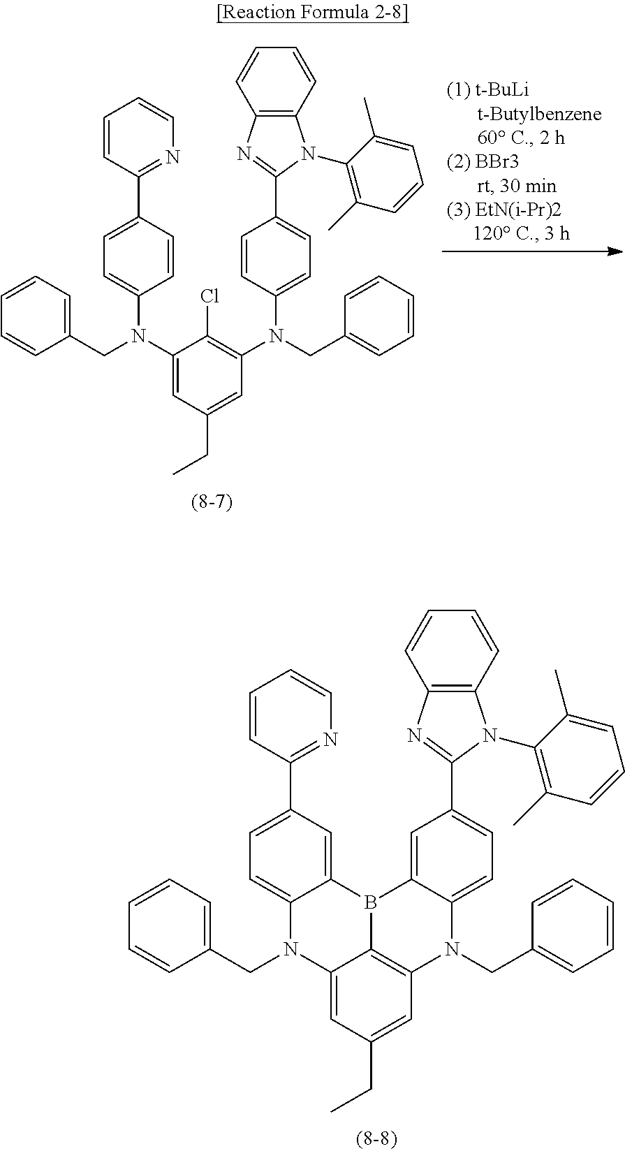


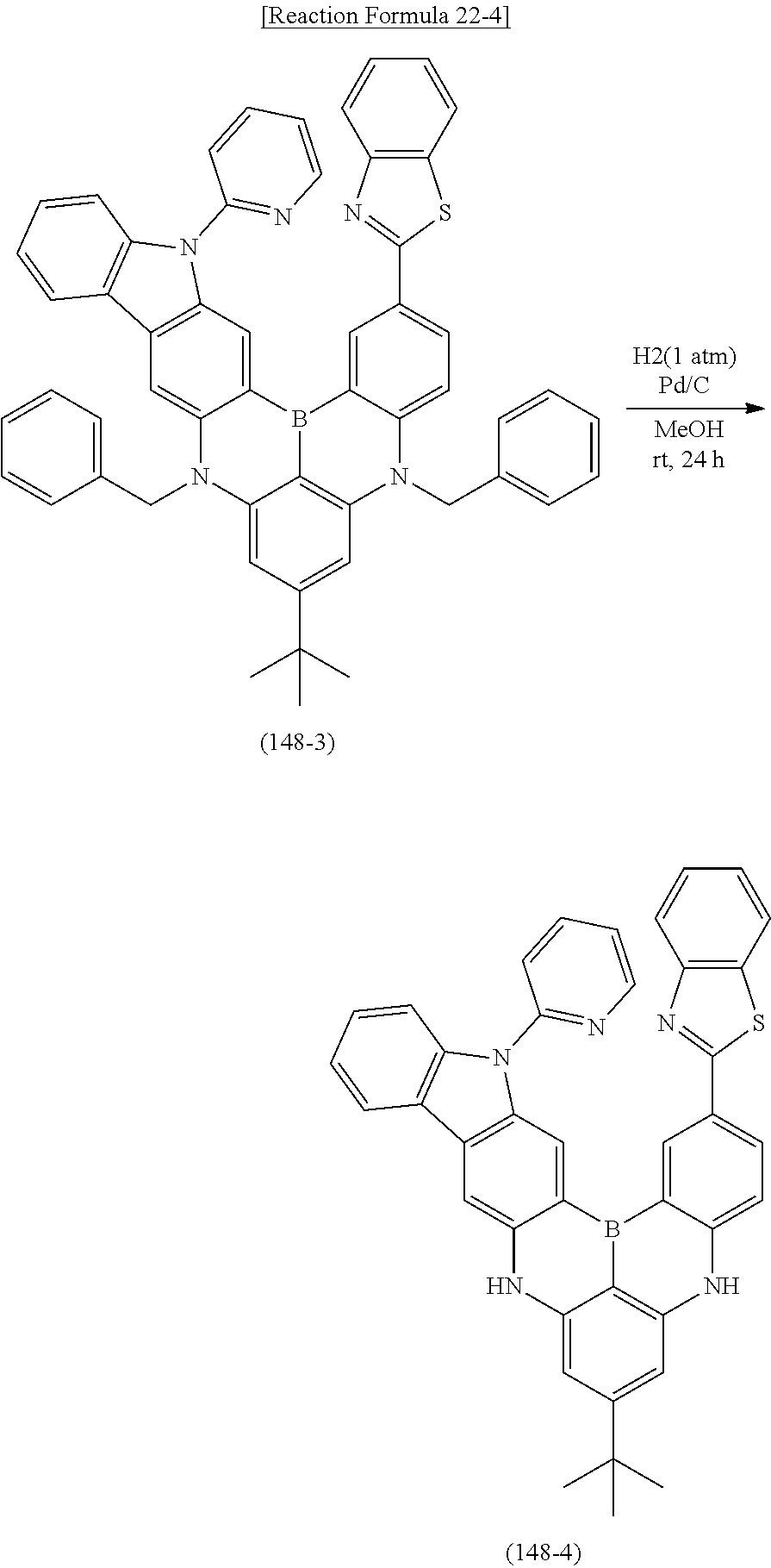


| TABLE 1 | ||||||
| Dopant | voltage [V] | Emax [%] | EQD [%] | LT95 [%] | ||
| Ref1 | Compound A | 4.25 | 100 | 100 | 100 | |
| Ex1 | Compound 1 | 4.33 | 143 | 125 | 121 | |
| Ex2 | Compound 8 | 4.31 | 144 | 121 | 120 | |
| Ex3 | Compound 12 | 4.26 | 148 | 125 | 122 | |
| Ex4 | Compound 31 | 4.31 | 139 | 119 | 119 | |
| Ex5 | Compound 38 | 4.32 | 135 | 122 | 125 | |
| Ex6 | Compound 96 | 4.30 | 133 | 121 | 126 | |
| | Compound | 102 | 4.29 | 151 | 138 | 120 |
| Ex8 | Compound 41 | 4.23 | 152 | 136 | 119 | |
| Ex9 | Compound 42 | 4.22 | 155 | 133 | 121 | |
| Ex10 | Compound 52 | 4.22 | 162 | 140 | 125 | |
| Ex11 | Compound 71 | 4.26 | 159 | 136 | 118 | |
| Ex12 | Compound 72 | 4.23 | 161 | 139 | 117 | |
| Ex13 | Compound 82 | 4.19 | 158 | 140 | 119 | |
| Ex14 | Compound 86 | 4.20 | 155 | 141 | 120 | |

| TABLE 2 | ||||||
| Dopant | voltage [V] | Emax [%] | EQD [%] | LT95 [%] | ||
| Ref2 | Compound B | 4.23 | 100 | 100 | 100 | |
| Ex15 | Compound 113 | 4.24 | 108 | 105 | 106 | |
| Ex16 | Compound 118 | 4.21 | 111 | 110 | 110 | |
| Ex17 | Compound 123 | 4.22 | 109 | 106 | 111 | |
| | Compound | 130 | 4.22 | 116 | 116 | 110 |
| | Compound | 132 | 4.25 | 121 | 118 | 115 |
| Ex20 | Compound 137 | 4.24 | 125 | 120 | 116 | |

| TABLE 3 | |||||
| Dopant | voltage [V] | Emax [%] | EQD [%] | LT95 [%] | |
| Ref3 | Compound C | 4.24 | 100 | 100 | 100 |
| Ex21 | Compound 143 | 4.22 | 110 | 105 | 105 |
| Ex22 | Compound 148 | 4.19 | 115 | 108 | 109 |
| Ex23 | Compound 153 | 4.26 | 109 | 110 | 109 |
| Ex24 | Compound 158 | 4.25 | 119 | 116 | 114 |
| Ex25 | Compound 162 | 4.23 | 124 | 118 | 112 |
| Ex26 | Compound 167 | 4.24 | 122 | 114 | 116 |

Claims (22)


Applications Claiming Priority (2)
| Application Number | Priority Date | Filing Date | Title |
|---|---|---|---|
| KR10-2019-0136398 | 2019-10-30 | ||
| KR1020190136398A KR102784367B1 (en) | 2019-10-30 | 2019-10-30 | Organic metal compound, organic light emitting diode and organic light emitting device including the organic metal compound |
Publications (2)
| Publication Number | Publication Date |
|---|---|
| US20210130382A1 US20210130382A1 (en) | 2021-05-06 |
| US12116377B2 true US12116377B2 (en) | 2024-10-15 |
Family
ID=75648863
Family Applications (1)
| Application Number | Title | Priority Date | Filing Date |
|---|---|---|---|
| US17/082,416 Active 2042-03-30 US12116377B2 (en) | 2019-10-30 | 2020-10-28 | Organometallic compound, organic light emitting diode and organic light emitting device including the same |
Country Status (3)
| Country | Link |
|---|---|
| US (1) | US12116377B2 (en) |
| KR (1) | KR102784367B1 (en) |
| CN (1) | CN112745354B (en) |
Families Citing this family (6)
| Publication number | Priority date | Publication date | Assignee | Title |
|---|---|---|---|---|
| US12250872B2 (en) | 2019-02-22 | 2025-03-11 | Universal Display Corporation | Organic electroluminescent materials and devices |
| US12426495B2 (en) | 2020-01-28 | 2025-09-23 | Universal Display Corporation | Organic electroluminescent materials and devices |
| JP2023050138A (en) * | 2021-09-29 | 2023-04-10 | 住友化学株式会社 | Light-emitting element |
| JP2023050136A (en) * | 2021-09-29 | 2023-04-10 | 住友化学株式会社 | Composition and light emitting element containing the same |
| CN115160379B (en) * | 2022-08-01 | 2024-02-02 | 浙江工业大学 | Circularly polarized luminescent material and application, luminescent display device and display device |
| CN116120353A (en) * | 2023-01-16 | 2023-05-16 | 北京八亿时空液晶科技股份有限公司 | Carbazole derivative containing boron atom and application thereof |
Citations (13)
| Publication number | Priority date | Publication date | Assignee | Title |
|---|---|---|---|---|
| US20060188745A1 (en) * | 2005-02-23 | 2006-08-24 | Eastman Kodak Company | Tandem OLED having an organic intermediate connector |
| US20140014922A1 (en) * | 2012-07-10 | 2014-01-16 | Universal Display Corporation | Phosphorescent emitters containing dibenzo[1,4]azaborinine structure |
| US20140070196A1 (en) * | 2012-09-12 | 2014-03-13 | Lg Display Co., Ltd. | Organic light emitting display device |
| US20140084269A1 (en) * | 2012-09-26 | 2014-03-27 | Universal Display Corporation | Three stack hybrid white oled for enhanced efficiency and lifetime |
| US20150188083A1 (en) | 2013-12-30 | 2015-07-02 | Lg Display Co., Ltd. | Organic light emitting display device and manufacturing method thereof |
| US20160181350A1 (en) * | 2014-12-18 | 2016-06-23 | Samsung Display Co., Ltd. | Organic light-emitting display apparatus and method of manufacturing the same |
| US20180166647A1 (en) | 2016-12-12 | 2018-06-14 | Lg Display Co., Ltd. | Organic compound and light emitting diode and organic light emitting diode display device using the same |
| US20180305384A1 (en) | 2017-04-21 | 2018-10-25 | Universal Display Corporation | Organic electroluminescent materials and devices |
| US20180375036A1 (en) | 2017-06-23 | 2018-12-27 | Universal Display Corporation | Organic electroluminescent materials and devices |
| US20200168816A1 (en) | 2018-11-26 | 2020-05-28 | Samsung Display Co., Ltd. | Organometallic compound and organic light-emitting device including the same |
| US20200203634A1 (en) | 2018-12-20 | 2020-06-25 | Samsung Display Co., Ltd. | Organometallic compound and organic light-emitting device including the same |
| US20200274079A1 (en) | 2019-02-22 | 2020-08-27 | Universal Display Corporation | Organic electroluminescent materials and devices |
| US20200388774A1 (en) | 2019-02-22 | 2020-12-10 | Universal Display Corporation | Organic electroluminescent materials and devices |
Family Cites Families (1)
| Publication number | Priority date | Publication date | Assignee | Title |
|---|---|---|---|---|
| US9879039B2 (en) * | 2015-06-03 | 2018-01-30 | Arizona Board Of Regents On Behalf Of Arizona State University | Tetradentate and octahedral metal complexes containing naphthyridinocarbazole and its analogues |
-
2019
- 2019-10-30 KR KR1020190136398A patent/KR102784367B1/en active Active
-
2020
- 2020-10-28 US US17/082,416 patent/US12116377B2/en active Active
- 2020-10-30 CN CN202011191983.3A patent/CN112745354B/en active Active
Patent Citations (16)
| Publication number | Priority date | Publication date | Assignee | Title |
|---|---|---|---|---|
| US20060188745A1 (en) * | 2005-02-23 | 2006-08-24 | Eastman Kodak Company | Tandem OLED having an organic intermediate connector |
| US20140014922A1 (en) * | 2012-07-10 | 2014-01-16 | Universal Display Corporation | Phosphorescent emitters containing dibenzo[1,4]azaborinine structure |
| US9231218B2 (en) | 2012-07-10 | 2016-01-05 | Universal Display Corporation | Phosphorescent emitters containing dibenzo[1,4]azaborinine structure |
| US20140070196A1 (en) * | 2012-09-12 | 2014-03-13 | Lg Display Co., Ltd. | Organic light emitting display device |
| US20140084269A1 (en) * | 2012-09-26 | 2014-03-27 | Universal Display Corporation | Three stack hybrid white oled for enhanced efficiency and lifetime |
| US20150188083A1 (en) | 2013-12-30 | 2015-07-02 | Lg Display Co., Ltd. | Organic light emitting display device and manufacturing method thereof |
| US20160181350A1 (en) * | 2014-12-18 | 2016-06-23 | Samsung Display Co., Ltd. | Organic light-emitting display apparatus and method of manufacturing the same |
| US20180166647A1 (en) | 2016-12-12 | 2018-06-14 | Lg Display Co., Ltd. | Organic compound and light emitting diode and organic light emitting diode display device using the same |
| US20180305384A1 (en) | 2017-04-21 | 2018-10-25 | Universal Display Corporation | Organic electroluminescent materials and devices |
| KR20180118559A (en) | 2017-04-21 | 2018-10-31 | 유니버셜 디스플레이 코포레이션 | Organic electroluminescent materials and devices |
| US20180375036A1 (en) | 2017-06-23 | 2018-12-27 | Universal Display Corporation | Organic electroluminescent materials and devices |
| KR20190000812A (en) | 2017-06-23 | 2019-01-03 | 유니버셜 디스플레이 코포레이션 | Organic electroluminescent materials and devices |
| US20200168816A1 (en) | 2018-11-26 | 2020-05-28 | Samsung Display Co., Ltd. | Organometallic compound and organic light-emitting device including the same |
| US20200203634A1 (en) | 2018-12-20 | 2020-06-25 | Samsung Display Co., Ltd. | Organometallic compound and organic light-emitting device including the same |
| US20200274079A1 (en) | 2019-02-22 | 2020-08-27 | Universal Display Corporation | Organic electroluminescent materials and devices |
| US20200388774A1 (en) | 2019-02-22 | 2020-12-10 | Universal Display Corporation | Organic electroluminescent materials and devices |
Non-Patent Citations (3)
| Title |
|---|
| Cebrian et al., "Recent advances in phosphorescent platinum complexes for organic light-emitting diodes," Beilstein J. Org. Chem. 14:1459-1481, 2018. |
| Office Action dated Dec. 12, 2023, in related U.S. Appl. No. 17/009,609. |
| U.S. Office Action dated Mar. 2, 2023, in related technology U.S. Appl. No. 17/009,609. |
Also Published As
| Publication number | Publication date |
|---|---|
| CN112745354A (en) | 2021-05-04 |
| CN112745354B (en) | 2024-07-19 |
| KR102784367B1 (en) | 2025-03-19 |
| KR20210051303A (en) | 2021-05-10 |
| US20210130382A1 (en) | 2021-05-06 |
Similar Documents
| Publication | Publication Date | Title |
|---|---|---|
| US12116377B2 (en) | Organometallic compound, organic light emitting diode and organic light emitting device including the same | |
| US11950500B2 (en) | Organic light emitting diode and organic light emitting device having thereof | |
| US12144242B2 (en) | Organic metal compound, organic light emitting diode and organic light emitting device having the compound | |
| US20220020929A1 (en) | Organic light emitting diode and organic light emitting device having thereof | |
| US12161046B2 (en) | Organic light emitting diode and organic light emitting device having thereof | |
| US12284907B2 (en) | Organic light emitting diode and organic light emitting device having thereof | |
| US11655219B2 (en) | Organic compound, organic light emitting diode and organic light emitting device including the compound | |
| US20230209859A1 (en) | Organic light emitting diode and organic light emitting display device including the same | |
| US9666809B2 (en) | Compound and organic light-emitting device including the same | |
| US20220223803A1 (en) | Organic metal compound, organic light emitting diode and organic light emitting device having the compound | |
| US20250338713A1 (en) | Organic light emitting diode and organic light emitting device including the same | |
| US12550608B2 (en) | Organic light emitting diode and organic light emitting device including the same | |
| US12433159B2 (en) | Organic compound, and organic light emitting diode and organic light emitting device including the same | |
| US20240251652A1 (en) | Organometallic compound, organic light emitting diode and organic light emitting device including the same | |
| US12446458B2 (en) | Organometallic compound, organic light emitting diode and organic light emitting device including the organometallic compound | |
| US20240180034A1 (en) | Organic light emitting diode and organic light emitting device including the same | |
| US12527218B2 (en) | Organic compound, organic light emitting diode and organic light emitting device including the organic compound | |
| US20240254152A1 (en) | Organometallic compound, organic light emitting diode and organic light emitting device including the same | |
| US20240246996A1 (en) | Organic compound, organic light emitting diode and organic light emitting device including the same | |
| US20240246997A1 (en) | Organic compound, organic light emitting diode and organic light emitting device including the same | |
| US20230217814A1 (en) | Organic compound and organic light emitting device including the same | |
| US20240244951A1 (en) | Organometallic compound, organic light emitting diode and organic light emitting device including the same | |
| US20240251653A1 (en) | Organometallic compound, organic light emitting diode and organic light emitting device including the same | |
| US20250188105A1 (en) | Organometallic compound, organic light emitting diode and organic light emitting device including the same | |
| US20240218003A1 (en) | Organometallic compound, organic light emitting diode and organic light emitting device having the compound |
Legal Events
| Date | Code | Title | Description |
|---|---|---|---|
| AS | Assignment |
Owner name: LG DISPLAY CO., LTD., KOREA, REPUBLIC OF Free format text: ASSIGNMENT OF ASSIGNORS INTEREST;ASSIGNORS:PARK, HEE-JUN;KIM, DO-HAN;KANG, HYE-SEUNG;AND OTHERS;SIGNING DATES FROM 20200911 TO 20200923;REEL/FRAME:054248/0534 |
|
| FEPP | Fee payment procedure |
Free format text: ENTITY STATUS SET TO UNDISCOUNTED (ORIGINAL EVENT CODE: BIG.); ENTITY STATUS OF PATENT OWNER: LARGE ENTITY |
|
| STPP | Information on status: patent application and granting procedure in general |
Free format text: APPLICATION DISPATCHED FROM PREEXAM, NOT YET DOCKETED |
|
| STPP | Information on status: patent application and granting procedure in general |
Free format text: DOCKETED NEW CASE - READY FOR EXAMINATION |
|
| STPP | Information on status: patent application and granting procedure in general |
Free format text: NON FINAL ACTION MAILED |
|
| STPP | Information on status: patent application and granting procedure in general |
Free format text: FINAL REJECTION MAILED |
|
| STPP | Information on status: patent application and granting procedure in general |
Free format text: DOCKETED NEW CASE - READY FOR EXAMINATION |
|
| STPP | Information on status: patent application and granting procedure in general |
Free format text: NON FINAL ACTION MAILED |
|
| STPP | Information on status: patent application and granting procedure in general |
Free format text: RESPONSE TO NON-FINAL OFFICE ACTION ENTERED AND FORWARDED TO EXAMINER |
|
| STPP | Information on status: patent application and granting procedure in general |
Free format text: NOTICE OF ALLOWANCE MAILED -- APPLICATION RECEIVED IN OFFICE OF PUBLICATIONS |
|
| STPP | Information on status: patent application and granting procedure in general |
Free format text: PUBLICATIONS -- ISSUE FEE PAYMENT RECEIVED |
|
| STPP | Information on status: patent application and granting procedure in general |
Free format text: PUBLICATIONS -- ISSUE FEE PAYMENT VERIFIED |
|
| STCF | Information on status: patent grant |
Free format text: PATENTED CASE |