US12107168B2 - Independent gate length tunability for stacked transistors - Google Patents
Independent gate length tunability for stacked transistors Download PDFInfo
- Publication number
- US12107168B2 US12107168B2 US17/411,618 US202117411618A US12107168B2 US 12107168 B2 US12107168 B2 US 12107168B2 US 202117411618 A US202117411618 A US 202117411618A US 12107168 B2 US12107168 B2 US 12107168B2
- Authority
- US
- United States
- Prior art keywords
- semiconductor
- layer
- gate
- sacrificial
- dielectric
- Prior art date
- Legal status (The legal status is an assumption and is not a legal conclusion. Google has not performed a legal analysis and makes no representation as to the accuracy of the status listed.)
- Active, expires
Links
Images


Classifications
-
- H—ELECTRICITY
- H10—SEMICONDUCTOR DEVICES; ELECTRIC SOLID-STATE DEVICES NOT OTHERWISE PROVIDED FOR
- H10D—INORGANIC ELECTRIC SEMICONDUCTOR DEVICES
- H10D30/00—Field-effect transistors [FET]
- H10D30/60—Insulated-gate field-effect transistors [IGFET]
- H10D30/67—Thin-film transistors [TFT]
- H10D30/6757—Thin-film transistors [TFT] characterised by the structure of the channel, e.g. transverse or longitudinal shape or doping profile
-
- H01L29/7855—
-
- H—ELECTRICITY
- H10—SEMICONDUCTOR DEVICES; ELECTRIC SOLID-STATE DEVICES NOT OTHERWISE PROVIDED FOR
- H10D—INORGANIC ELECTRIC SEMICONDUCTOR DEVICES
- H10D30/00—Field-effect transistors [FET]
- H10D30/60—Insulated-gate field-effect transistors [IGFET]
- H10D30/62—Fin field-effect transistors [FinFET]
- H10D30/6215—Fin field-effect transistors [FinFET] having multiple independently-addressable gate electrodes
-
- H01L29/0665—
-
- H01L29/0847—
-
- H01L29/1033—
-
- H—ELECTRICITY
- H10—SEMICONDUCTOR DEVICES; ELECTRIC SOLID-STATE DEVICES NOT OTHERWISE PROVIDED FOR
- H10D—INORGANIC ELECTRIC SEMICONDUCTOR DEVICES
- H10D30/00—Field-effect transistors [FET]
- H10D30/01—Manufacture or treatment
- H10D30/014—Manufacture or treatment of FETs having zero-dimensional [0D] or one-dimensional [1D] channels, e.g. quantum wire FETs, single-electron transistors [SET] or Coulomb blockade transistors
-
- H—ELECTRICITY
- H10—SEMICONDUCTOR DEVICES; ELECTRIC SOLID-STATE DEVICES NOT OTHERWISE PROVIDED FOR
- H10D—INORGANIC ELECTRIC SEMICONDUCTOR DEVICES
- H10D30/00—Field-effect transistors [FET]
- H10D30/40—FETs having zero-dimensional [0D], one-dimensional [1D] or two-dimensional [2D] charge carrier gas channels
- H10D30/43—FETs having zero-dimensional [0D], one-dimensional [1D] or two-dimensional [2D] charge carrier gas channels having one-dimensional [1D] charge carrier gas channels, e.g. quantum wire FETs or transistors having 1D quantum-confined channels
-
- H—ELECTRICITY
- H10—SEMICONDUCTOR DEVICES; ELECTRIC SOLID-STATE DEVICES NOT OTHERWISE PROVIDED FOR
- H10D—INORGANIC ELECTRIC SEMICONDUCTOR DEVICES
- H10D30/00—Field-effect transistors [FET]
- H10D30/60—Insulated-gate field-effect transistors [IGFET]
- H10D30/67—Thin-film transistors [TFT]
- H10D30/6729—Thin-film transistors [TFT] characterised by the electrodes
- H10D30/673—Thin-film transistors [TFT] characterised by the electrodes characterised by the shapes, relative sizes or dispositions of the gate electrodes
- H10D30/6735—Thin-film transistors [TFT] characterised by the electrodes characterised by the shapes, relative sizes or dispositions of the gate electrodes having gates fully surrounding the channels, e.g. gate-all-around
-
- H—ELECTRICITY
- H10—SEMICONDUCTOR DEVICES; ELECTRIC SOLID-STATE DEVICES NOT OTHERWISE PROVIDED FOR
- H10D—INORGANIC ELECTRIC SEMICONDUCTOR DEVICES
- H10D62/00—Semiconductor bodies, or regions thereof, of devices having potential barriers
- H10D62/10—Shapes, relative sizes or dispositions of the regions of the semiconductor bodies; Shapes of the semiconductor bodies
- H10D62/117—Shapes of semiconductor bodies
- H10D62/118—Nanostructure semiconductor bodies
- H10D62/119—Nanowire, nanosheet or nanotube semiconductor bodies
- H10D62/121—Nanowire, nanosheet or nanotube semiconductor bodies oriented parallel to substrates
-
- H—ELECTRICITY
- H10—SEMICONDUCTOR DEVICES; ELECTRIC SOLID-STATE DEVICES NOT OTHERWISE PROVIDED FOR
- H10D—INORGANIC ELECTRIC SEMICONDUCTOR DEVICES
- H10D62/00—Semiconductor bodies, or regions thereof, of devices having potential barriers
- H10D62/10—Shapes, relative sizes or dispositions of the regions of the semiconductor bodies; Shapes of the semiconductor bodies
- H10D62/13—Semiconductor regions connected to electrodes carrying current to be rectified, amplified or switched, e.g. source or drain regions
- H10D62/149—Source or drain regions of field-effect devices
- H10D62/151—Source or drain regions of field-effect devices of IGFETs
-
- H—ELECTRICITY
- H10—SEMICONDUCTOR DEVICES; ELECTRIC SOLID-STATE DEVICES NOT OTHERWISE PROVIDED FOR
- H10D—INORGANIC ELECTRIC SEMICONDUCTOR DEVICES
- H10D62/00—Semiconductor bodies, or regions thereof, of devices having potential barriers
- H10D62/10—Shapes, relative sizes or dispositions of the regions of the semiconductor bodies; Shapes of the semiconductor bodies
- H10D62/17—Semiconductor regions connected to electrodes not carrying current to be rectified, amplified or switched, e.g. channel regions
- H10D62/213—Channel regions of field-effect devices
- H10D62/221—Channel regions of field-effect devices of FETs
- H10D62/235—Channel regions of field-effect devices of FETs of IGFETs
-
- H—ELECTRICITY
- H10—SEMICONDUCTOR DEVICES; ELECTRIC SOLID-STATE DEVICES NOT OTHERWISE PROVIDED FOR
- H10D—INORGANIC ELECTRIC SEMICONDUCTOR DEVICES
- H10D64/00—Electrodes of devices having potential barriers
- H10D64/01—Manufacture or treatment
- H10D64/017—Manufacture or treatment using dummy gates in processes wherein at least parts of the final gates are self-aligned to the dummy gates, i.e. replacement gate processes
-
- H—ELECTRICITY
- H10—SEMICONDUCTOR DEVICES; ELECTRIC SOLID-STATE DEVICES NOT OTHERWISE PROVIDED FOR
- H10D—INORGANIC ELECTRIC SEMICONDUCTOR DEVICES
- H10D84/00—Integrated devices formed in or on semiconductor substrates that comprise only semiconducting layers, e.g. on Si wafers or on GaAs-on-Si wafers
- H10D84/01—Manufacture or treatment
- H10D84/0123—Integrating together multiple components covered by H10D12/00 or H10D30/00, e.g. integrating multiple IGBTs
- H10D84/0126—Integrating together multiple components covered by H10D12/00 or H10D30/00, e.g. integrating multiple IGBTs the components including insulated gates, e.g. IGFETs
- H10D84/0135—Manufacturing their gate conductors
- H10D84/0142—Manufacturing their gate conductors the gate conductors having different shapes or dimensions
-
- H—ELECTRICITY
- H10—SEMICONDUCTOR DEVICES; ELECTRIC SOLID-STATE DEVICES NOT OTHERWISE PROVIDED FOR
- H10D—INORGANIC ELECTRIC SEMICONDUCTOR DEVICES
- H10D84/00—Integrated devices formed in or on semiconductor substrates that comprise only semiconducting layers, e.g. on Si wafers or on GaAs-on-Si wafers
- H10D84/01—Manufacture or treatment
- H10D84/0123—Integrating together multiple components covered by H10D12/00 or H10D30/00, e.g. integrating multiple IGBTs
- H10D84/0126—Integrating together multiple components covered by H10D12/00 or H10D30/00, e.g. integrating multiple IGBTs the components including insulated gates, e.g. IGFETs
- H10D84/0165—Integrating together multiple components covered by H10D12/00 or H10D30/00, e.g. integrating multiple IGBTs the components including insulated gates, e.g. IGFETs the components including complementary IGFETs, e.g. CMOS devices
- H10D84/0172—Manufacturing their gate conductors
- H10D84/0179—Manufacturing their gate conductors the gate conductors having different shapes or dimensions
-
- H—ELECTRICITY
- H10—SEMICONDUCTOR DEVICES; ELECTRIC SOLID-STATE DEVICES NOT OTHERWISE PROVIDED FOR
- H10D—INORGANIC ELECTRIC SEMICONDUCTOR DEVICES
- H10D84/00—Integrated devices formed in or on semiconductor substrates that comprise only semiconducting layers, e.g. on Si wafers or on GaAs-on-Si wafers
- H10D84/01—Manufacture or treatment
- H10D84/02—Manufacture or treatment characterised by using material-based technologies
- H10D84/03—Manufacture or treatment characterised by using material-based technologies using Group IV technology, e.g. silicon technology or silicon-carbide [SiC] technology
- H10D84/038—Manufacture or treatment characterised by using material-based technologies using Group IV technology, e.g. silicon technology or silicon-carbide [SiC] technology using silicon technology, e.g. SiGe
-
- H—ELECTRICITY
- H10—SEMICONDUCTOR DEVICES; ELECTRIC SOLID-STATE DEVICES NOT OTHERWISE PROVIDED FOR
- H10D—INORGANIC ELECTRIC SEMICONDUCTOR DEVICES
- H10D84/00—Integrated devices formed in or on semiconductor substrates that comprise only semiconducting layers, e.g. on Si wafers or on GaAs-on-Si wafers
- H10D84/80—Integrated devices formed in or on semiconductor substrates that comprise only semiconducting layers, e.g. on Si wafers or on GaAs-on-Si wafers characterised by the integration of at least one component covered by groups H10D12/00 or H10D30/00, e.g. integration of IGFETs
- H10D84/82—Integrated devices formed in or on semiconductor substrates that comprise only semiconducting layers, e.g. on Si wafers or on GaAs-on-Si wafers characterised by the integration of at least one component covered by groups H10D12/00 or H10D30/00, e.g. integration of IGFETs of only field-effect components
- H10D84/83—Integrated devices formed in or on semiconductor substrates that comprise only semiconducting layers, e.g. on Si wafers or on GaAs-on-Si wafers characterised by the integration of at least one component covered by groups H10D12/00 or H10D30/00, e.g. integration of IGFETs of only field-effect components of only insulated-gate FETs [IGFET]
- H10D84/85—Complementary IGFETs, e.g. CMOS
-
- H—ELECTRICITY
- H10—SEMICONDUCTOR DEVICES; ELECTRIC SOLID-STATE DEVICES NOT OTHERWISE PROVIDED FOR
- H10D—INORGANIC ELECTRIC SEMICONDUCTOR DEVICES
- H10D88/00—Three-dimensional [3D] integrated devices
-
- H—ELECTRICITY
- H10—SEMICONDUCTOR DEVICES; ELECTRIC SOLID-STATE DEVICES NOT OTHERWISE PROVIDED FOR
- H10D—INORGANIC ELECTRIC SEMICONDUCTOR DEVICES
- H10D88/00—Three-dimensional [3D] integrated devices
- H10D88/01—Manufacture or treatment
-
- B—PERFORMING OPERATIONS; TRANSPORTING
- B82—NANOTECHNOLOGY
- B82Y—SPECIFIC USES OR APPLICATIONS OF NANOSTRUCTURES; MEASUREMENT OR ANALYSIS OF NANOSTRUCTURES; MANUFACTURE OR TREATMENT OF NANOSTRUCTURES
- B82Y10/00—Nanotechnology for information processing, storage or transmission, e.g. quantum computing or single electron logic
-
- H—ELECTRICITY
- H10—SEMICONDUCTOR DEVICES; ELECTRIC SOLID-STATE DEVICES NOT OTHERWISE PROVIDED FOR
- H10D—INORGANIC ELECTRIC SEMICONDUCTOR DEVICES
- H10D84/00—Integrated devices formed in or on semiconductor substrates that comprise only semiconducting layers, e.g. on Si wafers or on GaAs-on-Si wafers
- H10D84/01—Manufacture or treatment
- H10D84/0123—Integrating together multiple components covered by H10D12/00 or H10D30/00, e.g. integrating multiple IGBTs
- H10D84/0126—Integrating together multiple components covered by H10D12/00 or H10D30/00, e.g. integrating multiple IGBTs the components including insulated gates, e.g. IGFETs
- H10D84/0128—Manufacturing their channels
-
- H—ELECTRICITY
- H10—SEMICONDUCTOR DEVICES; ELECTRIC SOLID-STATE DEVICES NOT OTHERWISE PROVIDED FOR
- H10D—INORGANIC ELECTRIC SEMICONDUCTOR DEVICES
- H10D84/00—Integrated devices formed in or on semiconductor substrates that comprise only semiconducting layers, e.g. on Si wafers or on GaAs-on-Si wafers
- H10D84/01—Manufacture or treatment
- H10D84/0123—Integrating together multiple components covered by H10D12/00 or H10D30/00, e.g. integrating multiple IGBTs
- H10D84/0126—Integrating together multiple components covered by H10D12/00 or H10D30/00, e.g. integrating multiple IGBTs the components including insulated gates, e.g. IGFETs
- H10D84/0165—Integrating together multiple components covered by H10D12/00 or H10D30/00, e.g. integrating multiple IGBTs the components including insulated gates, e.g. IGFETs the components including complementary IGFETs, e.g. CMOS devices
- H10D84/0167—Manufacturing their channels
-
- H—ELECTRICITY
- H10—SEMICONDUCTOR DEVICES; ELECTRIC SOLID-STATE DEVICES NOT OTHERWISE PROVIDED FOR
- H10D—INORGANIC ELECTRIC SEMICONDUCTOR DEVICES
- H10D86/00—Integrated devices formed in or on insulating or conducting substrates, e.g. formed in silicon-on-insulator [SOI] substrates or on stainless steel or glass substrates
- H10D86/201—Integrated devices formed in or on insulating or conducting substrates, e.g. formed in silicon-on-insulator [SOI] substrates or on stainless steel or glass substrates the substrates comprising an insulating layer on a semiconductor body, e.g. SOI
- H10D86/215—Integrated devices formed in or on insulating or conducting substrates, e.g. formed in silicon-on-insulator [SOI] substrates or on stainless steel or glass substrates the substrates comprising an insulating layer on a semiconductor body, e.g. SOI comprising FinFETs
Definitions
- the present application relates to semiconductor technology, and more particularly to a semiconductor structure having stacked field effect transistors (FETs) with different and tunable gate lengths.
- FETs field effect transistors
- CMOS Complementary metal oxide semiconductor
- FETs are commonly used for FETs as part of advanced integrated circuits, such as central processing units, memory, storage devices, and the like.
- stacked FETs help achieve a reduced FET device footprint, while maintaining FET device performance.
- a stacked FET is a structure in which one FET is vertically stacked atop another FET.
- a p-type FET can be stacked above an n-type FET, or an n-type FET can be stacked above a p-type FET.
- Stacked FETs use less surface area of a die than conventional FETs and is needed with shrinking design rules.
- Vt threshold voltage
- tunablity by different gate lengths is generally needed if the stacked FETs are the same; a p-type FET has more Vt roll-off than an n-type FET so shrinking a p-type FET independently could achieve a lower Vt.
- n-type and p-type FETs when two types of FETs (i.e., n-type and p-type FETs) are stacked, a different gate length is required to maximize the benefits for each of the FETs.
- one FET could be located on a semiconductor fin (i.e., FinFET), while another FET can be wrapped around a nanosheet stack of semiconductor channel material nanosheets (i.e., nanosheet FET). More benefits can be achieved when the nanosheet FET is designed to have a smaller gate length than the FinFET because of better electrostatics coming from the nanosheet FET.
- a stacked FET structure having independently tuned gate lengths is provided to maximize the benefit of each FET within the stacked FET structure.
- a vertically stacked FET structure is provided in which a bottom FET has a different gate length than a top FET.
- a dielectric spacer can be present laterally adjacent to the bottom FET and the top FET.
- the dielectric spacer can have a first portion that is located laterally adjacent to the bottom FET that has a different thickness than a second portion of the dielectric spacer that is located laterally adjacent the top FET.
- a semiconductor structure in one aspect of the present application, includes a bottom FET and a top FET stacked in a vertical manner one atop the other, wherein the bottom FET has a first gate length, and the top FET has a second gate length that differs from the first gate length.
- each of the bottom FET and the top FET is one of a planar FET, a FinFET, and a nanosheet FET.
- the bottom FET is a nanosheet FET and the top FET is a FinFET.
- the bottom FET is a FinFET
- the top FET is a nanosheet FET.
- both the bottom and top FETs are nanosheet FETs.
- both the bottom and top FETs are planar FETs (n-type FET and p-type FET).
- the first gate length can be greater than the second gate length.
- a dielectric spacer that is present along sidewalls of the bottom FET (e.g., nanosheet FET) and the top FET (e.g., FinFET) has a first portion located laterally adjacent to the bottom FET (e.g., nanosheet FET) having a first thickness, and a second portion located laterally adjacent to the top FET (e.g., FinFET) having a second thickness that is greater than the first thickness.
- the first gate length is less than the second gate length.
- a dielectric spacer that is present along sidewalls of the bottom FET (e.g., nanosheet FET) and top FET (e.g., FinFET) has a first portion located laterally adjacent to the bottom FET (e.g., nanosheet FET) having a first thickness, and a second portion located laterally adjacent to the top FET (e.g., FinFET) having a second thickness that is less than the first thickness.
- methods of forming a semiconductor structure including a bottom FET and a top FET stacked in a vertical manner one atop the other are provided in which the bottom FET has a first gate length and the top FET has a second gate length that differs from the first gate length.
- methods of forming a semiconductor structure including a FinFET and a nanosheet FET stacked in a vertical manner one atop the other are provided in which the FinFET has a first gate length and the nanosheet FET has a second gate length that differs from the first gate length.
- FIG. 1 is a schematic top-down view showing an exemplary device layout that can be employed in the present application, the device layout including a functional gate structure that straddles over a pair of neighboring semiconductor fins.
- FIG. 2 A is a cross sectional view of an exemplary semiconductor structure that can be employed in the present application and through Y-Y shown in FIG. 1 , the exemplary structure includes a material stack of alternating layers of sacrificial semiconductor material and semiconductor channel material located on a bottom isolation layer that is located on a semiconductor substrate, a top isolation layer located on the material stack, at least one semiconductor channel material structure located on the top isolation layer, and a sacrificial gate material-containing stack including at least a first sacrificial gate material layer located on each semiconductor fin, and laterally adjacent to the material stack.
- FIG. 2 B is a cross sectional view of an exemplary semiconductor structure that can be employed in the present application and through X-X shown in FIG. 1 , the exemplary structure includes a material stack of alternating layers of sacrificial semiconductor material and semiconductor channel material located on a bottom isolation layer that is located on a semiconductor substrate, a top isolation layer located on the material stack, at least one semiconductor channel material structure located on the top isolation layer, and a sacrificial gate material-containing stack including at least a first sacrificial gate material layer located on each semiconductor fin, and laterally adjacent to the material stack.
- FIG. 2 C is a cross sectional view of an exemplary semiconductor structure that can be employed in the present application and through X 1 -X 1 shown in FIG. 1 , the exemplary structure includes a material stack of alternating layers of sacrificial semiconductor material and semiconductor channel material located on a bottom isolation layer that is located on a semiconductor substrate, a top isolation layer located on the material stack, at least one semiconductor channel material structure located on the top isolation layer, and a sacrificial gate material-containing stack including at least a first sacrificial gate material layer located on each semiconductor fin, and laterally adjacent to the material stack.
- FIG. 3 A is a cross sectional view of the exemplary semiconductor structure shown in FIG. 2 A after recessing the first sacrificial gate material layer.
- FIG. 3 B is a cross sectional view of the exemplary semiconductor structure shown in FIG. 2 B after recessing the first sacrificial gate material layer.
- FIG. 3 C is a cross sectional view of the exemplary semiconductor structure shown in FIG. 2 C after recessing the first sacrificial gate material layer.
- FIG. 4 A is a cross sectional view of the exemplary semiconductor structure shown in FIG. 3 A after forming a second sacrificial gate material layer on the recessed first sacrificial gate material layer.
- FIG. 4 B is a cross sectional view of the exemplary semiconductor structure shown in FIG. 3 B after forming a second sacrificial gate material layer on the recessed first sacrificial gate material layer.
- FIG. 4 C is a cross sectional view of the exemplary semiconductor structure shown in FIG. 3 C after forming a second sacrificial gate material layer on the recessed first sacrificial gate material layer.
- FIG. 5 A is a cross sectional view of the exemplary semiconductor structure shown in FIG. 4 A after patterning the second sacrificial gate material layer and the recessed first sacrificial gate material layer to provide a sacrificial gate material-containing pillar containing a remaining portion of the second sacrificial gate material layer and a remaining portion of the recessed first sacrificial gate material layer.
- FIG. 5 B is a cross sectional view of the exemplary semiconductor structure shown in FIG. 4 B after patterning the second sacrificial gate material layer and the recessed first sacrificial gate material layer to provide a sacrificial gate material-containing pillar containing a remaining portion of the second sacrificial gate material layer and a remaining portion of the recessed first sacrificial gate material layer.
- FIG. 5 C is a cross sectional view of the exemplary semiconductor structure shown in FIG. 4 C after patterning the second sacrificial gate material layer and the recessed first sacrificial gate material layer to provide a sacrificial gate material-containing pillar containing a remaining portion of the second sacrificial gate material layer and a remaining portion of the recessed first sacrificial gate material layer.
- FIG. 6 A is a cross sectional view of the exemplary semiconductor structure shown in FIG. 5 A after thinning the recessed first sacrificial gate material layer to provide a modified sacrificial gate material-containing pillar containing the remaining portion of the second sacrificial gate material layer and a remaining thinned portion of the recessed first sacrificial gate material layer.
- FIG. 6 B is a cross sectional view of the exemplary semiconductor structure shown in FIG. 5 B after thinning the recessed first sacrificial gate material layer to provide a modified sacrificial gate material-containing pillar containing the remaining portion of the second sacrificial gate material layer and a remaining thinned portion of the recessed first sacrificial gate material layer.
- FIG. 6 C is a cross sectional view of the exemplary semiconductor structure shown in FIG. 5 C after thinning recessed first sacrificial gate material layer to provide a modified sacrificial gate material-containing pillar containing the remaining portion of the second sacrificial gate material layer and a remaining thinned portion of the recessed first sacrificial gate material layer.
- FIG. 7 A is a cross sectional view of the exemplary semiconductor structure shown in FIG. 6 A after forming a dielectric spacer along the physically exposed sidewall of the modified sacrificial gate material-containing pillar.
- FIG. 7 B is a cross sectional view of the exemplary semiconductor structure shown in FIG. 6 B after forming a dielectric spacer along the physically exposed sidewall of the modified sacrificial gate material-containing pillar.
- FIG. 7 C is a cross sectional view of the exemplary semiconductor structure shown in FIG. 6 C after forming a dielectric spacer along the physically exposed sidewall of the modified sacrificial gate material-containing pillar.
- FIG. 8 A is a cross sectional view of the exemplary semiconductor structure shown in FIG. 7 A after further device processing including forming a semiconductor fin from each semiconductor channel material structure and a nanosheet stack containing alternating nanosheets of sacrificial semiconductor material and semiconductor channel material from the material stack, forming bottom and top source/drain regions, removing the modified sacrificial gate material-containing pillar and each nanosheet of sacrificial semiconductor material from the nanosheet stack, and forming a first functional gate structure having a first gate length in an area previously occupied by each recessed nanosheet of sacrificial semiconductor material and the remaining thinned portion of the recessed first sacrificial gate material layer, and forming a second functional gate structure having a second gate length that is greater than the first gate length in an area previously occupied by the remaining portion of the second sacrificial gate material layer.
- FIG. 8 B is a cross sectional view of the exemplary semiconductor structure shown in FIG. 7 B after further device processing including forming a semiconductor fin from each semiconductor channel material structure and a nanosheet stack containing alternating nanosheets of sacrificial semiconductor material and semiconductor channel material from the material stack, forming bottom and top source/drain regions, removing the modified sacrificial gate material-containing pillar and each nanosheet of sacrificial semiconductor material from the nanosheet stack, and forming a first functional gate structure having a first gate length in an area previously occupied by each recessed nanosheet of sacrificial semiconductor material and the remaining thinned portion of the recessed first sacrificial gate material layer, and forming a second functional gate structure having a second gate length that is greater than the first gate length in an area previously occupied by the remaining portion of the second sacrificial gate material layer.
- FIG. 8 C is a cross sectional view of the exemplary semiconductor structure shown in FIG. 7 C after further device processing including forming a semiconductor fin from each semiconductor channel material structure and a nanosheet stack containing alternating nanosheets of sacrificial semiconductor material and semiconductor channel material from the material stack, forming bottom and top source/drain regions, removing the modified sacrificial gate material-containing pillar and each nanosheet of sacrificial semiconductor material from the nanosheet stack, and forming a first functional gate structure having a first gate length in an area previously occupied by the remaining thinned portion of the recessed first sacrificial gate material layer, and forming a first functional gate structure having a first gate length in an area previously occupied by each recessed nanosheet of sacrificial semiconductor material and the remaining thinned portion of the recessed first sacrificial gate material layer, and forming a second functional gate structure having a second gate length that is greater than the first gate length in an area previously occupied by the remaining portion of the second sacri
- FIG. 9 A is a cross sectional view of the exemplary semiconductor structure shown in FIG. 5 A after thinning the remaining portion of the second sacrificial gate material layer to provide a modified sacrificial gate material-containing pillar containing the thinned remaining portion of the second sacrificial gate material layer and the remaining portion of the recessed first sacrificial gate material layer.
- FIG. 9 B is a cross sectional view of the exemplary semiconductor structure shown in FIG. 5 B after thinning the remaining portion of the second sacrificial gate material layer to provide a modified sacrificial gate material-containing pillar containing the thinned remaining portion of the second sacrificial gate material layer and the remaining portion of the recessed first sacrificial gate material layer.
- FIG. 9 C is a cross sectional view of the exemplary semiconductor structure shown in FIG. 5 C after thinning the remaining portion of the second sacrificial gate material to provide a modified sacrificial gate material-containing pillar containing the thinned remaining portion of the second sacrificial gate material layer and the remaining portion of the recessed first sacrificial gate material layer.
- FIG. 10 A is a cross sectional view of the exemplary semiconductor structure shown in FIG. 9 A after forming a dielectric spacer along the physically exposed sidewall of the modified sacrificial gate material-containing pillar.
- FIG. 10 B is a cross sectional view of the exemplary semiconductor structure shown in FIG. 9 B after forming a dielectric spacer along the physically exposed sidewall of the modified sacrificial gate material-containing pillar.
- FIG. 10 C is a cross sectional view of the exemplary semiconductor structure shown in FIG. 9 C after forming a dielectric spacer along the physically exposed sidewall of the modified sacrificial gate material-containing pillar.
- FIG. 11 A is a cross sectional view of the exemplary semiconductor structure shown in FIG. 10 A after further device processing including forming a semiconductor fin from each semiconductor channel material structure and a nanosheet stack containing alternating nanosheets of sacrificial semiconductor material and semiconductor channel materials from the material stack, forming bottom and top source/drain regions, removing the modified sacrificial gate material-containing pillar and each nanosheet of sacrificial semiconductor material from the nanosheet stack, and forming a first functional gate structure having a first gate length in an area previously occupied by the recessed nanosheets of sacrificial semiconductor material and the remaining portion of the recessed first sacrificial gate material layer, and forming a second functional gate structure having a second gate length that is less than the first gate length in an area previously occupied by the remaining thinned portion of the second sacrificial gate material layer.
- FIG. 11 B is a cross sectional view of the exemplary semiconductor structure shown in FIG. 10 B after further device processing including forming a semiconductor fin from each semiconductor channel material structure and a nanosheet stack containing alternating nanosheets of sacrificial semiconductor material and semiconductor channel materials from the material stack, forming bottom and top source/drain regions, removing the modified sacrificial gate material-containing pillar and each nanosheet of sacrificial semiconductor material from the nanosheet stack, and forming a first functional gate structure having a first gate length in an area previously occupied by the recessed nanosheets of sacrificial semiconductor material and the remaining portion of the recessed first sacrificial gate material layer, and forming a second functional gate structure having a second gate length that is less than the first gate length in an area previously occupied by the remaining thinned portion of the second sacrificial gate material layer.
- FIG. 11 C is a cross sectional view of the exemplary semiconductor structure shown in FIG. 10 C after further device processing including forming a semiconductor fin from each semiconductor channel material structure and a nanosheet stack containing alternating nanosheets of sacrificial semiconductor material and semiconductor channel materials from the material stack, forming bottom and top source/drain regions, removing the modified sacrificial gate material-containing pillar and each nanosheet of sacrificial semiconductor material from the nanosheet stack, and forming a first functional gate structure having a first gate length in in an area previously occupied by the recessed nanosheets of sacrificial semiconductor material and the remaining portion of the recessed first sacrificial gate material layer, and forming a second functional gate structure having a second gate length that is less than the first gate length in an area previously occupied by the remaining thinned portion of the second sacrificial gate material layer.
- FIG. 12 is a cross sectional view of an exemplary semiconductor structure that can be employed in accordance with another embodiment of the present application, the exemplary semiconductor structure including a semiconductor substrate, a material stack of alternating layers of sacrificial semiconductor material and semiconductor channel material, a first isolation layer, a semiconductor material layer, and a second isolation layer.
- FIG. 13 is a cross sectional view of the exemplary semiconductor structure of FIG. 12 after forming first sacrificial gate structures having a first width on a topmost surface of the second isolation layer.
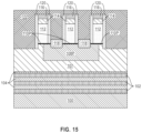
- FIG. 14 is a cross sectional view of the exemplary semiconductor structure of FIG. 13 after forming first dielectric spacers, first source/drain regions, patterning the semiconductor material layer to provide a semiconductor fin, and forming additional dielectric material.
- FIG. 15 is a cross sectional view of the exemplary semiconductor structure of FIG. 14 after forming a first gap fill dielectric material.
- FIG. 16 is a cross sectional view of the exemplary semiconductor structure of FIG. 15 after replacing each first sacrificial gate structure with a first functional gate structure, wherein each first functional gate structure has a first gate length, forming first source/drain contacts, and forming a dielectric bonding layer.
- FIG. 17 is a cross sectional view of the exemplary semiconductor structure of FIG. 16 after wafer flipping and forming a wafer carrier on the dielectric bonding layer.
- FIG. 18 is a cross sectional view of the exemplary semiconductor structure of FIG. 17 after removing the semiconductor substrate and forming second sacrificial gate structures having a second width that is greater than the first width on a physically exposed surface of a topmost surface of the flipped material stack.
- FIG. 19 is a cross sectional view of the exemplary semiconductor structure of FIG. 18 after forming a second dielectric spacer along the sidewall of each second sacrificial gate structure.
- FIG. 20 is a cross sectional view of the exemplary semiconductor structure of FIG. 19 after further device processing forming a nanosheet stack containing alternating nanosheets of sacrificial semiconductor material and semiconductor channel material from the material stack, recessing the nanosheets of sacrificial semiconductor material, forming an inner dielectric spacer, forming second source/drain regions, and forming a second gap fill dielectric material.
- FIG. 21 is a cross sectional view of the exemplary semiconductor structure of FIG. 20 after replacing each second sacrificial gate structure with a second functional gate structure and forming second source/drain contacts.
- FIG. 1 illustrates an exemplary device layout that can be employed in the present application.
- the exemplary device layout includes a functional gate structure, GS, that straddles over a pair of neighboring semiconductor fins, F 1 and F 2 .
- each semiconductor fin, F 1 and F 2 is orientated parallel to each other and the functional gate structure, GS, lies perpendicular and passes over each of the semiconductor fins, F 1 and F 2 .
- cuts X-X, X 1 -X 1 and Y-Y are also be cuts X-X, X 1 -X 1 and Y-Y.
- Cut X-X is along (and through) a lengthwise direction of semiconductor fin, F 1 , cut X 1 -X 1 is located in an area (i.e., a non-active device area) that is located between the semiconductor fins, F 1 and F 2 , and cut Y-Y is along (and through) a lengthwise direction of the functional gate structure, GS. Cuts X-X and X-X 1 are parallel to each other and cut Y-Y is perpendicular to both cuts X-X and X-X 1 .
- FIGS. 2 A, 3 A, 4 A, 5 A, 6 A, 7 A, 8 A, 9 A, 10 A and 11 A are cross sectional views through Y-Y;
- FIGS. 2 B, 3 B, 4 B, 5 B, 6 B, 7 B, 8 B, 9 B, 10 B and 11 B are cross sectional views through X-X;
- FIGS. 2 C, 3 C, 4 C, 5 C, 6 C, 7 C, 8 C, 9 C, 10 C and 11 C are cross sectional views through X 1 -X 1 .
- the process used to form the FinFET described herein below is replaced with another process that provides the nanosheet FET; this another process that provides the nanosheet FET can be the same as the nanosheet process flow described herein below.
- FIGS. 2 A, 2 B and 2 C there are illustrated an exemplary semiconductor structure that can be employed in the present application and through Y-Y, X-X, and X 1 -X 1 , respectively.
- the exemplary structure shown in FIGS. 2 A, 2 B and 2 C includes a material stack, MS 1 , of alternating layers of sacrificial semiconductor material 14 and semiconductor channel material 16 located on a bottom isolation layer 12 that is located on a semiconductor substrate 10 .
- the bottom isolation layer 12 can be omitted, and in such an embodiment, the material stack, MS 1 , can be located on a surface of semiconductor substrate 10 .
- FIG. 1 the material stack, MS 1 , can be located on a surface of semiconductor substrate 10 .
- a trench isolation structure 11 can be located in the semiconductor substrate 10 so as to define an active device area in which the material stack, MS 1 , is formed thereon.
- the active device area is an upper portion of the semiconductor substrate 10 that is laterally surrounded by the trench isolation structure 11 .
- Each layer of semiconductor channel material 16 is a precursor of a nanosheet stack containing vertical stacked and spaced apart semiconductor channel material nanosheets that are used as an active channel material of a nanosheet FET device of the present application.
- the exemplary structure of FIGS. 2 A, 2 B and 2 C further includes a top isolation layer 18 located on the material stack, MS 1 , at least one semiconductor channel material structure 20 (two semiconductor channel material structures are shown by way of one example) located on the top isolation layer 18 , and a sacrificial gate material-containing stack including at least a first sacrificial gate material layer 24 L is located on the top isolation layer 18 and on each semiconductor channel material structure 20 , and laterally adjacent to the material stack, MS 1 .
- the sacrificial gate material-containing stack can also include a sacrificial gate dielectric material layer 22 .
- the sacrificial gate dielectric material layer 22 can be omitted.
- Each semiconductor channel material structure is a precursor of a semiconductor fin that is used as an active channel material of a FinFET device of the present application.
- the sacrificial gate material-containing stack can be located on physically exposed surfaces (i.e., topmost and sidewall surfaces) of each semiconductor channel material structure 20 , on the physical exposed surfaces (topmost and sidewall surfaces) of the top isolation layer 18 , along the sidewall surfaces of the material stack, MS 1 , along the sidewall surfaces of the bottom isolation layer 12 , if the same is present, and on the topmost surface of the trench isolation structure 11 .
- the semiconductor substrate 10 can be composed of one or more semiconductor materials.
- semiconductor materials that can be used to provide the semiconductor substrate 10 include, but are not limited to, silicon (Si), a silicon germanium (SiGe) alloy, a silicon germanium carbide (SiGeC) alloy, germanium (Ge), III/V compound semiconductors or II/VI compound semiconductors.
- the entirety of the semiconductor substrate 10 is composed of one or more semiconductor materials.
- semiconductor substrate 10 can be referred to a bulk semiconductor substrate.
- semiconductor substrate 10 can be composed of a multilayered stack of from bottom to top, a bottom semiconductor material layer, an insulator material layer, and a top semiconductor material layer.
- a semiconductor substrate 10 can be referred to as a semiconductor-on-insulator (SOI) substrate.
- the top and bottom semiconductor material layers can be composed of one of the semiconductor materials mentioned above, and the insulator material layer can be composed of a dielectric material such as, for example, silicon oxide, and/or boron nitride.
- An SOI substrate can be made utilizing processing techniques well known to those skilled in the art.
- a SOI substrate can be formed by a process referred to as a SIMOX (separation by ion implantation of oxygen) in which oxygen ions are implanted into a bulk semiconductor material and then an anneal is performed to convert the implanted oxygen region into an oxide layer.
- the SOI substrate can be formed by a bonding process in which an oxide (an/or boron nitride) layer that is formed on a semiconductor material layer is bonded to a base semiconductor material layer.
- the trench isolation structure 11 can be composed of a trench dielectric material such as, for example, silicon dioxide, silicon nitride, silicon oxynitride, or any suitable combination of those dielectric materials.
- the trench isolation structure 11 can have a topmost surface that is coplanar with a topmost surface of the semiconductor substrate 10 that defines the active device area. In some embodiments, the trench isolation structure 11 can be omitted.
- the trench isolation structure 11 can be formed by first forming a trench into the semiconductor substrate. The trench can be formed by lithography and etching. The trench is then filled with one of the trench dielectric materials mentioned above. An optional planarization process (such as, for example, chemical mechanical polishing (CMP)) and/or densification process can be performed after the trench fill process.
- CMP chemical mechanical polishing
- the bottom isolation layer 12 is composed of a dielectric material such as, for example, silicon dioxide, silicon nitride, silicon oxynitride, or any suitable combination of those dielectric materials. In some embodiments, the bottom isolation layer 12 is omitted from the structure. When present, the bottom isolation layer 12 can have a thickness from 5 nm to 30 nm; although other thicknesses for the bottom isolation layer 12 are contemplated and can be used in the present application as the thickness of the bottom isolation layer 12 .
- a blanket layer of the dielectric material that provides the bottom isolation layer 12 can be formed on the surface of the semiconductor substrate 10 including the trench isolation structure 11 by a deposition process including, but not limited to, chemical vapor deposition (CVD), plasma enhanced chemical vapor deposition (PECVD) or physical vapor deposition (PVD).
- CVD chemical vapor deposition
- PECVD plasma enhanced chemical vapor deposition
- PVD physical vapor deposition
- the blanket layer of dielectric material that provides the bottom isolation layer 12 can then be patterned during a patterning process used to form the material stack, MS 1 .
- the blanket layer of dielectric material that remains after this patterning process is the bottom isolation layer 12 .
- the material stack, MS 1 includes alternating layers of sacrificial semiconductor material 14 and semiconductor channel material 16 .
- Each layer of sacrificial semiconductor material 14 within the material stack, MS 1 can be referred to as a “sacrificial semiconductor material layer”, and each layer of semiconductor channel material 16 can be referred to as a “semiconductor channel material layer”.
- each layer of semiconductor channel material 16 is sandwiched between bottom and top layers of sacrificial semiconductor material 14 .
- the number of layers of semiconductor channel material 16 within the material stack, MS 1 , of this embodiment of the present application can vary so along as there is at least one layer of semiconductor channel material 16 present in the material stack, MS 1 , and that each layer of semiconductor channel material 16 is sandwiched between bottom and top layers of sacrificial semiconductor material 14 ; in this embodiment of the present application, the material stack, MS 1 , includes ‘x’ number of layers of semiconductor channel material 16 (wherein x begins at 1), and x+1 number of layers of sacrificial semiconductor material 14 .
- the illustrated material stack, MS 1 includes three layers of semiconductor channel material 16 , and four layers of sacrificial semiconductor material 14 .
- Each layer of sacrificial semiconductor material 14 is composed of a first semiconductor material, while each layer of semiconductor channel material 16 is composed of a second semiconductor material that is compositionally different from the first semiconductor material.
- the second semiconductor material that provides each layer of semiconductor channel material 16 is a semiconductor material that is capable of providing high channel mobility for n-type FET devices. In other embodiments, the second semiconductor material that provides each layer of semiconductor channel material 16 is a semiconductor material that is capable of providing high channel mobility for p-type FET devices.
- the first semiconductor material that provides each layer of sacrificial semiconductor material 14 and the second semiconductor material that provides each layer of semiconductor channel material 16 can include one of the semiconductor materials mentioned above for semiconductor substrate 10 .
- the first semiconductor material that provides each layer of sacrificial semiconductor material 14 can be compositionally the same as, or compositionally different from, at least an uppermost semiconductor material portion of the semiconductor substrate 10 .
- the first semiconductor material that provides each layer of sacrificial semiconductor material 14 is compositionally different from at least the uppermost semiconductor material portion of the semiconductor substrate 10 .
- the second semiconductor material that provides each layer of semiconductor channel material 16 can be compositionally the same as, or compositionally different from, at least an uppermost semiconductor material portion of the semiconductor substrate 10 .
- the second semiconductor material that provides each layer of semiconductor channel material 16 is compositionally the same as at least the uppermost semiconductor material portion of the semiconductor substrate 10 .
- the semiconductor substrate 10 is composed silicon
- the first semiconductor material that provides each layer of sacrificial semiconductor material 14 is composed of a silicon germanium alloy
- the second semiconductor material that provides each layer of semiconductor channel material 16 is composed of silicon.
- Other combinations of semiconductor materials are possible as long as the first semiconductor material that provides each layer of sacrificial semiconductor material 14 is compositionally different from the second semiconductor material that provides each layer of semiconductor channel material 16 .
- each layer of sacrificial semiconductor material 14 has a width that is the same as a width of each layer of semiconductor channel material 16 .
- the sidewalls of each layer of sacrificial semiconductor material 14 are vertically aligned with the sidewalls of each layer of semiconductor channel material 16 .
- a typical width for each layer of sacrificial semiconductor material 14 and each layer of semiconductor channel material 16 is from 3 nm to 10 nm. Other widths are contemplated and can be used as the widths of each layer of sacrificial semiconductor material 14 and each layer of semiconductor channel material 16 .
- each layer of sacrificial semiconductor material 14 can be the same or different from the thickness of each layer of semiconductor channel material 16 .
- a typical thickness for each layer of sacrificial semiconductor material 14 and each layer of semiconductor channel material 16 is from 3 nm to 15 nm. Other thicknesses are contemplated and can be used as the thickness of each layer of sacrificial semiconductor material 14 and each layer of semiconductor channel material 16 .
- each layer of sacrificial semiconductor material 14 is shown to be the same, the present application contemplates an embodiment in which the bottommost layer of sacrificial semiconductor material 14 that is closest to the semiconductor substrate 10 can be thicker than the remaining layers of sacrificial semiconductor material 14 within the material stack, MS 1 .
- the material stack, MS 1 including the alternating layers of sacrificial semiconductor material 14 and semiconductor channel material 16 can be formed by an epitaxially growth process, followed by a patterning process Notably, alternating layers of the first semiconductor material 14 and the second semiconductor 16 mentioned above are epitaxially grown in alternating fashion to provide alternating layers of the first and second semiconductor materials on atop the bottom isolation layer 12 , if present, or atop the semiconductor substrate 10 including the trench isolation structure 11 .
- the epitaxial grown layers are then patterned by lithography and etching to provide the material stack, MS 1 .
- the patterning process used to form the material stack, MS 1 can also be used to pattern blanket layers that provide the bottom insulator layer 12 and the top insulator layer 16 .
- Epitaxial semiconductor material layers can be grown from gaseous or liquid precursors and may be grown using vapor-phase epitaxy (VPE), molecular-beam epitaxy (MBE), liquid-phase epitaxy (LPE), or other suitable process.
- VPE vapor-phase epitaxy
- MBE molecular-beam epitaxy
- LPE liquid-phase epitaxy
- epitaxial silicon (Si), silicon germanium (SiGe), and/or carbon doped silicon (Si:C) silicon can be doped during deposition (in-situ doped) by adding dopants, n-type dopants (e.g., phosphorus or arsenic) or p-type dopants (e.g., boron or gallium), depending on the type of FET being formed.
- n-type dopants e.g., phosphorus or arsenic
- p-type dopants e.g., boron or gallium
- the top isolation layer 18 is composed of a dielectric material such as, for example, silicon dioxide, silicon nitride, silicon oxynitride, or any suitable combination of those dielectric materials.
- the top isolation layer 18 can be compositionally the same as, or compositionally different from the bottom isolation layer 12 .
- the bottom isolation layer 12 is composed of silicon nitride, while the top isolation layer 18 is composed of silicon dioxide.
- the top isolation layer 18 can have a thickness from 10 nm to 100 nm; although other thicknesses for the top isolation layer 18 are contemplated and can be used in the present application as the thickness of the top isolation layer 18 .
- a blanket layer of the dielectric material that provides the top isolation layer 18 can be formed on the surface of the material stack including the alternating layers of sacrificial semiconductor material and semiconductor channel material by a deposition process including, but not limited to, CVD, PECVD or PVD.
- the blanket layer of dielectric material that provides the top isolation layer 18 can then be patterned during a patterning process used to form the material stack, MS 1 .
- the blanket layer of dielectric material that remains atop the material stack, MS 1 after the patterning process provides the top isolation layer 18 .
- At least one semiconductor channel material structure 20 is then formed on the surface of the top isolation layer 18 . It is noted that although the present application describes and illustrates the formation of two semiconductor channel material structures 20 on the top isolation layer 18 , the present application is not limited to forming that number of semiconductor channel material structures 20 . Instead, the present application contemplates embodiments in which a single semiconductor channel material structure 20 , or more than two semiconductor channel material structures 20 are formed on the top isolation layer 18 .
- Each semiconductor channel material structure 20 is composed of one of the semiconductor materials mentioned above for the semiconductor substrate 10 .
- the semiconductor material that provides each semiconductor channel material structure 20 can be compositionally the same as, or compositionally different from, at least an uppermost semiconductor material of semiconductor substrate 10 .
- Each semiconductor channel material structure 20 that is formed above the material stack, MS 1 is composed of a compositionally same semiconductor material.
- the semiconductor materials that provide each semiconductor channel material structure 20 can be selected to provide high channel mobility for n-type FET devices, or high channel mobility for p-type FET devices.
- Each semiconductor channel material structure 20 is oriented parallel to each other.
- Each semiconductor channel material structure 20 typically has a same height and width.
- each semiconductor channel material structure 20 has a height as measured from a topmost surface of the top isolation layer 18 to the topmost surface of the semiconductor channel material structure 20 , of from 30 nm to 200 nm, and a width, as measured from one sidewall surface of semiconductor channel material structure 20 , to an opposing sidewall surface of the same semiconductor channel material structure, of from 3 nm to 15 nm.
- Other heights and widths besides those mentioned herein are contemplated for the semiconductor channel material structures 20 and can thus be employed in the present application.
- Each semiconductor channel material structures 20 can be formed by deposition of a semiconductor material, followed by a lithography and etching process. The deposition of the semiconductor material can include an epitaxial growth process.
- the sacrificial gate material-containing stack including at least the first sacrificial gate material layer 24 L is then formed on physically exposed surfaces (i.e., topmost and sidewall surfaces) of each semiconductor channel material structure 20 , on the physical exposed surfaces (topmost and sidewall surfaces) of the top isolation layer 18 , along the sidewall surfaces of the material stack, MS 1 , along the sidewall surfaces of the bottom isolation layer 12 , if the same is present, and on the topmost surface of the trench isolation structure 11 .
- a sacrificial gate dielectric material layer 22 can be present beneath the first sacrificial gate material layer 24 L.
- the optional sacrificial gate dielectric material layer 22 can be composed of a sacrificial gate dielectric material such as, for example, silicon dioxide, silicon nitride, and/or silicon oxynitride.
- the optional sacrificial gate dielectric material layer 22 can have a thickness from 1 nm to 15 nm, although other thicknesses are contemplated and can be used as the thickness of the optional sacrificial gate dielectric material layer 22 .
- the first sacrificial gate material layer 24 L can be composed of a first sacrificial gate material including, but not limited to, polysilicon, amorphous silicon, amorphous silicon germanium, tungsten, titanium, tantalum, aluminum, nickel, ruthenium, palladium, platinum, or alloys of such metals.
- a semiconductor material is used as the first sacrificial gate material
- the semiconductor material that provides the first sacrificial gate material layer 24 L is compositionally different from the semiconductor material that provides each semiconductor channel material structure 20 .
- the first sacrificial gate material layer 24 L can have a thickness from 20 nm to 150 nm, although other thicknesses are contemplated and can be used as the thickness of the first sacrificial gate material layer 24 L.
- the sacrificial gate material-containing stack including the sacrificial gate dielectric material layer 22 , if present, and the first sacrificial gate material layer 24 L can be formed by deposition of the various layers that provide the sacrificial gate material-containing stack.
- the sacrificial gate dielectric material layer 22 can be formed by a first deposition process such as, for example, CVD, PECVD, or PVD, and thereafter the first sacrificial gate material layer 24 L can be formed by a second deposition process including, for example, CVD, PECVD, or PVD.
- an epitaxial growth process can be used to form the first sacrificial gate material layer 24 L.
- FIGS. 3 A, 3 B and 3 C there are illustrated the exemplary semiconductor structure shown in FIGS. 2 A, 2 B and 2 C , respectively, after recessing the first sacrificial gate material layer 24 L to provide a recessed first sacrificial gate material layer 24 R.
- the recessing of the first sacrificial gate material layer 24 L can be performed utilizing a recess etching process (such as a reactive ion etch, or a chemical etch) that removes an upper portion of the first sacrificial gate material layer 24 L.
- a recess etching process such as a reactive ion etch, or a chemical etch
- the recessing includes a selective recessing process such as, for example, a reactive ion etch.
- the recessed first sacrificial gate material layer 24 R has a height that is less than a height of a vertical material stack containing, the optional bottom isolation layer 12 , the material stack, MS 1 , and the top isolation layer 18 .
- the first sacrificial material layer 24 L is removed from atop the semiconductor channel material structures 20 and form the area that is located laterally adjacent to the semiconductor channel material structures 20 .
- FIGS. 4 A, 4 B and 4 C there are shown the exemplary semiconductor structure of FIGS. 3 A, 3 B and 3 C , respectively, after forming a second sacrificial gate material layer 26 L on the recessed first sacrificial gate material layer 24 R.
- the sacrificial gate material that provides the second sacrificial gate material 26 L includes one of the sacrificial gate materials mentioned above for the first sacrificial gate material layer 24 L as long as the second sacrificial gate material layer 26 L is composed a sacrificial gate material that is compositionally different from the sacrificial gate material that provides the first sacrificial gate material layer 24 L.
- the second sacrificial gate material layer 26 L is formed atop the semiconductor channel material structures 20 , and in the area that is located laterally adjacent to the semiconductor channel material structure 20 and laterally adjacent to an upper portion of the vertical stack containing the optional bottom isolation layer 12 , the material stack, MS 1 , and the top isolation layer 18 .
- the second sacrificial gate material layer 26 L can be formed utilizing a deposition process such as, for example, CVD, PECVD or PVD.
- a deposition process such as, for example, CVD, PECVD or PVD.
- an epitaxial growth process can be used to form such a layer.
- FIGS. 5 A, 5 B and 5 C there is shown the exemplary semiconductor structure of FIGS. 4 A, 4 B and 4 C , respectively, after patterning the second sacrificial gate material layer 26 L and the recessed first sacrificial gate material layer 24 L to provide a sacrificial gate material-containing pillar 24 P/ 26 P containing a remaining portion of the second sacrificial gate material layer 26 L and a remaining portion of the recessed first sacrificial gate material layer 24 R.
- the remaining portion of the second sacrificial gate material layer 26 L can be referred to herein as a second sacrificial gate material portion 26 P, while the remaining portion of the recessed first sacrificial gate material layer 24 R can be referred to as a first sacrificial gate material portion 24 P.
- the second sacrificial gate material portion 26 and the first sacrificial gate material portion 24 P have sidewalls that are vertically aligned with each other.
- the sacrificial gate material-containing pillar 24 P/ 26 P can be formed by first depositing a hard mask material layer (not shown) on the topmost surface of the second sacrificial gate material layer 26 L.
- the hard mask material layer is composed of a hard mask material such as, for example, silicon nitride or a multilayered stack of silicon nitride and silicon dioxide.
- the hard mask material layer can have a thickness from 20 nm to 100 nm; although other thicknesses for the hard mask material layer are contemplated and can be employed in the present application as the thickness of the hard mask material layer.
- the hard mask material layer is then patterned by lithography and etching to form a hard mask 30 on a portion of the second sacrificial gate material layer 26 L.
- the second sacrificial gate material layer 26 L and the recessed first sacrificial gate material layer 24 R that are not protected by the hard mask 30 are then removed utilizing one or more etching processes.
- the one or more etching processes stop on a topmost surface of sacrificial gate dielectric material layer 22 .
- the one or more etching processes can remove portions of the sacrificial gate dielectric material layer 22 that are not protected by the hard mask 30 .
- the sacrificial gate material-containing pillar 24 P/ 26 P containing hard mask 30 can be referred to herein as a sacrificial gate structure.
- FIGS. 6 A, 6 B and 6 C there are shown the exemplary semiconductor structure of FIGS. 5 A, 5 B and 5 C , respectively, after thinning the recessed first sacrificial gate material layer (i.e., the first sacrificial gate material portion 24 P) to provide a modified sacrificial gate material-containing pillar 24 T/ 26 P containing the remaining portion of the second sacrificial gate material layer (i.e., second sacrificial gate material portion 26 P) and a remaining thinned portion of the recessed first sacrificial gate material layer (i.e., the first sacrificial gate material portion 24 P).
- the remaining thinned portion of the recessed first sacrificial gate material layer (i.e., the first sacrificial gate material portion 24 P) can be referred herein as a trimmed first sacrificial gate material portion 24 T.
- the trimmed first sacrificial gate material portion 24 T has a first width, W 1
- the second sacrificial gate material portion 26 P has a second width, W 2 .
- W 1 is less than W 2 .
- W 1 is from 10 nm to 200 nm, while W 2 is from 12 nm to 200 nm.
- This thinning step includes a trimming process such as, an etch, that is selective in removing the sacrificial gate material that provides the first sacrificial gate material layer 24 L as compared to the sacrificial gate material that provides the second sacrificial gate material layer 26 L.
- the etch includes a chemical wet etching process.
- FIGS. 7 A, 7 B and 7 C there are illustrated the exemplary semiconductor structure of FIGS. 6 A, 6 B and 6 C , respectively, after forming a dielectric spacer 32 along the physically exposed sidewall of the modified sacrificial gate material-containing pillar 24 T/ 26 P. As is shown in FIG.
- a lower portion of the dielectric spacer 32 that is present laterally adjacent to the trimmed first sacrificial gate material portion 24 T has a first thickness W 3
- a middle portion of the dielectric spacer 32 that is present laterally adjacent to the second sacrificial gate material portion 26 P has a second thickness W 4
- an upper portion of the dielectric spacer 32 is located laterally adjacent to the hard mask 30 and this upper portion of the dielectric spacer 32 has W 4 .
- W 3 is greater than W 4 .
- the dielectric spacer 32 is composed of a dielectric spacer material such as, for example, silicon oxide, silicon nitride, or silicon oxynitride. In some embodiments, and as is illustrated in FIGS. 7 B and 7 C , the dielectric spacer 32 is pillar shaped and has a topmost surface that is coplanar with a topmost surface of the hard mask 30 .
- the dielectric spacer 32 can be formed by deposition of the dielectric spacer material, followed by a spacer etch.
- FIGS. 8 A, 8 B and 8 C there are illustrated the exemplary semiconductor structure shown in FIGS. 7 A, 7 B and 7 C , respectively, after further device processing including forming a semiconductor fin 21 from each semiconductor channel material structure 20 and a nanosheet stack containing alternating nanosheets of sacrificial semiconductor material (not shown) and semiconductor channel materials 16 NS from the material stack, MS 1 , forming bottom and top source/drain regions 46 and 50 , respectively, removing the modified sacrificial gate material-containing pillar 24 T/ 24 P and each nanosheet of sacrificial semiconductor material from the nanosheet stack, and forming a first functional gate structure 34 / 36 having a first gate length in an area previously occupied by the recessed nanosheets of sacrificial semiconductor material as well as in the area previously occupied by the remaining thinned portion of the recessed first sacrificial gate material layer 24 R (i.e., trimmed first sacrificial gate material portion 24 T), and forming a second
- the further device processing includes forming at least one semiconductor fin 21 from each semiconductor channel material structure 20 , and a nanosheet stack (not specifically shown) containing alternating nanosheets of sacrificial semiconductor material (not specifically shown) and semiconductor channel material 16 NS from the material stack, MS 1 .
- Each semiconductor fin 21 includes a remaining portion of the semiconductor channel material structure 20 .
- each nanosheet of sacrificial semiconductor material includes a remaining portion of the layer of sacrificial semiconductor material 14
- each nanosheet of semiconductor channel material 16 NS includes a remaining portion of the layer of a semiconductor channel material 16 .
- the alternating nanosheets of sacrificial semiconductor material (not specifically shown) and semiconductor channel material 16 NS that comprise the nanosheet stack have a reduced width as compared to the alternating layers of sacrificial semiconductor material 14 and semiconductor channel material 16 present in material stack, MS 1 .
- the height of the nanosheets of sacrificial semiconductor material (not specifically shown) and semiconductor channel material 16 NS is the same as that of the alternating layers of sacrificial semiconductor material 14 and semiconductor channel material 16 present in material stack, MS 1 .
- the at least one semiconductor fin 21 and the nanosheet stack are formed by removing portions of the semiconductor channel material structure 20 , and portions of the material stack, MS 1 , that are not protected by the hard mask 30 capped sacrificial gate material-containing pillar 24 T/ 26 P and dielectric spacer 32 .
- This removal process includes one or more etching processes.
- this step which includes the one or more etching processes also removes physically exposed portions of the top isolation layer 18 that are not protected the hard mask 30 capped sacrificial gate material-containing pillar 24 T/ 26 P and dielectric spacer 22 .
- the remaining top isolation layer 18 can be referred to as a top isolation structure 18 P.
- the step which includes the one or more etching processes stops on the bottom isolation layer 12 , if present, or if the bottom isolation layer 12 is not present, on the trench isolation structure 11 .
- Each semiconductor fin 21 has a same height as the previous semiconductor channel material structure 20 , and a width that is less than a width of the previous semiconductor channel material structure 20 .
- each nanosheet of sacrificial channel material is recessed utilizing a lateral recess etch process that selectively removes end portions of the nanosheet of sacrificial channel material relative to the nanosheets of semiconductor channel material 16 NS; no recessing of the nanosheets of semiconductor channel material 16 NS occurs.
- a gap is formed at the end of each of the recessed nanosheets sacrificial channel material.
- Inner dielectric spacer 38 is then formed into the gaps.
- Each inner dielectric spacer 38 includes one of the dielectric spacer materials mentioned above for dielectric spacer 32 .
- the dielectric spacer material that provides each inner dielectric spacer 38 can be compositionally the same as, or compositionally different from, the dielectric spacer material that provides the dielectric spacer 32 .
- Each inner dielectric spacer 38 can be formed by deposition of the dielectric spacer material, followed by a spacer etch.
- Each inner dielectric spacer 38 has an outermost sidewall that is vertically aligned to an outermost sidewall of each nanosheet of semiconductor channel material 16 NS.
- a bottom source/drain region 46 is formed.
- a “source/drain” region can be a source region or a drain region depending on subsequent wiring and application of voltages during operation of the FET.
- the bottom source/drain region 46 has a sidewall that is in directly physically contact with the outermost sidewalls of each nanosheet of semiconductor channel material 16 NS.
- the bottom source/drain region 46 comprises a semiconductor material that is composed of a dopant.
- the semiconductor material that provides each bottom source/drain region 46 can include one of the semiconductor materials mentioned above for the semiconductor substrate 10 .
- the semiconductor material that provides the bottom source/drain regions 46 can be compositionally the same, or compositionally different from each nanosheet of semiconductor channel material 16 NS.
- the semiconductor material that provides the bottom source/drain regions 46 is however compositionally different from each recessed sacrificial nanosheet.
- the dopant that is present in each bottom source/drain region 46 can be either a p-type dopant or an n-type dopant.
- p-type refers to the addition of impurities to an intrinsic semiconductor that creates deficiencies of valence electrons.
- examples of p-type dopants, i.e., impurities include, but are not limited to, boron, aluminum, gallium, and indium.
- N-type refers to the addition of impurities that contributes free electrons to an intrinsic semiconductor.
- each bottom source/drain region 46 can have a dopant concentration of from 4 ⁇ 10 20 atoms/cm 3 to 3 ⁇ 10 21 atoms/cm 3 .
- each bottom source/drain region 46 is composed of phosphorus doped silicon.
- Each bottom source/drain region 46 can be formed by an epitaxial growth in which the dopants are present during the epitaxial growth process.
- the bottom source/drain regions 46 grow laterally outward from each of the nanosheets of semiconductor channel material 16 NS.
- a recess etch is then employed so as to remove the bottom source/drain region 46 from being located laterally adjacent both the top isolation structure 18 P and the semiconductor fins 21 .
- a source/drain isolation layer 48 is formed on each bottom source/drain region 46 and laterally adjacent to the top isolation structure 18 P.
- the source/drain isolation layer 48 can include one of the dielectric materials mentioned above for the bottom isolation layer 12 .
- the dielectric material that provides the source/drain isolation layer 48 can be compositionally the same as, or compositionally different from, the dielectric material that provides the bottom isolation layer 12 and/or the top isolation structure 18 P.
- a top source/drain region 50 is then formed on the source/drain isolation layer and laterally adjacent to the semiconductor fins 21 .
- the top source/drain region 50 has a sidewall that is in directly physically contact with the outermost sidewalls of the semiconductor fins 21 ′.
- the top source/drain region 50 comprises a semiconductor material and a dopant that typically has a different conductivity than the dopant present in the bottom source/drain region 46 .
- the semiconductor material that provides each top source/drain region 50 can include one of the semiconductor materials mentioned above for the semiconductor substrate 10 .
- the semiconductor material that provides the top source/drain regions 50 can be compositionally the same, or compositionally different from the semiconductor fins 21 .
- each top source/drain region 50 can be either a p-type dopant or an n-type dopant, as defined above. Again, the dopant present in the top source/drain region 50 typically has a different conductivity than the dopant present in the bottom source/drain region 48 . In one example, each top source/drain region 50 is composed of boron doped silicon.
- Each top source/drain region 50 can be formed by an epitaxial growth in which the dopants are present during the epitaxial growth process.
- the top source/drain region 50 grow laterally on physically exposed surface of the semiconductor fins 21 .
- a recess etch can then be employed so as to remove the top source/drain region 50 from being located above the semiconductor fins 21 .
- the ILD material layer 52 is then formed atop the top source/drain regions 50 and above the semiconductor fins, 21 .
- the ILD material layer 52 can be composed of a dielectric material including, for example, silicon oxide, silicon nitride, undoped silicate glass (USG), fluorosilicate glass (FSG), borophosphosilicate glass (BPSG), a spin-on low-k dielectric layer, a chemical vapor deposition (CVD) low-k dielectric layer or any combination thereof.
- low-k as used throughout the present application denotes a dielectric material that has a dielectric constant of less than silicon dioxide.
- the ILD material layer 52 can include a multilayered structure that includes at least two different dielectric materials stacked one atop the other such as, for example, silicon nitride and silicon dioxide.
- the ILD material layer 52 can be formed by a deposition process such as, for example, CVD, PECVD, or spin-on coating.
- a planarization process can be performed after the deposition of the dielectric material that provides the ILD material layer 52 .
- the planarization process can remove the hard mask cap 30 from the structure.
- the modified sacrificial gate material-containing pillar 24 T/ 26 P is removed from the structure.
- the removal of the modified sacrificial gate material-containing pillar 24 T/ 26 P is performed utilizing one or more etching processes that is selective in removing the modified sacrificial gate material-containing pillar 24 T/ 26 P from the structure.
- the removal of the modified sacrificial gate material-containing pillar 24 T/ 26 P provides a cavity that physically exposed the recessed nanosheets of sacrificial semiconductor material.
- Each recessed nanosheet of sacrificial semiconductor material is then removed utilizing an etching process that selectively removes the semiconductor material that provides the nanosheets of sacrificial semiconductor material relative to the nanosheets of semiconductor channel material 16 NS and the semiconductor fins 21 .
- the selective etch includes vapor HCl.
- each nanosheet semiconductor channel material 16 NS is now vertically stack, spaced apart from each other and suspended above the semiconductor substrate 10 .
- Each nanosheet of semiconductor channel material 16 NS serves as an active channel material of nanosheet FET device, while each semiconductor fin 21 serves as an active channel material of a FinFET device.
- a first (or lower) functional gate structure 34 / 36 having a first gate length, GL 1 is formed in an area previously occupied by the recessed nanosheets of sacrificial semiconductor material and the remaining thinned portion of the recessed first sacrificial gate material layer 24 R (i.e., trimmed first sacrificial gate material portion 24 T).
- the first functional gate structure 34 / 36 is formed around each nanosheet of semiconductor channel material 16 NS.
- the first functional gate structure 34 / 36 includes a first gate dielectric material layer 34 and a first gate electrode 36 .
- the first gate dielectric material layer 34 is composed of a first gate dielectric material.
- the first gate dielectric material that provides the first gate dielectric material layer 34 includes, but is not limited to, silicon oxide, silicon nitride, silicon oxynitride, high-k materials (i.e., dielectric materials having a dielectric constant of greater than 4.0) or any combination of these materials.
- high-k materials include, but are not limited to, metal oxides such as hafnium oxide, hafnium silicon oxide, hafnium silicon oxynitride, lanthanum oxide, lanthanum aluminum oxide, zirconium oxide, zirconium silicon oxide, zirconium silicon oxynitride, tantalum oxide, titanium oxide, barium strontium titanium oxide, barium titanium oxide, strontium titanium oxide, yttrium oxide, aluminum oxide, lead scandium tantalum oxide, and lead zinc niobate.
- the high-k dielectric may further include dopants such as lanthanum, aluminum, magnesium.
- the first gate dielectric material that provides the first gate dielectric material layer 34 can be formed by a deposition process including, but not limited to CVD, PECVD, or atomic layer deposition (ALD).
- the first gate dielectric material layer 34 has a thickness ranging from 1 nm to 5 nm, although less thickness and greater thickness are also envisioned.
- the first gate electrode 36 is composed of a first conductive material.
- the first conductive material that provides the first gate electrode 36 includes, but is not limited to, doped polycrystalline or amorphous silicon, germanium, silicon germanium, a metal (e.g., tungsten (W), titanium (Ti), tantalum (Ta), ruthenium (Ru), hafnium (Hf), zirconium (Zr), cobalt (Co), nickel (Ni), copper (Cu), aluminum (Al), platinum (Pt), tin (Sn), silver (Ag), gold (Au), a conducting metallic compound material (e.g., tantalum nitride (TaN), titanium nitride (TiN), tantalum carbide (TaC), titanium carbide (TiC), titanium aluminum carbide (TiAlC), tungsten silicide (WSi), tungsten nitride (WN), ruthenium oxide (RuO 2 ), cobalt silicide (CoSi
- the first functional gate structure can include a first work function setting layer (not shown) between the first gate dielectric material layer 34 and the gate electrode 36 .
- the first work function setting layer can be composed of a first work function metal (WFM).
- the first WFM can be any suitable material including, but not limited to, a nitride, including but not limited to titanium nitride (TiN), titanium aluminum nitride (TiAlN), hafnium nitride (HfN), hafnium silicon nitride (HfSiN), tantalum nitride (TaN), tantalum silicon nitride (TaSiN), tungsten nitride (WN), molybdenum nitride (MoN), niobium nitride (NbN); a carbide, including but not limited to titanium carbide (TiC) titanium aluminum carbide (TiAlC), tantalum carbide (TaC), haf
- a first conductive material or a combination of multiple first conductive materials can serve as both gate electrode 36 and the first work function setting layer.
- the first gate conductor material and, if present, the first WFM can be formed by any suitable process or any suitable combination of multiple processes, including but not limited to, ALD, CVD, PECVD, PVD, sputtering, or plating.
- the first functional gate structure is formed by depositing a blanket layer of the first gate dielectric material, optionally a blanket layer of the first WFM, and then a layer of the first conductive material is formed.
- a planarization process is then performed to remove the first gate dielectric material, if, present the blanket layer of the first WFM, and the layer of the first conductive material that is formed on a topmost surface of the ILD material layer 52 .
- a recess etch is then used to reduce the height of at least the remaining layer of the first conductive material; the recess etch may also reduce the height of the first WFM.
- the first gate dielectric layer 34 is formed around each of the semiconductor fins 21 , around portions of the top isolation structure 18 P not covered by the semiconductor fins 21 , around each nanosheet of semiconductor channel material 14 NS, and on physically exposed surfaces of the bottom isolation structure 12 and the trench isolation structure 11 .
- the second functional gate structure includes an upper portion of the first gate dielectric material layer 34 , a second gate dielectric material layer 40 , and a second gate electrode 42 .
- a second work function setting layer can be present between the second gate dielectric material layer 40 and the second gate electrode 42 .
- the second gate dielectric material layer 40 includes a second gate dielectric material.
- the second gate dielectric material that provides the second gate dielectric material layer 40 includes one of the first gate dielectric materials mentioned above for the first gate dielectric material layer 34 .
- the second gate dielectric material that provides the second gate dielectric material layer 40 can be compositionally the same as, or compositionally different from, the first gate dielectric material that provides the first gate dielectric material layer 34 .
- the second gate dielectric material that provides the second gate dielectric material layer 40 can be formed using one of the deposition processes mentioned above for forming the first gate dielectric that provides the first gate dielectric material layer 34 .
- the second gate dielectric material layer 40 can have a thickness within thickness range mentioned above for the first gate dielectric material layer 34 .
- the second gate electrode 42 includes a second conductive material.
- the second conductive material that provides the second gate electrode 42 includes one of the first conductive materials mentioned above for the first gate electrode 36 .
- the conductive material that provides the second gate electrode 42 can be compositionally the same as, or compositionally different from, the first conductive material that provides the first gate electrode 42 .
- the second conductive material that provides the second gate electrode can be formed using one of the deposition processes mentioned above for forming the first conductive material that provides the first gate electrode 36 .
- a second work function setting layer that can be optionally present includes a second WFM material.
- the second WFM includes one of the materials mentioned above for the first WFM.
- the second WFM is typically compositionally different from the first WFM.
- the second functional gate structure is formed by depositing a blanket layer of the second gate dielectric material, optionally a blanket layer of the second WFM, and then a layer of the second conductive material is formed. A planarization process is then performed to remove the second gate dielectric material, if, present the blanket layer of the second WFM, and the layer of the second conductive material that is formed on a topmost surface of the ILD material layer 52 .
- the second gate dielectric layer 40 is formed on the first gate dielectric material layer that is formed around each of the semiconductor fins 21 .
- the second gate dielectric layer 40 extends onto a topmost surface of the first gate electrode 36 .
- the second functional gate structure 34 / 40 / 42 that is formed on the semiconductor fins 21 can be referred to as a FinFET
- the first functional gate structure 34 / 36 that is formed in a wrap-around fashion about the vertical nanosheet stack of semiconductor channel material 16 NS can be referred to as a nanosheet FET.
- the nanosheet FET has a gate length that is less than a gate length of the FinFET that is vertically stacked above the nanosheet FET.
- FIGS. 9 A, 9 B, 9 C there is illustrated the exemplary semiconductor structure of FIGS. 5 A, 5 B and 5 C , respectively, after thinning the remaining portion of the second sacrificial gate material layer 26 L (i.e., second sacrificial material portion 26 P) to provide a modified sacrificial gate material-containing pillar 24 P/ 26 T containing the thinned remaining portion of the second sacrificial gate material layer 26 L (i.e., thinned second sacrificial gate material portion 26 T) and the remaining portion of the recessed first sacrificial gate material layer 24 R (i.e., recessed first sacrificial material portion 24 P).
- the second sacrificial gate material layer 26 L i.e., second sacrificial material portion 26 P
- a modified sacrificial gate material-containing pillar 24 P/ 26 T containing the thinned remaining portion of the second sacrificial gate material layer 26 L (i.e.,
- the remaining thinned portion of the second sacrificial gate material layer (i.e., the second sacrificial gate material portion 26 P) can be referred herein as a trimmed second sacrificial gate material portion 26 T.
- the recessed first sacrificial material portion 24 P has first has a first width, W 1
- the trimmed second sacrificial gate material portion 26 T has a second width, W 2 .
- W 1 is greater less than W 2 .
- W 1 is from 12 nm to 200 nm, while W 2 is from 10 nm to 200 nm.
- This thinning step includes a trimming process such as, an etch, that is selective in removing the second sacrificial gate material as compared to the first sacrificial gate material.
- the etch includes a chemical wet etching process.
- Dielectric spacer 32 that is used in this embodiment of the present application includes the same dielectric spacer material as mentioned above for dielectric spacer 32 in the previous embodiment of the present application.
- Dielectric spacer 32 can be formed utilizing the processes techniques mentioned above for forming the dielectric spacer 32 in the previous embodiment of the present application.
- a lower portion of the dielectric spacer 32 that is present laterally adjacent to the sacrificial gate material portion 24 P has a first thickness W 3
- a middle portion of the dielectric spacer 32 that is present laterally adjacent to the trimmed second sacrificial gate material portion 26 T has a second thickness W 4
- an upper portion of the dielectric spacer 32 is located laterally adjacent to the hard mask 30 and has thickness W 4 .
- W 3 is less than W 4 .
- FIGS. 11 A, 11 B and 11 C there are illustrated the exemplary semiconductor structure of FIGS. 10 A, 10 B, and 10 C , respectively, after further device processing including forming a semiconductor fin 21 from each semiconductor channel material structure 20 and a nanosheet stack containing alternating nanosheets of sacrificial semiconductor material (not shown) and semiconductor channel material 16 NS from the material stack, MS 1 , forming bottom and top source/drain regions 46 and 50 , respectively, removing the modified sacrificial gate material-containing pillar 24 P/ 26 T and each nanosheet of sacrificial semiconductor material from the nanosheet stack, and forming a first functional gate structure 34 / 36 having a first gate length, GL 1 , in an area previously occupied by the recessed nanosheets of sacrificial semiconductor material and the remaining portion of the recessed first sacrificial gate material layer 24 L (i.e., the first sacrificial gate material portion 24 P), and forming a second functional gate structure 34 / 40
- FIGS. 8 A, 8 B and 8 C The processing steps and materials mentioned above in forming the exemplary structure shown in FIGS. 8 A, 8 B and 8 C are used here in providing the structure shown in FIGS. 11 A, 11 B and 11 C .
- the second functional gate structure 34 / 40 / 42 that is formed on the semiconductor fins 21 can be referred to as a FinFET
- the first functional gate structure 34 / 36 that is formed in a wrap-around fashion about the vertical nanosheet stack of semiconductor channel material 16 NS can be referred to as a nanosheet FET.
- the nanosheet FET has a gate length that is greater than a gate length of the FinFET that is vertically stacked above the nanosheet FET.
- FIGS. 12 - 21 illustrate another embodiment of the present application.
- a flow over-flow method will be described and illustrated.
- FIG. 12 there is illustrated an exemplary semiconductor structure that can be employed in accordance with this flow over-flow method.
- the exemplary semiconductor structure of FIG. 12 includes a semiconductor substrate 100 , a material stack, MS 2 , of alternating layers of sacrificial semiconductor material 102 and a semiconductor channel material 104 , a first isolation layer 106 , a semiconductor material layer 108 , and a second isolation layer 110 .
- the semiconductor substrate 100 of this embodiment of the present application includes at least one of the semiconductor materials mentioned above for semiconductor substrate 10 .
- the semiconductor substrate 100 can be a bulk semiconductor substrate, as described above in regard to semiconductor substrate 10 .
- the semiconductor substrate 100 can be a semiconductor-on-insulator substrate, as described above in regard to semiconductor substrate 10 .
- the material stack, MS 2 includes alternating layers of sacrificial semiconductor material 102 and semiconductor channel material 104 .
- Each layer of sacrificial semiconductor material 102 within the material stack, MS 2 can be referred to as a “sacrificial semiconductor material layer”, and each layer of semiconductor channel material 104 can be referred to as a “semiconductor channel material layer”.
- the number of layers of semiconductor channel material 104 match the number of layers of sacrificial semiconductor material 102 .
- the number of layers of sacrificial semiconductor material 102 and the number of layers of semiconductor channel material 104 within the material stack, MS 2 can vary.
- the illustrated material stack, MS 2 includes three layers of sacrificial semiconductor material 102 , and three layers of semiconductor channel material 104 .
- Each layer of sacrificial semiconductor material 102 is composed of a first semiconductor material, while each layer of semiconductor channel material 104 is composed of a second semiconductor material that is compositionally different from the first semiconductor material.
- the second semiconductor material that provides each layer of semiconductor channel material 104 is a semiconductor material that is capable of providing high channel mobility for n-type FET devices.
- the second semiconductor material that provides each layer of semiconductor channel material 104 is a semiconductor material that is capable of providing high channel mobility for p-type FET devices.
- the first semiconductor material that provides each layer of sacrificial semiconductor material 102 and the second semiconductor material that provides each layer of semiconductor channel material 104 can include one of the semiconductor materials mentioned above for semiconductor substrate 10 .
- the first semiconductor material that provides each layer of sacrificial semiconductor material 102 can be compositionally the same as, or compositionally different from, at least an uppermost semiconductor material portion of the semiconductor substrate 100 .
- the first semiconductor material that provides each layer of sacrificial semiconductor material 102 is compositionally different from at least the uppermost semiconductor material portion of the semiconductor substrate 100 .
- the second semiconductor material that provides each layer of semiconductor channel material 104 can be compositionally the same as, or compositionally different from, at least an uppermost semiconductor material portion of the semiconductor substrate 100 .
- the second semiconductor material that provides each layer of semiconductor channel material 104 is compositionally the same as at least the uppermost semiconductor material portion of the semiconductor substrate 110 .
- the semiconductor substrate 110 is composed silicon
- the first semiconductor material that provides each layer of sacrificial semiconductor material 102 is composed of a silicon germanium alloy
- the second semiconductor material that provides each layer of semiconductor channel material 104 is composed of silicon.
- Other combinations of semiconductor materials are possible as long as the first semiconductor material that provides each layer of sacrificial semiconductor material 102 is compositionally different from the second semiconductor material that provides each layer of semiconductor channel material 104 .
- each layer of sacrificial semiconductor material 102 can be the same or different from the thickness of each layer of semiconductor channel material 104 .
- a typical thickness for each layer of sacrificial semiconductor material 102 and each layer of semiconductor channel material 104 is from 2 nm to 10 nm. Other thicknesses are contemplated and can be used as the widths of each layer of sacrificial semiconductor material 102 and each layer of semiconductor channel material 104 .
- the material stack, MS 2 including the alternating layers of sacrificial semiconductor material 102 and semiconductor channel material 104 can be formed by an epitaxially growth process
- Epitaxial semiconductor material layers can be grown from gaseous or liquid precursors, and may be grown using vapor-phase epitaxy (VPE), molecular-beam epitaxy (MBE), liquid-phase epitaxy (LPE), or other suitable process.
- VPE vapor-phase epitaxy
- MBE molecular-beam epitaxy
- LPE liquid-phase epitaxy
- epitaxial silicon (Si), silicon germanium (SiGe), and/or carbon doped silicon (Si:C) silicon can be doped during deposition (in-situ doped) by adding dopants, n-type dopants (e.g., phosphorus or arsenic) or p-type dopants (e.g., boron or gallium), depending on the type of FET being formed.
- dopants e.g., phosphorus or arsenic
- p-type dopants e.g., boron or gallium
- the first isolation layer 106 is then formed on the topmost surface of the material stack, MS 2 .
- the first isolation layer 106 is composed of a dielectric material such as, for example, silicon dioxide, silicon nitride, silicon oxynitride, or any suitable combination of those dielectric materials.
- the first isolation layer 106 can have a thickness from 10 nm to 200 nm; although other thickness for the first isolation layer 106 are contemplated and can be used in the present application as the thickness of the first isolation layer 106 .
- the first isolation layer 106 can be formed by a deposition process including, but not limited to, CVD, PECVD or PVD.
- the semiconductor material layer 108 is then formed on the topmost surface of the first isolation layer 106 .
- the semiconductor material layer 108 is composed of one of the semiconductor materials mentioned above for the semiconductor substrate 10 .
- the semiconductor material that provides the semiconductor material layer 108 can be compositionally the same as, or compositionally different from, at least an uppermost semiconductor material of semiconductor substrate 100 .
- the semiconductor material that provides the semiconductor material layer 108 can be selected to provide high channel mobility for n-type FET devices, or high channel mobility for p-type FET devices.
- the semiconductor material layer 108 can have a thickness from 10 nm to 100 nm. Although other thicknesses are contemplated and can be use as the thickness of the semiconductor material layer 108 .
- the semiconductor material layer 108 can be formed by deposition such as, for example, an epitaxial growth process.
- the second isolation layer 110 is then formed on the topmost surface semiconductor material layer 108 .
- the second isolation layer 110 which can be referred to as a sacrificial gate dielectric material layer, is composed one or the dielectric materials mentioned above for the first isolation layer 106 .
- the dielectric material that provides the second isolation layer 110 can be compositionally the same as, or compositionally different from, the dielectric material that provides the first isolation layer 106 .
- the second isolation layer 110 can be formed by a deposition process including, but not limited to, CVD, PECVD or PVD.
- FIG. 13 there is illustrated the exemplary semiconductor structure of FIG. 12 after forming first sacrificial gate structures 112 / 114 / 116 having a first width, W 1 , on a topmost surface of the second isolation layer 110 .
- FIG. 13 illustrates the formation of three first sacrificial gate structures 112 / 114 / 116
- the present application is not limited to that number of first sacrificial gate structures 112 / 114 / 116 .
- the present application contemplates embodiments in which at least one first sacrificial gate structure 112 / 114 / 116 is formed.
- Each first sacrificial gate structure includes at least a sacrificial gate material 112 .
- the sacrificial gate material 112 can be composed one of the first sacrificial gate materials mentioned above for the first sacrificial gate material layer 24 L. That is, sacrificial gate material 112 can include, but is not limited to, polysilicon, amorphous silicon, amorphous silicon germanium, tungsten, titanium, tantalum, aluminum, nickel, ruthenium, palladium, platinum, or alloys of such metals. The thickness of each sacrificial gate material is within the range mentioned above for the first sacrificial gate material layer 24 L.
- Each first sacrificial gate structure can at least one hard mask.
- each first sacrificial gate structure optionally includes a first hard mask 114 and a second hard mask 116 .
- the first hard mask 114 can be composed of a first hard mask material
- the second hard mask 116 can be composed of a second hard mask material that is compositionally different from the first hard mask material.
- the first hard mask 114 is composed of silicon nitride
- the second hard mask 116 can be composed of silicon dioxide.
- Each of the first and second hard masks 114 , 116 can have a thickness from 20 nm to 100 nm; although other thicknesses for the first and second hard masks 114 , 116 are contemplated and can be employed in the present application.
- Each first sacrificial gate structure can be formed by depositing blanket layers of sacrificial gate material and hard mask materials and then the resultant blanket multilayered material stack is patterned by lithography and etching.
- FIG. 14 there is illustrated the exemplary semiconductor structure of FIG. 13 after forming first dielectric spacers 120 , first source/drain regions 118 , patterning the semiconductor material layer 108 to provide a semiconductor fin 108 P, and forming additional dielectric material.
- the first dielectric spacers 120 are formed along a sidewall of each first sacrificial gate structure 112 / 114 / 116 .
- the first dielectric spacers 120 can include one of the dielectric spacer materials mentioned above for dielectric spacer 32 .
- the first dielectric spacers 120 can be formed by depositing the dielectric spacer material, followed by a spacer etch. Each first dielectric spacer 120 can be pillar shaped as is shown in FIG. 14 .
- the physically exposed portions of the second insulator layer 110 are removed utilizing an etching process and the dielectric spacers 120 and the first sacrificial gate structures 112 / 114 / 116 as a combined etch mask.
- the etching process used to remove physically exposed portions of the second insulator layer 110 can include a dry etching process such as, for example, a reactive ion etch.
- the second insulator layer 110 remains under the dielectric spacers 120 and the first sacrificial gate structures 112 / 114 / 116 .
- the remaining second insulator layer 110 can be referred to as a second insulator portion 110 P.
- First source/drain regions 118 are then formed.
- the first source/drain regions 118 include a semiconductor material and a dopant as defined above for the bottom source/drain regions 46 .
- the first source/drain regions 118 can be formed by an epitaxial growth process in which the dopants can be added during the epitaxial growth process or after the epitaxial growth process.
- the first source/drain regions 118 can be formed into a trench that is formed into the semiconductor material layer 108 prior to the epitaxial growth process. In other embodiments, the first source/drain regions 118 can be formed by introducing a p-type or n-type dopant into the semiconductor material layer 108 .
- the semiconduction material layer 108 is then patterned by lithography and etching to provide semiconductor fin 108 P which contains the first source/drain regions 118 .
- the patterning of the semiconduction material layer 108 can occur prior to source/drain formation, yet after forming the first dielectric spacers 120 .
- the additional dielectric material is a same dielectric material as the first insulator layer 106 thus collectively the additional dielectric layer and the first insulator layer 106 provide an insulator structure 107 .
- the additional dielectric material can be formed utilizing one of the deposition processes mentioned above for forming the first insulator layer 106 . In some embodiments, a recess etch can follow the deposition of the additional dielectric material.
- First gap fill dielectric material 122 is composed of a dielectric fill material that is compositionally different from the dielectric materials that provides the first dielectric spacers 120 , the insulator structure 107 , and the topmost hard mask cap of each first sacrificial gate structure.
- the dielectric fill material that provides the first gap fill dielectric material 122 is a silicon nitride based dielectric material such as, for example, silicon nitride, silicon boron carbon nitride, or a dielectric including atoms of Si, O, C and N.
- the dielectric fill material that provides the first gap fill dielectric material 122 is composed of a silicon carbon based dielectric material such as, for example, silicon carbide or a dielectric including atoms of Si, C and O.
- a silicon carbon based dielectric material such as, for example, silicon carbide or a dielectric including atoms of Si, C and O.
- Other dielectric materials besides a silicon nitride based dielectric and a silicon carbon based dielectric material can be used as the dielectric fill material.
- the dielectric fill material can be formed ALD, CVD, PECVD, PVD, evaporation or spin-on coating.
- each first sacrificial gate structure 112 / 114 / 116 with a first functional gate structure 124 / 126 , wherein each first functional gate structure has a first gate length, GL 1 , forming first source/drain contacts 128 , and forming a dielectric bonding layer 130 .
- the replacing each first sacrificial gate structure 112 / 114 / 116 with a first functional gate structure 124 / 126 includes first exposing a topmost surface of each first sacrificial gate structure 112 / 114 / 116 .
- the exposing a topmost surface of each first sacrificial gate structure 112 / 114 / 116 can include a material removal process such as, for example, a planarization process which removes an upper portion of the gap fill dielectric material 122 .
- One or more etching steps are then used to remove each first sacrificial gate structure 112 / 114 / 116 as well as the underlying second insulator structure 110 P.
- the first functional gate structure including at least a first gate dielectric material layer 124 and a first gate electrode 126 .
- An optional first work function setting layer can be formed between the first gate dielectric material layer 124 and a first gate electrode 126 .
- the first gate dielectric material layer 124 includes one of the gate dielectric materials mentioned above for the first gate dielectric material layer 34 .
- the first gate electrode 126 includes one of the conductive materials mentioned above for the first gate electrode 36 .
- the optional first work function setting layer includes one of the previously mentioned first WFMs.
- the first functional gate structure can be formed by first depositing a layer of the first gat dielectric material, an optional layer of the first WFM, and a layer of the conductive material in the area previously occupied by each first sacrificial gate structure 112 / 114 / 116 , and the performing a planarization process to remove any of the layer of the first gat dielectric material, the optional layer of the first WFM, and the layer of the conductive material that is present on the gap fill dielectric material 122 .
- the first source/drain contacts 128 can be formed by forming source/drain contact openings (not shown) in the gap fill dielectric material 122 by lithography and etching, and then filling the contact openings with at least a contact conductor material, as defined herein below.
- a metal semiconductor alloy region can be formed in each of the source/drain contact openings and on an upper surface of the first source/drain regions 118 .
- the metal semiconductor alloy region can be composed of a silicide or germicide.
- the metal semiconductor alloy region can be formed by first depositing a metal layer (not shown) in each of the source/drain contact openings and on an upper surface of the first source/drain regions 118 .
- the metal layer can include a metal such as Ni, Co, Pt, W, Ti, Ta, a rare earth metal (e.g., Er, Yt, La), an alloy thereof, or any combination thereof.
- the metal layer can be deposited by ALD, CVD, PVD or ALD.
- the thickness of the metal layer can be from 2 nm to 10 nm, although lesser and greater thicknesses can also be employed.
- a diffusion barrier (not shown) such as, for example, TiN or TaN, can then be formed over the metal layer.
- An anneal process can be subsequently performed at an elevated temperature to induce reaction of the semiconductor material of the first source/drain regions 118 to provide the metal semiconductor alloy regions.
- the unreacted portion of the metal layer, and, if present, the diffusion barrier then removed, for example, by an etch process (or a plurality of etching processes).
- the etching process can be a wet etch that removes the metal in the metal layer selective to the metal semiconductor alloy in the metal semiconductor alloy regions.
- a source/drain contact material is then deposited in the source/drain contact openings to form the first source/drain contacts 128 .
- the first source/drain contacts 128 can include one or more source/drain contact liners (not shown).
- the contact liner (not shown) can include a diffusion barrier material.
- Exemplary diffusion barrier materials include, but are not limited to, Ti, Ta, Ni, Co, Pt, W, Ru, TiN, TaN, WN, WC, an alloy thereof, or a stack thereof such as Ti/TiN and Ti/WC.
- the contact liner can be formed utilizing a conformal deposition process including CVD or ALD.
- the contact liner that is formed can have a thickness ranging from 1 nm to 5 nm, although lesser and greater thicknesses can also be employed.
- a contact conductor material is subsequently deposited into each of the source/drain contact openings to completely fill a remaining volume of the source/drain contact openings.
- the contact conductor material can include a metal such as, for example, W, Cu, Al, Co, Ru, Mo, Os, Ir, Rh or an alloy thereof.
- the contact conductor layer can be formed by any suitable deposition method such as, for example, ALD, CVD, PVD or plating.
- a planarization process can be used to remove the contact conductor material and the contact liner (when provided) that are located outside the source/drain contact openings. The remaining contact conductor material and if present, the contact liner and the metal semiconductor alloy region provide first source/drain contacts 128 .
- dielectric bonding layer 130 is formed on the gap fill dielectric material 122 and the first functional gate structures 124 / 126 .
- the dielectric bonding layer 130 is composed of a dielectric material such as, for example, silicon dioxide or silicon nitride.
- the dielectric bonding layer 130 can be formed by a deposition process such as, for example, CVD, PECVD, or PVD.
- the dielectric bonding layer 130 can have a thickness from 20 nm to 2000 nm; although thicknesses are contemplated and can be used as the thickness of the dielectric bonding layer 130 .
- FIG. 17 there is illustrated the exemplary semiconductor structure of FIG. 16 after wafer flipping and forming a wafer carrier 132 on the dielectric bonding layer 130 .
- the wafer flipping rotates the exemplary structure shown in FIG. 16 by 1800 such that the semiconductor substrate 100 is now the topmost element of the structure.
- the wafer flipping can be performed manually or utilizing a robotic arm or other wafer flipping apparatus.
- the wafer carrier 132 can include a bulk semiconductor substrate, or a semiconductor-on-insulator substrate, as both defined above for semiconductor substrate 100 . Bonding can be achieved utilizing a thermal bonding process or by adhering the wafer carrier 132 to the dielectric bonding layer 130 .
- FIG. 18 there is illustrated the exemplary semiconductor structure of FIG. 17 after removing the semiconductor substrate 110 and forming second sacrificial gate structures 134 / 136 / 138 / 140 having a second width, W 2 , that is greater than the first width, W 1 , on a physically exposed surface of a topmost surface of the flipped material stack.
- the semiconductor substrate 110 can be removed utilizing a material removal process such as, for example, a planarization (i.e., grinding and/or chemical mechanical polishing).
- the material removal process removes the entirety of the semiconductor substrate 110 and stops on an upper surface of the layer of sacrificial material 102 that previously formed an interface with the semiconductor substrate 110 .
- the second sacrificial gate structures include a second sacrificial gate dielectric material 134 , a second sacrificial gate material 136 , a bottom hard mask cap 138 and a top hard mask cap 140 .
- a single hard mask cap can be employed in the second sacrificial gate structures.
- the second sacrificial gate dielectric material 134 can be omitted from the structure.
- the second sacrificial gate dielectric material 134 can be composed of a sacrificial gate dielectric material such as, for example, silicon dioxide, silicon nitride, and/or silicon oxynitride.
- the second sacrificial gate dielectric material 134 can have a thickness from 1 nm to 15 nm, although other thicknesses are contemplated and can be used as the thickness of the second sacrificial gate dielectric material 134 .
- the second sacrificial gate material 136 can be composed one of the first sacrificial gate material mentioned above for the first sacrificial gate material layer 24 L.
- the bottom hard mask 138 can be composed of a first hard mask material, while the top hard mask 140 can be composed of a second hard mask material that is compositionally different from the first hard mask material.
- the bottom hard mask 138 is composed of silicon nitride, while the top hard mask 140 can be composed of silicon dioxide.
- Each of the bottom and top hard masks 138 , 140 can have a thickness from 20 nm to 100 nm; although other thicknesses for the bottom and top hard masks 138 , 140 are contemplated and can be employed in the present application.
- Each second sacrificial gate structure can be formed by depositing blanket layers of the sacrificial gate dielectric material, the sacrificial gate material and hard mask materials and then the resultant blanket multilayered material stack is patterned by lithography and etching.
- FIG. 19 there is illustrated the exemplary semiconductor structure of FIG. 18 after forming a second dielectric spacer 142 along the sidewall of each second sacrificial gate structure 134 / 1367 / 138 / 140 .
- the second dielectric spacers 142 are formed along a sidewall of each first sacrificial gate structure 134 / 1367 / 138 / 140 .
- the second dielectric spacers 142 can include one of the dielectric spacer materials mentioned above for dielectric spacer 32 .
- the second dielectric spacers 142 can be formed by depositing the dielectric spacer material, followed by a spacer etch. Each second dielectric spacer 142 can be pillar shaped as is shown in FIG. 19 .
- FIG. 20 there is illustrated the exemplary semiconductor structure of FIG. 19 after further device processing including forming at least one nanosheet stack containing alternating nanosheets of sacrificial semiconductor material 102 NS and semiconductor channel material 104 NS from the material stack, recessing the nanosheets of sacrificial semiconductor material 102 NS, forming an inter dielectric spacer 146 , forming second source/drain regions 148 , and forming a second gap fill dielectric material 144 .
- the further device processing includes forming at least one nanosheet stack containing alternating nanosheets of sacrificial semiconductor material 102 NS and semiconductor channel material 104 NS from the material stack, MS 2 .
- Each nanosheet of sacrificial semiconductor material 102 NS includes a remaining portion of the layer of sacrificial semiconductor material 102
- each nanosheet of semiconductor channel material 104 NS includes the layer of a semiconductor channel material 104 .
- the alternating nanosheets of sacrificial semiconductor material 102 NS and semiconductor channel materials 104 NS that comprise the nanosheet stack have a reduced width as compared to the alternating layers of sacrificial semiconductor material 102 and semiconductor channel materials 104 present in material stack, MS 2 .
- the height of the nanosheets of sacrificial semiconductor material 102 NS and semiconductor channel materials 104 NS is the same as that of the alternating layers of sacrificial semiconductor material 102 and semiconductor channel materials 104 present in material stack, MS 2 .
- the at least one nanosheet stack is formed by removing portions of the material stack, MS 2 that are not protected by the second sacrificial gate structure and the second dielectric spacers 142 .
- the removing includes one or more etching processes.
- each nanosheet of sacrificial channel material is recessed utilizing a lateral recess etch process that selectively removes end portions of the nanosheet of sacrificial channel material 102 NS relative to the nanosheets of semiconductor channel material 104 NS; no recessing of the nanosheets of semiconductor channel material 104 NS occurs.
- a gap is formed at the end of each of the recessed nanosheets sacrificial channel material 102 NS.
- Inner dielectric spacer 146 is then formed into the gaps.
- Each inner dielectric spacer 146 includes one of the dielectric spacer materials mentioned above for dielectric spacer 32 .
- the dielectric spacer material that provides each inner dielectric spacer 146 can be compositionally the same as, or compositionally different from, the dielectric spacer material that provides the second dielectric spacer 142 .
- Each inner dielectric spacer 146 can be formed by deposition of the dielectric spacer material, followed by a spacer etch.
- Each inner dielectric spacer 146 has an outermost sidewall that is vertically aligned to an outermost sidewall of each nanosheet of semiconductor channel material 104 NS.
- second source/drain region 148 are formed.
- the second source/drain regions 148 includes a semiconductor material and a dopant as defined above for bottom source/drain regions 46 .
- the second source/drain regions 148 can be formed utilizing the same process as mentioned above for forming the bottom source/drain regions 46 .
- Second gap fill dielectric material 144 includes one of the materials mentioned above for the first gap fill dielectric material 122 .
- the second gate fill dielectric material 144 can be formed utilizing the process mentioned above for forming the first gap fill dielectric material 122 .
- the second gap fill dielectric material 144 is formed laterally adjacent to, and atop each second sacrificial gate structure.
- FIG. 21 there is illustrated the exemplary semiconductor structure of FIG. 20 after replacing each second sacrificial gate structure 134 / 136 / 138 / 140 with a second functional gate structure 150 / 152 and forming second source/drain contacts 154 .
- the replacing second sacrificial gate structure 134 / 136 / 138 / 140 with a second functional gate structure 150 / 152 includes first exposing a second sacrificial gate structure 134 / 136 / 138 / 140 .
- the exposing a topmost surface of each second sacrificial gate structure 134 / 136 / 138 / 140 can include a material removal process such as, for example, a planarization process which removes an upper portion of the second gap fill dielectric material 142 .
- One or more etching steps are then used to remove each second sacrificial gate structure 134 / 136 / 138 / 140 .
- the second functional gate structure including at least a second gate dielectric material layer 150 and a second gate electrode 152 .
- An optional second work function setting layer can be formed between the second gate dielectric material layer 150 and the second gate electrode 152 .
- the second gate dielectric material layer 150 includes one of the gate dielectric materials mentioned above for the first gate dielectric material layer 34 .
- the second gate dielectric material layer 150 can be compositionally the same as, of compositionally different from the first gate dielectric material layer 124 .
- the second gate electrode 150 includes one of the conductive materials mentioned above for the first gate electrode 36 .
- the second gate electrode 150 can be compositionally the same, or compositionally different from, the first gate electrode 126 .
- the optional second work function setting layer includes one of the previously mentioned first WFMs.
- the optional second work function setting layer is typically compositionally different from the optional first work function layer that can be positioned between he first gate dielectric material layer 124 and the first electrode 136 .
- the second functional gate structure can be formed by first depositing a layer of a gate dielectric material, an optional layer of WFM, and a layer of conductive material in the area previously occupied by each second sacrificial gate structure 134 / 136 / 138 / 140 , and the performing a planarization process to remove any of the layer of the gate dielectric material, the optional layer of WFM, and the layer of conductive material that is present on the second gap fill dielectric material 144 .
- the second source/drain contacts 154 include materials mentioned above for the first source/drain contacts 128 .
- the second source/drain contacts 154 can be formed utilizing the technique mentioned above for forming the first source/drain contacts 128 .
- the second source/drain contacts 154 contact a surface of the second source/drain regions 146 .
- the first functional gate structure 124 / 126 that is formed on the semiconductor fin 108 P can be referred to as a FinFET
- the second functional gate structure 150 / 152 that is formed in a wrap-around fashion about the vertical nanosheet stack of semiconductor channel material nanosheets 104 NS can be referred to as a nanosheet FET.
- the nanosheet FET has a gate length that is less than a gate length of the FinFET that is vertically stacked below the nanosheet FET.
- it is possible to provide a structure such as is shown in FIG. 21 in which the gate length of the nanosheet FET is greater than the gate length of the FinFET. This can be done by providing the first sacrificial gate structure with a width that is less than the width of the second sacrificial gate structure.
Landscapes
- Insulated Gate Type Field-Effect Transistor (AREA)
- Chemical & Material Sciences (AREA)
- Engineering & Computer Science (AREA)
- Crystallography & Structural Chemistry (AREA)
- Nanotechnology (AREA)
Abstract
Description
Claims (6)
Priority Applications (2)
| Application Number | Priority Date | Filing Date | Title |
|---|---|---|---|
| US17/411,618 US12107168B2 (en) | 2021-08-25 | 2021-08-25 | Independent gate length tunability for stacked transistors |
| PCT/CN2022/100757 WO2023024681A1 (en) | 2021-08-25 | 2022-06-23 | Independent gate length tunability for stacked transistors |
Applications Claiming Priority (1)
| Application Number | Priority Date | Filing Date | Title |
|---|---|---|---|
| US17/411,618 US12107168B2 (en) | 2021-08-25 | 2021-08-25 | Independent gate length tunability for stacked transistors |
Publications (2)
| Publication Number | Publication Date |
|---|---|
| US20230068484A1 US20230068484A1 (en) | 2023-03-02 |
| US12107168B2 true US12107168B2 (en) | 2024-10-01 |
Family
ID=85287100
Family Applications (1)
| Application Number | Title | Priority Date | Filing Date |
|---|---|---|---|
| US17/411,618 Active 2042-02-23 US12107168B2 (en) | 2021-08-25 | 2021-08-25 | Independent gate length tunability for stacked transistors |
Country Status (2)
| Country | Link |
|---|---|
| US (1) | US12107168B2 (en) |
| WO (1) | WO2023024681A1 (en) |
Families Citing this family (2)
| Publication number | Priority date | Publication date | Assignee | Title |
|---|---|---|---|---|
| US20230290863A1 (en) * | 2022-03-09 | 2023-09-14 | Taiwan Semiconductor Manufacturing Company Limited | Semiconductor device and methods of formation |
| US20250048688A1 (en) * | 2023-07-31 | 2025-02-06 | International Business Machines Corporation | Stacked field effect transistors |
Citations (28)
| Publication number | Priority date | Publication date | Assignee | Title |
|---|---|---|---|---|
| US7026688B2 (en) | 2002-10-01 | 2006-04-11 | Samsung Electronics Co., Ltd. | Field effect transistors having multiple stacked channels |
| US20080061371A1 (en) * | 2004-05-17 | 2008-03-13 | Samsung Electronics Co., Ltd. | Field effect transistor (fet) devices and methods of manufacturing fet devices |
| US7498630B2 (en) | 2003-02-05 | 2009-03-03 | Kabushiki Kaisha Toshiba | Nonvolatile semiconductor memory |
| US20110049624A1 (en) * | 2009-08-26 | 2011-03-03 | International Business Machines Corporation | Mosfet on silicon-on-insulator redx with asymmetric source-drain contacts |
| US20130334610A1 (en) * | 2012-06-13 | 2013-12-19 | Synopsys, Inc. | N-channel and p-channel end-to-end finfet cell architecture with relaxed gate pitch |
| US8802565B2 (en) | 2012-09-10 | 2014-08-12 | International Business Machines Corporation | Semiconductor plural gate lengths |
| US8952438B2 (en) | 2008-09-30 | 2015-02-10 | Samsung Electronics Co., Ltd. | Three-dimensional microelectronic devices including horizontal and vertical patterns |
| US20150279975A1 (en) * | 2014-03-26 | 2015-10-01 | Taiwan Semiconductor Manufacturing Co., Ltd. | Fin sidewall removal to enlarge epitaxial source/drain volume |
| US9184053B2 (en) | 2012-01-10 | 2015-11-10 | Renesas Electronics Corporation | Semiconductor device and method of manufacturing the same |
| US9520330B2 (en) | 2014-12-22 | 2016-12-13 | Commissariat A L'energie Atomique Et Aux Energies Alternatives | Integrated circuit comprising PMOS transistors with different voltage thresholds |
| US20170040315A1 (en) | 2015-08-06 | 2017-02-09 | International Business Machines Corporation | Devices including gates with multiple lengths and methods of manufacturing same |
| US10224329B2 (en) | 2016-04-21 | 2019-03-05 | International Business Machines Corporation | Forming gates with varying length using sidewall image transfer |
| US20190131396A1 (en) | 2017-11-02 | 2019-05-02 | International Business Machines Corporation | Vertically stacked nfets and pfets with gate-all-around structure |
| US20190326286A1 (en) * | 2018-04-20 | 2019-10-24 | Globalfoundries Inc. | Method, apparatus, and system for fin-over-nanosheet complementary field-effect-transistor |
| US20190393249A1 (en) * | 2018-06-22 | 2019-12-26 | Intel Corporation | Stacked thin film transistors |
| US20200006130A1 (en) * | 2018-06-28 | 2020-01-02 | Taiwan Semiconductor Manufacturing Company Ltd. | Semiconductor structure and method for forming the same |
| US20200105869A1 (en) * | 2018-09-28 | 2020-04-02 | International Business Machines Corporation | Formation of dielectric layer as etch-stop for source and drain epitaxy disconnection |
| US20200126987A1 (en) * | 2018-10-22 | 2020-04-23 | International Business Machines Corporation | Interlayer via contacts for monolithic three-dimensional semiconductor integrated circuit devices |
| US10734511B2 (en) * | 2016-03-31 | 2020-08-04 | Intel Corporation | High mobility asymmetric field effect transistors with a band-offset semiconductor drain spacer |
| DE102020102331A1 (en) * | 2011-04-01 | 2020-09-03 | Intel Corporation | STACKED TRANSISTORS WITH DIFFERENT GATE LENGTHS IN DIFFERENT COMPONENT STRATA |
| US20200287046A1 (en) * | 2019-03-05 | 2020-09-10 | International Business Machines Corporation | Integrating nanosheet transistors, on-chip embedded memory, and extended-gate transistors on the same substrate |
| US10832907B2 (en) | 2019-02-15 | 2020-11-10 | International Business Machines Corporation | Gate-all-around field-effect transistor devices having source/drain extension contacts to channel layers for reduced parasitic resistance |
| US10847629B2 (en) | 2017-12-18 | 2020-11-24 | SK Hynix Inc. | Semiconductor device with an oxygen sink and method for fabricating the same |
| US10903315B2 (en) * | 2018-09-28 | 2021-01-26 | International Business Machines Corporation | Formation of dielectric layer as etch-stop for source and drain epitaxy disconnection |
| US10923474B2 (en) | 2018-09-28 | 2021-02-16 | Taiwan Semiconductor Manufacturing Co., Ltd. | Semiconductor structure having gate-all-around devices |
| US20210210349A1 (en) | 2020-01-08 | 2021-07-08 | International Business Machines Corporation | Complementary field-effect transistors |
| US11121044B2 (en) * | 2018-10-10 | 2021-09-14 | International Business Machines Corporation | Vertically stacked nanosheet CMOS transistor |
| US20210407980A1 (en) * | 2020-06-29 | 2021-12-30 | Taiwan Semiconductor Manufacturing Co., Ltd. | 3D Semiconductor Package Including Memory Array |
-
2021
- 2021-08-25 US US17/411,618 patent/US12107168B2/en active Active
-
2022
- 2022-06-23 WO PCT/CN2022/100757 patent/WO2023024681A1/en not_active Ceased
Patent Citations (28)
| Publication number | Priority date | Publication date | Assignee | Title |
|---|---|---|---|---|
| US7026688B2 (en) | 2002-10-01 | 2006-04-11 | Samsung Electronics Co., Ltd. | Field effect transistors having multiple stacked channels |
| US7498630B2 (en) | 2003-02-05 | 2009-03-03 | Kabushiki Kaisha Toshiba | Nonvolatile semiconductor memory |
| US20080061371A1 (en) * | 2004-05-17 | 2008-03-13 | Samsung Electronics Co., Ltd. | Field effect transistor (fet) devices and methods of manufacturing fet devices |
| US8952438B2 (en) | 2008-09-30 | 2015-02-10 | Samsung Electronics Co., Ltd. | Three-dimensional microelectronic devices including horizontal and vertical patterns |
| US20110049624A1 (en) * | 2009-08-26 | 2011-03-03 | International Business Machines Corporation | Mosfet on silicon-on-insulator redx with asymmetric source-drain contacts |
| DE102020102331A1 (en) * | 2011-04-01 | 2020-09-03 | Intel Corporation | STACKED TRANSISTORS WITH DIFFERENT GATE LENGTHS IN DIFFERENT COMPONENT STRATA |
| US9184053B2 (en) | 2012-01-10 | 2015-11-10 | Renesas Electronics Corporation | Semiconductor device and method of manufacturing the same |
| US20130334610A1 (en) * | 2012-06-13 | 2013-12-19 | Synopsys, Inc. | N-channel and p-channel end-to-end finfet cell architecture with relaxed gate pitch |
| US8802565B2 (en) | 2012-09-10 | 2014-08-12 | International Business Machines Corporation | Semiconductor plural gate lengths |
| US20150279975A1 (en) * | 2014-03-26 | 2015-10-01 | Taiwan Semiconductor Manufacturing Co., Ltd. | Fin sidewall removal to enlarge epitaxial source/drain volume |
| US9520330B2 (en) | 2014-12-22 | 2016-12-13 | Commissariat A L'energie Atomique Et Aux Energies Alternatives | Integrated circuit comprising PMOS transistors with different voltage thresholds |
| US20170040315A1 (en) | 2015-08-06 | 2017-02-09 | International Business Machines Corporation | Devices including gates with multiple lengths and methods of manufacturing same |
| US10734511B2 (en) * | 2016-03-31 | 2020-08-04 | Intel Corporation | High mobility asymmetric field effect transistors with a band-offset semiconductor drain spacer |
| US10224329B2 (en) | 2016-04-21 | 2019-03-05 | International Business Machines Corporation | Forming gates with varying length using sidewall image transfer |
| US20190131396A1 (en) | 2017-11-02 | 2019-05-02 | International Business Machines Corporation | Vertically stacked nfets and pfets with gate-all-around structure |
| US10847629B2 (en) | 2017-12-18 | 2020-11-24 | SK Hynix Inc. | Semiconductor device with an oxygen sink and method for fabricating the same |
| US20190326286A1 (en) * | 2018-04-20 | 2019-10-24 | Globalfoundries Inc. | Method, apparatus, and system for fin-over-nanosheet complementary field-effect-transistor |
| US20190393249A1 (en) * | 2018-06-22 | 2019-12-26 | Intel Corporation | Stacked thin film transistors |
| US20200006130A1 (en) * | 2018-06-28 | 2020-01-02 | Taiwan Semiconductor Manufacturing Company Ltd. | Semiconductor structure and method for forming the same |
| US20200105869A1 (en) * | 2018-09-28 | 2020-04-02 | International Business Machines Corporation | Formation of dielectric layer as etch-stop for source and drain epitaxy disconnection |
| US10903315B2 (en) * | 2018-09-28 | 2021-01-26 | International Business Machines Corporation | Formation of dielectric layer as etch-stop for source and drain epitaxy disconnection |
| US10923474B2 (en) | 2018-09-28 | 2021-02-16 | Taiwan Semiconductor Manufacturing Co., Ltd. | Semiconductor structure having gate-all-around devices |
| US11121044B2 (en) * | 2018-10-10 | 2021-09-14 | International Business Machines Corporation | Vertically stacked nanosheet CMOS transistor |
| US20200126987A1 (en) * | 2018-10-22 | 2020-04-23 | International Business Machines Corporation | Interlayer via contacts for monolithic three-dimensional semiconductor integrated circuit devices |
| US10832907B2 (en) | 2019-02-15 | 2020-11-10 | International Business Machines Corporation | Gate-all-around field-effect transistor devices having source/drain extension contacts to channel layers for reduced parasitic resistance |
| US20200287046A1 (en) * | 2019-03-05 | 2020-09-10 | International Business Machines Corporation | Integrating nanosheet transistors, on-chip embedded memory, and extended-gate transistors on the same substrate |
| US20210210349A1 (en) | 2020-01-08 | 2021-07-08 | International Business Machines Corporation | Complementary field-effect transistors |
| US20210407980A1 (en) * | 2020-06-29 | 2021-12-30 | Taiwan Semiconductor Manufacturing Co., Ltd. | 3D Semiconductor Package Including Memory Array |
Non-Patent Citations (3)
| Title |
|---|
| International Search Report dated Aug. 25, 2022, received in a corresponding foreign application, 8 pages. |
| Loubet, N., et al., "Stacked Nanosheet Gate-All-Around Transistor to Enable Scaling Beyond FinFET", 2017 Symposium on VLSI Technology Digest of Technical Papers, Date of Conference:Jun. 5-8, 2017, 2 pages. |
| Wu, S.Y., "Key Technology Enablers of Innovations in the AI and 5G Era", 2019 IEEE International Electron Devices Meeting (IEDM), Date of Conference: Dec. 7-11, 2019, 4 pages. |
Also Published As
| Publication number | Publication date |
|---|---|
| US20230068484A1 (en) | 2023-03-02 |
| WO2023024681A1 (en) | 2023-03-02 |
Similar Documents
| Publication | Publication Date | Title |
|---|---|---|
| US12278237B2 (en) | Stacked FETS with non-shared work function metals | |
| US12513985B2 (en) | CFET with independent gate control and low parasitic capacitance | |
| US12406930B2 (en) | Structure containing a via-to-buried power rail contact structure or a via-to-backside power rail contact structure | |
| US10879180B2 (en) | FinFET with etch-selective spacer and self-aligned contact capping layer | |
| US12154985B2 (en) | Moon-shaped bottom spacer for vertical transport field effect transistor (VTFET) devices | |
| US12426338B2 (en) | Buried power rail with robust connection to a wrap around contact | |
| US12324234B2 (en) | Fork sheet device with better electrostatic control | |
| US20240047524A1 (en) | Stacked nanosheet device with step configuration | |
| WO2023024681A1 (en) | Independent gate length tunability for stacked transistors | |
| WO2024082734A1 (en) | Direct backside self-aligned contact | |
| US12490480B2 (en) | Stacked FETS with contact placeholder structures | |
| US20250311319A1 (en) | Stacked field effect transistors | |
| WO2024099205A1 (en) | Fet dram with backside bitline | |
| US20250192048A1 (en) | Backside dielectric cap | |
| EP4420162B1 (en) | Self-adjusting buried busbar manufacturing for semiconductor components | |
| US12356680B2 (en) | Nanosheet device with air-gaped source/drain regions | |
| US20230042567A1 (en) | Reduced parasitic capacitance semiconductor device containing at least one local interconnect passthrough structure | |
| US20250048688A1 (en) | Stacked field effect transistors | |
| US20250379146A1 (en) | Fork sheet transistors with backside dielectric pillar | |
| US20250380456A1 (en) | Increased backside source/drain contact area and source/drain volume | |
| US20250126838A1 (en) | Co-integration of s/d metal contact cut and wrap-around-contact | |
| US20250081581A1 (en) | Structure with self-aligned offset gate contact and direct backside contact | |
| US20250151345A1 (en) | Module-less nanosheet fets with direct backside contact | |
| US20250107218A1 (en) | Stacked fets containing different shaped inner spacers | |
| US20250293161A1 (en) | Semiconductor device with source/drain contact mol cut structure |
Legal Events
| Date | Code | Title | Description |
|---|---|---|---|
| AS | Assignment |
Owner name: INTERNATIONAL BUSINESS MACHINES CORPORATION, NEW YORK Free format text: ASSIGNMENT OF ASSIGNORS INTEREST;ASSIGNORS:BAO, RUQIANG;WANG, JUNLI;GUO, DECHAO;REEL/FRAME:057286/0740 Effective date: 20210816 |
|
| FEPP | Fee payment procedure |
Free format text: ENTITY STATUS SET TO UNDISCOUNTED (ORIGINAL EVENT CODE: BIG.); ENTITY STATUS OF PATENT OWNER: LARGE ENTITY |
|
| STPP | Information on status: patent application and granting procedure in general |
Free format text: DOCKETED NEW CASE - READY FOR EXAMINATION |
|
| STPP | Information on status: patent application and granting procedure in general |
Free format text: NON FINAL ACTION MAILED |
|
| STPP | Information on status: patent application and granting procedure in general |
Free format text: FINAL REJECTION MAILED |
|
| STPP | Information on status: patent application and granting procedure in general |
Free format text: ADVISORY ACTION MAILED |
|
| STPP | Information on status: patent application and granting procedure in general |
Free format text: DOCKETED NEW CASE - READY FOR EXAMINATION |
|
| STPP | Information on status: patent application and granting procedure in general |
Free format text: NON FINAL ACTION MAILED |
|
| STPP | Information on status: patent application and granting procedure in general |
Free format text: FINAL REJECTION MAILED |
|
| STPP | Information on status: patent application and granting procedure in general |
Free format text: RESPONSE AFTER FINAL ACTION FORWARDED TO EXAMINER |
|
| STPP | Information on status: patent application and granting procedure in general |
Free format text: NOTICE OF ALLOWANCE MAILED -- APPLICATION RECEIVED IN OFFICE OF PUBLICATIONS |
|
| ZAAB | Notice of allowance mailed |
Free format text: ORIGINAL CODE: MN/=. |
|
| STPP | Information on status: patent application and granting procedure in general |
Free format text: PUBLICATIONS -- ISSUE FEE PAYMENT VERIFIED |
|
| STCF | Information on status: patent grant |
Free format text: PATENTED CASE |