US12107159B2 - Semiconductor device - Google Patents
Semiconductor device Download PDFInfo
- Publication number
- US12107159B2 US12107159B2 US17/395,890 US202117395890A US12107159B2 US 12107159 B2 US12107159 B2 US 12107159B2 US 202117395890 A US202117395890 A US 202117395890A US 12107159 B2 US12107159 B2 US 12107159B2
- Authority
- US
- United States
- Prior art keywords
- electrode
- conductive member
- end portion
- semiconductor
- semiconductor region
- Prior art date
- Legal status (The legal status is an assumption and is not a legal conclusion. Google has not performed a legal analysis and makes no representation as to the accuracy of the status listed.)
- Active, expires
Links
Images


Classifications
-
- H01L29/7812—
-
- H—ELECTRICITY
- H10—SEMICONDUCTOR DEVICES; ELECTRIC SOLID-STATE DEVICES NOT OTHERWISE PROVIDED FOR
- H10D—INORGANIC ELECTRIC SEMICONDUCTOR DEVICES
- H10D30/00—Field-effect transistors [FET]
- H10D30/60—Insulated-gate field-effect transistors [IGFET]
- H10D30/64—Double-diffused metal-oxide semiconductor [DMOS] FETs
- H10D30/66—Vertical DMOS [VDMOS] FETs
- H10D30/667—Vertical DMOS [VDMOS] FETs having substrates comprising insulating layers, e.g. SOI-VDMOS transistors
-
- H01L29/0657—
-
- H01L29/165—
-
- H01L29/407—
-
- H01L29/42364—
-
- H01L29/7813—
-
- H—ELECTRICITY
- H10—SEMICONDUCTOR DEVICES; ELECTRIC SOLID-STATE DEVICES NOT OTHERWISE PROVIDED FOR
- H10D—INORGANIC ELECTRIC SEMICONDUCTOR DEVICES
- H10D12/00—Bipolar devices controlled by the field effect, e.g. insulated-gate bipolar transistors [IGBT]
- H10D12/411—Insulated-gate bipolar transistors [IGBT]
- H10D12/441—Vertical IGBTs
- H10D12/461—Vertical IGBTs having non-planar surfaces, e.g. having trenches, recesses or pillars in the surfaces of the emitter, base or collector regions
- H10D12/481—Vertical IGBTs having non-planar surfaces, e.g. having trenches, recesses or pillars in the surfaces of the emitter, base or collector regions having gate structures on slanted surfaces, on vertical surfaces, or in grooves, e.g. trench gate IGBTs
-
- H—ELECTRICITY
- H10—SEMICONDUCTOR DEVICES; ELECTRIC SOLID-STATE DEVICES NOT OTHERWISE PROVIDED FOR
- H10D—INORGANIC ELECTRIC SEMICONDUCTOR DEVICES
- H10D30/00—Field-effect transistors [FET]
- H10D30/60—Insulated-gate field-effect transistors [IGFET]
- H10D30/64—Double-diffused metal-oxide semiconductor [DMOS] FETs
- H10D30/66—Vertical DMOS [VDMOS] FETs
- H10D30/668—Vertical DMOS [VDMOS] FETs having trench gate electrodes, e.g. UMOS transistors
-
- H—ELECTRICITY
- H10—SEMICONDUCTOR DEVICES; ELECTRIC SOLID-STATE DEVICES NOT OTHERWISE PROVIDED FOR
- H10D—INORGANIC ELECTRIC SEMICONDUCTOR DEVICES
- H10D62/00—Semiconductor bodies, or regions thereof, of devices having potential barriers
- H10D62/10—Shapes, relative sizes or dispositions of the regions of the semiconductor bodies; Shapes of the semiconductor bodies
- H10D62/102—Constructional design considerations for preventing surface leakage or controlling electric field concentration
- H10D62/103—Constructional design considerations for preventing surface leakage or controlling electric field concentration for increasing or controlling the breakdown voltage of reverse-biased devices
- H10D62/105—Constructional design considerations for preventing surface leakage or controlling electric field concentration for increasing or controlling the breakdown voltage of reverse-biased devices by having particular doping profiles, shapes or arrangements of PN junctions; by having supplementary regions, e.g. junction termination extension [JTE]
- H10D62/106—Constructional design considerations for preventing surface leakage or controlling electric field concentration for increasing or controlling the breakdown voltage of reverse-biased devices by having particular doping profiles, shapes or arrangements of PN junctions; by having supplementary regions, e.g. junction termination extension [JTE] having supplementary regions doped oppositely to or in rectifying contact with regions of the semiconductor bodies, e.g. guard rings with PN or Schottky junctions
-
- H—ELECTRICITY
- H10—SEMICONDUCTOR DEVICES; ELECTRIC SOLID-STATE DEVICES NOT OTHERWISE PROVIDED FOR
- H10D—INORGANIC ELECTRIC SEMICONDUCTOR DEVICES
- H10D62/00—Semiconductor bodies, or regions thereof, of devices having potential barriers
- H10D62/10—Shapes, relative sizes or dispositions of the regions of the semiconductor bodies; Shapes of the semiconductor bodies
- H10D62/117—Shapes of semiconductor bodies
-
- H—ELECTRICITY
- H10—SEMICONDUCTOR DEVICES; ELECTRIC SOLID-STATE DEVICES NOT OTHERWISE PROVIDED FOR
- H10D—INORGANIC ELECTRIC SEMICONDUCTOR DEVICES
- H10D62/00—Semiconductor bodies, or regions thereof, of devices having potential barriers
- H10D62/80—Semiconductor bodies, or regions thereof, of devices having potential barriers characterised by the materials
- H10D62/82—Heterojunctions
- H10D62/822—Heterojunctions comprising only Group IV materials heterojunctions, e.g. Si/Ge heterojunctions
-
- H—ELECTRICITY
- H10—SEMICONDUCTOR DEVICES; ELECTRIC SOLID-STATE DEVICES NOT OTHERWISE PROVIDED FOR
- H10D—INORGANIC ELECTRIC SEMICONDUCTOR DEVICES
- H10D64/00—Electrodes of devices having potential barriers
- H10D64/111—Field plates
- H10D64/117—Recessed field plates, e.g. trench field plates or buried field plates
-
- H—ELECTRICITY
- H10—SEMICONDUCTOR DEVICES; ELECTRIC SOLID-STATE DEVICES NOT OTHERWISE PROVIDED FOR
- H10D—INORGANIC ELECTRIC SEMICONDUCTOR DEVICES
- H10D64/00—Electrodes of devices having potential barriers
- H10D64/20—Electrodes characterised by their shapes, relative sizes or dispositions
- H10D64/27—Electrodes not carrying the current to be rectified, amplified, oscillated or switched, e.g. gates
- H10D64/311—Gate electrodes for field-effect devices
- H10D64/411—Gate electrodes for field-effect devices for FETs
- H10D64/511—Gate electrodes for field-effect devices for FETs for IGFETs
- H10D64/514—Gate electrodes for field-effect devices for FETs for IGFETs characterised by the insulating layers
-
- H—ELECTRICITY
- H10—SEMICONDUCTOR DEVICES; ELECTRIC SOLID-STATE DEVICES NOT OTHERWISE PROVIDED FOR
- H10D—INORGANIC ELECTRIC SEMICONDUCTOR DEVICES
- H10D64/00—Electrodes of devices having potential barriers
- H10D64/20—Electrodes characterised by their shapes, relative sizes or dispositions
- H10D64/27—Electrodes not carrying the current to be rectified, amplified, oscillated or switched, e.g. gates
- H10D64/311—Gate electrodes for field-effect devices
- H10D64/411—Gate electrodes for field-effect devices for FETs
- H10D64/511—Gate electrodes for field-effect devices for FETs for IGFETs
- H10D64/517—Gate electrodes for field-effect devices for FETs for IGFETs characterised by the conducting layers
- H10D64/518—Gate electrodes for field-effect devices for FETs for IGFETs characterised by the conducting layers characterised by their lengths or sectional shapes
-
- H—ELECTRICITY
- H10—SEMICONDUCTOR DEVICES; ELECTRIC SOLID-STATE DEVICES NOT OTHERWISE PROVIDED FOR
- H10D—INORGANIC ELECTRIC SEMICONDUCTOR DEVICES
- H10D64/00—Electrodes of devices having potential barriers
- H10D64/60—Electrodes characterised by their materials
- H10D64/66—Electrodes having a conductor capacitively coupled to a semiconductor by an insulator, e.g. MIS electrodes
- H10D64/68—Electrodes having a conductor capacitively coupled to a semiconductor by an insulator, e.g. MIS electrodes characterised by the insulator, e.g. by the gate insulator
- H10D64/681—Electrodes having a conductor capacitively coupled to a semiconductor by an insulator, e.g. MIS electrodes characterised by the insulator, e.g. by the gate insulator having a compositional variation, e.g. multilayered
-
- H—ELECTRICITY
- H10—SEMICONDUCTOR DEVICES; ELECTRIC SOLID-STATE DEVICES NOT OTHERWISE PROVIDED FOR
- H10D—INORGANIC ELECTRIC SEMICONDUCTOR DEVICES
- H10D64/00—Electrodes of devices having potential barriers
- H10D64/20—Electrodes characterised by their shapes, relative sizes or dispositions
- H10D64/23—Electrodes carrying the current to be rectified, amplified, oscillated or switched, e.g. sources, drains, anodes or cathodes
- H10D64/251—Source or drain electrodes for field-effect devices
- H10D64/252—Source or drain electrodes for field-effect devices for vertical or pseudo-vertical devices
- H10D64/2527—Source or drain electrodes for field-effect devices for vertical or pseudo-vertical devices for vertical devices wherein the source or drain electrodes are recessed in semiconductor bodies
Definitions
- Embodiments described herein relate generally to a semiconductor device.
- a semiconductor device such as a transistor or the like.
- FIG. 1 is a schematic cross-sectional view illustrating a semiconductor device according to a first embodiment
- FIG. 2 is a schematic cross-sectional view illustrating the semiconductor device according to the first embodiment
- FIG. 3 is a graph illustrating the semiconductor device according to the first embodiment
- FIGS. 4 A and 4 B are graphs illustrating characteristics of the semiconductor device
- FIG. 5 is a graph illustrating the semiconductor device according to the first embodiment.
- FIG. 6 is a schematic cross-sectional view illustrating a semiconductor device according to a second embodiment.
- a semiconductor device includes a first electrode, a second electrode, a third electrode, a first conductive member, a semiconductor member, and a first insulating member.
- a direction from the first electrode toward the second electrode is along a first direction.
- the first conductive member includes a first conductive member end portion and a first conductive member other-end portion.
- the first conductive member end portion is between the first electrode and the first conductive member other-end portion in the first direction.
- a position in the first direction of the first conductive member end portion is between a position in the first direction of the first electrode and a position in the first direction of the third electrode.
- the first conductive member is electrically connected with one of the second electrode or the third electrode or being electrically connectable with the one of the second electrode or the third electrode.
- the semiconductor member includes a first semiconductor region of a first conductivity type, a second semiconductor region of a second conductivity type, and a third semiconductor region of the first conductivity type.
- the first semiconductor region includes a first partial region and a second partial region. The first partial region is between the first electrode and the second electrode in the first direction.
- the second semiconductor region is between the first partial region and the third semiconductor region in the first direction.
- the third semiconductor region is electrically connected with the second electrode. A second direction from a portion of the third electrode toward the second semiconductor region crosses the first direction.
- a direction from an other portion of the third electrode toward a portion of the first partial region is along the second direction.
- a direction from the second partial region toward the first conductive member is along the first direction.
- a direction from the first conductive member toward the first partial region is along the second direction.
- At least a portion of the first insulating member is between the semiconductor member and the third electrode and between the semiconductor member and the first conductive member.
- At least a portion of the first insulating member includes silicon, oxygen, and a first element.
- the first element includes at least one selected from the group consisting of hydrogen, helium, argon, and carbon.
- the first insulating member includes a first position, a second position, and a third position. A direction from the first conductive member end portion toward the first position is along the second direction.
- the first position is between the first electrode and the second position in the first direction.
- the third position is between the first position and the second position in the first direction.
- a third concentration of the first element at the third position is greater than a first concentration of the first element at the first position and greater than a second concentration of the first element at the second position.
- a semiconductor device includes a first electrode, a second electrode, a third electrode, a first conductive member, a semiconductor member, and a first insulating member.
- a direction from the first electrode toward the second electrode is along a first direction.
- the first conductive member includes a first conductive member end portion and a first conductive member other-end portion.
- the first conductive member end portion is between the first electrode and the first conductive member other-end portion in the first direction.
- a position in the first direction of the first conductive member end portion is between a position in the first direction of the first electrode and a position in the first direction of the third electrode.
- the first conductive member is electrically connected with one of the second electrode or the third electrode or being electrically connectable with the one of the second electrode or the third electrode.
- the semiconductor member includes a first semiconductor region of a first conductivity type, a second semiconductor region of a second conductivity type, and a third semiconductor region of the first conductivity type.
- the first semiconductor region includes a first partial region and a second partial region. The first partial region is between the first electrode and the second electrode in the first direction.
- the second semiconductor region is between the first partial region and the third semiconductor region in the first direction.
- the third semiconductor region is electrically connected with the second electrode. A second direction from a portion of the third electrode toward the second semiconductor region crosses the first direction.
- a direction from an other portion of the third electrode toward a portion of the first partial region is along the second direction.
- a direction from the second partial region toward the first conductive member is along the first direction.
- a direction from the first conductive member toward the first partial region is along the second direction.
- the first insulating member includes a first position, a second position, and a third position.
- a direction from the first conductive member end portion toward the first position is along the second direction.
- the first position is between the first electrode and the second position in the first direction.
- the third position is between the first position and the second position in the first direction.
- a third potential at the third position is greater than a first potential at the first position and greater than a second potential at the second position.
- FIGS. 1 and 2 are schematic cross-sectional views illustrating a semiconductor device according to a first embodiment.
- the semiconductor device 110 includes a first electrode 51 , a second electrode 52 , a third electrode 53 , a first conductive member 61 , a semiconductor member 10 , and a first insulating member 41 .
- the direction from the first electrode 51 toward the second electrode 52 is along a first direction.
- the first direction is taken as a Z-axis direction.
- a direction perpendicular to the Z-axis direction is taken as an X-axis direction.
- a direction perpendicular to the Z-axis direction and the X-axis direction is taken as a Y-axis direction.
- the position in the first direction (the Z-axis direction) of the third electrode 53 is between the position in the first direction of the first electrode 51 and the position in the first direction of the second electrode 52 .
- the first conductive member 61 includes a first conductive member end portion 61 a and a first conductive member other-end portion 61 b.
- the first conductive member end portion 61 a and the first conductive member other-end portion 61 b are Z-axis direction end portions.
- the first conductive member end portion 61 a is between the first electrode 51 and the first conductive member other-end portion 61 b in the first direction.
- the first conductive member end portion 61 a is, for example, a lower end portion.
- the position in the first direction of the first conductive member end portion 61 a is between the position in the first direction of the first electrode 51 and the position of the first direction of a third electrode end portion 53 a.
- the third electrode 53 includes a third electrode end portion 53 a and a third electrode other-end portion 53 b.
- the third electrode end portion 53 a and the third electrode other-end portion 53 b are Z-axis direction end portions.
- the third electrode end portion 53 a is between the first electrode 51 and the third electrode other-end portion 53 b in the first direction (the Z-axis direction).
- the third electrode end portion 53 a is the end portion of the third electrode 53 at the first electrode 51 side.
- the third electrode end portion 53 a is, for example, the lower end portion.
- the position in the first direction (the Z-axis direction) of the first conductive member end portion 61 a is between the position in the first direction of the first electrode 51 and the position in the first direction of the third electrode end portion 53 a.
- the position in the first direction of the first conductive member other-end portion 61 b is between the position in the first direction of the first electrode 51 and the position in the first direction of the third electrode other-end portion 53 b.
- the position in the first direction of the first conductive member other-end portion 61 b is between the position in the first direction of the third electrode end portion 53 a and the position in the first direction of the third electrode other-end portion 53 b.
- the first conductive member 61 extends along the Z-axis direction.
- the first conductive member 61 is electrically connected with one of the second electrode 52 or the third electrode 53 . Or, the first conductive member 61 is electrically connectable with one of the second electrode 52 or the third electrode 53 . In the semiconductor device 110 , the first conductive member 61 is electrically connected with the second electrode 52 .
- the first conductive member 61 is electrically connected with the second electrode 52 via a connection member 61 C, a connection member 52 LL, and a connection member 52 C.
- connection members may be located at a position that is different from the cross section illustrated in FIG. 1 .
- a terminal 52 T may be connected with the second electrode 52 via the connection member 52 C.
- a terminal 61 T may be electrically connected with the first conductive member 61 via the connection member 61 C.
- the terminal 61 T may be electrically connected with the terminal 52 T by the connection member 52 LL.
- the connection member 52 LL may be provided separately from the semiconductor device 110 .
- the semiconductor member 10 is between the first electrode 51 and the second electrode 52 .
- the semiconductor member 10 includes, for example, a semiconductor such as silicon, etc.
- the semiconductor member 10 includes a first semiconductor region 11 of a first conductivity type, a second semiconductor region 12 of a second conductivity type, and a third semiconductor region 13 of the first conductivity type. As shown in FIG. 1 , the semiconductor member 10 may further include a fourth semiconductor region 14 . As shown in FIG. 1 , the semiconductor member 10 may further include a fifth semiconductor region 15 .
- the first conductivity type is an n-type; and the second conductivity type is a p-type.
- the first conductivity type may be the p-type; and the second conductivity type may be the n-type.
- the first conductivity type is the n-type; and the second conductivity type is the p-type.
- the first semiconductor region 11 includes a first partial region 11 a and a second partial region 11 b.
- the first partial region 11 a is between the first electrode 51 and the second electrode 52 in the first direction (the Z-axis direction).
- the second semiconductor region 12 is between the first partial region 11 a and the third semiconductor region 13 in the first direction (the Z-axis direction).
- the first partial region 11 a, the second semiconductor region 12 , and the third semiconductor region 13 are between the first electrode 51 and the second electrode 52 .
- the third semiconductor region 13 is electrically connected with the second electrode 52 .
- the second direction is, for example, the X-axis direction.
- the direction from another portion of the third electrode 53 toward a portion of the first partial region 11 a is along the second direction (e.g., the X-axis direction).
- the direction from the second partial region 11 b of the first semiconductor region 11 toward the first conductive member 61 is along the first direction (the Z-axis direction).
- the direction from the first conductive member 61 toward the first partial region 11 a is along the second direction (e.g., the X-axis direction).
- the fourth semiconductor region 14 is located between the first electrode 51 and the first semiconductor region 11 in the first direction (the Z-axis direction).
- the fourth semiconductor region 14 is of the first conductivity type (e.g., the n-type).
- the fourth semiconductor region 14 is electrically connected with the first electrode 51 .
- the fourth semiconductor region 14 may include, for example, a semiconductor substrate.
- the first-conductivity-type carrier concentration in the fourth semiconductor region 14 is greater than the first-conductivity-type carrier concentration in the first semiconductor region 11 .
- the first semiconductor region 11 is, for example, an n-region or an n ⁇ -region.
- the fourth semiconductor region 14 is, for example, an n + -region.
- the first-conductivity-type carrier concentration in the third semiconductor region 13 is greater than the first-conductivity-type carrier concentration in the first semiconductor region 11 .
- the third semiconductor region 13 is, for example, an n + -region.
- the fifth semiconductor region 15 is located between the second semiconductor region 12 and the second electrode 52 .
- the fifth semiconductor region 15 is of the second conductivity type (e.g., the p-type).
- the second-conductivity-type carrier concentration in the fifth semiconductor region 15 is greater than the second-conductivity-type carrier concentration in the second semiconductor region 12 .
- the second semiconductor region 12 is a p-region.
- the fifth semiconductor region 15 is a p + -region.
- the second electrode 52 includes a portion 52 a and a portion 52 b.
- the fifth semiconductor region 15 is between the second semiconductor region 12 and the portion 52 a.
- the third electrode 53 is between the first electrode 51 and the portion 52 b.
- the first insulating member 41 is between the semiconductor member 10 and the third electrode 53 and between the semiconductor member 10 and the first conductive member 61 .
- the first insulating member 41 includes a first insulating region 41 a and a second insulating region 41 b.
- the first insulating region 41 a is between the third electrode 53 and the second semiconductor region 12 in the second direction (e.g., the X-axis direction).
- the second insulating region 41 b is between the first conductive member 61 and the semiconductor member 10 .
- a portion of the first insulating member 41 is between the third electrode 53 and the portion 52 b.
- the current that flows between the first electrode 51 and the second electrode 52 can be controlled by the potential of the third electrode 53 .
- the potential of the third electrode 53 is, for example, a potential that is referenced to the potential of the second electrode 52 .
- the first electrode 51 functions as a drain electrode.
- the second electrode 52 functions as a source electrode.
- the third electrode 53 functions as a gate electrode.
- the first insulating region 41 a functions as a gate insulating film.
- the first conductive member 61 functions as a field plate.
- the semiconductor device 110 is, for example, a transistor.
- the first insulating member 41 includes silicon, oxygen, and a first element.
- the first element includes at least one selected from the group consisting of hydrogen, helium, argon, and carbon.
- the first element is, for example, hydrogen or a proton.
- the first insulating member 41 includes a first position p 1 , a second position p 2 , and a third position p 3 .
- the direction from the first conductive member end portion 61 a toward the first position p 1 is along the second direction (e.g., the X-axis direction).
- the position (e.g., the depth) in the Z-axis direction of the first position p 1 corresponds to the depth of the lower end of the first conductive member 61 .
- the first position p 1 is between the first electrode 51 and the second position p 2 in the first direction (the Z-axis direction).
- the second position p 2 is higher than the first position p 1 .
- the distance along the Z-axis direction between the second position p 2 and the first conductive member other-end portion 61 b is less than the distance along the Z-axis direction between the second position p 2 and the first conductive member end portion 61 a.
- the third position p 3 is between the first position p 1 and the second position p 2 in the first direction (the Z-axis direction). According to the embodiment, the concentration of the first element is different between these positions. The concentration of the first element changes along the Z-axis direction.
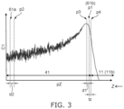
- FIG. 3 is a graph illustrating the semiconductor device according to the first embodiment.
- FIG. 3 illustrates the concentration of the first element (e.g., a proton) of the semiconductor device 110 .
- the horizontal axis of FIG. 3 is a position pZ along the Z-axis direction.
- the position pZ corresponds to the depth.
- the vertical axis is a concentration C 1 of the first element (shown logarithmically).
- the concentration (a first concentration) of the first element at the first position p 1 is greater than the concentration (a second concentration) of the first element at the second position p 2 .
- the concentration (a third concentration) of the first element at the third position p 3 is greater than the first concentration of the first element at the first position p 1 and greater than the second concentration of the first element at the second position p 2 .
- the third concentration is a maximum of the concentration of the first element in the first insulating member 41 .
- the first element can function as a positive charge.
- a high breakdown voltage is obtained by a profile such as that illustrated in FIG. 3 .
- the breakdown voltage can decrease when the concentration (the second concentration) of the first element at a shallow position (e.g., the second position p 2 ) is high.
- a high breakdown voltage can be maintained by reducing the concentration (the second concentration) of the first element at the shallow position (e.g., the second position p 2 ).
- the first-conductivity-type impurity concentration in the first semiconductor region 11 can be set to be high by setting the concentration (the first concentration) of the first element to be high at a deep position (e.g., the first position p 1 ).
- the on-resistance can be reduced thereby.
- a high breakdown voltage is obtained by reducing the concentration of the first element at a position that is shallower than a deep position.
- a low on-resistance is obtained.
- a semiconductor device can be provided in which the characteristics can be improved.
- the profile of the first element illustrated in FIG. 3 is obtained by a method such as ion implantation of the first element into a patterning body that includes the semiconductor member 10 and the first insulating member 41 , etc.
- the first element may be introduced to a portion of the first semiconductor region 11 of the semiconductor member 10 .
- the first insulating member 41 may include a fourth position p 4 .
- the fourth position p 4 is between the first electrode 51 and the first position p 1 in the first direction (the Z-axis direction).
- the concentration (a fourth concentration) of the first element at the fourth position p 4 is less than the concentration (the first concentration) of the first element at the first position p 1 .
- the fourth position p 4 is, for example, the lower end of the first insulating member 41 (the portion that contacts the second partial region 11 b of the first semiconductor region 11 ).
- At least a portion of the second partial region 11 b of the first semiconductor region 11 may include the first element.
- the concentration of the first element in at least a portion of the second partial region 11 b is less than the concentration (the fourth concentration) of the first element at the fourth position p 4 .
- the distance along the first direction (the Z-axis direction) between the first position p 1 and the third position p 3 is taken as a first distance d 1 .
- the distance along the first direction between the second partial region 11 b and the first conductive member end portion 61 a is taken as a distance dz.
- the distance dz corresponds to the thickness of the first insulating member 41 at the position of the lower end (the first conductive member end portion 61 a ) of the first conductive member 61 .
- the first distance d 1 is greater than 0 times and not more than 3 times the distance dz.
- the concentration (the third concentration) of the first element at the third position p 3 is greater than 1 times and not more than 10 times the concentration (the first concentration) of the first element at the first position p 1 .
- the distance along the first direction (the Z-axis direction) between the second position p 2 and the first conductive member other-end portion 61 b is taken as a second distance d 2 .
- the second distance d 2 is equal to the distance dz (the distance along the first direction between the second partial region 11 b and the first conductive member end portion 61 a ).
- the concentration (the first concentration) of the first element at the first position p 1 is not less than 2 times and not more than 100 times the concentration (the second concentration) of the first element at the second position p 2 .
- a high breakdown voltage is obtained by such a profile of the first element.
- a low on-resistance is obtained.
- FIGS. 4 A and 4 B are graphs illustrating characteristics of the semiconductor device.
- the horizontal axis of FIG. 4 A is the position pZ in the Z-axis direction.
- a small position pZ corresponds upward in the Z-axis direction in FIG. 1 .
- the horizontal axis of FIG. 4 B is a thickness ratio Rt 1 .
- the thickness ratio Rt 1 is the ratio (d 1 /dz) of the first distance d 1 to the distance dz.
- the first distance d 1 is the distance along the first direction between the first position p 1 and the third position p 3 .
- the distance dz is the distance along the first direction between the second partial region 11 b and the first conductive member end portion 61 a.
- the first-conductivity-type carrier concentration in the first semiconductor region 11 is set so that the on-resistance RonA is 25 m ⁇ cm 2 .
- the first-conductivity-type carrier concentration in the first semiconductor region 11 is set so that the on-resistance RonA is 26 m ⁇ cm 2 .
- the first-conductivity-type carrier concentration in the first semiconductor region 11 of the second configuration CF 2 is applied to the fifth configuration CF 5 .
- the third concentration (the maximum concentration) and the position (the depth) in the Z-axis direction of the third position p 3 at which the third concentration is obtained are modified so that the on-resistance RonA is 25 m ⁇ cm 2 .
- the first-conductivity-type carrier concentration in the first semiconductor region 11 of the third configuration CF 3 is applied to the sixth configuration CF 6 .
- the third concentration (the maximum concentration) and the position (the depth) in the Z-axis direction of the third position p 3 at which the third concentration is obtained are modified so that the on-resistance RonA is 26 m ⁇ cm 2 .
- the breakdown voltage Vb of the first to third configurations CF 1 to CF 3 show the breakdown voltage Vb of the first to third configurations CF 1 to CF 3 .
- the breakdown voltage Vb of the first configuration is about 111.4 V.
- the breakdown voltage Vb of the second configuration CF 2 is about 102.5 V.
- the breakdown voltage Vb of the third configuration CF 3 is about 112.5 V.
- a high breakdown voltage Vb is obtained when the position pZ of the third position p 3 at which the maximum concentration (the third concentration) is obtained is less (i.e., in FIG. 1 , higher than) than the fourth position p 4 .
- a high breakdown voltage Vb is obtained when the position pZ of the third position p 3 at which the maximum concentration (the third concentration) is obtained is less (i.e., in FIG. 1 , higher) than the first position p 1 .
- the first distance d 1 along the first direction between the first position p 1 and the third position p 3 is favorable for the first distance d 1 along the first direction between the first position p 1 and the third position p 3 to be greater than 0 ⁇ m and not more than 1.2 ⁇ m.
- a high breakdown voltage Vb is obtained when the thickness ratio Rt 1 is positive and is greater than 0 and not more than 3.
- FIG. 5 is a graph illustrating the semiconductor device according to the first embodiment.
- FIG. 5 illustrates the profile of the potential of the semiconductor device.
- the horizontal axis of FIG. 5 is the position pZ along the Z-axis direction.
- the vertical axis is a potential PE 1 .
- the first conductive member 61 is electrically connected with the third electrode 53 via the connection member 61 C, the connection member 52 LL, and a connection member 53 C.
- These connection members may be located at a position that is different from the cross section illustrated in FIG. 6 .
- a terminal 53 T may be connected with the third electrode 53 via the connection member 53 C.
- the terminal 61 T may be electrically connected with the first conductive member 61 via the connection member 61 C.
- the terminal 61 T may be electrically connected with the terminal 53 T by the connection member 52 LL.
- the connection member 52 LL may be provided separately from the semiconductor device 111 .
- the concentration of the first element in the first insulating member 41 has a profile such as that illustrated in FIG. 3 .
- a high breakdown voltage is obtained thereby.
- a low on-resistance is obtained.
- the potential of the first insulating member 41 has a profile such as that illustrated in FIG. 5 .
- a high breakdown voltage is obtained thereby.
- a low on-resistance is obtained.
- the first-conductivity-type carrier concentration in the first semiconductor region 11 is favorable for the first-conductivity-type carrier concentration in the first semiconductor region 11 to be, for example, not less than 1.0 ⁇ 10 15 cm ⁇ 3 and not more than 1.0 ⁇ 10 17 cm ⁇ 3 . It is favorable for the second-conductivity-type carrier concentration in the second semiconductor region 12 to be, for example, not less than 1.0 ⁇ 10 16 cm ⁇ 3 and not more than 1.0 ⁇ 10 18 cm ⁇ 3 . It is favorable for the first-conductivity-type carrier concentration in the third semiconductor region 13 to be, for example, not less than 3.0 ⁇ 10 18 cm ⁇ 3 and not more than 3.0 ⁇ 10 20 cm ⁇ 3 .
- first-conductivity-type carrier concentration in the fourth semiconductor region 14 is favorable for the first-conductivity-type carrier concentration in the fourth semiconductor region 14 to be, for example, not less than 1.0 ⁇ 10 17 cm ⁇ 3 and not more than 3.0 ⁇ 10 20 cm ⁇ 3 . It is favorable for the second-conductivity-type carrier concentration in the fifth semiconductor region 15 to be, for example, not less than 1.0 ⁇ 10 18 cm ⁇ 3 and not more than 3.0 ⁇ 10 20 cm ⁇ 3 .
- the first-conductivity-type impurity concentration in the third semiconductor region 13 is greater than the first-conductivity-type impurity concentration in the first semiconductor region 11 .
- the first-conductivity-type impurity concentration in the fourth semiconductor region 14 is greater than the first-conductivity-type impurity concentration in the first semiconductor region 11 .
- the second-conductivity-type impurity concentration in the fifth semiconductor region 15 is greater than the second-conductivity-type impurity concentration in the second semiconductor region 12 .
- the first-conductivity-type impurity concentration in the first semiconductor region 11 is favorable for the first-conductivity-type impurity concentration in the first semiconductor region 11 to be, for example, not less than 1.0 ⁇ 10 15 cm ⁇ 3 and not more than 1.0 ⁇ 10 17 cm ⁇ 3 . It is favorable for the second-conductivity-type impurity concentration in the second semiconductor region 12 to be, for example, not less than 1.0 ⁇ 10 16 cm ⁇ 3 and not more than 1.0 ⁇ 10 18 cm ⁇ 3 . It is favorable for the first-conductivity-type impurity concentration in the third semiconductor region 13 to be, for example, not less than 3.0 ⁇ 10 18 cm ⁇ 3 and not more than 3.0 ⁇ 10 20 cm ⁇ 3 .
- the first-conductivity-type impurity concentration in the fourth semiconductor region 14 is favorable to be, for example, not less than 1.0 ⁇ 10 17 cm ⁇ 3 and not more than 3.0 ⁇ 10 20 cm ⁇ 3 . It is favorable for the second-conductivity-type impurity concentration in the fifth semiconductor region 15 to be, for example, not less than 1.0 ⁇ 10 18 cm ⁇ 3 and not more than 3.0 ⁇ 10 20 cm ⁇ 3 .
- information that relates to the configurations of the semiconductor regions, etc. is obtained by, for example, electron microscopy, etc.
- Information that relates to the concentrations of the impurities in the semiconductor regions is obtained by, for example, EDX (Energy Dispersive X-ray Spectroscopy), SIMS (Secondary Ion Mass Spectrometry), etc.
- Information that relates to the carrier concentrations in the semiconductor regions is obtained by, for example, SCM (Scanning Capacitance Microscopy), etc.
- the third concentration is, for example, the maximum of the concentration of the first element in the first insulating member 41 on a straight line along the first direction (the Z-axis direction) that passes through the first position pl and the second position p 2 .
- Information that relates to the change of the relative concentration of the first element may be obtained by, for example, photoluminescence analysis, etc.
- Information that relates to the change of the relative concentration of the first element may be obtained using an electron microscope image.
- information that relates to the potential can be obtained by measurements using, for example, SNDP (Scanning nonlinear dielectric potentiometry), EFM (Electrostatic Force Microscope), etc.
- a semiconductor device can be provided in which the characteristics can be improved.
Landscapes
- Electrodes Of Semiconductors (AREA)
- Insulated Gate Type Field-Effect Transistor (AREA)
Abstract
Description
Claims (18)
Applications Claiming Priority (2)
| Application Number | Priority Date | Filing Date | Title |
|---|---|---|---|
| JP2021036912A JP7447038B2 (en) | 2021-03-09 | 2021-03-09 | semiconductor equipment |
| JP2021-036912 | 2021-03-09 |
Publications (2)
| Publication Number | Publication Date |
|---|---|
| US20220293785A1 US20220293785A1 (en) | 2022-09-15 |
| US12107159B2 true US12107159B2 (en) | 2024-10-01 |
Family
ID=83156753
Family Applications (1)
| Application Number | Title | Priority Date | Filing Date |
|---|---|---|---|
| US17/395,890 Active 2042-06-09 US12107159B2 (en) | 2021-03-09 | 2021-08-06 | Semiconductor device |
Country Status (3)
| Country | Link |
|---|---|
| US (1) | US12107159B2 (en) |
| JP (1) | JP7447038B2 (en) |
| CN (1) | CN115050833B (en) |
Citations (9)
| Publication number | Priority date | Publication date | Assignee | Title |
|---|---|---|---|---|
| JP2007194283A (en) | 2006-01-17 | 2007-08-02 | Fuji Electric Holdings Co Ltd | Semiconductor device |
| US8198678B2 (en) | 2009-12-09 | 2012-06-12 | Infineon Technologies Austria Ag | Semiconductor device with improved on-resistance |
| US20160087064A1 (en) | 2014-09-22 | 2016-03-24 | Kabushiki Kaisha Toshiba | Semiconductor device, and method of manufacturing semiconductor device |
| JP2016111253A (en) | 2014-12-09 | 2016-06-20 | 豊田合成株式会社 | Semiconductor device and manufacturing method thereof |
| US20160322489A1 (en) * | 2015-04-30 | 2016-11-03 | Infineon Technologies Austria Ag | Semiconductor Device and Trench Field Plate Field Effect Transistor With a Field Dielectric Including Thermally Grown and Deposited Portions |
| WO2018078775A1 (en) | 2016-10-27 | 2018-05-03 | サンケン電気株式会社 | Semiconductor device |
| US20190097045A1 (en) * | 2017-09-26 | 2019-03-28 | Nxp Usa, Inc. | Field-effect transistor and method therefor |
| US20190280112A1 (en) * | 2018-03-06 | 2019-09-12 | Kabushiki Kaisha Toshiba | Semiconductor device, method for manufacturing the same, power circuit, and computer |
| US20200295150A1 (en) * | 2019-03-14 | 2020-09-17 | Kabushiki Kaisha Toshiba | Semiconductor device |
Family Cites Families (7)
| Publication number | Priority date | Publication date | Assignee | Title |
|---|---|---|---|---|
| US7964913B2 (en) | 2007-01-09 | 2011-06-21 | Maxpower Semiconductor, Inc. | Power MOS transistor incorporating fixed charges that balance the charge in the drift region |
| JP2011091086A (en) * | 2009-10-20 | 2011-05-06 | Mitsubishi Electric Corp | Semiconductor device |
| US8546893B2 (en) | 2010-01-12 | 2013-10-01 | Mohamed N. Darwish | Devices, components and methods combining trench field plates with immobile electrostatic charge |
| JP2012204529A (en) * | 2011-03-24 | 2012-10-22 | Toshiba Corp | Semiconductor device and method of manufacturing the same |
| JP2013069817A (en) * | 2011-09-21 | 2013-04-18 | Toshiba Corp | Semiconductor device |
| US8796761B2 (en) | 2012-03-15 | 2014-08-05 | Infineon Technologies Austria Ag | Semiconductor device including charged structure and methods for manufacturing a semiconductor device |
| JP6666305B2 (en) * | 2017-06-09 | 2020-03-13 | 株式会社東芝 | Semiconductor device and manufacturing method thereof |
-
2021
- 2021-03-09 JP JP2021036912A patent/JP7447038B2/en active Active
- 2021-08-06 US US17/395,890 patent/US12107159B2/en active Active
- 2021-08-19 CN CN202110953890.8A patent/CN115050833B/en active Active
Patent Citations (14)
| Publication number | Priority date | Publication date | Assignee | Title |
|---|---|---|---|---|
| JP2007194283A (en) | 2006-01-17 | 2007-08-02 | Fuji Electric Holdings Co Ltd | Semiconductor device |
| US20070187695A1 (en) | 2006-01-17 | 2007-08-16 | C/O Fuji Electric Holdings Co., Ltd. | Semiconductor device and method of forming the same |
| US8198678B2 (en) | 2009-12-09 | 2012-06-12 | Infineon Technologies Austria Ag | Semiconductor device with improved on-resistance |
| JP2014078741A (en) | 2009-12-09 | 2014-05-01 | Infineon Technologies Austria Ag | Semiconductor device with improved on-resistance value |
| US20160087064A1 (en) | 2014-09-22 | 2016-03-24 | Kabushiki Kaisha Toshiba | Semiconductor device, and method of manufacturing semiconductor device |
| JP2016066641A (en) | 2014-09-22 | 2016-04-28 | 株式会社東芝 | Semiconductor device and manufacturing method of semiconductor device |
| JP2016111253A (en) | 2014-12-09 | 2016-06-20 | 豊田合成株式会社 | Semiconductor device and manufacturing method thereof |
| US9691846B2 (en) | 2014-12-09 | 2017-06-27 | Toyoda Gosei Co., Ltd. | Semiconductor device including an insulating layer which includes negatively charged microcrystal |
| US20160322489A1 (en) * | 2015-04-30 | 2016-11-03 | Infineon Technologies Austria Ag | Semiconductor Device and Trench Field Plate Field Effect Transistor With a Field Dielectric Including Thermally Grown and Deposited Portions |
| WO2018078775A1 (en) | 2016-10-27 | 2018-05-03 | サンケン電気株式会社 | Semiconductor device |
| US20200058778A1 (en) | 2016-10-27 | 2020-02-20 | Sanken Electric Co., Ltd. | Semiconductor device |
| US20190097045A1 (en) * | 2017-09-26 | 2019-03-28 | Nxp Usa, Inc. | Field-effect transistor and method therefor |
| US20190280112A1 (en) * | 2018-03-06 | 2019-09-12 | Kabushiki Kaisha Toshiba | Semiconductor device, method for manufacturing the same, power circuit, and computer |
| US20200295150A1 (en) * | 2019-03-14 | 2020-09-17 | Kabushiki Kaisha Toshiba | Semiconductor device |
Non-Patent Citations (1)
| Title |
|---|
| Eyben, P. et al. "Progress towards a physical contact model for scanning spreading resistance microscopy", Materials Science and Engineering B102, (2003) pp. 132-137. |
Also Published As
| Publication number | Publication date |
|---|---|
| US20220293785A1 (en) | 2022-09-15 |
| CN115050833A (en) | 2022-09-13 |
| CN115050833B (en) | 2025-11-04 |
| JP7447038B2 (en) | 2024-03-11 |
| JP2022137413A (en) | 2022-09-22 |
Similar Documents
| Publication | Publication Date | Title |
|---|---|---|
| US10229988B2 (en) | Adaptive charge balanced edge termination | |
| US9190469B2 (en) | Super junction semiconductor device and method for manufacturing the same | |
| US8227854B2 (en) | Semiconductor device having first and second resurf layers | |
| US10236341B2 (en) | Semiconductor device and method for manufacturing the same | |
| US20130161740A1 (en) | Lateral High-Voltage Transistor with Buried Resurf Layer and Associated Method for Manufacturing the Same | |
| US9548400B2 (en) | Method of controlling breakdown voltage of a diode having a semiconductor body | |
| US10600863B2 (en) | Semiconductor device and method for manufacturing the same | |
| US10243038B1 (en) | Semiconductor device | |
| JP6847887B2 (en) | Semiconductor device | |
| US12027618B2 (en) | Semiconductor device | |
| US11362219B2 (en) | Semiconductor device | |
| US12107159B2 (en) | Semiconductor device | |
| US11462637B2 (en) | Semiconductor device and manufacturing method for the same | |
| US20250212500A1 (en) | Semiconductor device | |
| US20200083320A1 (en) | Semiconductor device | |
| US11777028B2 (en) | Semiconductor device | |
| US11824111B2 (en) | Semiconductor device | |
| CN119968937A (en) | Semiconductor devices | |
| US11837637B2 (en) | Semiconductor device having multiple conductive members | |
| US20210280671A1 (en) | Semiconductor device | |
| US10388780B1 (en) | Semiconductor device | |
| Wen et al. | Characterization and Fabrication of the CFM-JTE for 4H-SiC Power Device with High-Efficiency Protection and Increased JTE Dose Tolerance Window | |
| US20260047160A1 (en) | Planar jfet with enhanced channel control | |
| US20260075888A1 (en) | Semiconductor device | |
| US20190148488A1 (en) | Semiconductor device |
Legal Events
| Date | Code | Title | Description |
|---|---|---|---|
| FEPP | Fee payment procedure |
Free format text: ENTITY STATUS SET TO UNDISCOUNTED (ORIGINAL EVENT CODE: BIG.); ENTITY STATUS OF PATENT OWNER: LARGE ENTITY |
|
| STPP | Information on status: patent application and granting procedure in general |
Free format text: DOCKETED NEW CASE - READY FOR EXAMINATION |
|
| AS | Assignment |
Owner name: TOSHIBA ELECTRONIC DEVICES & STORAGE CORPORATION, JAPAN Free format text: ASSIGNMENT OF ASSIGNORS INTEREST;ASSIGNORS:KOBAYASHI, YUSUKE;INOKUCHI, TOMOAKI;GANGI, HIRO;AND OTHERS;SIGNING DATES FROM 20210914 TO 20210927;REEL/FRAME:058280/0286 Owner name: KABUSHIKI KAISHA TOSHIBA, JAPAN Free format text: ASSIGNMENT OF ASSIGNORS INTEREST;ASSIGNORS:KOBAYASHI, YUSUKE;INOKUCHI, TOMOAKI;GANGI, HIRO;AND OTHERS;SIGNING DATES FROM 20210914 TO 20210927;REEL/FRAME:058280/0286 |
|
| STPP | Information on status: patent application and granting procedure in general |
Free format text: NON FINAL ACTION MAILED |
|
| STPP | Information on status: patent application and granting procedure in general |
Free format text: RESPONSE TO NON-FINAL OFFICE ACTION ENTERED AND FORWARDED TO EXAMINER |
|
| STPP | Information on status: patent application and granting procedure in general |
Free format text: NOTICE OF ALLOWANCE MAILED -- APPLICATION RECEIVED IN OFFICE OF PUBLICATIONS |
|
| ZAAA | Notice of allowance and fees due |
Free format text: ORIGINAL CODE: NOA |
|
| ZAAB | Notice of allowance mailed |
Free format text: ORIGINAL CODE: MN/=. |
|
| STPP | Information on status: patent application and granting procedure in general |
Free format text: PUBLICATIONS -- ISSUE FEE PAYMENT VERIFIED |
|
| STCF | Information on status: patent grant |
Free format text: PATENTED CASE |