US12100910B2 - Shape-memory alloy lock for connectors - Google Patents
Shape-memory alloy lock for connectors Download PDFInfo
- Publication number
- US12100910B2 US12100910B2 US17/457,737 US202117457737A US12100910B2 US 12100910 B2 US12100910 B2 US 12100910B2 US 202117457737 A US202117457737 A US 202117457737A US 12100910 B2 US12100910 B2 US 12100910B2
- Authority
- US
- United States
- Prior art keywords
- outer shell
- inner wafer
- wafer
- connector
- shape
- Prior art date
- Legal status (The legal status is an assumption and is not a legal conclusion. Google has not performed a legal analysis and makes no representation as to the accuracy of the status listed.)
- Active
Links
Images


Classifications
-
- H—ELECTRICITY
- H01—ELECTRIC ELEMENTS
- H01R—ELECTRICALLY-CONDUCTIVE CONNECTIONS; STRUCTURAL ASSOCIATIONS OF A PLURALITY OF MUTUALLY-INSULATED ELECTRICAL CONNECTING ELEMENTS; COUPLING DEVICES; CURRENT COLLECTORS
- H01R12/00—Structural associations of a plurality of mutually-insulated electrical connecting elements, specially adapted for printed circuits, e.g. printed circuit boards [PCB], flat or ribbon cables, or like generally planar structures, e.g. terminal strips, terminal blocks; Coupling devices specially adapted for printed circuits, flat or ribbon cables, or like generally planar structures; Terminals specially adapted for contact with, or insertion into, printed circuits, flat or ribbon cables, or like generally planar structures
- H01R12/70—Coupling devices
- H01R12/7005—Guiding, mounting, polarizing or locking means; Extractors
- H01R12/7011—Locking or fixing a connector to a PCB
- H01R12/7052—Locking or fixing a connector to a PCB characterised by the locating members
-
- H—ELECTRICITY
- H01—ELECTRIC ELEMENTS
- H01R—ELECTRICALLY-CONDUCTIVE CONNECTIONS; STRUCTURAL ASSOCIATIONS OF A PLURALITY OF MUTUALLY-INSULATED ELECTRICAL CONNECTING ELEMENTS; COUPLING DEVICES; CURRENT COLLECTORS
- H01R13/00—Details of coupling devices of the kinds covered by groups H01R12/70 or H01R24/00 - H01R33/00
- H01R13/46—Bases; Cases
- H01R13/516—Means for holding or embracing insulating body, e.g. casing, hoods
-
- H—ELECTRICITY
- H01—ELECTRIC ELEMENTS
- H01R—ELECTRICALLY-CONDUCTIVE CONNECTIONS; STRUCTURAL ASSOCIATIONS OF A PLURALITY OF MUTUALLY-INSULATED ELECTRICAL CONNECTING ELEMENTS; COUPLING DEVICES; CURRENT COLLECTORS
- H01R43/00—Apparatus or processes specially adapted for manufacturing, assembling, maintaining, or repairing of line connectors or current collectors or for joining electric conductors
- H01R43/02—Apparatus or processes specially adapted for manufacturing, assembling, maintaining, or repairing of line connectors or current collectors or for joining electric conductors for soldered or welded connections
- H01R43/0256—Apparatus or processes specially adapted for manufacturing, assembling, maintaining, or repairing of line connectors or current collectors or for joining electric conductors for soldered or welded connections for soldering or welding connectors to a printed circuit board
-
- F—MECHANICAL ENGINEERING; LIGHTING; HEATING; WEAPONS; BLASTING
- F16—ENGINEERING ELEMENTS AND UNITS; GENERAL MEASURES FOR PRODUCING AND MAINTAINING EFFECTIVE FUNCTIONING OF MACHINES OR INSTALLATIONS; THERMAL INSULATION IN GENERAL
- F16B—DEVICES FOR FASTENING OR SECURING CONSTRUCTIONAL ELEMENTS OR MACHINE PARTS TOGETHER, e.g. NAILS, BOLTS, CIRCLIPS, CLAMPS, CLIPS OR WEDGES; JOINTS OR JOINTING
- F16B2200/00—Constructional details of connections not covered for in other groups of this subclass
- F16B2200/77—Use of a shape-memory material
-
- H—ELECTRICITY
- H01—ELECTRIC ELEMENTS
- H01R—ELECTRICALLY-CONDUCTIVE CONNECTIONS; STRUCTURAL ASSOCIATIONS OF A PLURALITY OF MUTUALLY-INSULATED ELECTRICAL CONNECTING ELEMENTS; COUPLING DEVICES; CURRENT COLLECTORS
- H01R12/00—Structural associations of a plurality of mutually-insulated electrical connecting elements, specially adapted for printed circuits, e.g. printed circuit boards [PCB], flat or ribbon cables, or like generally planar structures, e.g. terminal strips, terminal blocks; Coupling devices specially adapted for printed circuits, flat or ribbon cables, or like generally planar structures; Terminals specially adapted for contact with, or insertion into, printed circuits, flat or ribbon cables, or like generally planar structures
- H01R12/50—Fixed connections
- H01R12/51—Fixed connections for rigid printed circuits or like structures
- H01R12/55—Fixed connections for rigid printed circuits or like structures characterised by the terminals
- H01R12/57—Fixed connections for rigid printed circuits or like structures characterised by the terminals surface mounting terminals
Definitions
- This disclosure relates generally to connectors and in particular, to utilizing a shape-memory alloy to lock an outer shell to an inner wafer of a connector.
- An on-the-substrate (OTS) connector system typically includes an OTS receptacle cable assembly for electrically connecting to an OTS surface-mount technology (SMT) plug positioned on a substrate, where the substrate electrically connects to a socket on a printed circuit board assembly (PCBA). Subsequent to electrically coupling the OTS receptacle cable assembly to the OTS SMT plug, a substrate underfill adhesive is utilized to bond the OTS connector to the substrate.
- the OTS receptacle cable assembly includes an inner wafer positioned within an outer shell and plastic, where plastic clip notches provide an interference between the inner wafer and the outer shell.
- the OTS receptacle cable assembly is typically manufactured by a vendor and shipped to a manufacturer for assembly, where the plastic clip notches are designed to hold the inner wafer to the outer shell during handling.
- One aspect of an embodiment of the present invention discloses an apparatus comprising an electrical connector with an outer shell and an inner wafer, wherein the inner wafer is configured to slide into a cavity of the outer shell.
- the apparatus further comprises a first end of a shape-memory alloy coupled to a void in the outer shell and configured to interfere with an area on the inner wafer.
- an apparatus comprising an on-the-substrate (OTS) connector with an outer shell and an inner wafer, wherein the inner wafer is configured to slide into a cavity of the outer shell.
- the apparatus further comprises a plurality of surface-mount technology (SMT) leads of the inner wafer configured to mount onto a plurality of landing pads on a printed circuit board assembly (PCBA).
- SMT surface-mount technology
- PCBA printed circuit board assembly
- the apparatus further comprises a first end of a shape-memory alloy coupled to a void in the outer shell and configured to interfere with the inner wafer preventing movement of the inner wafer within the outer shell of OTS connector.
- Another aspect of an embodiment of the present invention discloses a method comprising applying heat to a shape-memory alloy.
- the method further comprises machining the shape-memory alloy based on dimensions and shape of an outer shell and an inner wafer of a connector.
- the method further comprises attaching a first end of the shape-memory alloy to a void in a cavity of the outer shell.
- the method further comprises inserting the inner wafer into the cavity of the outer shell to form the connector.
- the method further comprises actuating the shape-memory alloy to mechanically engage with a corresponding location on the inner wafer of the connector.
- FIG. 1 A depicts a front view of a disassembled on-the-substrate (OTS) connector with outer shell and inner wafer, in accordance with an embodiment of the present invention.
- OTS on-the-substrate
- FIG. 1 B depicts a front view of an assembled on-the-substrate (OTS) connector with outer shell and inner wafer, in accordance with an embodiment of the present invention.
- OTS on-the-substrate
- FIG. 2 depicts a front view of an assembled on-the-substrate (OTS) connector with shape-memory alloy retaining clips positioned under the inner wafer prior to reflow, in accordance with an embodiment of the present invention.
- OTS on-the-substrate
- FIG. 3 depicts a front view of an assembled on-the-substrate (OTS) connector with shape-memory alloy retaining clips positioned under the inner wafer subsequent to reflow, in accordance with an embodiment of the present invention.
- OTS on-the-substrate
- FIG. 4 A depicts an enhanced front view of a single shape-memory alloy retaining clip positioned under the inner wafer prior to reflow, in accordance with an embodiment of the present invention.
- FIG. 4 B depicts an enhanced front view of a single shape-memory alloy retaining clip positioned under the inner wafer subsequent to reflow, in accordance with an embodiment of the present invention.
- FIG. 5 A depicts an enhanced front view of a single shape-memory alloy retaining clip positioned within the inner wafer prior to reflow, in accordance with an embodiment of the present invention.
- FIG. 5 B depicts an enhanced cutaway side view of a single shape-memory alloy retaining clip positioned within the inner wafer prior to reflow, in accordance with an embodiment of the present invention.
- FIG. 6 A depicts an enhanced front view of a single shape-memory alloy retaining clip positioned within the inner wafer subsequent to reflow, in accordance with an embodiment of the present invention.
- FIG. 6 B depicts an enhanced cutaway side view of a single shape-memory alloy retaining clip positioned within the inner wafer subsequent to reflow, in accordance with an embodiment of the present invention.
- FIG. 7 depicts a process for assembling and mounting an on-the-substrate (OTS) connector with shape-memory alloy retaining clips onto a printed circuit board assembly (PCBA), in accordance with an embodiment of the present invention.
- OTS on-the-substrate
- PCBA printed circuit board assembly
- Embodiments of the present invention provide an on-the-substrate (OTS) connector with a shape-memory alloy retaining clips to couple an outer shell to an inner wafer.
- the inner wafer is positioned within the outer shell such that surface-mount technology (SMT) leads of the inner wafer contact corresponding solder paste covered landing pads on a printed circuit board assembly (PCBA) during an attachment process.
- SMT surface-mount technology
- PCBA printed circuit board assembly
- the SMT leads of the inner wafer protrude in a manner to define a seating plane of the OTS connector.
- OTS connectors are often assembled by a vendor and subsequently shipped and/or handled to an assembly site, where a position of the outer shell relative to the inner wafer can shift.
- plastic retaining clips are utilized to provide an interference between the outer shell and the inner wafer of the OTS connector to prevent any shifting.
- an amount of interference is too little, the inner wafer can shift within the outer shell and adversely affect the seating plane of the OTS connector. If an amount of interference is too great, a force required to seat the outer shell post reflow of the PCBA can potentially damage the inner wafer and/or break the plastic retailing clips.
- Embodiments of the present invention provide memory metal retaining clips for securing the outer shell to the inner wafer of the OTS connector, eliminating plastic deformation to the outer shell.
- the memory metal retaining clips secure the outer shell to the inner wafer at a specific distance as to not impede the seating plane of the SMT leads.
- a process for assembling and mounting an on-the-substrate (OTS) connector with shape-memory alloy retaining clips include providing an outer shell and inner wafer for an OTS connector and selecting a memory metal, such as, Nitinol with memory material properties in the 90° C. to 110° C. range.
- the process includes applying heat to the memory metal and machining the memory metal to a shape for providing an interference (i.e., lock) between the outer shell and the inner wafer.
- the process includes attaching the machined memory metal at a location on the outer shell to engage with the inner wafer.
- the process includes actuating the memory metal to mechanically engage with a corresponding location on the inner wafer of the formed OTS connector.
- the OTS connector is positioned on a surface of the PCBA and during a reflow process, the memory metal releases (i.e., disengages) the inner wafer from the outer shell.
- the outer shell is pressed towards the laminate surfaces and an encapsulant/underfill is applied to the PCBA.
- direct contact means that a first element, such as a first structure, and a second element, such as a second structure, are connected without any intermediary conducting, insulating or semiconductor layers at the interface of the two elements.
- substantially, or substantially similar refer to instances in which the difference in length, height, or orientation convey no practical difference between the definite recitation (e.g. the phrase sans the substantially similar term), and the substantially similar variations.
- substantial (and its derivatives) denote a difference by a generally accepted engineering or manufacturing tolerance for similar devices, up to, for example, 10% deviation in value or 10° deviation in angle.
- FIG. 1 A depicts a front view of a disassembled on-the-substrate (OTS) connector with outer shell and inner wafer, in accordance with an embodiment of the present invention.
- OTS connector 100 includes outer shell 102 and inner wafer 104 , with multiple SMT leads 106 for placement on corresponding landing pads on a surface of a PCBA.
- Inner wafer 104 slides into a cavity of outer shell 102 located at a rear area of outer shell 102 , where the cavity of outer shell 102 is defined by length 108 and width 110 .
- a memory metal Prior to sliding inner wafer 104 into outer shell 102 , a memory metal is selected for locking inner wafer 104 within the cavity of outer shell 102 .
- outer shell 102 and inner wafer 104 are associated with OTS connector 100 and serve only as an example embodiment.
- the invention described herein is applicable to any connector that includes at least outer shell 102 and a component insertable and attachable to outer shell 102 .
- FIG. 1 B depicts a front view of an assembled on-the-substrate (OTS) connector with outer shell and inner wafer, in accordance with an embodiment of the present invention.
- OTS on-the-substrate
- the memory metal retaining clips secure outer shell 102 to inner wafer 104 at a specific distance as to not impede the seating plane of SMT leads 106 , therefore ensuring that SMT leads 106 contact corresponding landing pads upon being placed into a desired position on the PCBA.
- FIG. 2 depicts a front view of an assembled on-the-substrate (OTS) connector with shape-memory alloy retaining clips positioned under the inner wafer prior to reflow, in accordance with an embodiment of the present invention.
- OTS connector 100 includes four memory metal retaining clips 202 A, 202 B, 202 C, and 202 D for securing inner wafer 104 to outer shell 102 .
- an amount of memory retaining clips 202 for securing inner wafer to outer shell 102 is dependent on a design of OTS connector 100 and an expected amount of force experienced by OTS connector 100 during a shipping and/or handling process.
- Memory metal retaining clips 202 A, 202 B, 202 C, and 202 D are each in an engaged position preventing movement of inner wafer 104 within outer shell 102 .
- each of memory metal retaining clips 202 A, 202 B, 202 C, and 202 D are positioned in a respective void 204 A, 204 B, 204 C, and 204 D in a cavity of outer shell 102 , where interference between inner wafer 104 and each of memory metal retaining clips 202 A, 202 B, 202 C, and 202 D prevents the movement of inner wafer 104 within outer shell 102 .
- each of memory metal retaining clips 202 A, 202 B, 202 C, and 202 D are actuated to mechanically engage with a respective location on inner wafer 104 .
- each of memory metal retaining clips 202 A, 202 B, 202 C, and 202 D protrude from a respective void 204 A, 204 B, 204 C, and 204 D, perpendicular to a movement of inner wafer 104 within outer shell 102 .
- each of memory metal retaining clips 202 A, 202 B, 202 C, and 202 D prevents a sliding motion of inner wafer 104 within outer shell 102 during a shipping and/or handling process of OTS connector 100 .
- FIG. 3 depicts a front view of an assembled on-the-substrate (OTS) connector with shape-memory alloy retaining clips positioned under the inner wafer subsequent to reflow, in accordance with an embodiment of the present invention.
- OTS connector 100 includes four memory metal retaining clips 202 A, 202 B, 202 C, and 202 D for securing inner wafer 104 to outer shell 102 .
- Memory metal retaining clips 202 A, 202 B, 202 C, and 202 D are each in a disengaged position subsequent to a reflow solder process for the PCBA on which OTS connector 100 is installed.
- each of memory metal retaining clips 202 A, 202 B, 202 C, and 202 D are positioned in a respective void 204 A, 204 B, 204 C, and 204 D in a cavity of outer shell 102 , where no interference is present between inner wafer 104 and each of memory metal retaining clips 202 A, 202 B, 202 C, and 202 D.
- inner wafer 104 is released from outer shell 102 during the reflow solder process and subsequent to cooling of the PCBA, outer shell 102 is pressed to the laminate surface of the PCBA.
- an encapsulant/underfill is applied to the surface of the PCBA with OTS connector 100 .
- FIG. 4 A depicts an enhanced front view of a single shape-memory alloy retaining clip positioned under the inner wafer prior to reflow, in accordance with an embodiment of the present invention.
- the enhanced view of memory metal retaining clip 202 A within void 204 A illustrates a single corner of outer shell 102 and inner wafer 104 .
- Interference plane 402 represents a clearance line between inner wafer 104 and memory metal retaining clip 202 A attached to outer shell 102 in void 204 A.
- Interference plane 402 is parallel to a sliding direction of inner wafer 104 within outer shell 102 .
- memory metal retaining clip 202 A In an engaged position prior to reflow, memory metal retaining clip 202 A is engaged and crosses interference plane 402 , thus preventing any movement of inner wafer 104 within outer shell 102 .
- a first end of memory metal retaining clip 202 A is attached to a surface within void 204 A and a second end of memory metal retaining clip 202 A is not attached to any surface.
- Inner wafer 104 includes an area into which memory metal retaining clip 202 A can actuate into upon crossing interference plane 402 .
- FIG. 4 B depicts an enhanced front view of a single shape-memory alloy retaining clip positioned under the inner wafer subsequent to reflow, in accordance with an embodiment of the present invention.
- this embodiment illustrates a single corner of outer shell 102 and inner wafer 104 with memory metal retaining clip 202 A positioned within void 204 A.
- interference plane 402 represents a clearance line between inner wafer 104 and memory metal retaining clip 202 A attached to outer shell 102 in void 204 A.
- memory metal retaining clip 202 A does not cross interference plane 402 , thus allowing for movement of outer shell 102 from inner wafer 104 .
- a first end of memory metal retaining clip 202 A is attached to a surface within void 204 A and a second end of memory metal retaining clip 202 A is not attached to any surface. It is to be noted, dimension and shape of each memory metal retaining clip is dependent on dimensions and shape of outer shell 102 and inner wafer 104 of OTS connector 100 .
- FIG. 5 A depicts an enhanced front view of a single shape-memory alloy retaining clip positioned within the inner wafer prior to reflow, in accordance with an embodiment of the present invention.
- the enhanced view of memory metal arm 502 attached to outer shell 102 within void 504 illustrates a single corner of outer shell 102 and inner wafer 104 .
- Interference plane 506 represents a clearance line between inner wafer 104 and memory metal arm 502 attached to outer shell 102 in void 504 . In the engaged position, memory metal arm 502 is positioned across the interference plane 506 prior to reflow, thus preventing movement of inner wafer 104 within outer shell 102 .
- a first end of memory metal arm 502 is attached to a surface within void 504 and a second end of memory metal arm 502 is not attached to any surface and free to move upon actuation with applied heat.
- memory metal arm 502 is actuated and mechanical engages with a corresponding area on inner wafer 104 .
- Inner wafer 104 includes a corresponding area where memory metal arm 502 latches onto upon crossing interference plane 502 .
- Memory metal arm 502 is positioned within an area of outer shell 102 and inner wafer 104 , such that memory metal arm 502 engages with an edge of inner wafer 104 .
- the position of memory metal arm 502 is such that minimal or no redesigning of either outer shell 102 or inner wafer 104 is necessary to accommodate memory metal arm 502 .
- FIG. 5 B depicts an enhanced cutaway side view of a single shape-memory alloy retaining clip positioned within the inner wafer prior to reflow, in accordance with an embodiment of the present invention.
- the enhanced cutaway side view of the embodiment discussed in FIG. 5 A illustrates outer shell 102 and inner wafer 104 , where memory metal arm 502 is in an engaged position. In the engaged position, a portion of memory metal arm 502 crossed interference plane 506 , thus preventing inner wafer 104 from sliding within outer shell 102 perpendicular to interference plane 506 .
- a memory metal arm is placeable at each corner of outer shell 102 for interfering with inner wafer 104 , similar to the embodiment discussed with regards to FIG. 2 .
- FIG. 6 A depicts an enhanced front view of a single shape-memory alloy retaining clip positioned within the inner wafer subsequent to reflow, in accordance with an embodiment of the present invention.
- memory metal arm 502 In a disengaged position subsequent to reflow, memory metal arm 502 is retracted and does not cross interference plane 506 , thus allowing for movement of inner wafer 104 within outer shell 102 .
- the movement of outer shell 102 relative to inner wafer 104 allows for outer shell 102 to be pressed to the laminate surface of the PCBA subsequent to reflow and cooling.
- FIG. 6 B depicts an enhanced cutaway side view of a single shape-memory alloy retaining clip positioned within the inner wafer subsequent to reflow, in accordance with an embodiment of the present invention.
- the enhanced cutaway side view of the embodiment discussed in FIG. 6 A illustrates outer shell 102 and inner wafer 104 , where memory metal arm 502 is retracted and in a disengaged position. In the disengaged position, no portion of memory metal arm 502 crossed interference plane 506 , thus allowing for outer shell 102 to slide independently from inner wafer 104 , perpendicular to interference plane 506 .
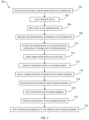
- FIG. 7 depicts a process for assembling and mounting an on-the-substrate (OTS) connector with shape-memory alloy retaining clips onto a printed circuit board assembly (PCBA), in accordance with an embodiment of the present invention.
- OTS on-the-substrate
- PCBA printed circuit board assembly
- the process includes providing an outer shell and inner wafer of a connector ( 702 ).
- the process includes providing an outer shell and an inner wafer of an OTS connector, where the inner wafer slides into the outer shell.
- the outer shell housing the inner wafer form the OTS connector and to prevent movement of the inner wafer within the outer shell, memory metal retaining clips are utilized to provide an interference between the outer shell and the inner wafer.
- the process further includes selecting a memory metal ( 704 ).
- Examples of memory metals i.e., shape-memory alloys
- Nitinol is selected as the memory metal due to a shape transition temperature being in the 90° C. to 110° C. range.
- the shape transition temperature represents the temperature at which a deformed memory metal returns to a pre-deformed shape when heat is applied.
- the process further includes applying heat to the memory metal ( 706 ) and machining the memory metal according to the connector ( 708 ).
- the memory metal is heated to the shape transition temperature utilizing one or more thermal methods that includes baking, handheld heating apparatus, laser, induction, and radiant heat.
- the memory metal (Nitinol) is heated to a value in the 90° C. to 110° C. range and the memory metal is machined to form the memory metal retaining clip.
- Dimensions and a shape of the memory metal retaining clip machined from the memory metal are based on dimensions and shape of the outer shell and the inner wafer of the OTS connector.
- the process further includes attaching the memory metal at a location on the outer shell to engage with the inner wafer ( 710 ).
- Attaching the memory metal at a location on the outer shell can include utilizing mounting methods including but not limited to heat staking, adhesives, and mechanical molding features.
- multiple memory metal retaining clips are attached at multiple voids within the outer shell to engage with multiple areas on the inner wafer, where engagement of the multiple memory metal retaining clips secures outer shell to inside wafer. In a disengaged position, each of the multiple memory metal retaining clip is not actuated and does not cross an interference plane between the outer shell and the inner wafer, thus allowing for movement of inner wafer within outer shell.
- a first end of memory metal retaining clip is attached to a surface within the void and a second end of the memory metal retaining is not attached to any surface and free to move upon actuation with applied heat.
- the process further includes inserting the inner wafer into the outer shell ( 712 ) and engaging the memory metal to the inner wafer ( 714 ).
- Each of the memory metal retaining clips attached to the outer shell mechanically engage with a corresponding location on the inner wafer to secure the inner wafer to the outer shell to form the OTS connector by one or more means.
- the process further includes installing the connector onto a printed circuit board assembly ( 716 ).
- the OTS connector Prior to installing the OTS connector onto the PCBA, the OTS connector is typically shipped from a vendor that manufactured the OTS connector to a manufacturing facility producing the PCBA on which the OTS connector is to be mounted. Since the memory metal retain clips have been actuated, the outer shell interferes with the inner wafer and prevents any movement of the inner wafer relative to the outer shell. As a result, a seating plane of multiple SMT leads of the inner wafer is maintained during the shipping and handling portion of the assembling and mounting process.
- Installing the OTS connector onto the PCBA includes aligning the multiple SMT leads of the inner wafer with corresponding landing pads on the PCBA, where each landing pad include solder paste for subsequently electrically and mechanically coupling the multiple SMT leads of the inner wafer.
- the process further includes reflow soldering the connector onto the printed circuit board assembly ( 718 ).
- the solder paste between each landing pad and each of the multiple SMT leads of the inner wafer reflows in a molten state, creating a permanent solder joint between the landing pads and the multiple SMT leads of the inner wafer.
- each of the multiple memory metal retaining clips retract back behind the interference plane and the inner wafer is released from the outer shell of the OTS connector.
- the process further includes cooling the printed circuit board assembly ( 720 ) and pressing the outer shell to the laminate surface ( 722 ). Since the reflow of the PCBA caused each of the multiple memory metal retaining clips to retract back behind the interference plane, the inner wafer is free to independently move from the outer shell. However, since the multiple SMT leads of the inner wafer were solder to the landing pads, the inner wafer remains fixed to the PCBA. As result, applying a force to the outer shell, results in the outer shell being pushed to the laminated surface of the PCBA.
- the process further includes applying encapsulate/underfill to the printed circuit board assembly ( 724 ). The encapsulant/underfill bonds the OTS connector to the substrate on the PCBA.
Landscapes
- Engineering & Computer Science (AREA)
- Manufacturing & Machinery (AREA)
- Details Of Connecting Devices For Male And Female Coupling (AREA)
- Manufacturing Of Electrical Connectors (AREA)
- Connector Housings Or Holding Contact Members (AREA)
- Coupling Device And Connection With Printed Circuit (AREA)
Abstract
Description
Claims (13)
Priority Applications (3)
| Application Number | Priority Date | Filing Date | Title |
|---|---|---|---|
| US17/457,737 US12100910B2 (en) | 2021-12-06 | 2021-12-06 | Shape-memory alloy lock for connectors |
| JP2024531648A JP7809206B2 (en) | 2021-12-06 | 2022-11-03 | Shape memory alloy lock for connectors |
| PCT/CN2022/129635 WO2023103665A1 (en) | 2021-12-06 | 2022-11-03 | Shape-memory alloy lock for connectors |
Applications Claiming Priority (1)
| Application Number | Priority Date | Filing Date | Title |
|---|---|---|---|
| US17/457,737 US12100910B2 (en) | 2021-12-06 | 2021-12-06 | Shape-memory alloy lock for connectors |
Publications (2)
| Publication Number | Publication Date |
|---|---|
| US20230178922A1 US20230178922A1 (en) | 2023-06-08 |
| US12100910B2 true US12100910B2 (en) | 2024-09-24 |
Family
ID=86606937
Family Applications (1)
| Application Number | Title | Priority Date | Filing Date |
|---|---|---|---|
| US17/457,737 Active US12100910B2 (en) | 2021-12-06 | 2021-12-06 | Shape-memory alloy lock for connectors |
Country Status (3)
| Country | Link |
|---|---|
| US (1) | US12100910B2 (en) |
| JP (1) | JP7809206B2 (en) |
| WO (1) | WO2023103665A1 (en) |
Citations (15)
| Publication number | Priority date | Publication date | Assignee | Title |
|---|---|---|---|---|
| US3801954A (en) | 1972-11-28 | 1974-04-02 | Bunker Ramo | Coupled electrical connector with heat-activated memory locking means |
| US4775334A (en) | 1986-08-04 | 1988-10-04 | Souriau & Cie | Multicontact connector and electrical contact for same |
| US4793821A (en) | 1986-01-17 | 1988-12-27 | Engineered Transitions Company, Inc. | Vibration resistant electrical coupling |
| US6402552B1 (en) | 2001-08-07 | 2002-06-11 | Fci Americas Technology, Inc. | Electrical connector with overmolded and snap locked pieces |
| US20020137390A1 (en) | 1998-08-20 | 2002-09-26 | Bae Systems Plc | Fastening arrangements |
| US7413461B2 (en) | 2004-12-17 | 2008-08-19 | Molex Incorporated | Connector guide with latch and connectors therefor |
| EP2302230A2 (en) | 2003-11-17 | 2011-03-30 | Telezygology Inc. | Shape memory fastener assembly |
| US9138274B1 (en) | 2012-05-04 | 2015-09-22 | Xtraverse, LLC | Fasteners with shape changing bellows and methods using same |
| US20160079720A1 (en) * | 2014-09-15 | 2016-03-17 | Foxconn Interconnect Technology Limited | Electric connector assembly with a reliable locking device |
| CN107408774A (en) | 2015-03-23 | 2017-11-28 | 哈廷电子有限公司及两合公司 | Modular umbilical connector |
| US10058015B2 (en) | 2014-11-14 | 2018-08-21 | Laird Technologies, Inc. | Solderable two piece board level shields |
| US10243305B1 (en) * | 2018-04-12 | 2019-03-26 | Luxshare Precision Industry Co., Ltd. | Electrical connector assembly |
| US20210075143A1 (en) | 2019-09-06 | 2021-03-11 | Molex, Llc | Connector assembly |
| US11011873B2 (en) | 2017-03-17 | 2021-05-18 | Molex, Llc | Connector assembly |
| US20220173545A1 (en) * | 2020-11-27 | 2022-06-02 | Molex, Llc | Connector and connector assembly |
Family Cites Families (4)
| Publication number | Priority date | Publication date | Assignee | Title |
|---|---|---|---|---|
| JPH02297877A (en) * | 1989-05-10 | 1990-12-10 | Furukawa Electric Co Ltd:The | Fixing method for shape memory spring |
| JPH03117711A (en) * | 1989-09-28 | 1991-05-20 | Nec Corp | Method of fitting surface-mounting connector on circuit board |
| JP2007012305A (en) | 2005-06-28 | 2007-01-18 | Toshiba Corp | Printed circuit board bonding structure and printed circuit board |
| CN114556705B (en) | 2019-10-24 | 2024-10-25 | 莫列斯有限公司 | Connector components |
-
2021
- 2021-12-06 US US17/457,737 patent/US12100910B2/en active Active
-
2022
- 2022-11-03 JP JP2024531648A patent/JP7809206B2/en active Active
- 2022-11-03 WO PCT/CN2022/129635 patent/WO2023103665A1/en not_active Ceased
Patent Citations (16)
| Publication number | Priority date | Publication date | Assignee | Title |
|---|---|---|---|---|
| US3801954A (en) | 1972-11-28 | 1974-04-02 | Bunker Ramo | Coupled electrical connector with heat-activated memory locking means |
| US4793821A (en) | 1986-01-17 | 1988-12-27 | Engineered Transitions Company, Inc. | Vibration resistant electrical coupling |
| US4775334A (en) | 1986-08-04 | 1988-10-04 | Souriau & Cie | Multicontact connector and electrical contact for same |
| US20020137390A1 (en) | 1998-08-20 | 2002-09-26 | Bae Systems Plc | Fastening arrangements |
| US6402552B1 (en) | 2001-08-07 | 2002-06-11 | Fci Americas Technology, Inc. | Electrical connector with overmolded and snap locked pieces |
| EP2302230A2 (en) | 2003-11-17 | 2011-03-30 | Telezygology Inc. | Shape memory fastener assembly |
| US7413461B2 (en) | 2004-12-17 | 2008-08-19 | Molex Incorporated | Connector guide with latch and connectors therefor |
| US9138274B1 (en) | 2012-05-04 | 2015-09-22 | Xtraverse, LLC | Fasteners with shape changing bellows and methods using same |
| US20160079720A1 (en) * | 2014-09-15 | 2016-03-17 | Foxconn Interconnect Technology Limited | Electric connector assembly with a reliable locking device |
| US10058015B2 (en) | 2014-11-14 | 2018-08-21 | Laird Technologies, Inc. | Solderable two piece board level shields |
| CN107408774A (en) | 2015-03-23 | 2017-11-28 | 哈廷电子有限公司及两合公司 | Modular umbilical connector |
| US20180076570A1 (en) | 2015-03-23 | 2018-03-15 | Harting Electric Gmbh & Co. Kg | Modular plug connector |
| US11011873B2 (en) | 2017-03-17 | 2021-05-18 | Molex, Llc | Connector assembly |
| US10243305B1 (en) * | 2018-04-12 | 2019-03-26 | Luxshare Precision Industry Co., Ltd. | Electrical connector assembly |
| US20210075143A1 (en) | 2019-09-06 | 2021-03-11 | Molex, Llc | Connector assembly |
| US20220173545A1 (en) * | 2020-11-27 | 2022-06-02 | Molex, Llc | Connector and connector assembly |
Non-Patent Citations (7)
| Title |
|---|
| Ama, CPT (Current Procedural Terminology), https://www.ama-assn.org/amaone/cpt-current-procedural-terminology, assessed Nov. 19, 2021, pp. 1-10. |
| International Search Report and Written Opinion of International Application No. PCT/CN2022/129635, Mailed: Dec. 23, 2022, 9 pages. |
| Jani et al., "A review of shape memory alloy research, applications and opportunities", https://www.researchgate.net/publication/271851282_A_review_of_shape_memory_alloy_research_applications_and_opportunities, Materials and Desig 56 (2014), pp. 1078-1113. |
| Lewis et al., "Shape-Memory Alloy Lock for Connectors" International Application No. PCT/ CN2022/129635, Filed: Nov. 3, 2022, 25 pages. |
| Molex, "Near Stack High-Speed Cable Assembly Solutions", https://www.molex.com/molex/products/family/nearstack_highspeed_connector_system_and_cable_jumper_assemblies, accessed Aug. 11, 2021,pp. 1-4. |
| Wikipedia, "Shape-Memory Alloy", https://en.wikipedia.org/wiki/Shape-memory_alloy, accessed Aug. 11, 2021,pp. 1-17. |
| Youtube, "Nitinol-Metallic Muscles with Shape Memory", https://www.youtube.com/watch?app=desktop&v =-K57cbOhA5g, Jun. 8, 2015,pp. 1-3. |
Also Published As
| Publication number | Publication date |
|---|---|
| JP2024543560A (en) | 2024-11-21 |
| WO2023103665A1 (en) | 2023-06-15 |
| JP7809206B2 (en) | 2026-01-30 |
| US20230178922A1 (en) | 2023-06-08 |
Similar Documents
| Publication | Publication Date | Title |
|---|---|---|
| US10575448B1 (en) | Electromagnetic shielding of heat sinks with shape-memory alloy grounding | |
| US4629278A (en) | Surface mountable connector retention means and method | |
| AU725875B2 (en) | Low profile connector | |
| HUP9904238A2 (en) | High density connection device and method for its production | |
| JP2008193083A (en) | Electronic board with built-in heating resistor | |
| JP2011528176A (en) | Electronic unit and manufacturing method thereof | |
| JP5470915B2 (en) | Electrical connector | |
| US12100910B2 (en) | Shape-memory alloy lock for connectors | |
| JP4770487B2 (en) | Connector mounting structure and mounting method | |
| CN1806373A (en) | Shielding case | |
| WO2020230532A1 (en) | Connector and connector mounting body | |
| TW496015B (en) | Electrical connector, housing for an electrical connector, and method of reducing rigidity in a housing of an electrical connector | |
| US6974339B2 (en) | Connector | |
| US7255571B2 (en) | Temperature dependent semiconductor module connectors | |
| TWI885095B (en) | Connected body and method for manufacturing connected body | |
| JP6189222B2 (en) | Lead frame and lead frame manufacturing method | |
| JP2006093153A (en) | Method for installing first and second ball grid array connectors on circuit board | |
| JP5568974B2 (en) | Circuit structure | |
| US5445532A (en) | Reusable vibration resistant integrated circuit mounting socket | |
| JPH06296073A (en) | Flexible printed circuit board | |
| JP4830957B2 (en) | Tine plate and connector using the same | |
| JP4797781B2 (en) | Reinforcing tab, reinforcing tab manufacturing method, and connector mounting structure | |
| JP2006351388A (en) | Connector for board | |
| JP7120275B2 (en) | electromagnetic relay | |
| JP2007122923A (en) | Board connector |
Legal Events
| Date | Code | Title | Description |
|---|---|---|---|
| AS | Assignment |
Owner name: INTERNATIONAL BUSINESS MACHINES CORPORATION, NEW YORK Free format text: ASSIGNMENT OF ASSIGNORS INTEREST;ASSIGNORS:LEWIS, THERON LEE;BRAUN, DAVID J.;BIELICK, JAMES D.;AND OTHERS;SIGNING DATES FROM 20211203 TO 20211205;REEL/FRAME:058307/0249 |
|
| FEPP | Fee payment procedure |
Free format text: ENTITY STATUS SET TO UNDISCOUNTED (ORIGINAL EVENT CODE: BIG.); ENTITY STATUS OF PATENT OWNER: LARGE ENTITY |
|
| STPP | Information on status: patent application and granting procedure in general |
Free format text: RESPONSE TO NON-FINAL OFFICE ACTION ENTERED AND FORWARDED TO EXAMINER |
|
| STPP | Information on status: patent application and granting procedure in general |
Free format text: FINAL REJECTION MAILED |
|
| STPP | Information on status: patent application and granting procedure in general |
Free format text: RESPONSE AFTER FINAL ACTION FORWARDED TO EXAMINER |
|
| STPP | Information on status: patent application and granting procedure in general |
Free format text: ADVISORY ACTION MAILED |
|
| STPP | Information on status: patent application and granting procedure in general |
Free format text: DOCKETED NEW CASE - READY FOR EXAMINATION |
|
| STPP | Information on status: patent application and granting procedure in general |
Free format text: NON FINAL ACTION MAILED |
|
| STPP | Information on status: patent application and granting procedure in general |
Free format text: RESPONSE TO NON-FINAL OFFICE ACTION ENTERED AND FORWARDED TO EXAMINER |
|
| STPP | Information on status: patent application and granting procedure in general |
Free format text: NOTICE OF ALLOWANCE MAILED -- APPLICATION RECEIVED IN OFFICE OF PUBLICATIONS |
|
| STCF | Information on status: patent grant |
Free format text: PATENTED CASE |