US12094978B2 - Oxide semiconductor thin film transistor and method of forming the same - Google Patents
Oxide semiconductor thin film transistor and method of forming the same Download PDFInfo
- Publication number
- US12094978B2 US12094978B2 US17/220,676 US202117220676A US12094978B2 US 12094978 B2 US12094978 B2 US 12094978B2 US 202117220676 A US202117220676 A US 202117220676A US 12094978 B2 US12094978 B2 US 12094978B2
- Authority
- US
- United States
- Prior art keywords
- region
- thin film
- oxide semiconductor
- film transistor
- conductorization
- Prior art date
- Legal status (The legal status is an assumption and is not a legal conclusion. Google has not performed a legal analysis and makes no representation as to the accuracy of the status listed.)
- Active, expires
Links
Images


Classifications
-
- H—ELECTRICITY
- H10—SEMICONDUCTOR DEVICES; ELECTRIC SOLID-STATE DEVICES NOT OTHERWISE PROVIDED FOR
- H10D—INORGANIC ELECTRIC SEMICONDUCTOR DEVICES
- H10D30/00—Field-effect transistors [FET]
- H10D30/60—Insulated-gate field-effect transistors [IGFET]
- H10D30/67—Thin-film transistors [TFT]
- H10D30/6729—Thin-film transistors [TFT] characterised by the electrodes
- H10D30/673—Thin-film transistors [TFT] characterised by the electrodes characterised by the shapes, relative sizes or dispositions of the gate electrodes
- H10D30/6733—Multi-gate TFTs
-
- H01L29/7869—
-
- H01L29/66742—
-
- H01L29/78618—
-
- H01L29/78696—
-
- H—ELECTRICITY
- H10—SEMICONDUCTOR DEVICES; ELECTRIC SOLID-STATE DEVICES NOT OTHERWISE PROVIDED FOR
- H10D—INORGANIC ELECTRIC SEMICONDUCTOR DEVICES
- H10D30/00—Field-effect transistors [FET]
- H10D30/01—Manufacture or treatment
- H10D30/021—Manufacture or treatment of FETs having insulated gates [IGFET]
- H10D30/031—Manufacture or treatment of FETs having insulated gates [IGFET] of thin-film transistors [TFT]
-
- H—ELECTRICITY
- H10—SEMICONDUCTOR DEVICES; ELECTRIC SOLID-STATE DEVICES NOT OTHERWISE PROVIDED FOR
- H10D—INORGANIC ELECTRIC SEMICONDUCTOR DEVICES
- H10D30/00—Field-effect transistors [FET]
- H10D30/60—Insulated-gate field-effect transistors [IGFET]
- H10D30/67—Thin-film transistors [TFT]
- H10D30/6704—Thin-film transistors [TFT] having supplementary regions or layers in the thin films or in the insulated bulk substrates for controlling properties of the device
- H10D30/6713—Thin-film transistors [TFT] having supplementary regions or layers in the thin films or in the insulated bulk substrates for controlling properties of the device characterised by the properties of the source or drain regions, e.g. compositions or sectional shapes
-
- H—ELECTRICITY
- H10—SEMICONDUCTOR DEVICES; ELECTRIC SOLID-STATE DEVICES NOT OTHERWISE PROVIDED FOR
- H10D—INORGANIC ELECTRIC SEMICONDUCTOR DEVICES
- H10D30/00—Field-effect transistors [FET]
- H10D30/60—Insulated-gate field-effect transistors [IGFET]
- H10D30/67—Thin-film transistors [TFT]
- H10D30/6729—Thin-film transistors [TFT] characterised by the electrodes
- H10D30/673—Thin-film transistors [TFT] characterised by the electrodes characterised by the shapes, relative sizes or dispositions of the gate electrodes
-
- H—ELECTRICITY
- H10—SEMICONDUCTOR DEVICES; ELECTRIC SOLID-STATE DEVICES NOT OTHERWISE PROVIDED FOR
- H10D—INORGANIC ELECTRIC SEMICONDUCTOR DEVICES
- H10D30/00—Field-effect transistors [FET]
- H10D30/60—Insulated-gate field-effect transistors [IGFET]
- H10D30/67—Thin-film transistors [TFT]
- H10D30/6729—Thin-film transistors [TFT] characterised by the electrodes
- H10D30/6737—Thin-film transistors [TFT] characterised by the electrodes characterised by the electrode materials
-
- H—ELECTRICITY
- H10—SEMICONDUCTOR DEVICES; ELECTRIC SOLID-STATE DEVICES NOT OTHERWISE PROVIDED FOR
- H10D—INORGANIC ELECTRIC SEMICONDUCTOR DEVICES
- H10D30/00—Field-effect transistors [FET]
- H10D30/60—Insulated-gate field-effect transistors [IGFET]
- H10D30/67—Thin-film transistors [TFT]
- H10D30/674—Thin-film transistors [TFT] characterised by the active materials
- H10D30/6755—Oxide semiconductors, e.g. zinc oxide, copper aluminium oxide or cadmium stannate
-
- H—ELECTRICITY
- H10—SEMICONDUCTOR DEVICES; ELECTRIC SOLID-STATE DEVICES NOT OTHERWISE PROVIDED FOR
- H10D—INORGANIC ELECTRIC SEMICONDUCTOR DEVICES
- H10D30/00—Field-effect transistors [FET]
- H10D30/60—Insulated-gate field-effect transistors [IGFET]
- H10D30/67—Thin-film transistors [TFT]
- H10D30/6757—Thin-film transistors [TFT] characterised by the structure of the channel, e.g. transverse or longitudinal shape or doping profile
-
- H—ELECTRICITY
- H10—SEMICONDUCTOR DEVICES; ELECTRIC SOLID-STATE DEVICES NOT OTHERWISE PROVIDED FOR
- H10D—INORGANIC ELECTRIC SEMICONDUCTOR DEVICES
- H10D99/00—Subject matter not provided for in other groups of this subclass
Definitions
- the present disclosure relates to an oxide semiconductor thin film transistor capable of improving a device characteristic of a thin film transistor, and a method of forming the same.
- the thin film transistor is formed in each pixel, to switch a data voltage applied to the pixel or drive the pixel.
- the thin film transistor can be one of an amorphous silicon (a-Si) thin film transistor, a low temperature polycrystalline-silicon (LTPS) thin film transistor, and an oxide semiconductor thin film transistor.
- a-Si amorphous silicon
- LTPS low temperature polycrystalline-silicon
- oxide semiconductor thin film transistor has mobility higher than the amorphous silicon thin film transistors, and has advantage in increasing the area of the display device by being formed in a low-temperature process.
- FIG. 1 is a cross-sectional view showing an oxide semiconductor thin film transistor according to the related art.
- the oxide semiconductor thin film transistor includes a substrate 1 , a semiconductor layer 10 , a gate insulating layer 20 , a gate electrode 30 , an interlayer insulating layer 40 , a source electrode 50 and a drain electrode 60 .
- the semiconductor layer 10 is formed of an oxide semiconductor.
- the oxide semiconductor thin film transistor can include a passivation layer to prevent the permeation of moisture and oxygen from the outside.
- a formation process of the semiconductor layer 10 includes a doping process to improve conductive characteristics.
- a conductorized source region 10 b and a conductorized drain region 10 c are formed at both sides of the semiconductor layer 10 in which impurities are added by the doping process, and a channel region 10 a is formed in a central portion of the semiconductor layer 10 in which the impurities are not added during the doping process.
- Each of the conductorized source region 10 b and the conductorized drain region 10 c includes a conductorization region DA and a diffusing conductorization region SA.
- the conductorization region DA is formed by the impurities which are directly added during the doping process.
- the diffusing conductorization region SA is formed by some of impurities added in the semiconductor layer 10 due to diffuse the impurities during the formation process.
- the channel region 10 a is defined by self-align method using a gate electrode 30 . Using this method, the impurities are blocked by the gate electrode 30 serving as a mask, so that the channel region 10 a can be defined without the consideration of an additional mask process and alignment margin.
- a region of the semiconductor layer 10 overlapping with the gate electrode 30 is conductorized by some of doping material diffused into the channel region in a doping process of the entire substrate, or by impurities such as hydrogen diffused into the channel region in a process of forming the passivation layer including silicon nitride (SiNx) containing a large amount of hydrogen.
- the diffusing conductorization region SA of the semiconductor layer 10 extends not only to a region exposed by the gate electrode 30 , but also to a region overlapping with the gate electrode 30 , during the formation process.
- the length of effective channel is reduced by the diffusing conductorization region SA. Since the effective channel formed in the channel region 10 a must have a minimum length to maintain the channel characteristics, the gate electrode 30 should be formed to have a width greater than the minimum length of the channel region 10 a in consideration of the diffusing conductorization region SA. For example, in order to secure the minimum length of the channel region 10 a capable of maintaining the channel characteristics, the width of the gate electrode 30 defining the channel region 10 a must be increased. Therefore, in the oxide semiconductor thin film transistor according to the related art, an entire size of the thin film transistor is increased.
- the diffusing conductorization region SA overlaps the gate electrode 30 , it can be difficult to realize high-speed driving by the generation of the parasitic capacitance Cgs.
- the present disclosure is directed to a display device that substantially obviates one or more problems due to limitations and disadvantages of the related art.
- An object of the present disclosure is to provide an oxide semiconductor thin film transistor capable of minimizing the introduction of hydrogen into the oxide semiconductor and improving the device characteristics.
- the length of an effective channel in the semiconductor layer formed of an oxide semiconductor in the related art can be decreased by diffusing the impurities generated inside the display device during the formation process into the oxide semiconductor, and the performance of the thin oxide semiconductor film transistor can be deteriorated. Therefore, another object of the present disclosure is to provide a thin film transistor in which the length of the effective channel in the semiconductor layer formed of an oxide semiconductor is not reduced.
- Another object of the present disclosure is to provide a thin film transistor capable of high-speed driving in which the parasitic capacitance generated in the semiconductor layer formed of an oxide semiconductor is reduced by removing an overlapping region between the gate electrode and the diffusing conductorization region.
- the oxide semiconductor thin film transistor can comprise a semiconductor layer including a channel region, a source region and a drain region, a first gate insulating layer on the semiconductor layer, a gate electrode on the first gate insulating layer, a second gate insulating layer on the gate electrode, an auxiliary electrode on the second gate insulating layer, an interlayer insulating layer on the auxiliary electrode, and a source electrode and a drain electrode on the interlayer insulating layer, wherein the source region and the drain region being disposed at both sides of the channel region, wherein the gate electrode overlapping with the channel region, and wherein the auxiliary electrode overlapping with the gate electrode.
- a method of forming an oxide semiconductor thin film transistor can include forming an oxide semiconductor layer, depositing a first gate insulating layer on the oxide semiconductor layer, forming a gate electrode on the first gate insulating layer, depositing a second gate insulating layer on the gate electrode, forming a gate contact hole exposing the gate electrode, forming an auxiliary electrode on the second gate insulating layer, doping impurities, depositing an interlayer insulating layer on the auxiliary electrode, forming a source contact hole and a drain contact hole, and forming a source electrode and a drain electrode, wherein the source contact hole and the drain contact hole expose the oxide semiconductor layer, and wherein the source electrode and the drain electrode are electrically connected to the oxide semiconductor layer.
- FIG. 1 is a cross-sectional view showing an oxide semiconductor thin film transistor according to a related art
- FIG. 2 is a cross-sectional view showing an oxide semiconductor thin film transistor according to an embodiment of the present disclosure.
- FIGS. 3 A to 3 K are cross-sectional views sequentially showing a method of forming the oxide semiconductor thin film transistor according to the embodiment of the present disclosure.
- FIG. 2 is a cross-sectional view showing an oxide semiconductor thin film transistor according to an embodiment of the present disclosure. All the components of the oxide semiconductor thin film transistor and any device (e.g., display devices) including or using the same are operatively coupled and configured.
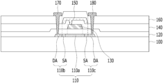
- the oxide semiconductor thin film transistor can include a substrate 100 , a semiconductor layer 110 , a first gate insulating layer 120 , a gate electrode 130 , a second gate insulating layer 140 , an auxiliary electrode 150 , an interlayer insulating layer 160 , a source electrode 170 and a drain electrode 180 .
- the substrate 100 can support various components of a display device.
- the substrate 100 can be composed of glass or a plastic material having flexibility.
- the substrate 100 can be formed of, for example, polyimide (PI).
- PI polyimide
- the formation process of the display device can be performed in the state in which a support substrate composed of glass is located under the substrate 100 , and the support substrate can be released after the formation process of the display device is completed. Further, a back plate for supporting the substrate 100 can be located under the substrate 100 after the support substrate is released.
- the substrate 100 is formed of polyimide (PI)
- moisture can permeate the semiconductor layer 110 or a light-emitting device by passing through the substrate 100 formed of polyimide (PI), and the performance of the display device can be deteriorated.
- the substrate 100 can include double-layered polyimide (PI) in order to prevent the performance of the display device from being deteriorated due to the permeation of the moisture.
- An inorganic film can be formed between the two polyimides (PI) of the substrate 100 .
- the moisture passing through the outer polyimide (PI) of the substrate 100 can be blocked by the inorganic film, and the reliability for the performance of the oxide semiconductor thin film transistor can be improved.
- the inorganic film can have a single layer structure composed of silicon nitride (SiNx) or silicon oxide (SiOx), or a multi-layer structure thereof.
- the semiconductor layer 110 can be disposed on the substrate 100 .
- the semiconductor layer 110 can include a channel region 110 a , a source region 110 b and a drain region 110 c .
- a channel can be formed in the channel region 110 a of the semiconductor layer 110 during driving the oxide semiconductor thin film transistor.
- the source region 110 b and the drain region 110 c can be disposed at both sides of the channel region 110 a .
- Each of the source region 110 b and the drain region 110 c can include a conductorization region DA and a diffusing conductorization region SA.
- the semiconductor layer 110 can be composed of an oxide semiconductor. Since the oxide semiconductor is a material having a larger band gap than silicon, electrons cannot exceed the band gap in the off state. Thus, in the oxide semiconductor thin film transistor according to the embodiment of the present disclosure, off-current of the semiconductor layer 110 can be low. Therefore, the oxide semiconductor thin film transistor according to the embodiment of the present disclosure can be suitable for a switching thin film transistor that has a short on-time and a long off-time.
- the present disclosure is not limited thereto.
- the oxide semiconductor thin film transistor according to the embodiment of the present disclosure can be used as a driving thin film transistor according to the characteristics of the display device.
- the oxide semiconductor thin film transistor according to the embodiment of the present disclosure can be suitable for a high-resolution display device, because the capacitance of auxiliary capacitor can be reduced due to the small off-current.
- the semiconductor layer 110 can be composed of IGZO (indium-gallium-zinc-oxide). However, the present disclosure is not limited thereto.
- the semiconductor layer 110 can be composed of various metal oxides, such as IZO (indium zinc oxide), IGTO (indium-gallium-tin-oxide), and IGO (indium-gallium-oxide), rather than IGZO.
- a conductive characteristic of the metal oxide can be improved by a doping process in which impurities are injected.
- the channel region 110 a , the source region 110 b and the drain region 110 c of the semiconductor layer 110 can be formed by the doping process to be described later.
- the channel region 110 a of the semiconductor layer 110 may not contain impurities.
- the source region 110 b and the drain region 110 c of the layer semiconductor 110 can be conductorized by injection of the impurities.
- the source region 110 b and the drain region 110 c of the semiconductor layer 110 can include the impurities.
- the source region 110 b can mean a region of the semiconductor layer 110 connected to the source electrode 170 .
- the drain region 110 c can mean a region of the semiconductor layer 110 connected to the drain electrode 180 .
- the source region 110 b and the drain region 110 c can be formed by the doping process in which one of group 3 elements, such as boron is injected into the semiconductor layer 110 formed of a metal oxide.
- the channel region 110 a can mean a region of the semiconductor layer 110 that is not conductorized, and remains in state of an oxide semiconductor.
- the channel region 110 a can be formed by self-align method using the auxiliary electrode 150 .
- the auxiliary electrode 150 can serve as a mask blocking the impurities during the doping process, so that the channel region 110 a can be defined without considering an additional mask process and alignment margin.
- the conductorization region DA of the source region 110 b and the drain region 110 c can be a region exposed by the auxiliary electrode 150 .
- the conductorization region DA of the source region 110 b and the drain region 110 c can be a region in which the impurities are directly added during the doping process. The impurities are not direct added into a central portion of the semiconductor layer 110 which is not exposed by the auxiliary electrode 150 during the doping process.
- a part of the both sides of the central portion can be conductorized by some of doping material diffused into the channel region in a doping process of the entire substrate, or by impurities such as hydrogen diffused into the channel region in a process of forming the passivation layer including silicon nitride (SiNx) containing a large amount of hydrogen.
- the diffusing conductorization region SA of the source region 110 b and the drain region 110 c can be disposed a part of the both sides of the central portion of the semiconductor layer 110 which is not exposed by the auxiliary electrode 150 .
- the diffusing conductorization region SA is conductorized by a material diffused in the doping process or the process of forming the passivation layer, the diffusing conductorization region SA can include group 3 elements, such as hydrogen or boron.
- the diffusing conductorization region SA can be formed so as overlap both ends of the auxiliary electrode 150 .
- the diffusing conductorization region SA can be formed so as not to overlap by being spaced apart from both ends of the gate electrode 150 .
- an end of diffusing the conductorization region SA near to the gate electrode can be formed so as being spaced away from an end of the gate electrode 130
- another end of the diffusing conductorization region SA far from the gate electrode can be formed so as being corresponding to an end of the auxiliary electrode 150 .
- the diffusing conductorization region SA of the semiconductor layer 110 can be formed so as not to overlap the gate electrode 150 . Therefore, in the oxide semiconductor thin film transistor according to the embodiment of the present disclosure, the generation of the parasitic capacitance Cgs between the gate electrode 130 and the semiconductor layer 110 can be prevented, and high-speed driving can be realized.
- the first gate insulating layer 120 can be disposed on the semiconductor layer 110 .
- the first gate insulating layer 120 can have a single layer structure composed of silicon nitride (SiNx) or silicon oxide (Siox), or a multi-layer structure thereof.
- a contact hole for connecting the source electrode 170 to the source region 110 b of the semiconductor layer 110 , and a contact hole for connecting the drain electrode 180 to the drain region 110 c of the semiconductor layer 110 can be formed in the first gate insulating layer 120 .
- the gate electrode 130 can be disposed on the first gate insulating layer 120 .
- the gate electrode 130 can have a single layer structure composed of at least one of molybdenum (Mo), copper (Cu), titanium (Ti), aluminum (Al), chromium (Cr), gold (Au), nickel (Ni) and neodymium (Nd) or an alloy thereof, or a multi-layer structure thereof.
- Mo molybdenum
- Cu copper
- Ti titanium
- Al aluminum
- Cr chromium
- Au gold
- Ni nickel
- Nd neodymium
- the gate electrode 130 can be formed so as to overlap the channel region 110 a of the semiconductor layer 110 .
- the gate electrode 130 can be formed so as not to overlap the diffusing conductorization region SA of the source region 110 b and the drain region 110 c.
- the second gate insulating layer 140 can be disposed on the first gate insulating layer 120 and the gate electrode 130 .
- the second gate insulating layer 140 can have a single layer structure composed of silicon nitride (SiNx) or silicon oxide (SiOx), or a multi-layer structure thereof.
- a contact hole for connecting the source electrode 170 to the source region 110 b of the semiconductor layer 110 , a contact hole for connecting the drain electrode 180 to the drain region 110 c of the semiconductor layer 110 , and a gate contact hole for connecting the auxiliary electrode 150 to the gate electrode 130 can be formed in the second gate insulating layer 140 .
- the auxiliary electrode 150 can be disposed on the second gate insulating layer 140 .
- the auxiliary electrode 150 can be formed of a metal capable of collecting hydrogen, such as titanium (Ti).
- the auxiliary electrode 150 can collect hydrogen generated inside the display device. Therefore, the diffusion of the impurities, such as hydrogen which is generated inside the display device during forming the passivation layer including silicon nitride (SiNx) containing a large amount of hydrogen into the semiconductor layer 110 can be prevented. Thereby, in the oxide semiconductor thin film transistor according to the embodiment of the present disclosure, the characteristics of the performance can be improved.
- the auxiliary electrode 150 can be formed on the second gate insulating layer 140 so as overlap the gate electrode 130 , the channel region 110 a of the semiconductor layer 110 , and the diffusing conductorization region SA of the source region 110 b and the drain region 110 c.
- a size of the auxiliary electrode 150 can be smaller than that of the semiconductor layer 110 .
- the size of the auxiliary electrode 150 can be larger than that of the gate electrode 130 .
- an end of the auxiliary electrode 150 can be formed between an end of the semiconductor layer 110 and an end of the gate electrode 130 , in plan-view.
- the auxiliary electrode 150 can be formed so as cover the gate electrode 130 .
- the auxiliary electrode 150 can be formed so as include both ends of the gate electrode 130 .
- the auxiliary electrode 150 can be connected to the gate electrode 130 through the gate contact hole which is formed in the second gate insulating layer 140 .
- the generation of the parasitic capacitance Cgs can be prevented by removing an overlapping region between the diffusing conductorization region SA of the oxide semiconductor layer 110 and the gate electrode 130 .
- the oxide semiconductor thin film transistor according to the embodiment of the present disclosure can prevent a length of the effective channel in the semiconductor layer 110 from being decreased. Therefore, in the oxide semiconductor thin film transistor according to the embodiment of the present disclosure, the mobility of the electrons in the semiconductor layer 110 can be improved, and high-speed driving can be realized.
- the interlayer insulating layer 160 can be disposed on the second gate insulating layer 140 and the auxiliary electrode 150 .
- the interlayer insulating layer 160 can have a single layer structure composed of silicon nitride (SiNx) or silicon oxide (SiOx), or a multi-layer structure thereof.
- a contact hole for connecting the source electrode 170 to the source region 110 b of the semiconductor layer 110 , and a contact hole for connecting the drain electrode 180 to the drain region 110 c of the semiconductor layer 110 can be formed in the interlayer insulating layer 160 .
- the source electrode 170 and the drain electrode 180 of the oxide semiconductor thin film transistor can be disposed on the interlayer insulating layer 160 .
- the source electrode 170 and the drain electrode 180 of the oxide semiconductor thin film transistor can be respectively connected to the semiconductor layer 110 through the contact holes which are formed in the first gate insulating layer 120 , the second gate insulating layer 140 and the interlayer insulating layer 160 .
- the source electrode 170 can be connected to the source region 110 b of the semiconductor layer 110 through the contact holes which are formed in the first gate insulating layer 120 , the second gate insulating layer 140 and the interlayer insulating layer 160
- the drain electrode 180 can be connected to the drain region 110 c of the semiconductor layer 110 through the contact holes which are formed in the first gate insulating layer 120 , the second gate insulating layer 140 and the interlayer insulating layer 160 .
- the source electrode 170 and the drain electrode 180 can be formed of the same material.
- Each of the source electrode 170 and the drain electrode 180 can have a single layer structure composed of at least one of molybdenum (Mo), copper (Cu), titanium (Ti), aluminum (Al), chromium (Cr), gold (Au), nickel (Ni) and neodymium (Nd) or an alloy thereof, or a multi-layer structure thereof.
- each of the source electrode 170 and the drain electrode 180 can have a triple-layer structure of conductive materials, such as titanium (Ti)/aluminum (Al)/titanium (Ti).
- the present disclosure is not limited thereto.
- FIGS. 3 A to 3 K are cross-sectional views sequentially showing a method of forming the oxide semiconductor thin film transistor according to the embodiment of the present disclosure.
- the method of forming the oxide semiconductor thin film transistor according to the embodiment of the present specification will be described with reference to FIGS. 3 A to 3 K .
- the method of forming the oxide semiconductor thin film transistor according to the embodiment of the present specification can include a step of forming a semiconductor layer 110 a composed of an oxide semiconductor on a substrate 100 .
- step can be composed of one or more sub-steps, or one or more of processes.
- the step of forming the semiconductor layer 110 a can include a process of depositing the oxide semiconductor on an entire surface of the substrate 100 .
- the oxide semiconductor can include at least one of various metal oxides, such as IGZO (indium-gallium-zinc-oxide), IGO (indium-gallium-oxide), IGTO (indium-gallium-tin-oxide), and
- the step of forming the semiconductor layer 110 a can include a process of patterning the oxide semiconductor using a first mask.
- the method of forming the oxide semiconductor thin film transistor according to the embodiment of the present specification can include a process of forming a light-blocking layer to protect the semiconductor layer 110 from external light on the substrate 100 , before forming the semiconductor layer 110 a . Further, the method of forming the oxide semiconductor thin film transistor according to the embodiment of the present specification can include a process of forming a buffer layer covering the entire surface of the substrate 100 on the light-blocking layer, before forming the semiconductor layer 110 a.
- the method of forming the oxide semiconductor thin film transistor can include a step of forming a first gate insulating layer 120 by depositing an insulating material, such as silicon nitride (SiNx) or silicon oxide (SiOx) on the entire surface of the substrate 100 in which the semiconductor layer 110 a is formed.
- the first gate insulating layer 120 can have a single layer structure composed of silicon nitride (SiNx) or silicon oxide (SiOx), or a multi-layer structure thereof.
- the method of forming the oxide semiconductor thin film transistor according to the embodiment of the present specification can include a step of depositing a metal material on the first gate insulating layer 120 , and a step of forming a gate electrode 130 by pattering the metal material using a second mask.
- the gate electrode 130 can be disposed so as overlap the semiconductor layer 110 a.
- the gate electrode 130 can have a single layer structure composed of at least one of molybdenum (Mo), copper (Cu), titanium (Ti), aluminum (Al), chromium (Cr), gold (Au), nickel (Ni) and neodymium (Nd) or an alloy thereof, or a multi-layer structure thereof.
- Mo molybdenum
- Cu copper
- Ti titanium
- Al aluminum
- Cr chromium
- Au gold
- Ni nickel
- Nd neodymium
- the method of forming the oxide semiconductor thin film transistor can include a step of forming a second gate insulating layer 140 by depositing an insulating material, such as silicon nitride (SiNx) or silicon oxide (SiOx) on the entire surface of the substrate 100 in which the first gate insulating layer 120 and the gate electrode 130 are formed.
- the second gate insulating layer 140 can have a single layer structure composed of silicon nitride (SiNx) or silicon oxide (Siox), or a multi-layer structure thereof.
- the method of forming the oxide semiconductor thin film transistor according to the embodiment of the present specification can include a step of forming a gate contact hole GH exposing the gate electrode 130 by pattering the second gate insulating layer 140 using a third mask.
- the method of forming the oxide semiconductor thin film transistor can include a step of depositing a metal material on the second gate insulating layer 140 in which the gate contact hole GH is formed, and a step of forming an auxiliary electrode 150 by patterning the metal material using a fourth mask.
- the auxiliary electrode 150 can be disposed so as overlap the gate electrode 130 and the channel region 110 a of the semiconductor layer 110 .
- the auxiliary electrode 150 can be disposed so as overlap a diffusing conductorization region SA of the source region 110 b and the drain region 110 c , which are formed by a sub-sequent process.
- the auxiliary electrode 150 can be formed of a metal capable of collecting hydrogen, such as titanium (Ti).
- the auxiliary electrode 150 can be formed so as cover the gate electrode 130 .
- the auxiliary electrode 150 can be formed so as include both ends of the gate electrode 130 .
- the auxiliary electrode 150 can be connected to the gate electrode 130 through the gate contact hole GH which is formed in the second gate insulating layer 140 .
- the method of forming the oxide semiconductor thin film transistor according to the embodiment of the present specification can include a step of performing a doping process on the entire surface of the substrate 100 .
- the doping process includes a process of injecting impurities composed of at least one of group 3 elements, such as boron into the semiconductor layer 110 a.
- the conditions of the doping process can include the acceleration voltage of 40 to 100 keV and the current density of 1E15/cm3.
- the doping process can include a process of injecting impurities with the acceleration voltage of 40 to 100 kev and the current density of 1E15/cm3 into the substrate 100 in which the second gate insulating layer 140 is formed.
- the semiconductor layer 110 can be formed by the doping process as shown in FIG. 3 G .
- the semiconductor layer 110 can include a channel region 110 a , the source region 110 b and the drain region 110 c .
- the source region 110 b and the drain region 110 c can include a region exposed by the auxiliary electrode 150 .
- the source region 110 b and the drain region 110 c can include a region being conductorized by adding the impurities.
- the channel region 110 a can be not conductorized.
- the channel region 110 a can be a region in which the impurities are not added by blocking due to the auxiliary electrode 150 .
- the source region 110 b and the drain region 110 c of the semiconductor layer 110 which are conductorized can have low-resistance.
- the device performance of the oxide semiconductor thin film transistor according to the embodiment of the present disclosure can be improved.
- the source region 110 b and the drain region 110 c can be formed by the doping process of injecting at least one of group 3 elements, such as boron into the semiconductor layer 110 formed of a metal oxide.
- Each of the source region 110 b and the drain region 110 c can include a conductorization region DA.
- the conductorization region DA of the source region 110 b and the drain region 110 c can be a region which is exposed by the auxiliary electrode 150 , so that the impurities are directly added during the doping process.
- the part of the both sides of the central portion can be conductorized by diffusion of some impurities into the channel region 110 a in a process of doping the entire substrate, or by diffusion of impurities such as hydrogen into the channel region 110 a in a process of forming a passivation layer including silicon nitride (SiNx) containing a large amount of hydrogen.
- the part of the both sides of the central portion conductorized by diffusion can be defined as a diffusing conductorization region SA.
- each of the source region 110 b and the drain region 110 c can include the diffusing conductorization region SA disposed closer the region channel 110 a than the conductorization region DA.
- the diffusing conductorization region SA is conductorized by a material diffused in the doping process or the process of forming the passivation layer, the diffusing conductorization region SA can include group 3 elements, such as hydrogen or boron.
- the diffusing conductorization region SA can be formed so as overlap both ends of the auxiliary electrode 150 .
- the diffusing conductorization region SA can be formed so as not to overlap by being spaced apart from both ends of the gate electrode 130 .
- an end of the diffusing conductorization region SA near top the gate electrode can be formed so as being spaced away from an end of the gate electrode 130
- another end of the diffusing conductorization region SA far from the gate electrode can be formed so as being corresponding to an end of the auxiliary electrode 150 .
- the diffusing conductorization region SA of the semiconductor layer 110 can be formed so as not to overlap the gate electrode 150 . Therefore, in the method of the oxide semiconductor thin film transistor according to the embodiment of the present disclosure, the generation of the parasitic capacitance Cgs between the gate electrode 130 and the semiconductor layer 110 can be prevented, and high-speed driving can be realized.
- the generation of the parasitic capacitance Cgs can be prevented by removing an overlap region between the diffusing conductorization region SA of the semiconductor layer 110 and the gate electrode 130 .
- reducing the length of the effective channel in the semiconductor layer 110 can be prevented, the mobility of the electrons in the semiconductor layer 110 can be improved, and high-speed driving can be realized.
- the method of forming the oxide semiconductor thin film transistor can include a step of forming an interlayer insulating layer 160 on the entire surface of the substrate 100 in which the second gate insulating layer 140 and the auxiliary electrode 150 by depositing an insulating material, such as silicon nitride (SiNx) or silicon oxide (SiOx).
- the interlayer insulating layer 160 can have a single layer structure composed of silicon nitride (SiNx) or silicon oxide (SiOx), or a multi-layer structure thereof.
- the method of forming the oxide semiconductor thin film transistor according to the embodiment of the present specification can include a step of forming a source contact hole SH exposing the source region 110 b of the semiconductor layer 110 and a drain contact hole DH exposing the drain region 110 c of the semiconductor layer 110 by pattering the first gate insulating layer 120 , the second gate insulating layer 140 and the interlayer insulating layer 160 using a fifth mask.
- the method of forming the oxide semiconductor thin film transistor according to the embodiment of the present specification can include a step of depositing a source-drain metal on the interlayer insulating layer 160 in which the source contact hole SH and the drain contact hole DH are formed, and a step of forming the source electrode 170 and the drain electrode 180 by pattering the source-drain metal using a sixth mask.
- the source electrode 170 and the drain electrode 180 can have a single layer structure composed of at least one of molybdenum (Mo), copper (Cu), titanium (Ti), aluminum (Al), chromium (Cr), gold (Au), nickel (Ni) and neodymium (Nd) or an alloy thereof, or a multi-layer structure thereof.
- the source electrode 170 and the drain electrode 180 can have a triple-layer structure of conductive materials, as such titanium (Ti)/aluminum (Al)/titanium (Ti).
- the present disclosure is not limited thereto and other variations are possible.
- the source electrode 170 can be connected to the conductorization region DA of the source region 110 b which is a side of the semiconductor layer 110 through the source contact hole SH.
- the drain electrode 180 can be connected to the conductorization layer DA of the drain region 110 c which is another side of the semiconductor layer 110 through the drain contact hole DH.
- the display device can include a liquid crystal display device (LCD), a field emission display device (FED), an organic light emitting display device (OLED) and a quantum dot display device.
- LCD liquid crystal display device
- FED field emission display device
- OLED organic light emitting display device
- quantum dot display device a quantum dot display device
- the display device can include a set electronic device apparatus, a set device or a set apparatus.
- the set electronic device, the set device and the set apparatus can include a complete product or a final product including LCM or OLED module, such as a laptop computer, a TV and a computer monitor.
- the set electronic device, the set device and the set apparatus can include an automotive display apparatus or an equipment display apparatus including another type of vehicle.
- the set electronic device, the set device and the set apparatus can include a mobile electronic device apparatus of smart phone or electric pad, any wearable electronic device, an user-interface device, etc.
- the oxide semiconductor thin film transistor according to the embodiment of the present disclosure can be described as below.
- the oxide semiconductor thin film transistor according to the embodiment of the present disclosure can comprise a semiconductor layer including a channel region, a source region and a drain region, a first gate insulating layer on the semiconductor layer, a gate electrode on the first gate insulating layer, a second gate insulating layer on the gate electrode, an auxiliary electrode on the second gate insulating layer, an interlayer insulating layer on the auxiliary electrode, and a source electrode and a drain electrode on the interlayer insulating layer, wherein the source region and the drain region being disposed at both sides of the channel region, wherein the gate electrode overlapping with the channel region, and wherein the auxiliary electrode overlapping with the gate electrode.
- each of the source region and the drain region can include a conductorization region and a diffusing conductorization region.
- the diffusing conductorization region can overlap a portion of the auxiliary electrode.
- the diffusing conductorization region may not overlap with the gate electrode.
- the auxiliary electrode can include titanium.
- a side of the diffusing conductorization region can be spaced away from an end of the gate electrode, and another side of the diffusing conductorization region can be corresponding to an end of the auxiliary electrode.
- the auxiliary electrode can overlap the gate electrode, the channel region and the diffusing conductorization region.
- a width of the channel region can be formed larger than a width of the gate electrode.
- the conductorization region can include at least one of group 3 elements.
- the diffusing conductorization region can include hydrogen and/or at least one of group 3 elements.
- the group 3 elements here can include fluorine.
- the group 3 elements can include fluorine.
- a method of forming an oxide semiconductor thin film transistor can include forming an oxide semiconductor layer, depositing a first gate insulating layer on the oxide semiconductor layer, forming a gate electrode on the first gate insulating layer, depositing a second gate insulating layer on the gate electrode, forming a gate contact hole exposing the gate electrode, a step of forming an auxiliary electrode on the second gate insulating layer, doping impurities, depositing an interlayer insulating layer on the auxiliary electrode, forming contact hole and a drain contact hole, and forming a source electrode and a drain electrode, wherein the source contact hole and the drain contact hole expose the oxide semiconductor layer, and wherein the source electrode and the drain electrode are electrically connected to the oxide semiconductor layer.
- each of the source region and the drain region can include a conductorization region and a diffusing conductorization region.
- the diffusing conductorization region can overlap a portion of the auxiliary electrode.
- the diffusing conductorization region may not overlap with the gate electrode.
- the auxiliary electrode can be electrically connected to the gate electrode through a gate contact hole.
- the auxiliary electrode can include titanium.
- a width of the channel region can be formed larger than a width of gate electrode.
- a step of doping can be performed by acceleration voltage of 40 to 100 keV.
- the oxide semiconductor thin film transistor according to the embodiments of the present disclosure can include an auxiliary electrode on a gate electrode.
- the reliability can be improved.
- the oxide semiconductor thin film transistor according to the embodiments of the present disclosure can prevent the impurities generated inside the display device during the formation process from diffusing into the channel region of the semiconductor layer formed of an oxide semiconductor.
- the auxiliary electrode can be formed of a metal capable of collecting hydrogen, so that the introduction of hydrogen into the oxide semiconductor layer can be minimized.
- the device characteristics can be improved.
- the generation of the parasitic capacitance can be prevented by removing an overlapping region between the diffusing conductorization region of the oxide semiconductor layer and the gate electrode.
- the oxide semiconductor thin film transistor according to the embodiments of the present disclosure can prevent reducing a length of the effective channel in the oxide semiconductor layer.
- the mobility of the electrons in the oxide semiconductor layer can be improved, and high-speed driving can be realized.
Landscapes
- Thin Film Transistor (AREA)
Abstract
Description
Claims (9)
Applications Claiming Priority (2)
| Application Number | Priority Date | Filing Date | Title |
|---|---|---|---|
| KR10-2020-0040142 | 2020-04-02 | ||
| KR1020200040142A KR102780730B1 (en) | 2020-04-02 | 2020-04-02 | Oxide Semiconductor Thin Film Transistor And Manufacturing Thereof |
Publications (2)
| Publication Number | Publication Date |
|---|---|
| US20210313470A1 US20210313470A1 (en) | 2021-10-07 |
| US12094978B2 true US12094978B2 (en) | 2024-09-17 |
Family
ID=77921862
Family Applications (1)
| Application Number | Title | Priority Date | Filing Date |
|---|---|---|---|
| US17/220,676 Active 2041-12-29 US12094978B2 (en) | 2020-04-02 | 2021-04-01 | Oxide semiconductor thin film transistor and method of forming the same |
Country Status (2)
| Country | Link |
|---|---|
| US (1) | US12094978B2 (en) |
| KR (1) | KR102780730B1 (en) |
Families Citing this family (4)
| Publication number | Priority date | Publication date | Assignee | Title |
|---|---|---|---|---|
| CN114122008B (en) * | 2021-11-04 | 2023-05-02 | 深圳市华星光电半导体显示技术有限公司 | Array substrate, manufacturing method and mobile terminal |
| KR102864045B1 (en) | 2021-11-19 | 2025-09-23 | 엘지디스플레이 주식회사 | Thin film transistor, thin film transistor substrate and display apparatus |
| CN114937701B (en) | 2022-04-14 | 2025-05-27 | 深圳市华星光电半导体显示技术有限公司 | Array substrate and manufacturing method thereof, and display panel |
| KR20250090874A (en) * | 2023-12-13 | 2025-06-20 | 엘지디스플레이 주식회사 | Thin film transistor, manufactruing method thereof, and display apparatus comprising the same |
Citations (14)
| Publication number | Priority date | Publication date | Assignee | Title |
|---|---|---|---|---|
| US5693549A (en) * | 1994-09-13 | 1997-12-02 | Lg Semicon Co., Ltd. | Method of fabricating thin film transistor with supplementary gates |
| US6133609A (en) * | 1998-02-18 | 2000-10-17 | Nec Corporation | High-voltage thin-film transistor with sub-gate elements |
| US20050062044A1 (en) * | 2003-09-19 | 2005-03-24 | Semiconductor Energy Laboratory Co., Ltd. | Semiconductor device, method of manufacturing the same, and electronic device having the same |
| US20060255377A1 (en) * | 2005-05-12 | 2006-11-16 | Der-Wei Tu | Field effect transistor with novel field-plate structure |
| US20070145458A1 (en) * | 2005-12-26 | 2007-06-28 | Semiconductor Energy Laboratory Co., Ltd. | Semiconductor device and manufacturing method thereof |
| KR20150051824A (en) | 2013-11-05 | 2015-05-13 | 삼성디스플레이 주식회사 | Thin film transistor array substrate, organic light-emitting display apparatus and manufacturing of the thin film transistor array substrate |
| US20150206905A1 (en) * | 2013-03-05 | 2015-07-23 | Boe Technology Group Co., Ltd. | Polysilicon thin film transistor and manufacturing method thereof, array substrate |
| US20170256569A1 (en) * | 2016-03-07 | 2017-09-07 | Japan Display Inc. | Semiconductor device and display device and manufacturing method thereof |
| US20180047822A1 (en) * | 2016-08-15 | 2018-02-15 | Delta Electronics, Inc. | Semiconductor device |
| US20190115407A1 (en) * | 2017-10-13 | 2019-04-18 | Samsung Display Co., Ltd. | Display panel and method of fabricating the same |
| US20190221429A1 (en) * | 2017-01-04 | 2019-07-18 | Boe Technology Group Co., Ltd. | Methods of manufacturing thin film transistor, array substrate and display device |
| WO2019175708A1 (en) | 2018-03-16 | 2019-09-19 | 株式会社半導体エネルギー研究所 | Semiconductor device and method for manufacturing semiconductor device |
| US20190331972A1 (en) * | 2018-04-25 | 2019-10-31 | Seiko Epson Corporation | Electro-optical device and electronic apparatus |
| US20240128347A1 (en) * | 2020-01-07 | 2024-04-18 | Samsung Electronics Co., Ltd. | Semiconductor device |
-
2020
- 2020-04-02 KR KR1020200040142A patent/KR102780730B1/en active Active
-
2021
- 2021-04-01 US US17/220,676 patent/US12094978B2/en active Active
Patent Citations (15)
| Publication number | Priority date | Publication date | Assignee | Title |
|---|---|---|---|---|
| US5693549A (en) * | 1994-09-13 | 1997-12-02 | Lg Semicon Co., Ltd. | Method of fabricating thin film transistor with supplementary gates |
| US6133609A (en) * | 1998-02-18 | 2000-10-17 | Nec Corporation | High-voltage thin-film transistor with sub-gate elements |
| US20050062044A1 (en) * | 2003-09-19 | 2005-03-24 | Semiconductor Energy Laboratory Co., Ltd. | Semiconductor device, method of manufacturing the same, and electronic device having the same |
| US20060255377A1 (en) * | 2005-05-12 | 2006-11-16 | Der-Wei Tu | Field effect transistor with novel field-plate structure |
| US20070145458A1 (en) * | 2005-12-26 | 2007-06-28 | Semiconductor Energy Laboratory Co., Ltd. | Semiconductor device and manufacturing method thereof |
| US20150206905A1 (en) * | 2013-03-05 | 2015-07-23 | Boe Technology Group Co., Ltd. | Polysilicon thin film transistor and manufacturing method thereof, array substrate |
| KR20150051824A (en) | 2013-11-05 | 2015-05-13 | 삼성디스플레이 주식회사 | Thin film transistor array substrate, organic light-emitting display apparatus and manufacturing of the thin film transistor array substrate |
| US20170256569A1 (en) * | 2016-03-07 | 2017-09-07 | Japan Display Inc. | Semiconductor device and display device and manufacturing method thereof |
| US20180047822A1 (en) * | 2016-08-15 | 2018-02-15 | Delta Electronics, Inc. | Semiconductor device |
| US20190221429A1 (en) * | 2017-01-04 | 2019-07-18 | Boe Technology Group Co., Ltd. | Methods of manufacturing thin film transistor, array substrate and display device |
| US20190115407A1 (en) * | 2017-10-13 | 2019-04-18 | Samsung Display Co., Ltd. | Display panel and method of fabricating the same |
| WO2019175708A1 (en) | 2018-03-16 | 2019-09-19 | 株式会社半導体エネルギー研究所 | Semiconductor device and method for manufacturing semiconductor device |
| US20210005752A1 (en) * | 2018-03-16 | 2021-01-07 | Semiconductor Energy Laboratory Co., Ltd. | Semiconductor device and method for manufacturing semiconductor device |
| US20190331972A1 (en) * | 2018-04-25 | 2019-10-31 | Seiko Epson Corporation | Electro-optical device and electronic apparatus |
| US20240128347A1 (en) * | 2020-01-07 | 2024-04-18 | Samsung Electronics Co., Ltd. | Semiconductor device |
Non-Patent Citations (2)
| Title |
|---|
| Seo, JS et al. Solution-Processed Flexible Fluorine-doped Indium Zinc Oxide Thin-Film Transistors Fabricated on Plastic Film at Low Temperature. Sci Rep 3, 2085 (2013) (Year: 2013). * |
| Seo, JS et al. Solution-Processed Flexible Fluorine-doped Indium Zinc Oxide Thin-Film Transistors Fabricated on Plastic Film at Low Temperature. Sci Rep 3, 2085 (2013); hereinafter Seo (Year: 2013). * |
Also Published As
| Publication number | Publication date |
|---|---|
| KR102780730B1 (en) | 2025-03-12 |
| KR20210123003A (en) | 2021-10-13 |
| US20210313470A1 (en) | 2021-10-07 |
Similar Documents
| Publication | Publication Date | Title |
|---|---|---|
| US12094978B2 (en) | Oxide semiconductor thin film transistor and method of forming the same | |
| US10192992B2 (en) | Display device | |
| US20230215954A1 (en) | Thin film transistor, thin film transistor array panel including the same, and method of manufacturing the same | |
| US7176068B2 (en) | Semiconductor device and manufacturing method thereof | |
| US10367073B2 (en) | Thin film transistor (TFT) with structured gate insulator | |
| US8981359B2 (en) | Organic light emitting diode display device and method of fabricating the same | |
| US8440483B2 (en) | Method of fabricating array substrate | |
| US10186529B2 (en) | Thin film transistor substrate and display using the same | |
| US20150129865A1 (en) | Semiconductor device and method for manufacturing same | |
| US9991287B2 (en) | Thin film transistor array panel | |
| US12527087B2 (en) | Display device and manufacturing method thereof | |
| KR20160120389A (en) | Manufacturing method of thin-film transistor array substrate and thin-film transistor array substrate thereof | |
| US12022704B2 (en) | Display apparatus having an oxide semiconductor pattern | |
| US10192890B2 (en) | Transistor array panel and method of manufacturing thereof | |
| JP4540776B2 (en) | Semiconductor device and electronic equipment | |
| EP3676876B1 (en) | Thin film transistor, array substrate, display apparatus, and method of fabricating thin film transistor | |
| CN115411054B (en) | Array substrate, its fabrication method and display device | |
| KR102801061B1 (en) | Display device | |
| CN121888658A (en) | Semiconductor device and display device | |
| CN121888659A (en) | Semiconductor device and display device | |
| CN121888657A (en) | Semiconductor device and display device | |
| JP2026070463A (en) | Semiconductor and display devices | |
| JP2025059540A (en) | Semiconductor device and display device |
Legal Events
| Date | Code | Title | Description |
|---|---|---|---|
| FEPP | Fee payment procedure |
Free format text: ENTITY STATUS SET TO UNDISCOUNTED (ORIGINAL EVENT CODE: BIG.); ENTITY STATUS OF PATENT OWNER: LARGE ENTITY |
|
| AS | Assignment |
Owner name: LG DISPLAY CO., LTD., KOREA, REPUBLIC OF Free format text: ASSIGNMENT OF ASSIGNORS INTEREST;ASSIGNORS:JI, HYUK;JEON, JIN CHAE;KIM, JAE HYUN;AND OTHERS;REEL/FRAME:055816/0750 Effective date: 20210330 |
|
| STPP | Information on status: patent application and granting procedure in general |
Free format text: DOCKETED NEW CASE - READY FOR EXAMINATION |
|
| STPP | Information on status: patent application and granting procedure in general |
Free format text: NON FINAL ACTION MAILED |
|
| STPP | Information on status: patent application and granting procedure in general |
Free format text: FINAL REJECTION MAILED |
|
| STPP | Information on status: patent application and granting procedure in general |
Free format text: RESPONSE AFTER FINAL ACTION FORWARDED TO EXAMINER |
|
| STPP | Information on status: patent application and granting procedure in general |
Free format text: ADVISORY ACTION MAILED |
|
| STPP | Information on status: patent application and granting procedure in general |
Free format text: DOCKETED NEW CASE - READY FOR EXAMINATION |
|
| STPP | Information on status: patent application and granting procedure in general |
Free format text: NON FINAL ACTION MAILED |
|
| STPP | Information on status: patent application and granting procedure in general |
Free format text: RESPONSE TO NON-FINAL OFFICE ACTION ENTERED AND FORWARDED TO EXAMINER |
|
| STPP | Information on status: patent application and granting procedure in general |
Free format text: FINAL REJECTION MAILED |
|
| STPP | Information on status: patent application and granting procedure in general |
Free format text: RESPONSE AFTER FINAL ACTION FORWARDED TO EXAMINER |
|
| STPP | Information on status: patent application and granting procedure in general |
Free format text: ADVISORY ACTION MAILED |
|
| STPP | Information on status: patent application and granting procedure in general |
Free format text: DOCKETED NEW CASE - READY FOR EXAMINATION |
|
| STPP | Information on status: patent application and granting procedure in general |
Free format text: NOTICE OF ALLOWANCE MAILED -- APPLICATION RECEIVED IN OFFICE OF PUBLICATIONS |
|
| STPP | Information on status: patent application and granting procedure in general |
Free format text: PUBLICATIONS -- ISSUE FEE PAYMENT RECEIVED |
|
| STPP | Information on status: patent application and granting procedure in general |
Free format text: PUBLICATIONS -- ISSUE FEE PAYMENT VERIFIED |
|
| STCF | Information on status: patent grant |
Free format text: PATENTED CASE |