US12093205B2 - Interface conversion device - Google Patents
Interface conversion device Download PDFInfo
- Publication number
- US12093205B2 US12093205B2 US18/084,583 US202218084583A US12093205B2 US 12093205 B2 US12093205 B2 US 12093205B2 US 202218084583 A US202218084583 A US 202218084583A US 12093205 B2 US12093205 B2 US 12093205B2
- Authority
- US
- United States
- Prior art keywords
- circuit
- terminal
- usb
- coupled
- conversion device
- Prior art date
- Legal status (The legal status is an assumption and is not a legal conclusion. Google has not performed a legal analysis and makes no representation as to the accuracy of the status listed.)
- Active, expires
Links
Images


Classifications
-
- G—PHYSICS
- G06—COMPUTING OR CALCULATING; COUNTING
- G06F—ELECTRIC DIGITAL DATA PROCESSING
- G06F13/00—Interconnection of, or transfer of information or other signals between, memories, input/output devices or central processing units
- G06F13/38—Information transfer, e.g. on bus
-
- G—PHYSICS
- G06—COMPUTING OR CALCULATING; COUNTING
- G06F—ELECTRIC DIGITAL DATA PROCESSING
- G06F13/00—Interconnection of, or transfer of information or other signals between, memories, input/output devices or central processing units
- G06F13/38—Information transfer, e.g. on bus
- G06F13/382—Information transfer, e.g. on bus using universal interface adapter
- G06F13/385—Information transfer, e.g. on bus using universal interface adapter for adaptation of a particular data processing system to different peripheral devices
-
- G—PHYSICS
- G06—COMPUTING OR CALCULATING; COUNTING
- G06F—ELECTRIC DIGITAL DATA PROCESSING
- G06F13/00—Interconnection of, or transfer of information or other signals between, memories, input/output devices or central processing units
- G06F13/38—Information transfer, e.g. on bus
- G06F13/42—Bus transfer protocol, e.g. handshake; Synchronisation
- G06F13/4282—Bus transfer protocol, e.g. handshake; Synchronisation on a serial bus, e.g. I2C bus, SPI bus
-
- G—PHYSICS
- G06—COMPUTING OR CALCULATING; COUNTING
- G06F—ELECTRIC DIGITAL DATA PROCESSING
- G06F2213/00—Indexing scheme relating to interconnection of, or transfer of information or other signals between, memories, input/output devices or central processing units
- G06F2213/0042—Universal serial bus [USB]
-
- G—PHYSICS
- G06—COMPUTING OR CALCULATING; COUNTING
- G06F—ELECTRIC DIGITAL DATA PROCESSING
- G06F2213/00—Indexing scheme relating to interconnection of, or transfer of information or other signals between, memories, input/output devices or central processing units
- G06F2213/38—Universal adapter
- G06F2213/3852—Converter between protocols
Definitions
- the invention relates to an electronic device, and more particularly, to an interface conversion device.
- An interface conversion device may convert the first transmission interface of one equipment to the second transmission interface of another equipment.
- the USB transmission interface (USB connector) of a Universal Serial Bus (USB) host may be electrically connected to the DP transmission interface (DP connector) of a Display Port (DP) device via the interface conversion device. Therefore, the interface conversion device may transmit the data over a USB Type-C connector of the USB host to the DP connector of the DP device. How to implement the interface conversion device is one of many technical issues in the art.
- the invention provides an interface conversion device for transmitting data between different transmission interfaces.
- an interface conversion device includes a first Universal Serial Bus (USB) connector, a display port (DP) connector, a first physical layer circuit, a second physical layer circuit, a digital buffer, a USB controller, and a path switching circuit.
- a first terminal of the first physical layer circuit is coupled to the first USB connector.
- a first terminal of the second physical layer circuit is coupled to the DP connector.
- An output terminal of the digital buffer is coupled to a second terminal of the first physical layer circuit.
- the USB controller is coupled to the second terminal of the first physical layer circuit.
- a common terminal of the path switching circuit is coupled to a second terminal of the second physical layer circuit.
- a first selection terminal of the path switching circuit is coupled to the output terminal of the digital buffer.
- a second selection terminal of the path switching circuit is coupled to a DP output terminal of the USB controller.
- an operation mode of the interface conversion device is a DP ALT mode
- the path switching circuit is selectively configured to connect the common terminal with the first selection terminal electrically.
- the operation mode of the interface conversion device is a tunneling mode
- the path switching circuit is selectively configured to connect the common terminal with the second selection terminal electrically.
- the interface conversion device includes a USB connector, a DP connector, a digital buffer, a USB controller, a path switching circuit, an analog-to-digital conversion circuit, and a digital-to-analog conversion circuit.
- the analog-to-digital conversion circuit is coupled to the USB connector, the digital buffer, and the USB controller.
- the analog-to-digital conversion circuit converts a first analog data signal to first digital data, and outputs the first digital data to the digital buffer and the USB controller.
- a first selection terminal of the path switching circuit is coupled to an output terminal of the digital buffer.
- a second selection terminal of the path switching circuit is coupled to a DP output terminal of the USB controller.
- the path switching circuit When an operation mode of the interface conversion device is a DP ALT mode, the path switching circuit is selectively configured to connect a common terminal of the path switching circuit with the first selection terminal electrically. When the operation mode of the interface conversion device is a tunneling mode, the path switching circuit is selectively configured to connect the common terminal with the second selection terminal electrically.
- the digital-to-analog conversion circuit is coupled to the path switching circuit and the DP connector. The digital-to-analog conversion circuit converts second digital data to a second analog data signal, and outputs the second analog data signal to the DP connector.
- the interface conversion device of the embodiments of the invention may convert an analog domain signal to a digital domain signal to the digital buffer and the USB controller. Based on different operation modes of the interface conversion device, the interface conversion device may choose to convert the digital domain signal over the digital buffer or the USB controller to the analog domain signal to the DP connector. Therefore, the interface conversion device may transmit data between different transmission interfaces.
- FIG. 1 is a circuit block diagram of an interface conversion device according to an embodiment of the invention.
- FIG. 2 is a schematic circuit block diagram of a USB controller shown according to an embodiment of the invention.
- FIG. 3 is a circuit block diagram of an interface conversion device according to another embodiment of the invention.
- FIG. 4 is a circuit block diagram of an interface conversion device according to another embodiment of the invention.
- FIG. 5 and FIG. 6 are circuit block diagrams of a physical layer circuit shown according to an embodiment of the invention.
- FIG. 7 is a schematic circuit block diagram of a USB controller shown according to an embodiment of the invention.
- FIG. 8 is a schematic circuit block diagram of a USB controller shown according to another embodiment of the invention.
- Coupled to (or connected to) used in the entire text of the specification of the present application (including claims) may refer to any direct or indirect connecting means.
- first device may be directly connected to the second device, or the first device may be indirectly connected to the second device via other devices or certain connecting means.
- Terms such as “first” and “second” mentioned in the entire specification of the present application (including the claims) are used to name the elements or to distinguish different embodiments or ranges, and are not used to restrict the upper or lower limits of the number of elements, nor are they used to limit the order of the elements.
- FIG. 1 is a circuit block diagram of an interface conversion device 100 according to an embodiment of the invention.
- the interface conversion device 100 shown in FIG. 1 includes a Universal Serial Bus (USB) connector 110 , a display port (DP) connector 120 , power delivery (PD) controller 130 , a physical layer circuit 140 , a digital buffer 150 , a USB controller 160 , a path switching circuit 170 , and a physical layer circuit 180 .
- the USB connector 110 may be a USB upstream-facing port (UFP) specified by the USB specification
- the DP connector 120 may be a downstream-facing port (DFP).
- UFP USB upstream-facing port
- DFP downstream-facing port
- the PD controller 130 is coupled between a configuration channel (CC) pin of the USB connector 110 and the path switching circuit 170 .
- the CC pin may include a CC1 pin and/or a CC2 pin specified by the USB specification.
- the PD controller 130 may exchange configuration information with a USB host (not shown) via the CC pin of the USB connector 110 , and then determine the operation mode of the interface conversion device 100 according to the configuration information. Based on practical applications, the host may include a computer, a tablet computer, a mobile phone, or other electronic devices having a USB-C connector.
- the PD controller 130 may control the path switching operation of the path switching circuit 170 according to the operation mode.
- the first terminal of the physical layer circuit 140 is coupled to the data transmission pin of the USB connector 110 .
- the physical layer circuit 140 may be coupled to four high-speed lanes of the USB-C connector specified by the USB specification: a transmitting (TX) pin pair TX1, a receiving (RX) pin pair RX1, a transmitting pin pair TX2, and a receiving pin pair RX2.
- the physical layer circuit 140 may convert the analog domain signal to a digital domain signal to the digital buffer 150 and the USB controller 160 .
- the physical layer circuit 140 may include a USB physical layer circuit or other circuits specified by the USB specification.
- the physical layer circuit 140 may include a TX circuit and an RX circuit specified by the USB specification.
- the physical layer circuit 140 may include an analog-to-digital conversion circuit and/or a digital-to-analog conversion circuit.
- the analog-to-digital conversion circuit (not shown) may convert the analog data signal to digital data, and output the digital data to the digital buffer 150 and the USB controller 160 .
- the digital-to-analog converting circuit (not shown) may convert the digital data over the digital buffer 150 or the USB controller 160 to an analog data signal, and output the analog data signal to the USB connector 110 .
- the output terminal of the digital buffer 150 is coupled to the second terminal of the physical layer circuit 140 .
- the digital buffer 150 may include a first-in and first-out (FIFO) buffer or other digital buffer circuits.
- FIFO first-in and first-out
- the digital buffer 150 may compensate for clock jitter between the USB connector 110 and the DP connector 120 .
- the USB controller 160 is coupled to the second terminal of the physical layer circuit 140 .
- the USB controller 160 may include a USB controller and/or other USB signal processing circuits specified by the USB specification.
- the USB controller 160 may include a link layer, a transport layer, and/or a protocol layer specified by the USB specification.
- the USB controller 160 may process the digital data over the second terminal of the physical layer circuit 140 to generate native DP data to the physical layer circuit 180 .
- the tunneling mode may include a DP tunneling mode or other tunneling modes.
- the first terminal of the physical layer circuit 180 is coupled to the data transmission pin of the DP connector 120 .
- the physical layer circuit 180 may be coupled to four main link lanes of the DP connector specified by the DP specification.
- the second terminal of the physical layer circuit 180 is coupled to the common terminal of the path switching circuit 170 .
- the physical layer circuit 180 may convert the digital domain signal to an analog domain signal to the DP connector 120 .
- the physical layer circuit 180 may include a USB physical layer circuit specified by the USB specification, a physical layer circuit specified by the DP specification, or other circuits.
- the physical layer circuit 180 may include a digital-to-analog conversion circuit.
- the digital-to-analog conversion circuit (not shown) may convert the digital data to an analog data signal, and output the analog data signal to the DP connector 120 .
- the first selection terminal of the path switching circuit 170 is coupled to the output terminal of the digital buffer 150 .
- the second selection terminal of the path switching circuit 170 is coupled to the DP output terminal of the USB controller 160 .
- the path switching circuit 170 is selectively configured to connect the common terminal with the first selection terminal electrically, so as to transmit the native DP data output from the digital buffer 150 to the physical layer circuit 180 .
- the path switching circuit 170 is selectively configured to connect the common terminal with the second selection terminal electrically, so as to transmit the native DP data output from the USB controller 160 to the physical layer circuit 180 .
- the specific implementation of the physical layer circuit 140 and the physical layer circuit 180 may be determined according to actual design.
- the circuit architecture of the physical layer circuit 140 is the same as the circuit architecture of the physical layer circuit 180 .
- the physical layer circuit 140 and the physical layer circuit 180 may be general (or analog) physical layer circuits, so that the interfaces of the USB connector 110 and the DP connector 120 are almost symmetrical.
- the interface conversion device 100 of an embodiment above may convert the analog domain signal to the digital domain signal (native DP data) to the digital buffer 150 and the USB controller 160 . Based on different operation modes of the interface conversion device 100 , the interface conversion device 100 may choose to convert the native DP data output from the digital buffer 150 to a DP analog domain signal to the DP connector 120 , or choose to convert the native DP data over the USB controller 160 to a DP analog domain signal to the DP connector 120 . Therefore, the interface conversion device 100 may transmit data between different transmission interfaces.
- FIG. 2 is a schematic circuit block diagram of the USB controller 160 shown according to an embodiment of the invention.
- the USB controller 160 shown in FIG. 2 may be used as one of many implementation examples of the USB controller 160 shown in FIG. 1 .
- the USB controller 160 includes a USB4 router 161 and a DP output adapter 162 .
- the USB router 161 is coupled to the second terminal of the physical layer circuit 140 .
- the USB4 router 161 may perform operations such as tunneling packets parsing, segmentation, routing, and so on. Based on actual design, the USB router 161 may include a USB controller and/or other USB signal processing circuits specified by the USB4 specification.
- the USB4 router 161 may include a link layer and/or a transport layer specified by the USB4 specification.
- the DP output adapter 162 is coupled to the USB4 router 161 .
- the DP output adapter 162 may convert tunneling packets to native DP packets. Based on actual design, the DP output adapter 162 may include a DP adapter and/or other DP adapter circuits specified by the USB4 specification.
- the output terminal of the DP output adapter 162 is used as the DP output terminal of the USB controller 160 to be coupled to the second selection terminal of the path switching circuit 170 .
- FIG. 3 is a circuit block diagram of an interface conversion device 300 according to another embodiment of the invention.
- the interface conversion device 300 shown in FIG. 3 includes a USB connector 310 , a DP connector 320 , a PD controller 330 , an analog-to-digital conversion circuit 340 , a digital buffer 350 , a USB controller 360 , a path switching circuit 370 , and a digital-to-analog conversion circuit 380 .
- USB controller 360 shown in FIG. 3 is as provided in the relevant description of the USB controller 160 shown in FIG. 2 .
- the analog-to-digital conversion circuit 340 is coupled to the USB connector 310 , the digital buffer 350 , and the USB controller 360 .
- the analog-to-digital conversion circuit 340 may convert a first analog data signal to first digital data, and output the first digital data to the digital buffer 350 and the USB controller 360 .
- the digital-to-analog conversion circuit 380 is coupled to the path switching circuit 370 and the DP connector 320 .
- the digital-to-analog conversion circuit 380 may convert second digital data to a second analog data signal, and output the second analog data signal to the DP connector 320 .
- the path switching circuit 370 may be selectively configured to connect the common terminal of the path switching circuit 370 with the first selection terminal electrically, so as to transmit the native DP data output from the digital buffer 350 to the digital-to-analog conversion circuit 380 .
- the path switching circuit 370 may be selectively configured to connect the common terminal with the second selection terminal electrically, so as to transmit the native DP data output from the USB controller 360 to the digital-to-analog conversion circuit 380 .
- FIG. 4 is a circuit block diagram of an interface conversion device 400 according to another embodiment of the invention.
- the interface conversion device 400 shown in FIG. 4 includes a USB connector 410 , a USB connector 415 , a DP connector 420 , a PD controller 430 , a physical layer circuit 440 , a digital buffer 450 , a USB controller 460 , a path switching circuit 470 , a physical layer circuit 480 , and a physical layer circuit 490 .
- the data transmission between the physical layer circuit 440 and the USB controller 460 may be bidirectional transmission.
- the USB connector 410 may be a USB upstream-facing port (UFP) specified by the USB specification
- the USB connector 415 may be a USB downstream-facing port (DFP) specified by the USB specification.
- the first terminal of the physical layer circuit 490 is coupled to the USB connector 415 .
- the second terminal of the physical layer circuit 490 is coupled to the USB downstream terminal of the USB controller 460 .
- the physical layer circuit 490 may include a USB physical layer circuit or other circuits specified by the USB specification.
- the physical layer circuit 490 may include a TX circuit and an RX circuit specified by the USB specification.
- the physical layer circuit 490 may include an analog-to-digital conversion circuit and/or a digital-to-analog conversion circuit.
- the specific implementation of the physical layer circuit 440 , the physical layer circuit 480 , and the physical layer circuit 490 may be determined according to actual design.
- the circuit architectures of the physical layer circuit 440 , the physical layer circuit 480 , and the physical layer circuit 490 are all the same.
- the physical layer circuits 440 , 480 , and 490 may be generic (or analog) physical layer circuits such that the interfaces of the USB connector 110 and the USB connector 415 are nearly symmetrical.
- the PD controller 430 may exchange configuration information with a USB host (not shown) via the CC pin of the USB connector 410 , and then determine the operation mode of the interface conversion device 400 according to the configuration information.
- the operation mode (path switching) of the physical layer circuit 440 , the physical layer circuit 480 , and the physical layer circuit 490 may be controlled by the PD controller 430 .
- the physical layer circuit 440 , the physical layer circuit 480 , and the physical layer circuit 490 may receive configuration information from the CC pin of the USB connector 410 , so as to determine the operation mode of the physical layer circuits 440 , 480 , and 490 according to the configuration information.
- FIG. 5 is a circuit block diagram of the physical layer circuit 440 shown according to an embodiment of the invention.
- the physical layer circuit 440 shown in FIG. 5 includes a switch SW51, a receiver (RX) circuit 510 , a transmitter (TX) circuit 520 , and a switch SW52.
- the common terminal of the switch SW51 is coupled to the USB connector 410 .
- the first selection terminal of the switch SW51 is coupled to the input terminal of the RX circuit 510 .
- the second selection terminal of the switch SW51 is coupled to the output terminal of the TX circuit 520 .
- the first selection terminal of the switch SW52 is coupled to the output terminal of the RX circuit 510 .
- the second selection terminal of the switch SW52 is coupled to the input terminal of the TX circuit 520 .
- the common terminal of the switch SW52 is coupled to the digital buffer 450 and the USB controller 460 .
- the operation mode (path switching) of the switch SW51 and the switch SW52 may be controlled by the PD controller 430 .
- the switch SW51 and the switch SW52 may receive configuration information from the CC pin of the USB connector 410 , and then determine the operation mode of the switches SW51 and SW52 according to the configuration information. Based on the configuration information of the CC pin, the switch SW51 may couple the USB connector 410 to the input terminal of the RX circuit 510 , and the switch SW52 may couple the output terminal of the RX circuit 510 to the digital buffer 450 and the USB controller 460 .
- FIG. 6 is a circuit block diagram of the physical layer circuit 480 (or the physical layer circuit 490 ) shown according to an embodiment of the invention.
- the physical layer circuit 480 (or 490 ) shown in FIG. 6 includes a switch SW61, a receiver (RX) circuit 610 , a transmitter (TX) circuit 620 , and a switch SW62.
- the common terminal of the switch SW61 is coupled to the path switching circuit 470 (or the USB controller 460 ).
- the first selection terminal of the switch SW61 is coupled to the output terminal of the RX circuit 610 .
- the second selection terminal of the switch SW61 is coupled to the input terminal of the TX circuit 620 .
- the first selection terminal of the switch SW62 is coupled to the input terminal of the RX circuit 610 .
- the second selection terminal of the switch SW62 is coupled to the output terminal of the TX circuit 620 .
- the common terminal of the switch SW62 is coupled to the DP connector 420 (or the USB connector 415 ).
- the operation mode (path switching) of the switch SW61 and the switch SW62 may be controlled by the PD controller 430 .
- the switch SW61 and the switch SW62 may receive configuration information from the CC pin of the USB connector 410 , and then determine the operation mode of the switches SW61 and SW62 according to the configuration information.
- the switch SW61 may couple the path switching circuit 470 (or the USB controller 460 ) to the input terminal of the TX circuit 620 , and the switch SW62 may couple the output terminal of the TX circuit 620 to the DP connector 420 (or the USB connector 415 ).
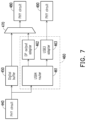
- FIG. 7 is a schematic circuit block diagram of a USB controller 460 shown according to an embodiment of the invention.
- the USB controller 460 shown in FIG. 7 may be used as one of many implementation examples of the USB controller 460 shown in FIG. 4 .
- the USB controller 460 includes a USB4 router 461 , a DP output adapter 462 , and a USB3 adapter 463 .
- the USB4 router 461 and the DP output adapter 462 shown in FIG. 7 are as provided in the relevant descriptions of the USB4 router 161 and the DP output adapter 162 shown in FIG. 2 , and are therefore not repeated herein.
- the first terminal of the USB3 adapter 463 shown in FIG. 7 is coupled to the USB4 router 461 .
- the USB3 adapter 463 may convert USB tunneling packets to native USB packets.
- the second terminal of the USB3 adapter 463 is used as the USB downstream terminal of the USB controller 460 to be coupled to the second terminal of the physical layer circuit 490 .
- the USB3 adapter 463 may include a USB3 adapter and/or other USB adapter circuits specified by the USB4 specification.
- the path switching circuit 470 may be selectively configured to connect the common terminal with the second selection terminal electrically, so as to transmit the native DP data output from the DP output adapter 462 to the physical layer circuit 480 . Additionally, in another embodiment, the USB3 adapter 463 may output native USB3 data to the physical layer circuit 490 in the tunneling mode.
- the path switching circuit 470 may be selectively configured to transmit the native DP data over the four high-speed lanes output from the digital buffer 450 to the digital-to-analog conversion circuit 480 .
- the path switching circuit 470 may be selectively configured to transmit the native DP data output from the digital buffer 450 (the DP data over the two high-speed lanes of the USB connector 410 ) to the digital-to-analog conversion circuit 480 .
- the USB3 adapter 463 may output native USB3 data (USB data over the other two high-speed lanes of the USB connector 410 ) to the physical layer circuit 490 .
- FIG. 8 is a schematic circuit block diagram of the USB controller 460 shown according to another embodiment of the invention.
- the USB controller 460 shown in FIG. 8 may be used as one of many implementation examples of the USB controller 460 shown in FIG. 4 .
- the USB controller 460 includes the USB4 router 461 , the DP output adapter 462 , and the USB3 adapter 463 .
- the USB4 router 461 , the DP output adapter 462 , and the USB3 adapter 463 shown in FIG. 8 are as provided in the relevant descriptions of the USB4 router 461 , the DP output adapter 462 , and the USB3 adapter 463 shown in FIG. 7 and are therefore not repeated herein.
- FIG. 8 is a schematic circuit block diagram of the USB controller 460 shown according to another embodiment of the invention.
- the USB controller 460 shown in FIG. 8 may be used as one of many implementation examples of the USB controller 460 shown in FIG. 4 .
- the USB controller 460 includes the USB4 router 461 , the
- the data over the 1-pair USB high-speed lane of the physical layer circuit 440 may bypass the USB4 router 461 and go directly to the USB3 adapter 463 .
Landscapes
- Engineering & Computer Science (AREA)
- Theoretical Computer Science (AREA)
- Physics & Mathematics (AREA)
- General Engineering & Computer Science (AREA)
- General Physics & Mathematics (AREA)
- Information Transfer Systems (AREA)
- Communication Control (AREA)
- Amplifiers (AREA)
Abstract
Description
Claims (16)
Applications Claiming Priority (2)
| Application Number | Priority Date | Filing Date | Title |
|---|---|---|---|
| TW111141478 | 2022-11-01 | ||
| TW111141478A TWI820993B (en) | 2022-11-01 | 2022-11-01 | Interface conversion device |
Publications (2)
| Publication Number | Publication Date |
|---|---|
| US20240143538A1 US20240143538A1 (en) | 2024-05-02 |
| US12093205B2 true US12093205B2 (en) | 2024-09-17 |
Family
ID=89722426
Family Applications (1)
| Application Number | Title | Priority Date | Filing Date |
|---|---|---|---|
| US18/084,583 Active 2043-02-09 US12093205B2 (en) | 2022-11-01 | 2022-12-20 | Interface conversion device |
Country Status (3)
| Country | Link |
|---|---|
| US (1) | US12093205B2 (en) |
| CN (1) | CN117992377A (en) |
| TW (1) | TWI820993B (en) |
Families Citing this family (1)
| Publication number | Priority date | Publication date | Assignee | Title |
|---|---|---|---|---|
| CN119336677A (en) * | 2024-01-23 | 2025-01-21 | 威锋电子股份有限公司 | Interface adapter |
Citations (8)
| Publication number | Priority date | Publication date | Assignee | Title |
|---|---|---|---|---|
| US20190166046A1 (en) | 2011-12-27 | 2019-05-30 | Intel Corporation | Multi-protocol i/o interconnect including a switching fabric |
| US20200257649A1 (en) * | 2020-04-27 | 2020-08-13 | Intel Corporation | Transmitting displayport 2.0 information using usb4 |
| US20200320026A1 (en) | 2020-04-27 | 2020-10-08 | Intel Corporation | Bandwidth management allocation for displayport tunneling |
| US20200382198A1 (en) * | 2017-03-22 | 2020-12-03 | Nxgen Partners Ip, Llc | Re-generation and re-transmission of millimeter waves using roof mounted cpe unit |
| US20210271620A1 (en) * | 2020-03-02 | 2021-09-02 | Via Labs, Inc. | Connection interface conversion chip, connection interface conversion device and operation method |
| TW202134897A (en) | 2020-03-02 | 2021-09-16 | 威鋒電子股份有限公司 | Connection interface conversion chip, connection interface conversion device and operation method |
| US20230088416A1 (en) * | 2022-05-31 | 2023-03-23 | Aruni Nelson | Tunneling usb2 data using usb4-based configurations |
| TWM639691U (en) | 2022-11-01 | 2023-04-11 | 創惟科技股份有限公司 | Interface conversion device |
-
2022
- 2022-11-01 TW TW111141478A patent/TWI820993B/en active
- 2022-12-20 US US18/084,583 patent/US12093205B2/en active Active
- 2022-12-28 CN CN202211698575.6A patent/CN117992377A/en active Pending
Patent Citations (8)
| Publication number | Priority date | Publication date | Assignee | Title |
|---|---|---|---|---|
| US20190166046A1 (en) | 2011-12-27 | 2019-05-30 | Intel Corporation | Multi-protocol i/o interconnect including a switching fabric |
| US20200382198A1 (en) * | 2017-03-22 | 2020-12-03 | Nxgen Partners Ip, Llc | Re-generation and re-transmission of millimeter waves using roof mounted cpe unit |
| US20210271620A1 (en) * | 2020-03-02 | 2021-09-02 | Via Labs, Inc. | Connection interface conversion chip, connection interface conversion device and operation method |
| TW202134897A (en) | 2020-03-02 | 2021-09-16 | 威鋒電子股份有限公司 | Connection interface conversion chip, connection interface conversion device and operation method |
| US20200257649A1 (en) * | 2020-04-27 | 2020-08-13 | Intel Corporation | Transmitting displayport 2.0 information using usb4 |
| US20200320026A1 (en) | 2020-04-27 | 2020-10-08 | Intel Corporation | Bandwidth management allocation for displayport tunneling |
| US20230088416A1 (en) * | 2022-05-31 | 2023-03-23 | Aruni Nelson | Tunneling usb2 data using usb4-based configurations |
| TWM639691U (en) | 2022-11-01 | 2023-04-11 | 創惟科技股份有限公司 | Interface conversion device |
Non-Patent Citations (2)
| Title |
|---|
| "Office Action of Taiwan Counterpart Application", issued on Apr. 11, 2023, p. 1-p. 9. |
| "Office Action of Taiwan Counterpart Application", issued on Nov. 9, 2023, p. 1-p. 4. |
Also Published As
| Publication number | Publication date |
|---|---|
| TWI820993B (en) | 2023-11-01 |
| CN117992377A (en) | 2024-05-07 |
| TW202420793A (en) | 2024-05-16 |
| US20240143538A1 (en) | 2024-05-02 |
Similar Documents
| Publication | Publication Date | Title |
|---|---|---|
| KR101220464B1 (en) | Express interface apparatus using optical connection | |
| US20040153597A1 (en) | Communication control semiconductor device and interface system | |
| JP3992100B2 (en) | Network to increase transmission link layer core speed | |
| US11983130B2 (en) | Multi-image output system and USB hub thereof | |
| WO2017166672A1 (en) | Asynchronous receiver/transmitter and universal serial bus interface multiplexing circuit, and circuit board | |
| US12093205B2 (en) | Interface conversion device | |
| TWI838270B (en) | Interface conversion device and operating method thereof | |
| TWM639691U (en) | Interface conversion device | |
| CN110362433A (en) | The system for being able to carry out multiplex roles test | |
| CN114661647B (en) | Universal serial bus line concentration device and line concentration system | |
| CN111104353A (en) | Multifunctional aviation bus interface card based on FPGA | |
| CN206712927U (en) | A kind of signal adapter | |
| CN221884301U (en) | High-speed interface expansion board card and electronic equipment | |
| US11947484B2 (en) | Universal serial bus (USB) hub with host bridge function and control method thereof | |
| CN110688340B (en) | USB integrated circuit | |
| US20100312937A1 (en) | Interface card with extensible input/output interface | |
| CN118606241A (en) | Multi-serial port switching system, method, board and storage medium | |
| TWM634558U (en) | Usb integrated circuit | |
| CN204990284U (en) | Switching device | |
| CN108984445A (en) | Data transmission chip using JESD204B digital interface and data transmission method | |
| CN215871361U (en) | Signal conversion device and electronic equipment | |
| CN217690062U (en) | Circuit board and electronic equipment | |
| US20250028666A1 (en) | DEVICE CAPABLE OF DIRECTLY DIVERTING DATA THROUGH UART PORT AND USB to UART CONVERTER HAVING THE SAME | |
| HK40068516B (en) | Millimeter wave wireless connector chip, wireless connector and signal transmission system | |
| JP3726769B2 (en) | Serial data processing device |
Legal Events
| Date | Code | Title | Description |
|---|---|---|---|
| FEPP | Fee payment procedure |
Free format text: ENTITY STATUS SET TO UNDISCOUNTED (ORIGINAL EVENT CODE: BIG.); ENTITY STATUS OF PATENT OWNER: SMALL ENTITY |
|
| AS | Assignment |
Owner name: GENESYS LOGIC, INC., TAIWAN Free format text: ASSIGNMENT OF ASSIGNORS INTEREST;ASSIGNOR:CHEN, WAI-TING;REEL/FRAME:062200/0198 Effective date: 20221122 |
|
| FEPP | Fee payment procedure |
Free format text: ENTITY STATUS SET TO SMALL (ORIGINAL EVENT CODE: SMAL); ENTITY STATUS OF PATENT OWNER: SMALL ENTITY |
|
| STPP | Information on status: patent application and granting procedure in general |
Free format text: NON FINAL ACTION MAILED |
|
| STPP | Information on status: patent application and granting procedure in general |
Free format text: RESPONSE TO NON-FINAL OFFICE ACTION ENTERED AND FORWARDED TO EXAMINER |
|
| STPP | Information on status: patent application and granting procedure in general |
Free format text: NOTICE OF ALLOWANCE MAILED -- APPLICATION RECEIVED IN OFFICE OF PUBLICATIONS |
|
| ZAAB | Notice of allowance mailed |
Free format text: ORIGINAL CODE: MN/=. |
|
| STPP | Information on status: patent application and granting procedure in general |
Free format text: PUBLICATIONS -- ISSUE FEE PAYMENT RECEIVED |
|
| STPP | Information on status: patent application and granting procedure in general |
Free format text: PUBLICATIONS -- ISSUE FEE PAYMENT VERIFIED |
|
| STCF | Information on status: patent grant |
Free format text: PATENTED CASE |